

Critical Link MityDSP-L138, MitySOM-1810, MitySOM-1808, MityDSP-6748 Design Manual
MityDSPTM
Document
Document: MityDSP-L138, MitySOM-1808, MitySOM-1810, MityDSP-6748 Carrier Board Design Guide
Facts
MityDSP-L138, MitySOM-1808, MitySOM-1810, MityDSP-6748
Required socket connector
FCI 10033853-152FSLF, FCI 10116658-152FSLF or equivalent
Voltages required
3.3V
Supported I/O standards
LVCMOS33
SOC Peripherals*
3x UART, 2x SPI, EMAC (MII or RMII), 2x I2C, McASP, 2x McBSP
*SOC peripherals share pins, see SOC datasheet for specific pin-multiplexing options
Core
OMAP-L138
AM1808
TMS320C6748
ARM926EJ-S 300/375/456 MHz
Y Y N
DSP 674X Floating Point DSP 300/375/456 MHz
Y N Y
Revision: 1.7
Date: March 5, 2014
1 Overview
1.1 Fast Facts for Getting Started
1.2 Introduction
The MityDSP-L138, MitySOM-1808, MitySOM-1810 and MityDSP-6748 modules are System On Modules (SOMs)
designed to be easy to integrate into an end-user embedded system. The modules integrate many crucial
elements of an embedded system, and do so with an established design framework utilizing a common set of
core libraries. End-user design of the application PCB is also intended to be as simple as possible, allowing the
PCB designer to concentrate on the custom I/O interfaces – especially analog & mixed-signal – instead of getting
distracted with the learning curve of designing a brand new embedded digital system from scratch.
1.3 MityDSP-L138 Family Modules
The MityDSP-L138, MitySOM-1808, and MityDSP-6748 family of modules represents a 3rd generation SOM in the
MityDSP product line. These modules are based on a Texas Instruments OMAP-L138, Sitara-1808, Sitara-1810
and the TMS320C6748 System On Chip (SOC) modules, respectively. Each of these SOC modules are pin
compatible devices that employ one or both of an ARM 9 core and a DSP 674x floating point DSP core according
to the table below.
Critical Link reserves the right to make corrections, modifications, enhancements, and other changes to this document at any time and without notice.
Document Revision: 1.7 – MityDSP-L138 Revision 4A
Page 1 of 17

MityDSP-L138 Carrier Board Design Guide
March 5, 2014
Each module includes power management, DDR2 SDRAM, NAND and NOR Flash memories, and is interfaced by a
200-pin low-profile SO-DIMM card-edge connector. Carrier board design for these types of MityDSP is the main
focus of this document.
The 2nd generation module, the MityDSP-Pro (MityDSP-6455), is based on a Texas Instruments TMS320C645x
DSP, includes DDR2 SDRAM and Flash memories, and is interfaced by the same 200-pin SO-DIMM card-edge
connector and a 100-pin high-density, low-profile Hirose connector. The module integrates a large Xilinx
Spartan3 FPGA for implementing required on-board logic and I/O interfaces, but primarily for end-user
customizable logic and I/O interfaces. The module also incorporates a number of high bandwidth I/O interfaces
including: PCI/HPI, Serial RapidIO, and Gigabit Ethernet interfaces provided by the DSP; and DDR SDRAM
dedicated to the FPGA.
The 1st generation family of modules, the MityDSP and MityDSP-XM (MityDSP-6711 and MityDSP-6711XM), are
based on a Texas Instruments TMS3206711 DSP, include SDRAM and Flash memories, and are interfaced using a
144-pin SO-DIMM card edge connector. The module integrates a Xilinx Spartan 3 FPGA for implementing
required on-board logic and I/O interfaces.
All types of MityDSP are available with options for speed grade, memory size, FPGA size (or complete removal),
operating temperature ranges, and RoHS / non-RoHS compliance. Please contact Critical Link for the current list
of MityDSP and MitySOM variants.
1.4 MityDSP-L138F Family Modules (With FPGA)
An available option to the MityDSP-L138 family of modules is a module that includes a Spartan6 FPGA. This unit
is slightly larger than the non-FPGA module, and it requires slightly more power to run. Many of the IO pins
previously reserved for SoC functions have been instead routed to FPGA pins, but those functions are still
available by passing them through the FPGA. The difference in the part name is the addition of the “F” at the
end. See the datasheets and design guide for these parts for pin-out information.
Page 2 of 17
Critical Link reserves the right to make corrections, modifications, enhancements, and other changes to this document at any time and without notice.
Document Revision: 1.7 – MityDSP-L138 Revision 4A
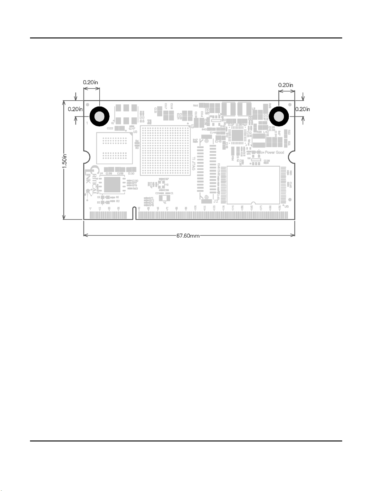
1.5 Module Dimensions
A dimensioned drawing of module is included below in Figure 1.
MityDSP-L138 Carrier Board Design Guide
March 5, 2014
Figure 1: MityDSP-L138, MitySOM-1808, MitySOM-1810 MityDSP-6748 Mechanical Drawing
Page 3 of 17
Critical Link reserves the right to make corrections, modifications, enhancements, and other changes to this document at any time and without notice.
Document Revision: 1.7 – MityDSP-L138 Revision 4A
MityDSP-L138 Carrier Board Design Guide
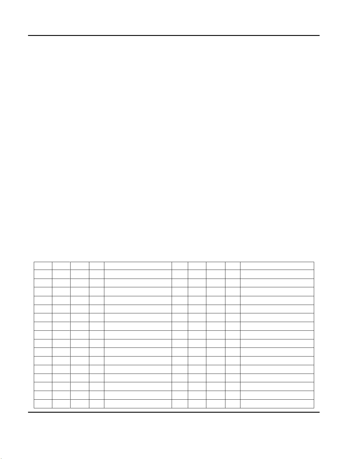
Pin
Ball
Type
I/O
Signal
Pin
Ball
Type
I/O
Signal
1 - PWR
-
+3.3 V in
2 - PWR
-
+3.3 V in
3 - PWR
-
+3.3 V in
4 - PWR
-
+3.3 V in
5 - PWR
-
+3.3 V in
6 - PWR
-
+3.3 V in
7 - PWR
-
GND
8 - PWR
-
GND
9 - PWR
-
GND
10 - PWR
-
GND
11
K14 D I
RESET_IN#
12 - D I EXT_BOOT#
13
J1 D O
SATA_TX_P
14
A4 M I/O
GP0_7
15
J2 D O
SATA_TX_N
16
A3 M I/O
GP0_10
17
L1 D I
SATA_RX_P
18
A2 M I/O
GP0_11
19
L2 D I
SATA_RX_N
20
A1 M I/O
GP0_15
21
P16 D I
USB0_ID
22
B4 M I/O
GP0_6
23
P18 D I/O
USB1_D_N
24
B1 M I/O
GP0_14
25
P19 D I/O
USB1_D_P
26
B2 M I/O
GP0_12
27
N19
D O USB0_VBUS
28
B3 M I/O
GP0_5
29
M18
D
I/O
USB0_D_N
30
C2 M I/O
GP0_13
31
M19
D
I/O
USB0_D_P
32
C3 M I/O
GP0_1
March 5, 2014
2 Connectors
All types of MityDSP utilize SO-DIMM style edge-connectors for main connectivity with the end user application
PCB. These connectors were chosen for their high density, compact size, ease of procurement, and low cost.
With edge connectors, a physical socket component is only required on one side – the main PCB side. The SODIMM standard also allows the MityDSP module to lay flat, in parallel with the main PCB, as they were intended
for use by memory modules in compact equipment, such as laptops.
2.1 Card-edge compatibility
The MityDSP-L138 family of SOMs is designed to plug into a 200-pin SO-DIMM DDR2 RAM socket. These sockets
are used for memory on PC laptop systems. Please note that the MityDSP is NOT electrically compatible with
the DDR2 socket standard, and intermixing modules/sockets from the two standards would very possibly cause
permanent damage to one or both sides.
2.2 Module Pin-out
The SO-DIMM card edge interface contains 4 classes of signals:
Power (PWR)
Dedicated signals mapped to the processor (D)
Dedicated signals when NAND memory is populated on the module (D*)
Multi-function signals mapped to the processor (M)
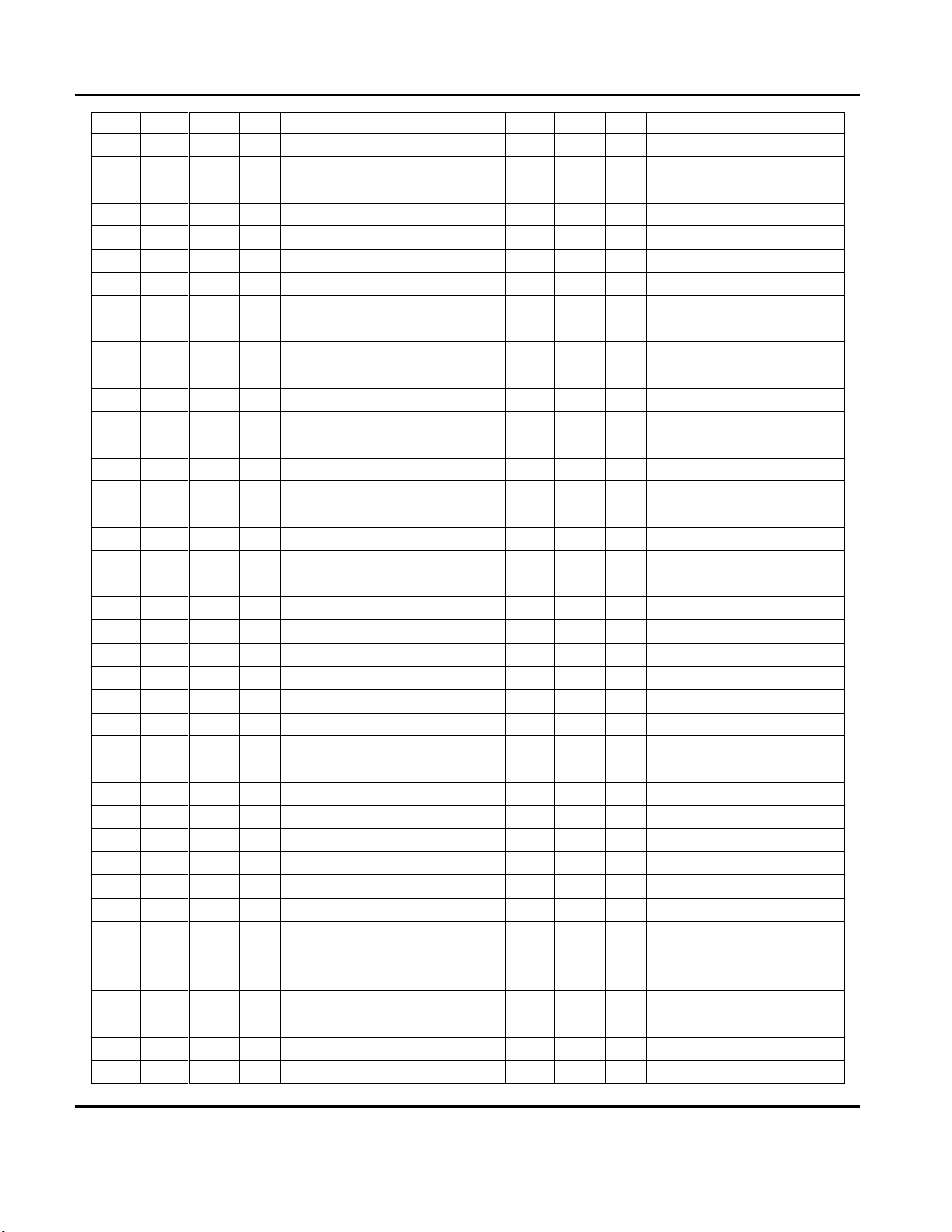
Table 1: MityDSP-L138, MitySOM-1808, MitySOM-1810 and MityDSP-6748 Card-edge (J100) Pin-out
Page 4 of 17
Document Revision: 1.7 – MityDSP-L138 Revision 4A
Critical Link reserves the right to make corrections, modifications, enhancements, and other changes to this document at any time and without notice.
MityDSP-L138 Carrier Board Design Guide
Pin
Ball
Type
I/O
Signal
Pin
Ball
Type
I/O
Signal
33
K18 D O
USB0_DRVVBUS
34
C4 M I/O
GP0_4
35 - D - 3V RTC Battery
36
C5 M I/O
GP0_3
37 - PWR
-
+3.3 V in
38 - PWR
-
+3.3 V in
39 - PWR
-
+3.3 V in
40 - PWR
-
+3.3 V in
41 - PWR
-
GND
42 - PWR
-
GND
43
H17
D
I/O
SPI1_MISO
44
D4 M I/O
GP0_2
45
G17
D
I/O
SPI1_MOSI
46
E4 M I/O
GP0_0
47
H16
D
I/O
SPI1_ENA
48
F4 M I/O
GP0_8
491 G19
D
I/O
SPI1_CLK
50
D5 M I/O
GP0_9
51
F18 M I/O
SPI1_SCS[1]
52
A12
M
I/O
MMCSD0_DAT[7]
53 - D - Reserved
54
C11 M I/O
MMCSD0_DAT[6]
552 G16
D
I/O
I2C0_SCL
56
E12 M I/O
MMCSD0_DAT[5]
572 G18
D
I/O
I2C0_SDA
58
B11 M I/O
MMCSD0_DAT[4]
59
F16 M I/O
UART2_TXD / I2C1_SDA
60
E11 M I/O
MMCSD0_DAT[3]
61
F17 M I/O
UART2_RXD / I2C1_SCL
62
C10 M I/O
MMCSD0_DAT[2]
63 - PWR
-
GND
64 - PWR
-
GND
65
F19 M O
UART1_TXD
66
A11
M
I/O
MMCSD0_DAT[1]
67
E18 M I
UART1_RXD
68
B10 M I/O
MMCSD0_DAT[0]
69
E16 M O
MDIO_CLK
70
A10
M
I/O
MMCSD0_CMD
71
D17
M
I/O
MDIO_D
72
E9 M O
MMCSD0_CLK
73
D19
M I MII_RXCLK
74
D3 M I
MII_TXCLK
75
C17 M I
MII_RXDV
76
E3 M O
MII_TXD[3]
77
D16
M I MII_RXD[0]
78
E2 M O
MII_TXD[2]
79
E17 M I
MII_RXD[1]
80
E1 M O
MII_TXD[1]
81
D18
M I MII_RXD[2]
82
F3 M O
MII_TXD[0]
83
C19 M I
MII_RXD[3]
84
C1 M O
MII_TXEN
85 - PWR
-
GND
86 - PWR
-
GND
87
C18 M I
MII_CRS
88
D1 M I
MII_COL
89
C16 M I
MII_RXER
90 - D - NC
91
A18
M O EMA_CS[0]
92
W15
M
I/O
UPP_CHA_START
93
B15
D* O EMA_OE
94
V15 M I
VP_CLKIN1
95
C15 M O
EMA_BA[0]
96
U18
M
I/O
UPP_D[15] / RMII_TXD[1]
97
A15
M O EMA_BA[1]
98
V16 M I/O
UPP_D[14] / RMII_TXD[0]
99
C14 M O
EMA_A[0]
100
R14 M I/O
UPP_D[13] / RMII_TXEN
101
D15
D* O EMA_A[1]
102
W16
M
I/O
UPP_D[12] / RMII_RXD[1]
103
B14
D* O EMA_A[2]
104
V17 M I/O
UPP_D[11] / RMII_RXD[0]
105
D14
M O EMA_A[3]
106
W17
M
I/O
UPP_D[10] / RMII_RXER
107 - PWR
-
GND
108 - PWR
-
GND
109
A14
M O EMA_A[4]
110
W18
M
I/O
UPP_D[9] / RMII_REF_CLK
111
C13 M O
EMA_A[5]
112
W19
M
I/O
UPP_D[8] / RMII_CRS_DV
113
E13 M O
EMA_A[6]
114
V18 M I/O
UPP_D[7]
March 5, 2014
Critical Link reserves the right to make corrections, modifications, enhancements, and other changes to this document at any time and without notice.
Page 5 of 17
Document Revision: 1.7 – MityDSP-L138 Revision 4A

MityDSP-L138 Carrier Board Design Guide
Pin
Ball
Type
I/O
Signal
Pin
Ball
Type
I/O
Signal
115
B13 M O
EMA_A[7]
116
V19 M I/O
UPP_D[6]
117
A13
M O EMA_A[8]
118
U16
M
I/O
UPP_CHA_ENABLE
119
D12
M O EMA_A[9]
120
U19
M
I/O
UPP_D[5]
121
C12 M O
EMA_A[10]
122
T16 M I/O
UPP_D[4]
123
B12 M O
EMA_A[11]
124
R18 M I/O
UPP_D[3]
125
D13
M O EMA_A[12]
126
R19 M I/O
UPP_D[2]
127
D11
M O EMA_A[13]
128
T15 M I/O
UPP_CHA_WAIT
129 - PWR
-
GND
130 - PWR
-
GND
131
E6
D*
I/O
EMA_D[15]
132
R15 M I/O
UPP_D[1]
133
C7
D*
I/O
EMA_D[14]
134
P17 M I/O
UPP_D[0]
135
B6
D*
I/O
EMA_D[13]
136
U17
M
I/O
UPP_CHA_CLK
137
A6
D*
I/O
EMA_D[12]
138
J4 M I/O
UPP_CHB_ENABLE
139
D6
D*
I/O
EMA_D[11]
140
K3 M O
VP_CLKOUT2
141
A7
D*
I/O
EMA_D[10]
142
H3 M I
VP_CLKIN2
143
D9
D*
I/O
EMA_D[9]
144
G3 M I/O
UPP_CHB_WAIT
145
E10
D*
I/O
EMA_D[8]
146
G2 M I/O
UPP_CHB_START
147
D7
D*
I/O
EMA_D[7]
148
G1 M I/O
UPP_CHB_CLK
149
C6
D*
I/O
EMA_D[6]
150
W14
M I VP_CLKIN0
151 - PWR
-
GND
152 - PWR
-
GND
153
E7
D*
I/O
EMA_D[5]
154
P4 M I/O
LCD_D[15]
155
B5
D*
I/O
EMA_D[4]
156
R3 M I/O
LCD_D[14]
157
E8
D*
I/O
EMA_D[3]
158
R2 M I/O
LCD_D[13]
159
B8
D*
I/O
EMA_D[2]
160
R1 M I/O
LCD_D[12]
161
A8
D*
I/O
EMA_D[1]
162
T3 M I/O
LCD_D[11]
163
C9
D*
I/O
EMA_D[0]
164
T2 M I/O
LCD_D[10]
165
C8 M O
EMA_WEN_DQM[0]
166
T1 M I/O
LCD_D[9]
167
A5 M O
EMA_WEN_DQM[1]
168
U3 M I/O
LCD_D[8]
169
D8 M O
EMA_SDCKE
170
U2 M I/O
LCD_D[7]
1713 B7 M O
EMA_CLK
172
U1 M I/O
LCD_D[6]
173 - PWR
-
GND
174 - PWR
-
GND
175
B9
D* O EMA_WE
176
G4 M O
LCD_VSYNC
177
A9 M O
EMA_CAS
178
H4 M O
LCD_HSYNC
179
A16
M O EMA_RAS
180
V3 M I/O
LCD_D[5]
181
B17 M O
EMA_CS[2]
182
F1 M O
LCD_PCLK
183
F9 M O
EMA_CS[4]
184
V2 M I/O
LCD_D[4]
185
B16 M O
EMA_CS[5]
186
V1 M I/O
LCD_D[3]
187
T17 D O
RESET_OUT
188
W3 M I/O
LCD_D[2]
189
J3 M I
VP_CLKIN3
190
W2 M I/O
LCD_D[1]
191
K4 M O
VP_CLKOUT3
192
W1 M I/O
LCD_D[0]
193
F2 M O
LCD_MCLK
194
R5 M O
LCD_AC_ENB_CS
195 - PWR
-
GND
196 - PWR
-
GND
March 5, 2014
Critical Link reserves the right to make corrections, modifications, enhancements, and other changes to this document at any time and without notice.
Page 6 of 17
Document Revision: 1.7 – MityDSP-L138 Revision 4A
 Loading...