

Page 1
NACHBAU Assembly Instructions
Author: Christian Aschof, cascho@mac.com
Version 0.4 from August 10, 2012
Translator: Hesky Fisher, hesky@wyolum.com
These instructions are for:
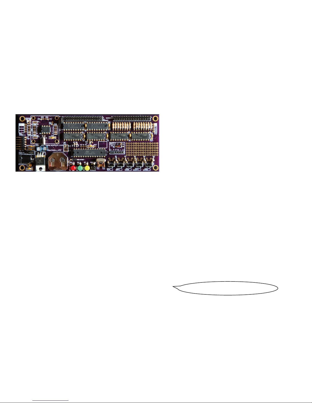
The NachBau_V02-Board was built
from:
to:
To-Do:
CC BY-NC-SA 3.0:
Attribution - Non
Commercial - Share Alike 3.0
You are free:
to copy, distribute and transmit the work
to adapt the work
With the following requirements:
Attribution - You must attribute the work in the
manner specied by the author or licensor (but
not in any way that suggests that they endorse
you or your use of the work).
Noncommercial - You may not use this work for
commercial purposes.
Share Alike - If you alter, transform, or build
upon this work, you may distribute the resulting
work only under the same or similar license to
this one.
Page 2
Forward
These instructions are for the assembly of a NachBau_V02-board.
The NachBau_V02 (NachBau is German for „replica“) is an LED matrix
display driver. This means that one can use it to control a 16x16 LED
matrix display (i.e. 256 LEDs). The LEDs are driven via multiplexing.
The NachBau_V02 board also has clock support. It has a battery-backed
real time clock and can update the time, based on the DCF77 time
signal from the German National Physics Lab in Braunschweig.
Finally, the board can be chained: one can connect multiple boards
and control several 16x16 LED matrices to make larger displays.
The board is therefore especially suitable for:
• Clock projects, such as word clocks, clocks with scrolling text, binary clocks, etc.
• Large-format versions of games, such as Pong, Maze or other low resolution games (see also the Mignon Game Kit from Olaf Val).
• Display projects, such as tickers, temperature displays, advertising, etc., especially when the displayed text is time dependent (e.g., automatic
displays of „We're open“ / „We're closed“ driven by opening hours, etc.)
The idea for this board came from the QLOCKTWO replica project. There are instructions at http://code.google.com/p/grosses-bastelwochenende on
how to assemble a word clock from many parts. To somewhat tame the chaos and failure rate, Justin and Anool from WyoLum redesigned and streamlined the boards. The three boards from that project (control board, anode multiplexer, cathode multiplexer) plus the Really Bare Bones Board from
Jee-Labs/Modern Devices are now combined in this one board.
The boards and the associated circuits are released as Open Hardware. The plans and Gerber les can be found at http://code.google.com/p/clockthree/.
The ATMEGA328 chip from the kit is compatible with Arduino and can be reprogrammed for use in your own projects using an FTDI cable and the
Arduino IDE. Sample code can be found at http://code.google.com/p/grosses-bastelwochenende/.
Cool, no? So then: Warm up your soldering iron and let's go. Or as Yoda already said in the QLOCKTWO Replica project:
May the force be with you.
i
Page 3
Safety Notices
Soldering irons, hot glue guns, hot glue and hot-air
guns are hot, as the names imply. Cleaning agents,
especially rubbing alcohol, are ammable.
During assembly you will be exposed to voltages
and current. If the NachBau_V02-Board is powered
by a battery or DC adapter (the recommended
way), then this won’t be a problem. However, using
a built-in AC power supply exposes you to mortal
danger.
The assembly of the NachBau_V02-Board is dangerous. Carpet knives, scalpels, glass edges and drill
bits are sharp. SMD tweezers and drill bits are
pointy. Snipping o the legs of components send
sharp pieces of wire ying around. These can harm
your eyes.
If you use „super bright“ LEDs then you must never
look directly at the LEDs, especially while uploading
the rmware, since random lights may turn on due
to junk data in the shift registers.
An LED matrix driven by multiplexing operates at
high frequency and causes electromagnetic interference in the form of radio waves. This currently
interferes with the DCF77 receiver, which we plan
to x. For other things that might be disturbed by
such interference (e.g. pacemakers) you must take
your own precautions.
Solder fumes, cleaning agents, sanding dust, glue,
paint, etc., are almost always toxic.
In conclusion: The assembly of a NachBau_V02-Board
is in every way dangerous. It is advisable to wear eye
protection, gloves and to have a rst-aid kit ready.
So, man or mouse? Right. The life of a tinkerer is
dangerous in and of itself. So, use your head, work
carefully, and press on.
Page 4

Version history
Links
V 0.1 24.4.2012 Created.
V 0.2 2.7.2012 Resistance values adjusted (the colors were wrong).
V 0.3 11.7.2012 Page 8: Adjusted resistor values; Page 15: Claried empty resistor slots.
V 0.4 10.8.2012 Removed color values of resistors.
Current rmware and related les: http://code.google.com/p/grosses-bastelwochenende/
Wyolum (distributor of the board and kit): http://wyolum.com
Schematics and Gerber les: http://code.google.com/p/clockthree/
Author‘s blog: http://christians-bastel-leben.blogspot.com/
Arduino: http://www.arduino.cc/
Jee-Labs (RBBB/USB-BUB): http://jeelabs.org/
Reichelt: http://www.reichelt.de/
Pollin: http://www.pollin.de/
Page 5
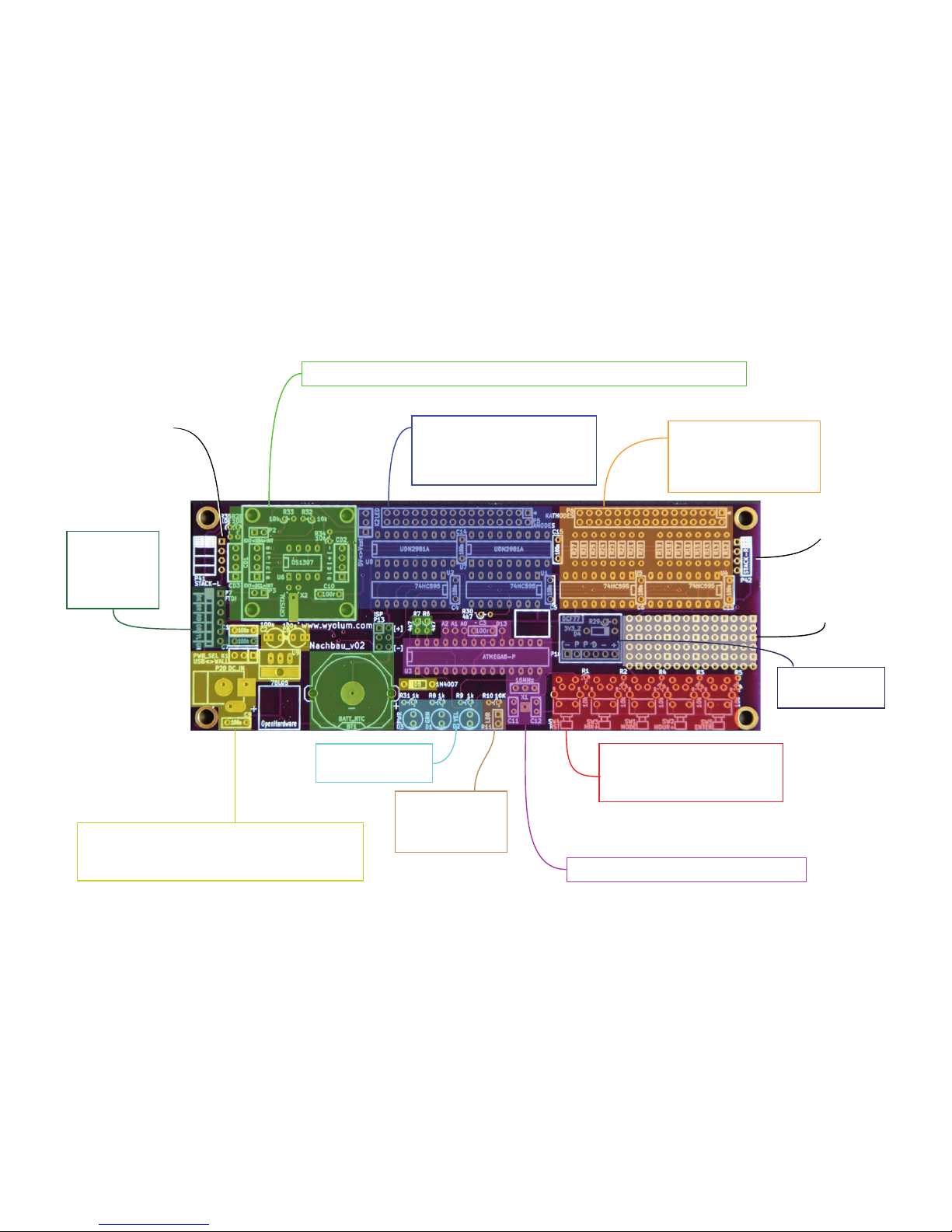
Layout of the board
Real time clock (DS1307, crystal, cattery holder for CR2032, pull up resistors)
ATMEGA328-MCU with crystal/resonator
Power supply (voltage regulator, power jack,
capacitors, blocking diode)
Status LEDs with
resistors
5 buttons (Mode, H+, M+,
Enter, and Reset) with pull
down resistors
Anode multiplexers (shift
registers, Darlington arrays,
ltering capacitors, terminal
block)
Cathode multiplexers
(shift registers, current
limiting resistors,
terminal block)
FTDI and ISP
Headers for
rmware
updates
3.3 Volts
for DCF77
Prototyping
Area
Photoresistor
and resistor as
voltage divider
Stack-L
(for larger
matrices)
Stack-R
(for larger
matrices)
Page 6

A few words in advance...
Components are usually soldered onto a circuit board in height order, shortest rst. This allows you to ip the board and have the component rest on
the table with the board on top of it. Otherwise, when you ip the board for soldering, the board will rest on the taller components and the shorter
ones will just fall out.
The downside of this method is that you have to assemble the entire board before testing. If you made a mistake, it can then be hard to nd.
In this tutorial, we are attaching components grouped by functionality instead. We will then test each section separately. When attaching components with long legs, just bend them so they stay attached when you ip the board. You can use masking tape to keep other components in place
while soldering.
Many features of the board are optional. To use it as a 16x16 LED matrix driver only the ATMEGA328-MCU along with the anode and cathode multiplexers are required. The rest is optional:
• To use it as a clock you will need the DS1307 real time clock. With the battery backing, it will continue to keep time when disconnected from a
power supply.
• For automatic time updates you can add the DCF77 receiver. The time will update any time it receives a valid signal. The receiver can be left on
permanently (by using the jumper on the receiver terminal strip to connect P to -) or you can connect P to D and, which connects pin D13 on the
ATMEGA328-MCU to PON, and you can set the pin high to turn the receiver o when you like.
• If you have a stable 5-6 volt supply, (e.g., a USB power supply or batteries), then you can connect those directly to the voltage regulator. If you
want to use an external power supply, then you need to set up the voltage regulation section and then the board will be able to take 7-12 volt. By
the way, you can use the jumper next to the anode multiplexers („5V<->Vext”) to send the external voltage to the Darlington arrays to increase
the brightness of the LEDs. But this is for experts and is only briey covered in this tutorial.
• You can add a photoresister to control the brightness of the display based on the ambient light level.
• You can add the FTDI port and ISP header to program the microcontroller.
• Finally: Instead of the DS1307 you can also use a Chrono-Dot or a DS3231N. Stack-L and Stack-R can be used to chain boards to power a larger
display. Neither is supported with the current word clock rmware but it wouldn‘t be that hard to add.
Page 7

Step 1: The ATMEGA328-MCU
Required parts: Placing the parts:
1*ATMEGA328
1*crystal 16 MHz
2*C 22 pF
1*resonator 16 MHz
or
1*crystal und 2*C 22 pF
or
1*resonator
1*ATMEGA328
(make sure to align the notch!)
The 16 MHz resonator is
soldered into these
holes.
The 16 MHz Crystal is
soldered into these two
holes. Then you also
need 2*22 pF capacitors
(C11 and C12).
Right at the start you have a tough choice to make. Do you use a 16 MHz resonator or a 16 MHz crystal with
two 22 pF capacitors as the clock for the ATMEGA328-MCU? One tip: They‘re the same. A resonator consists of a
crystal with two capacitors. You should choose whichever one is easier to nd.
Make sure to line up the small semicircular notch in the short side of the ATMEGA328 with the mark on the
board.
Experienced solderers can attach the MCU directly onto the board. Beginners should use the socket (Make sure
to line up the notch in the socket as well) and later add the MCU. This is because the MCU is more sensitive to
the heat from the soldering iron. This will not aect the overall height of the board because there are still taller
components that aect the overall clearance.
We don‘t need the small solder pad labeled „X1“ so we will ignore it. It is there because some crystals need a
ground plane.
Page 8

Testing the ATMEGA328-MCU (preparing the power supply)
In order to test the MCU we rst need power. We have two options: the FTDI connector or an external power supply. Let’s rst try the FTDI option
since we’ll need some of the same parts for the external power supply.
First, we’ll solder on a jumper that we can use to choose between USB and external power.
Required parts: Placing the parts:
1*Pinheader
(3 Pins)
1*Jumper
We use this jumper to choose the power
source: either the FTDI connector (Position:
USB) or an external supply (Position: WALL).
Then we‘ll attach the power LED so we can
tell when the power is on.
1*red LED
1*1 kOhm
Attention! The LED has a long
and a short leg. The long leg
should go through the red
hole in the diagram and the
short one through the blue hole.
Page 9

Testing the ATMEGA328-MCU (power via FTDI)
Required parts: Placing the parts:
1*Pinheader
(6 Pins)
1*100 nF
1*10 kOhm
For the FTDI connector you can use either a straight or right-angled header, whichever you prefer. The pin header and capacitor are only
needed when using an FTDI cable or ISP header to program the ATMEGA328-MCU.
The resistor by the reset switch must be added even if you don’t intend to add a button. If it is not, then the Reset pin of the
ATMEGA328-MCU will hang and the microcontroller will constantly reset itself.
If you have an FTDI cable or a USB cable and a USB-BUB (e.g., from Jee-Labs), then you can now test the ATMEGA328-MCU.
Open the Serial-Monitor in the Arduino-IDE with the right settings (Serial-Port: something with „USB“ (The name is dierent on every system),
Board: Arduino Duemilanova; Serial speed in the monitor: 57600) then the MCU will output:
Qlockthree is initialazing...
... done and ready to rock!
The red power inicating LED will only light up using an external power supply.
Page 10

Testing the ATMEGA328-MCU (external power supply)
Required parts: Placing the parts:
1*power Jack
1*voltage regulator
1*blocking diode
2*100 nF
2*100 µF
Solder the green and yellow LEDs plus their 1
kOhm resistors just like you did the power
LED. Here too, place the longer leg of the LED
in the hole marked red in the diagram. These
LEDs and resistors must be soldered on
regardless of which power source you use.
Make sure to align the voltage regulator so that its metal plate will lie on the rectangular solder
plate. Face the side with writing toward the real time clock area and face the metal part toward
the open source hardware logo.
The large capacitors (100 µF) have polarity. The leg with the minus sign goes in the hole with the
mark (The two capacitors‘ negative poles face each other). There are two holes for the other leg
to handle capacitors with dierent leg spacing.
For testing purposes, when you use external power (jumper to the WALL position) then the
yellow and green LEDs will quickly blink three times.
Page 11

Step 2: The DS1307 real time clock
Required parts: Placing the parts:
As with the reset button you
must add on pull down resistors
(10 kOhm) to the H+, M+ and
Mode switches. If you forget
then those pins will hang and
the actions will constantly be
triggered. The DS1307 won‘t
work correctly since the time is
constantly being set.
2*4,7 kOhm
1*100 nF
1*clock crystal
1*DS1307
1*battery holder
and CR2032 battery
Make sure that the notch on the DS1307 lines up with the mark on the board.
Before soldering the battery holder, tin the round pad with the minus sign to make sure the battery makes a
good contact with the board.
The time crystal is soldered so that, when bent over, the housing will lie on the long rectangular solder pad. In
contrast to the crystal next to the ATMEGA328-MCU, here we do need the ground plane (Those interested in
the details should google “dallas real time clock crystal considerations.) It is essential to solder the housing of
the crystal to the ground plane. Using additinal soldering ux helps here...
For testing purposes, if the clock is properly attached then the green LED will start blinking once per second
(after the initial three fast ashes).
Page 12

Step 3: Prepare the DCF77 receiver
Required parts: Placing the parts:
1*220 Ohm
1*3.3 volt zener diode
pin header and jumper (optional)
The zener diode and the 220 Ohm resistor make a voltage divider to produce the 3.3 volt that the
DCF77 receiver requires.
The pin header and jumper are optional. They switch what is connected to the PON pin on the
receiver (that can be used to put the receiver to sleep). If you attach it to ground, then the receiver
will stay on permanently. Alternatively, you can connect it to pin D13 of the ATMEGA328-MCU, so
you can put the receiver to sleep whenever you want.
The pin assignments on the board correspond to the receiver by Pollin. Other receivers might
require extra circuitry which can be placed in the prototyping area of the board.
If the receiver has a good signal then the yellow LED will blink once per second (but a shorter blink
than the green LED). A DCF77 receiver can take up to a half an hour before it is ready!
3.3 volts from
the voltage divider
Ground
Ground
Data
PON
PON
These two
pins are
connected.
Page 13

Step 4: The anode multiplexer
Required parts: Placing the parts:
This resistor (4.7 kOhm)
must be soldered on
before the rst test of
the matrix. It sets the
output of the shift
registers before they
are initialized. Otherwise, the LEDs will light
uncontrolled and can
burn out.
2*UDN2981A
Darlington arrays
2*74HC595
shift registers
4*100 nF
1*pin header
and Jumper
Just like all the other chips, make sure to line up the notch on the chip with the mark on the board. The 74HC595
shift registers and the UDN2981A Darlington arrays face opposite directions.
You can use the jumper to change the voltage input of the Darlington arrays. If it is set to „5V“, then they will get the
same 5V as the rest of the board. If it is set to „Vext“ then it will receive its input directly from the external power
supply.
You can use this to change the brightness of the LEDs. However, if you use this then you must gure out, on your
own, what value to use for the resisters on the cathode multiplexer (R12-R27). You would need to use an oscilloscope to measure the voltage on the output of the Darlington arrays and calculate the appropriate resistor value
using one of the many online resistor calculators. As you can see, this is an advanced option intended for experts.
Page 14

Step 5: The cathode multiplexer
Required parts: Placing the parts:
2*74HC595
shift registers
2*100 nF
16*6,8 Ohm
or short links
Make sure to line up the notch on the 74HC595 shift registers with the mark on the board.
Here you have another tough decision. Many hobbyists drive their matrix without resistors. At rst this seems odd. We all know that LEDs need resistors.
However, the Darlington arrays have resistors so these may be enough and there have yet to be reports of LEDs burning out. Especially, since the silver
wires that connect the LEDs in the matrix are good heat conductors and good heat removal is essential to the long life of LEDs. So thrill seekers can
replace the resistors with wires or jumpers. Those who want to be sure can add the resistors from the kit. These are small, only 6.8 ohm.
Those who set the jumper to „Vext“ must adjust the values of these resistors as previously discussed.
Page 15

Final touches
If you add right angled buttons then you can still use these
holes to attach additional buttons that can be
exposed outside of your project’s housing.
The enter button
can be picked up here
and attached to one of the
analog pins on the MCU.
solder on
1*100 nF
The rst column of the prototyping
area is attached to Vcc and the second
to ground. The other holes are
connected to each other in rows of
three.
You can burn a bootloader
onto the ATMEGA328-MCU
using the ISP header .
Connection for the photoresistor
and resistor as voltage divider.
These resistor slots
remain empty.
This resistor is no
longer needed.
Page 16

Connection to the matrix
123456789101112131415
16
1615141312111098765432
1
Anode pins (rows) are numbered from left to right:
Cathodes pins (columns) are numbered from right to left:
Top left.
Top left.
Top right.
Top right.
Bottom right.
Bottom right.
Bottom left.
Bottom left.
CONGRATULATIONS!
The pairs of pins are
all connected in
tupels (e.g. for
corner LEDs)
 Loading...