

Page 1
5900333
RR
TM
Optipay BV
DBV-301 Bill Validator
Operation and Maintenance Manual
(Revision 1)
Includes configuration setup using a Palm Pilot
Setting Module
May 05
1-800-628-8363
RR
JCM Part Number 980-000103.Rev. 1
5900333
Page 2

JCM is a registered trademark of JCM American Corporation. All other product names mentioned herein may be
registered trademarks or trademarks of their respective companies. Furthermore,
in each case throughout this publication.
™
, ® and © are not always mentioned
Page 3

Optipay™ BV
Table of Contents
TOC
Page
1 GENERAL INFORMATION...................................................................................1-1
Model and Type Classification ................................................................................... 1-1
Precautions .................................................................................................................. 1-2
User cautions ............................................................................................................................1-2
Component Names...................................................................................................... 1-3
General Specifications................................................................................................ 1-4
Retrieving Bills ............................................................................................................ 1-5
Cabling .........................................................................................................................1-6
Dimensions .................................................................................................................. 1-7
Cash Box Label............................................................................................................ 1-8
DIP Switch Label.......................................................................................................... 1-8
Country Codes............................................................................................................. 1-9
2 INSTALLATION / OPERATION ............................................................................2-1
Installation....................................................................................................................2-1
Mounting the unit ....................................................................................................................... 2-1
Removing the bill guide .............................................................................................................2-1
Input/Output Circuitry ................................................................................................. 2-2
Connector Pin Assignment ........................................................................................ 2-2
DIP Switch Settings..................................................................................................... 2-3
Operational Flowchart................................................................................................. 2-4
Clearing a Bill Jam ...................................................................................................... 2-5
When a bill is jammed in the Stacker section: ........................................................................... 2-5
When a bill is jammed in the Validator section: ......................................................................... 2-5
Preventive Maintenance.............................................................................................. 2-5
Cash box Preventive Maintenance (P/M).................................................................................. 2-6
3 MDB PROTOCOL .................................................................................................3-1
4 DISASSEMBLY.....................................................................................................4-1
Circuit Board Disassembly......................................................................................... 4-1
Removing the CPU and Power Supply boards ......................................................................... 4-1
Pusher Mechanism Disassembly............................................................................... 4-3
Timing Belt removals .................................................................................................................4-3
Removing the drive and stack motor ......................................................................................... 4-3
Upper Guide Disassembly .......................................................................................... 4-5
Sensor board removal ...............................................................................................................4-5
O-ring removal...........................................................................................................................4-6
Lower Guide Disassembly.......................................................................................... 4-6
MAG board removal ..................................................................................................................4-6
5 WIRING DIAGRAMS.............................................................................................5-1
DBV-301 Interconnect ................................................................................................. 5-1
DBV-301 Interconnect Continued.............................................................................................. 5-2
6 TROUBLE SHOOTING .........................................................................................6-1
Introduction.................................................................................................................. 6-1
Failure Classifications ................................................................................................ 6-1
Test Mode Entry Failure Flowchart ............................................................................ 6-1
5900333 © 2005 JCM-American Corporation
i
Page 4

Optipay™ BV
Table of Contents
Continued
Test mode entry failure flowchart (continued)............................................................................6-2
Incorrect initial operation flowchart............................................................................................ 6-3
Rejected or poorly accepts bills flowchart .................................................................................6-4
Improper bill transfer flowchart ..................................................................................................6-5
Page
7 FLASH MEMORY DOWNLOAD ...........................................................................7-1
Tool Requirements ...................................................................................................... 7-1
Requirements ............................................................................................................................7-1
Information Menu Selection ....................................................................................... 7-1
Diagnostics Menu Selection....................................................................................... 7-3
Program Download Menu Selection .......................................................................... 7-3
Selecting a Download ROM ........................................................................................ 7-3
Accepting Log Menu Selection .................................................................................. 7-4
DIP Switch Settings..................................................................................................... 7-6
Test mode set-up ....................................................................................................................... 7-6
Setting the test mode switches..................................................................................................7-6
Test Mode Details ........................................................................................................ 7-8
Acceptor Sensor Test Details ....................................................................................................7-8
Stacker SensorTest Details .......................................................................................................7-8
DIP Switch Logic Test................................................................................................................7-9
Error Codes.................................................................................................................. 7-9
Error Code Table ....................................................................................................................... 7-9
Reject Code Table ................................................................................................................... 7-10
Sensors, Circuit Boards, Motors and Cash Box Locations....................................7-11
8 EXPLODED VIEWS/PARTS LISTS ......................................................................8-1
DBV Primary Component Parts.................................................................................. 8-1
DBV Primary Parts List ............................................................................................... 8-2
Frame and Upper/Lower Guide Exploded View........................................................ 8-2
Frame and Upper/Lower Guide Parts List................................................................. 8-3
Pusher Mechanism Assembly Exploded View ......................................................... 8-5
Pusher Mechanism Assembly Exploded View Parts List ........................................ 8-6
Cash Box Unit Exploded View.................................................................................... 8-7
Cash Box Unit Parts List............................................................................................. 8-8
9 INDEX....................................................................................................................9-1
5900333 © 2005 JCM-American Corporation
ii
Page 5

Optipay™ BV
List of Figures
LOF
Figure 1-1 Optipay™ BV DBV-301 Bill Validator ................................................... 1-1
Figure 1-2 Precautionary Symbols......................................................................... 1-2
Figure 1-3 Bill Validator Top and Rear View.......................................................... 1-3
Figure 1-4 Bill Validator Bottom and Right Side View............................................ 1-3
Figure 1-5 Initial Bill Retrieval Steps ...................................................................... 1-5
Figure 1-6 Final Bill Retrieval Steps....................................................................... 1-5
Figure 1-7 Cable Connector Locations .................................................................. 1-6
Figure 1-8 Bill Validator Dimensions...................................................................... 1-7
Figure 1-9 Cash Box Front Label........................................................................... 1-8
Figure 1-10 DIP Switch Side Label .......................................................................... 1-8
Figure 2-1 Bill Validator Mounting Locations ......................................................... 2-1
Figure 2-2 Bill Validator Removal .......................................................................... 2-1
Figure 2-3 Bill Guide Removal ............................................................................... 2-1
Figure 2-4 Bill Validator-to-Controller I/O Circuit and Pin-out Identification
Schematic............................................................................................. 2-2
Figure 2-5 Bill Validator’s Plug Interconnect Pin Assignment Diagram ................. 2-2
Figure 2-6 Typical Interconnect Plug Pin Assignment Diagram............................. 2-3
Figure 2-7 DIP Switch Location ............................................................................. 2-3
Figure 2-8 Bill Validator Operational Flowchart ..................................................... 2-4
Figure 2-9 Clearing a Jammed Stacker Bill ........................................................... 2-5
Figure 2-10 Clearing a Jammed Validator ............................................................... 2-5
Figure 2-11 Upper Guide and Stacker Sensors and Rollers.................................... 2-5
Figure 2-12 Lower Guide Sensors and Rollers........................................................ 2-5
Figure 2-13 Cash Box Sensors................................................................................ 2-6
Figure 4-1 Bill Validator Mounting Locations ......................................................... 4-1
Figure 4-2 Lower Guide Removal .......................................................................... 4-1
Figure 4-3 Validator Cover Removal...................................................................... 4-1
Figure 4-4 Validator Face Plate Removal .............................................................. 4-1
Figure 4-5 Face Plate Rear Mounting View ........................................................... 4-2
Figure 4-6 Screw and Connector Removal and Circuit Board Access .................. 4-2
Figure 4-7 CPU Board Connector Removals......................................................... 4-2
Figure 4-8 CPU and Power Supply Board Connector Separation ......................... 4-2
Figure 4-9 Side Guide Removal............................................................................. 4-3
Figure 4-10 Front Guide Removal ........................................................................... 4-3
Figure 4-11 Pusher Mechanism Removal................................................................ 4-3
Figure 4-12 Timing Belt Removal ............................................................................ 4-3
Figure 4-13 Pusher Shaft C-Clip Ring Removal ...................................................... 4-4
Figure 4-14 Pusher Plate Removal.......................................................................... 4-4
Page
5900333 © 2005 JCM-American Corporation
iii
Page 6

Optipay™ BV
List of Figures
Continued
Figure 4-15 Shaft and Sleeve Removal ................................................................... 4-4
Figure 4-16 Retaining Screw Removals .................................................................. 4-4
Figure 4-17 Motor Guide Removal........................................................................... 4-4
Figure 4-18 Drive and Stack Motor Removal........................................................... 4-5
Figure 4-19 Upper Guide Removal .......................................................................... 4-5
Figure 4-20 Upper Guide Gear Removals ............................................................... 4-5
Figure 4-21 Sensor Board Removal ........................................................................ 4-5
Figure 4-22 Flexible Ribbon Cable Removal ........................................................... 4-5
Figure 4-23 Short Shaft and Gear Removal ............................................................ 4-6
Figure 4-24 Lower Long Shaft and Gear Removal .................................................. 4-6
Figure 4-25 Upper Long Shaft and Gear Removal .................................................. 4-6
Figure 4-26 O-Ring Removals ................................................................................. 4-6
Figure 4-27 Lower Bill Guide Removal .................................................................... 4-6
Figure 4-28 MAG Board Removal............................................................................ 4-7
Figure 4-29 Disconnect MAG Board Connector ...................................................... 4-7
Figure 5-1 DBV-301 Bill Validator Interconnect Wiring Diagram (Part 1) .............. 5-1
Figure 5-2 DBV-301 Bill Validator Interconnect Wiring Diagram (Part 2) .............. 5-2
Figure 6-1 DBV-301 Bill Validator Test Mode Failure Flow Chart
Diagram (Part 1) ................................................................................... 6-1
Figure 6-2 DBV-301 Bill Validator Test Mode Failure Flow Chart
Diagram (Part 2) ................................................................................... 6-2
Figure 6-3 DBV-301 Bill Validator Incorrect Initial Operation Flow Chart
Diagram ................................................................................................ 6-3
Figure 6-4 DBV-301 Bill Validator Rejects or Poorly Accepts Bills Flow Chart
Diagram ................................................................................................ 6-4
Figure 6-5 DBV-301 Bill Validator Improper bill transfer Flow Chart Diagram ....... 6-5
Figure 7-1 Typical M100/500 Series Palm Pilot® Handheld & Software ............... 7-1
Figure 7-2 PSP-03 Application Selection............................................................... 7-1
Figure 7-3 Settings Menu Selection....................................................................... 7-2
Figure 7-4 Information Menu Selection.................................................................. 7-2
Figure 7-5 Typical Configuration Settings.............................................................. 7-2
Figure 7-6 Acceptor Mode Selection...................................................................... 7-2
Figure 7-7 Acceptor Screen Functions .................................................................. 7-2
Figure 7-8 Returning to the Settings Screen.......................................................... 7-2
Figure 7-9 Diagnostics Mode Selection ................................................................. 7-3
Figure 7-10 Diagnostics Screen Functions .............................................................. 7-3
Figure 7-11 Program Download Menu Selection ..................................................... 7-3
Figure 7-12 Program Download Screen .................................................................. 7-3
Figure 7-13 ROM Select Screen.............................................................................. 7-4
Page
5900333 © 2005 JCM-American Corporation
iv
Page 7

Optipay™ BV
List of Figures
Continued
Figure 7-14 Download Transfer Screen................................................................... 7-4
Figure 7-15 Download Send Command................................................................... 7-4
Figure 7-16 Accepting Log Mode Selection ............................................................. 7-4
Figure 7-17 Accepting Log Menu............................................................................. 7-5
Figure 7-18 Viewing Record Log Data..................................................................... 7-5
Figure 7-19 Viewing Specific Log Data 1................................................................. 7-5
Figure 7-20 Viewing Page Two Log Data ................................................................ 7-5
Figure 7-21 Viewing Page Three Log Data.............................................................. 7-5
Figure 7-22 Viewing Page Four Log Data................................................................ 7-6
Figure 7-23 Sensors, Circuit Boards, and Motor Locations Diagram..................... 7-11
Figure 8-1 DBV Dual Bill Validator Primary Component Parts Exploded View
Diagram ................................................................................................ 8-1
Figure 8-2 Frame and Upper/Lower Guide Exploded View Diagram..................... 8-2
Figure 8-3 Pusher Mechanism Assembly Exploded View Diagram....................... 8-5
Figure 8-4 Cash Box Unit Exploded View.............................................................. 8-7
Page
5900333 © 2005 JCM-American Corporation
v
Page 8

Optipay™ BV List of Figures
THIS PAGE INTENTIONALLY LEFT BLANK
5900333 © 2005 JCM-American Corporation
vi
Page 9

Optipay™ BV
List of Tables
LOT
Table 1-1 Model Number Specifications ................................................................1-2
Table 1-2 Type Number Specifications..................................................................1-2
Table 1-3 DBV-301 Bill Validator Specifications....................................................1-4
Table 1-4 Cash Box Label Features ......................................................................1-8
Table 1-5 DIP Switch Label Features ....................................................................1-8
Table 1-6 Country Codes.......................................................................................1-9
Table 2-1 Connector Pin Designations ..................................................................2-2
Table 7-1 DIP Switch 1 Test Mode Settings ..........................................................7-6
Table 7-2 Acceptor Sensor Test Detail Listing ......................................................7-8
Table 7-3 Stacker Sensor Test Detail Listing ........................................................7-8
Table 7-4 Resulting DIP Switch Setting LED Flash Details ...................................7-9
Table 7-5 Error Code Blink Listing .........................................................................7-9
Table 7-6 Reject Code Listing .............................................................................7-10
Table 8-1 DBV Primary Parts List ..........................................................................8-2
Table 8-2 Frame and Upper/Lower Guide Parts List .............................................8-3
Table 8-3 Frame and Upper/Lower Guide Parts List .............................................8-6
Table 8-4 Cash Box Unit Parts List........................................................................8-8
Page
5900333 © 2005 JCM-American Corporation
vii
Page 10

Optipay™ BV List of Tables
THIS PAGE INTENTIONALLY LEFT BLANK
5900333 © 2005 JCM-American Corporation
viii
Page 11
Optipay™ BV
DBV-301 Bill Validator
Section 1
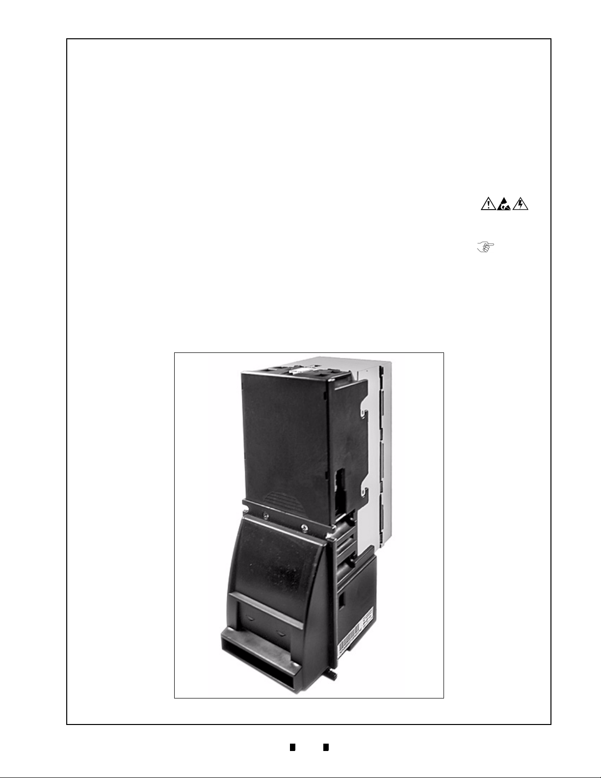
1 GENERAL INFORMATION
This section provides a general overview of the
advantages and options of the Optipay
DBV-301 Bill Validator pictured in Figure 1-1 .
This first section is designed to help you navigate
through this manual with ease and contains the following information:
•
Model and Type Classifications
•
Precautions
•
Component Names
•
General Specifications
•
Retrieving Bills
•
Cabling
•
Dimensions
•
Country Codes
™
BV
In order to make operation of this device and make
navigation within this manual easier, the following
illustrations were used within the text:
•
Safety instructions, which need to be
observed in order to protect the operators and
equipment, have been written in bold text and
have been given the pictographs:
•
Special Notes, which effect the use of the Bill
Validator, have been written in italic text and
have been given the pictograph:
•
Steps, requiring the operator to perform
specific actions are given sequential numbers
(1., 2., 3. etc.).
Model and Type Classification
Tables 1-1 and 1-2 provide definitions for the
model and type number codes found on the unit.
Figure 1-1 Optipay™ BV DBV-301 Bill Validator
5900333 © 2005 JCM-American Corporation
1-1
Page 12
Section 1 Optipay™ BV General Information
Table 1-1: Model Number Specifications
o
N
(1) Model Name
(2) Series Name
(3) CPU Board Type 0 : JCM Standard
(4) Power supply
(5) Stacker Type SU : Upward vertical
o
N
(1) Country Code
(2) Cash Box Capacity
(3) Faceplate Type
(4) Guide Width
(5) Cash Box Type
(6) Recycle Type (Optional)
(7) Interface Type
Model : DBV - 3 0 1 - SU
o
N
(1) (2)(3)(4) (5)
1 : 24 V DC
stacking
Table 1-2: Type Number Specifications
Type : * * * - * * * * * - D3
o
(1) (2)(3)(4)(5)(6) (7)
N
3 : 300 notes capacity
1 : JCM Standard
1 : 66 mm width
2 : 67 mm width
3 : 70 mm width
4 : 72 mm width
1 : Upward bill ejection box
0 : without recycle unit
1 : with recycle unit
D3 : ID-0D3 (MDB interface)
Precautions
1. (
Type 1
) Do not insert a torn, folded, or wet
bill, as this action may cause a bill jam inside
the unit.
2. (
Type 2
) Do not expose the unit to water.
The unit contains several precision electronic devices which can be damaged if
water or any liquid is sprayed or spilled into
the unit.
3. (
Type 3
) Do not install the unit into a dusty
environment. Dust may affect the sensor’s
performance.
User cautions
1. Be sure to turn the power off before plugging
or unplugging connectors.
2. Firmly close the unit’s transport path when
applying power.
3. When closing the units, ensure they click
into place. Make sure to open and close the
units gently, and take care that no dust or
other foreign objects enter when opening the
guides.
4. Do not allow inventory stock to endure high
temperature, high humidity or a dusty
environment.
5. Do not throw the unit or allow it to fall to the
ground.
6. If the bill validator is dirty due to dust, foreign objects, or other such debris adhering to
it, bill acceptance rate will degrade. Be sure
to clean the validator at least once a month.
Use a soft cloth to wipe dust from the magnetic head and the optical sensor. Never use
organic solvents, such as paint thinner or
benzene to clean the device. Use a soft cloth
to wipe dust from the rollers and belts.
7. Inserting worn or damaged bills may cause a
jam. Shuffle new bills well before inserting
them, otherwise they may stick to one other
and could cause a jam.
Type 1 Type 2 Type 3
Figure 1-2 Precautionary Symbols
Symbol definitions are as follows:
5900333 © 2005 JCM-American Corporation
1-2
Page 13
General Information Optipay™ BV Section 1
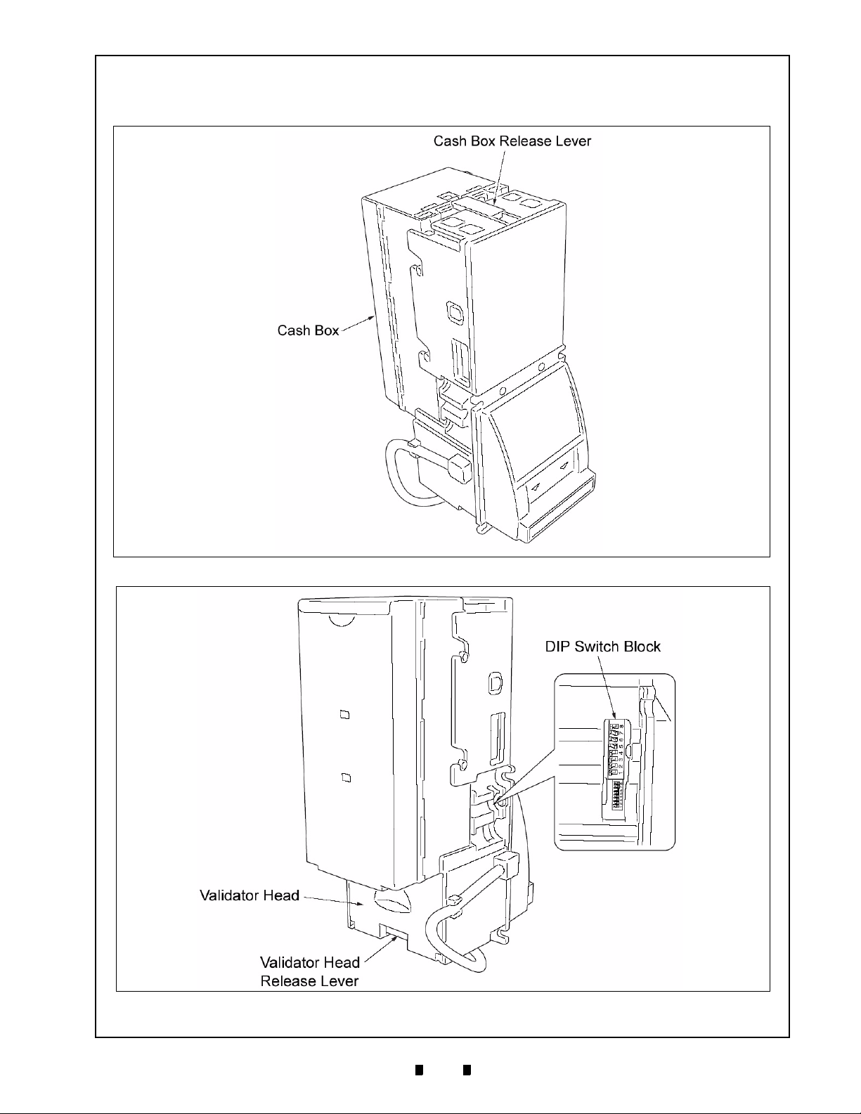
Component Names
Figure 1-3 and Figure 1-4 illustrate the primary DBV-301 component part names and locations.
Figure 1-3 Bill Validator Top and Rear View
Figure 1-4 Bill Validator Bottom and Right Side View
5900333 © 2005, JCM American, Corporation
1-3
Page 14
Section 1 Optipay™ BV General Information
General Specifications
Table 1-3: lists the general specifications for the
Titan DBV-301 Bill Validator.
Table 1-3: DBV-301 Bill Validator Specifications
N
o
1 Acceptable
MODEL SPECIFICATION
Refer to the separate “Software Specifications”
Denominations:
2 Insertion Direc-
Refer to the separate “Software Specifications”
tions:
3 Acceptance Rate: Refer to the separate “Software Specifications”
The acceptance rate will be calculated as follows:
First acceptance number of sheets + Re-insertion acceptance number of sheets
*1 = Acceptance following subsequent re-insertions
Test bill total
Note: The following bill types are excluded:
a) Bills with excessive or poor magnetism or unclear graphics
b) Double (dual) notes
c) Worn, dirty, wet, torn or excessively wrinkled bills
d) Bills having folded corners or edges
e) Bills having the wrong cut dimensions or printing displacement
4 Processing speed: Approximately 2 seconds
(time from bill insertion to credit signal output)
Approximately 3 seconds
(time from bill insertion to bill stack completion)
5 Cash box:
a) Capacity: Approximately 300 bills
b) Ejection directions: Rear ejection
*1
x 100 (%)
6 Interface: MDB interface (photo coupler isolation)
7 Escrow: 1 Bill
8 Indication:
a) Indication LED (green LED at front side)
b) Condition LEDs (green, yellow and red LEDs at rear side)
9 Power supply: 24 V DC (±5%), 2.5 A
Correspondence to an MDB interface standard power supply is possi-
ble
10Power consumption
11Environmental con-
ditions:
a) Standby status: 0.2 A
b) Operation status: 0.4 A (0.9 A maximum)
a) Operational temperature: -15 °C to 60 °C
b) Operational humidity: 15 to 95% RH (no condensing)
c) Storage temperature: -20 °C to 60 °C
d) Storage humidity: 15 to 95% RH (no condensing)
e) Light disturbance: Direct sunlight should be avoided
12Outline dimensions: 4.11 in. (104.5 mm) Width, 9.58 in. (243.5 mm) Height, 6.10 in. (155
mm) Depth (with faceplate)
13Weight: Approximately 2.64 lbs. (1.2 kg)
14Mounting: Horizontal Mounting
(verify with your sales representative prior to selecting a final attachment angle)
5900333 © 2005 JCM-American Corporation
1-4
Page 15
General Information Optipay™ BV Section 1
Retrieving Bills
1. Pull the cash box release lever in the arrow
c
direction illustrated in Figure 1-5 .
2. Lift the cash box in the
and remove it.
d
arrow direction
Figure 1-5 Initial Bill Retrieval Steps
3. Open the cash box cover in the
direction illustrated in Figure 1-6 .
e
arrow
4. Remove the bills in the f arrow direction.
Figure 1-6 Final Bill Retrieval Steps
5900333 © 2005 JCM-American Corporation
1-5
Page 16
1-6
Figure 1-7 Cable Connector Locations
Section 1 Optipay™ BV Running H/F 1
Figure 1-7 illustrates the cabling connection locations for installing the DBV--301 Bill Validator.
Cabling
5900333 © 2005, JCM American, Corporation
Page 17
Figure 1-8 Bill Validator Dimensions
1-7
Dimensions
General Information Optipay™ BV Section 1
Figure 1-8 illustrates the relative dimensions of the DBV--301 Bill Validator.
5900333 © 2005, JCM American, Corporation
Page 18

Section 1 Optipay™ BV General Information
Cash Box Label
1
2
3
10
Table 1-4: Cash Box Label Features
1. Cash Box removal
step instruction
arrows
9
8
7
2. Diagnostic LED
Flash indication
columns label
3. Diagnostic LED
column color labels
4. Note path access
step instructions
5. Note path access
step instruction
arrows
above)
(related to #4
6. column labeling
Diagnostic LED
location listings
7. Diagnostic
Description column
8. Cash Box removal
step instructions
9. JCM contact
information
10. JCM Logo.
Table 1-5: DIP Switch Label Features
1. JCM Logo 4. Arrow addressing
actual position of
DIP Switches and I/
O header connector
locations
restricted to vertical
placement positioning)
(Label is
4
Figure 1-9 Cash Box Front Label
DIP Switch Label
1
2
3
2. JCM contact
information
6
5
Figure 1-10 DIP Switch Side Label
3. Diagnostic/Inhibit
DIP Switch position
label
5. External Validatorto-vending machine
header connector
6. Interface DIP Switch
Block switch position
label.
6
5
4
5900333 © 2005 JCM-American Corporation
1-8
Page 19
General Information Optipay™ BV Section 1
Country Codes
Table 1-6: Country Codes
Country Country Code
Antilles ANT
Argentine ARG
Australia AUS
Austria AUT
Austria AUT4
Barbados BRB
Belgium BEL
Botswana BWA
Brazil BRA
Bulgaria BGR
Canada CAN
Canada CAN
Chile CHL
China CHN
Colombia COL
Costa Rica CRI
Croatia HRV
Cyprus CYP
Czech Republic CZE
Denmark DNK
Estonia ESTE
Estonia EST2
European Union EUR
Finland FIN
France FRA
Germany DEU
Germany DEU1
Germany DEU2
Germany/Sweden DEU/SWE
Great Britain (England) GBR
Table 1-6: Country Codes (Continued)
Country Country Code
Great Britain (England) GBR-B
Great Britain/Gibraltar GBR/GBI
Great Britain/Isle Of Man GBR/MAN
Greece GRC
Greece GRC-B
Guatemala MGT
Honduras HND
Hong Kong HKG
Hungary HUN
Iceland ISL
India IND
Israel ISR
Italy ITA
Italy ITA8
Italy ITA9
Japan JPN
Kazakhstan KAZ
Kazakhstan KAZ1
Latvia LVA
Lithuania LTU
Malaysia MYS
Malaysia MYS1
Malta MLT
Mauritius MUS
Mexico MEX
Moldova MDA
Morocco MAR
Namibia NAM
Netherlands NLD
Netherlands NLD-B
New Zealand NZL
5900333 © 2005 JCM-American Corporation
1-9
Page 20
Section 1 Optipay™ BV General Information
Table 1-6: Country Codes (Continued)
Country Country Code
New Zealand NZL1
New Zealand NZL-B
North Ireland NIRL
Norway NOR
Norway NOR1
Peru PER
Peru PER1
Philippines PHL
Philippines PHL1
Poland POL
Poland POL1
Poland POL1-B
Portugal PRT
Qatar QAT
Republic Of Ireland IRL
Republic Of Korea KOR
Table 1-6: Country Codes (Continued)
Country Country Code
Switzerland CHE-B
Taiwan (Republic Of
TWN
China)
Tanzania TZA
Thailand THA
Trinidad & Tobago TTO
Ukraine UKR
Ukraine UKR1
United Arab Emirates ARE
United States USA
Uruguay URY
Uruguay URY1
Venezuela VEN
Venezuela VEN1
Venezuela VEN2
Venezuela VEN-B
Republic Of Korea KOR-B
Romania ROM
Russia RUS
Russia RUS-B
Saudi Arabia SAU
Singapore SGP
Singapore SGP-B
Slovakia SVK
Slovenia SVN
South Africa ZAF
Spain ESP
Sri Lanka LKA
Sweden SWE
Switzerland CHE
Switzerland CHE3
5900333 © 2005 JCM-American Corporation
1-10
Page 21
Optipay™ BV
DBV-301 Bill Validator
Section 2
2 INSTALLATION / OPERATION
This section provides installation and operation
instructions for the Optipay
Validator. The information within contains the following features:
•
Installation
•
Input/Output Circuits
•
Pin Assignment
•
Connector
•
DIP Switch Settings
•
Operation Flowchart
•
Clearing a Bill Jam
•
Preventive Maintenance
™
BV
DBV-301 Bill
Installation
Mounting the unit
Mount the DBV-301 Bill Validator as follows:
(See Figure 2-1).
Removing the bill guide
1. Remove the faceplate and the DBV-301 Bill
Validator (i.e., reverse the “Mounting the
unit” instructions previously referenced).
2. Remove the bill guide following the arrow
c
and d directional paths indicated in Fig-
ure 2-2.
Figure 2-1 Bill Validator Mounting Locations
1. Attach the faceplate and the bill insertion
guide using four M5 hexhead screws
2. Attach the DBV-301 and its faceplate using
four M3 hexhead screws and double flat
washers
d
.
c
.
Figure 2-2 Bill Validator Removal
3. Remove the bottom bill guide following the
e
arrow
Reverse the procedure to reinstall.
direction indicated in Figure 2-3.
Figure 2-3 Bill Guide Removal
5900333 © 2005 JCM-American Corporation
2-1
Page 22

Section 2 Optipay™ BV Installation / Operation
Input/Output Circuitry
Figure 2-4 illustrates the Bill Validator-to-Controller component schematic and interconnecting pin designation diagram.
Figure 2-4 Bill Validator-to-Controller I/O Circuit and Pin-out Identification Schematic
Connector Pin Assignment
Figure 2-5illustrates the Bill Validator’s plug interconnect pin assignment diagram and Table 2-1lists each
pin’s function.
Figure 2-5 Bill Validator’s Plug Interconnect Pin Assignment Diagram
Table 2-1 Connector Pin Designations
Pin No. Signal Name I/O
1V
2V
1 DC +24 V power
DD
1Ground
SS
I/O
*
Signal Description
3 NC Not used
4 NC Not used
5 TXD1 OUT Photo coupler: output signal line from bill validator to controller
6 RXD2 IN Photo coupler: input signal line from bill validator to controller
7 SG2 Photo coupler: signal ground
8 NC Not used
9 NC Not used
10 NC Not used
11 NC Not used
12 NC Not used
13 NC Not used
14 NC Not used
15 NC Not used.
16 NC Not used
17 NC Not used
18 NC Not used.
* I/O (In/Out) viewed from the Bill Validator side.
5900333 © 2005, JCM American, Corporation
2-2
Page 23

Installation / Operation Optipay™ BV Section 2
Connector Types
•
Right Angle Dual Header
53107-1820 (MOLEX)
Polyester (w/glass inclusion)
•
Header Housing (recommended)
51030-0920 (MOLEX)
Polyester (w/glass inclusion)
•
Dual Clip
51041-1800 (MOLEX)
Polyester (w/glass inclusion)
•
Terminal
50083-8114 (MOLEX)
Wire Gauge AWG#24 ~ 26
•
Separate Wire (recommended)
UL1007 AWG#24 ~ 26
Figure 2-6 illustrates a typical interconnect plug pin configuration.
Figure 2-6 Typical Interconnect Plug Pin Assignment Diagram
DIP Switch Settings
Verify the current software in the DBV before attempting to reinstall it. The DIP switch settings are determined by the software. See software specifications provided separately for your software’s DIP switch settings. See Figure 2-7 for the DIP Switch location.
Figure 2-7 DIP Switch Location
5900333 © 2005, JCM American, Corporation
2-3
Page 24

Section 2 Optipay™ BV Installation / Operation
Operational Flowchart
Figure 2-8 depicts a typical bill acceptance flow process.
Figure 2-8 Bill Validator Operational Flowchart
5900333 © 2005, JCM American, Corporation
2-4
Page 25

Installation / Operation Optipay™ BV Section 2
Clearing a Bill Jam
When a bill is jammed in the Stacker section:
1. Remove the cash box.
2. Remove the jammed bill following the arrow
path shown in Figure 2-9.
Preventive Maintenance
The DBV-301 sensor lenses c are made of a transparent polymer material; handle them with care. It
is important to keep the bill path, rollers
belts clean (See Figure 2-11, and Figure 2-12 for
locations).
d
, and
Figure 2-9 Clearing a Jammed Stacker Bill
When a bill is jammed in the Validator
section:
1. Lift the Validator head release lever and pull
out the Lower Guide.
2. Remove the jammed bill.
Figure 2-11 Upper Guide and Stacker
Sensors and Rollers
Figure 2-12 Lower Guide Sensors and Rollers
Figure 2-10 Clearing a Jammed Validator
5900333 © 2005 JCM-American Corporation
To clean the lenses, use a lint-free cloth and a mild
non-abrasive detergent such as liquid dish soap
mixed with water.
2-5
Page 26

Section 2 Optipay™ BV Installation / Operation
Do not use alcohol or thinner for
cleaning.
Note: JCM does not recommend using
cleaning cards, cleaning pads, or cleaning
solutions of any kind
.
Cash box Preventive Maintenance (P/M)
Perform periodic P/M on the Cash Boxes to ensure
proper operation. The Cash Box sensor lenses
are made of a transparent polymer material; handle
them with care (See Figure 2-13).
c
Figure 2-13 Cash Box Sensors
Use compressed air to blow out loose paper fibers
and other debris that can build up over time. Check
all moving parts for wear and proper positioning. If
the unit does not operate properly, it can cause bill
jams. After completing the P/M, re-calibration is
recommended (Refer to Section 7).
5900333 © 2005 JCM-American Corporation
2-6
Page 27

3 MDB PROTOCOL
NOTE: The latest MDB Protocol Specifications may be found at www.Vending.org
Optipay™ BV
DBV-301 Bill Validator
Section 3
5900333 © 2005 JCM-American Corporation
3-1
Page 28

Optipay™ BV
THIS PAGE INTENTIONALLY LEFT BLANK
5900333 © 2005 JCM-American Corporation
3-2
Page 29

Optipay™ BV
DBV-301 Bill Validator
Section 4
4 DISASSEMBLY
This section provides disassembly instructions for
the Optipay
information within contains the following features:
1. Circuit Board Disassembly
2. Pusher Mechanism Disassembly
3. Upper Guide Disassembly
4. Lower Guide Disassembly
Circuit Board Disassembly
Removing the CPU and Power Supply
boards
1. Pull the cash box release lever c and
™
BV
DBV-301 Bill Validator. The
remove the cash box
d
(See Figure 4-1).
Figure 4-2 Lower Guide Removal
Figure 4-1 Bill Validator Mounting Locations
2. Lift the Validator head release lever and pull
out the Lower Guide following the arrow
and directional path indicated in Figure 4-2.
3. Slide the base cover upward and remove the
cover (See Figure 4-3).
4. Remove four securing screws and remove
the face plate (See Figure 4-4 and
Figure 4-5).
5900333 © 2005 JCM-American Corporation
Figure 4-3 Validator Cover Removal
Figure 4-4 Validator Face Plate Removal
4-1
Page 30

Section 4 Optipay™ BV Disassembly
Figure 4-5 Face Plate Rear Mounting View
5. Lay the assembly on its back and remove the
6 screws shown in Figure 4-6. Then disconnect the four plug connectors indicated by
the four small arrows in Figure 4-6.
6. Open the board assembly access box following the large arrow direction in Figure 4-6.
Figure 4-7 CPU Board Connector Removals
9. Separate the CPU board and Power Supply
board connectors (See Figure 4-8)
.
Small
Arrows
Figure 4-6 Screw and Connector Removal and
Circuit Board Access
7. Release the ribbon cable connector lock and
remove the flexible ribbon cable shown by
the small arrows in the Figure 4-7 close-up
box (See Figure 4-7 a).
8. Disconnect the CPU board signal cable connector (See large arrow in Figure 4-7 b).
Figure 4-8 CPU and Power Supply Board
Connector Separation
5900333 © 2005 JCM-American Corporation
4-2
Page 31

Disassembly Optipay™ BV Section 4
Pusher Mechanism Disassembly
Timing Belt removals
1. Remove the CPU board and power supply
board as previously described (See “Removing the CPU and Power Supply boards” on
page 4-1).
2. Remove the Side Bill Guides by following
the
c
and d arrow directions shown in
Figure 4-9.
Figure 4-9 Side Guide Removal
3. Remove the Front Bill Guide following the
large directional arrow shown in Figure 4-
10.
Figure 4-10 Front Guide Removal
4. Remove the pusher mechanism retaining
screw and remove the assembly following
the large directional arrow shown in
Figure 4-11.
Figure 4-11 Pusher Mechanism Removal
5. Remove the two timing belts from the
Pusher Mechanism assembly
(See Figure 4-12). Once the belts are
removed, remove their related tension rollers
on each side as well (See Figure 4-12 a).
Figure 4-12 Timing Belt Removal
Removing the drive and stack motor
1. Remove the two shaft retaining C-clip rings
and pull the shaft out of the pusher plate
(See Figure 4-13).
5900333 © 2005 JCM-American Corporation
4-3
Page 32

Section 4 Optipay™ BV Disassembly
Figure 4-15 Shaft and Sleeve Removal
Figure 4-13 Pusher Shaft C-Clip Ring Removal
2. Slide the pusher plate in the direction indicated by the arrow in Figure 4-14 and
remove the plate.
Figure 4-14 Pusher Plate Removal
3. Remove one of the shaft retaining C-clip
rings and pull the shaft out of the pusher
arm; then remove the two sleeve spacers
(See Figure 4-15).
4. Lift the pusher arm and remove the five
retaining screws shown in Figure 4-16, then
tip the assembly to the side and remove the
loose pin (See Figure 4-16 a).
5. Turn the Pusher Mechanism assembly over
and remove the motor guide
(See Figure 4-17).
Figure 4-16 Retaining Screw Removals
Figure 4-17 Motor Guide Removal
5900333 © 2005 JCM-American Corporation
4-4
Page 33

Disassembly Optipay™ BV Section 4
6. Remove the drive and stack motor from the
motor guide assembly (See Figure 4-18).
Figure 4-18 Drive and Stack Motor Removal
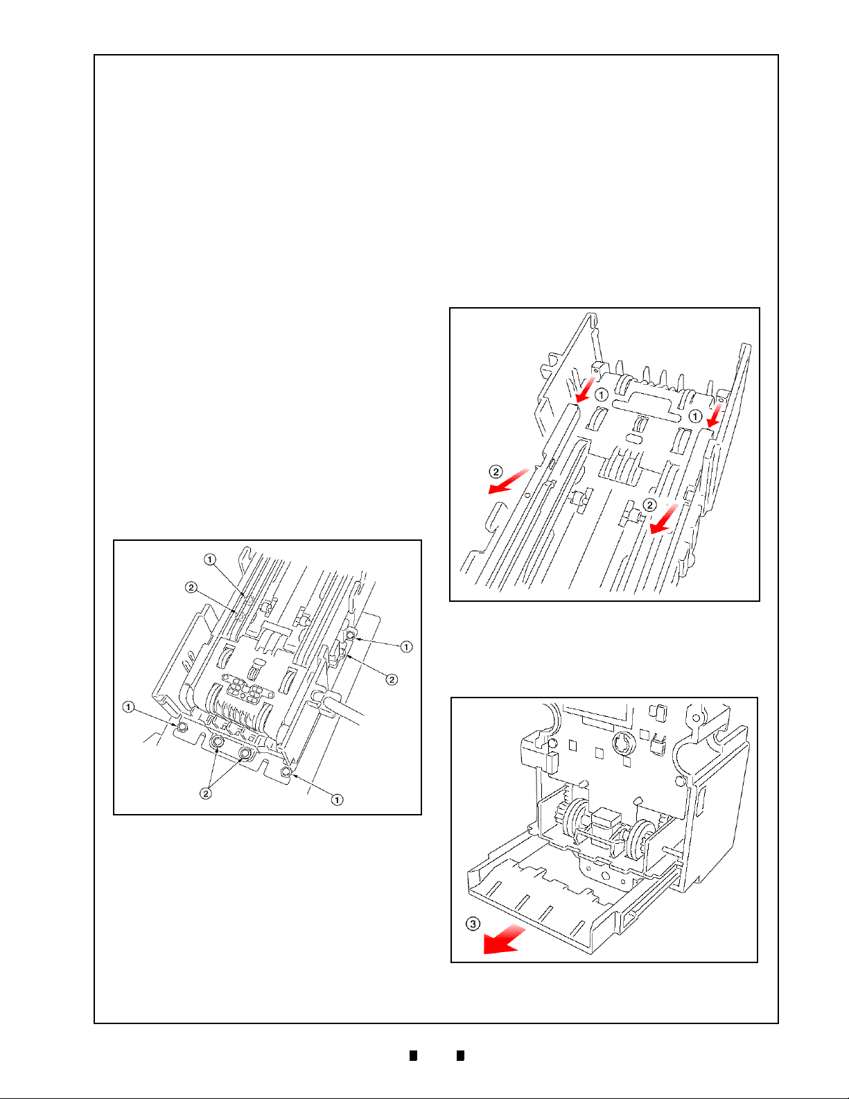
Upper Guide Disassembly
3. Pull the two shafts out and remove the two
small and two large gears (See Figure 4-20).
Figure 4-20 Upper Guide Gear Removals
4. Remove the two retaining Sensor board
screws and remove the Sensor board from
the assembly (See Figure 4-21).
Sensor board removal
1. Remove the Pusher Mechanism assembly
(See “Pusher Mechanism Disassembly” on
page 4-3).
2. Remove the two Upper Guide retaining
screws and pull the Upper Guide out of the
assembly (See Figure 4-19).
Figure 4-21 Sensor Board Removal
5. Release the ribbon cable connector lock and
remove the flexible ribbon cable from the
Sensor board (See Figure 4-22 arrows).
Figure 4-19 Upper Guide Removal
5900333 © 2005 JCM-American Corporation
Figure 4-22 Flexible Ribbon Cable Removal
4-5
Page 34

Section 4 Optipay™ BV Disassembly
O-ring removal
1. Pull the two short gear shafts out and remove
the two gears they retained (See Figure 4-
23).
Figure 4-25 Upper Long Shaft and Gear Removal
Figure 4-23 Short Shaft and Gear Removal
2. Pull the lower long gear shaft out and
remove the two gears it retained (See Figure
4-24).
Figure 4-24 Lower Long Shaft and Gear Removal
3. Pull the upper long gear shaft out and
remove the two gears, springs and bushings
it retained (See Figure 4-25)
4. Remove the two concentric O-rings from
each gears just removed from the upper shaft
assembly (See Figure 4-26).
Figure 4-26 O-Ring Removals
Lower Guide Disassembly
MAG board removal
1. Remove the Lower Bill Guide retaining
screw and remove the Lower Bill Guide’s
cover following the large arrow direction
shown in Figure 4-27
.
5900333 © 2005 JCM-American Corporation
Figure 4-27 Lower Bill Guide Removal
4-6
Page 35

Disassembly Optipay™ BV Section 4
2. Remove the two screws retaining the MAG
board to the assembly and lift the MAG
board (See Figure 4-28).
Figure 4-28 MAG Board Removal
3. Disconnect the board connector and remove
the MAG board (See Figure 4-29).
Figure 4-29 Disconnect MAG Board Connector
5900333 © 2005 JCM-American Corporation
4-7
Page 36

Optipay™ BV
THIS PAGE INTENTIONALLY LEFT BLANK
5900333 © 2005 JCM-American Corporation
4-8
Page 37

Optipay™ BV
DBV-301 Bill Validator
Section 5
5 WIRING DIAGRAMS
This section provides the Wiring Diagram interconnect for the Optipay
dator (See Figure 5-1 and Figure 5-2).
™
BV
DBV-301 Bill Vali-
DBV-301 Interconnect
This section contains the following information:
1. DBV-301-SU Interconnect (Part 1)
2. DBV-301-SU Interconnect (Part 2)
Figure 5-1 DBV-301 Bill Validator Interconnect Wiring Diagram (Part 1)
5900333 © 2005 JCM-American Corporation
5-1
Page 38

Section 5 Optipay™ BV Wiring DiagramS
DBV-301 Interconnect Continued
Figure 5-2 DBV-301 Bill Validator Interconnect Wiring Diagram (Part 2)
5900333 © 2005, JCM American, Corporation
5-2
Page 39

Optipay™ BV
DBV-301 Bill Validator
Section 6
6 TROUBLE SHOOTING
This section provides the Trouble Shooting
procedures for the Optipay
Validator. The information within contains the
following features:
•
DBV-301-SU
Trouble Shooting
™
DBV-301 Bill
Introduction
Most failures within the Bill Validator occur due to
minor causes. It is important to check that the internal connectors are properly mated and that the harness is also firmly connected before replacing
parts.
Poor bill acceptance is often due to iron content
that adheres to the magnetic head or to the magnetic head roller. Therefore, the Bill Validator
should always be cleaned first.
To determine the cause of a failure and those of
small defective parts, it is important to observe the
operating state of the Bill Validator when power is
first applied. This condition also allows the cause
of a failure to be determined using the test mode.
When the Bill Validator head has been disassembled for repair, or when the Sensor board has been
replaced, the sensor should be readjusted.
All repairs should be performed by referring to the
adjustment procedure, the wiring diagrams and the
various disassembly procedures.
Failure Classifications
The cause of a failure can be broadly classified into
the following four failure conditions. Check for the
following operating fault states:
1. Test mode fails entry (See Figure 6-1and 2).
2. Incorrect initial operation (See Figure 6-3).
3. Rejected or poorly accepts bills (See Figure
6-4).
4. Improper bill transfer (See Figure 6-5).
Test Mode Entry Failure Flowchart
The Figure 6-1 and 2 Flowcharts diagram the failure conditions related to entering test correctly.
Figure 6-1 DBV-301 Bill Validator Test Mode Failure Flow Chart Diagram (Part 1)
5900333 © 2005 JCM-American Corporation
6-1
Page 40

Section 6 Optipay™ BV Trouble Shooting
Test mode entry failure flowchart (continued)
Figure 6-2 DBV-301 Bill Validator Test Mode Failure Flow Chart Diagram (Part 2)
5900333 © 2005, JCM American, Corporation
6-2
Page 41

Trouble Shooting Optipay™ BV Section 6
Incorrect initial operation flowchart
The Figure 6-3 Flowchart diagrams the LED indications available when an incorrect initial operational
fault occurs.
Figure 6-3 DBV-301 Bill Validator Incorrect Initial Operation Flow Chart Diagram
5900333 © 2005, JCM American, Corporation
6-3
Page 42

Section 6 Optipay™ BV Trouble Shooting
Rejected or poorly accepts bills flowchart
The Figure 6-4 Flowchart diagrams the fault conditions related to Bill Validator rejects or poorly accepts
bills.
Figure 6-4 DBV-301 Bill Validator Rejects or Poorly Accepts Bills Flow Chart Diagram
5900333 © 2005, JCM American, Corporation
6-4
Page 43

Trouble Shooting Optipay™ BV Section 6
Improper bill transfer flowchart
The Figure 6-5 Flowchart diagrams the fault conditions related to Improper bill transfers.
Figure 6-5 DBV-301 Bill Validator Improper bill transfer Flow Chart Diagram
5900333 © 2005, JCM American, Corporation
6-5
Page 44

Optipay™ BV
THIS PAGE INTENTIONALLY LEFT BLANK
5900333 © 2005 JCM-American Corporation
6-6
Page 45

Optipay™ BV
DBV-301 Bill Validator
Section 7
7 FLASH MEMORY DOWNLOAD
This section provides download instructions for the
Optipay™
mation within contains the following
features:
•
•
•
•
•
•
•
•
•
•
•
BV
DBV-301 Bill Acceptor. The infor-
Downloading to Flash Memory Description
Tool Requirements
Information Menu Selection
Diagnostics Menu Selection
Program Download Menu Selection
Selecting a Download ROM
Starting the Download Program
Downloading Procedure Examples
DIP Switch Settings
Error Codes
Sensors, Circuit Boards, and Motor Locations
a
Tool Requirements
A Palm Pilot® handheld device is required to
configure the DBV-301 Bill Acceptor using JCM
PSP-03
Requirements
©
Acceptor Program software.
•
A Palm Pilot Handheld – M100, 500 and
Tungsten Series Handhelds (See Figure 7-1 )
•
Titan Acceptor Communication Cable
•
JCM PSP-03 Acceptor Program for the
Palm Pilot handheld
•
PC with Windows 2000 or XP O/S
•
Palm Pilot Application Suite
•
Hot Sync Cradle or Cable*
*Refer to the Palm Pilot User’s manual
for program installation and Hot Sync
instructions.
Figure 7-1 Typical M100/500 Series Palm
®
Handheld & Software
Pilot
Information Menu Selection
1. Turn on the Palm Pilot® and select the JCM
PSP-03 main menu application (See Figure
7-1 a or See Figure 7-2 a).
a
Figure 7-2 PSP-03 Application Selection
2. Select the
main menu screen
(See Figure 7-3 a).
Settings
button on the
5900333 © 2005 JCM-American Corporation
7-1
Page 46

Section 7 Optipay™ BV Flash Memory Download
3. Select the
Information…
button on the
menu screen. (See Figure 7-4 a)
or
Back
to return to the previous screen.
a
Figure 7-3 Settings Menu Selection
a
5. Once back on the
Acceptor…
the
button (See Figure 7-6 a).
“Settings”
screen, select
a
Figure 7-6 Acceptor Mode Selection
With future firmware releases, the
screen will be used to configure the Bill
Validator settings as well (See Figure 7-7 ),
for the present however, select
Back
return to the main menu screen.
to
Figure 7-4 Information Menu
Selection
4. The following typical configuration settings
for a validator are shown in Figure 7-5
when the
“Information…”
button is selected:
a. The Firmware Version – V1.02C
b. The Enable/Disable DIP Switch Settings
c. The bill values enabled ($1 and $5 Bills)
d. The
“Rec”
button to enter refreshed data
from the Validator and
e. The
“Back”
“Settings”
button to return to the
Screen.
a
b
c
d
e
Figure 7-7 Acceptor Screen Functions
6. Once on the
Back
the
main menu screen
button again to return to the
menu screen, select
(See Figure 7-8 ).
Figure 7-8 Returning to the Settings Screen
Figure 7-5 Typical Configuration Settings
5900333 © 2005 JCM-American Corporation
7-2
Page 47

Flash Memory Download Optipay™ BV Section 7
Diagnostics Menu Selection
7. On the
screen select the
(See Figure 7-9 a).
a
Figure 7-9 Diagnostics Mode Selection
8. The screen is used to test
the following DBV functions:
a. Forward Motor Speed RPM
b. Reverse Motor Speed RPM
c. Stacker Test
d. Run Test
e. Solenoid Test
f. Sensor 1 Transmit/Receive Test
g. Sensor 2 Transmit/Receive Test
h. Dip Switch Settings Test
Diagnostics
main menu
button
(See Figure 7-10 “a” through “h”)
Program Download Menu Selection
1. Select the
main menu screen
(See Figure 7-11 a).
a
Figure 7-11 Program Download Menu Selection
2. Select the software version to be downloaded (See Figure 7-12 a), and then
3. Select
Validator (See Figure 7-12 b).
a
Program Download
Send
to transmit the software to the
button on the
Figure 7-10 Diagnostics Screen Functions
9. Select the
Back
button to return to the
menu screen.
a
b
b
c
d
e
f
g
h
Figure 7-12 Program Download Screen
NOTE: The
loaded firmware version. To select from the
available versions loaded, mouse-click any
open area inside of the
Rom Name:
box shows the
Rom Name:
box.
Selecting a Download ROM
Having mouse-clicked any open area inside of the
Rom Name:
1. Select the firmware version from the
2. Click the
box:
available list on the
screen that
appears (See Figure 7-13 a), then
Back
button to return to the
main menu screen (See
Figure 7-13 b).
5900333 © 2005 JCM-American Corporation
7-3
Page 48

Section 7 Optipay™ BV Flash Memory Download
3. Select
Send
on the
main menu to start the selected firmware
download (See Figure 7-15 a).
a
b
Figure 7-13 ROM Select Screen
4. During the download incrementing numbers
will appear in an inset
window left of the correct final value shown
at right (See Figure 7-14 a).
b
a
Figure 7-15 Download Send Command
Accepting Log Menu Selection
1. On the
screen, select the
button (See Figure 7-16 ).
Accepting Log
c
main menu
menu
a
Figure 7-14 Download Transfer Screen
NOTE: Ensure that the number of data
bytes loaded versus the total data bytes
needed to complete the download process
agree when the download is complete (i.e.,
a = b in Figure 7-14 ).
b
5. Once the download is complete, verify that
the program version listed on the
Download”
screen agrees with your initial
“Program
selection (See Figure 7-15 b).
6. Click the
Back
button to return to the on the
main menu screen
(See Figure 7-15 c).
a
Figure 7-16 Accepting Log Mode Selection
2. In the
a.
Rec
b.
Init
to download the
to initialize or clear the validator
menu choose:
Accepting Log
memory
Del
c.
to clear all downloaded Accepting
Logs, or
d.
Back
to return to the
3. Click on the
main screen of Figure 7-16 .
download record number
itself to view the related log data (See
Figure 7-18 a). The
screen
illustrated in Figure 7-19 will then appear.
4. Select
Next
to view additional pages of the
selected (See Figure 7-19 )
5900333 © 2005 JCM-American Corporation
7-4
Page 49

Flash Memory Download Optipay™ BV Section 7
b
a
Figure 7-17 Accepting Log Menu
c
d
a
Figure 7-18 Viewing Record Log Data
a
Figure 7-19 Viewing Specific Log Data 1
5. .Page two of the
lists the last
16 bills accepted, their denomination and the
direction in which the bill was inserted
(See Figure 7-20 ).
6. Page three lists the total bill denominations
counted and their date code, those accepted
and those rejected as follows:
a. The specific bill type count
b. The denomination and its sort date code
(Example 1 = 1$ of series 1990, 87 bills
accepted, 0 rejected)
a
Figure 7-20 Viewing Page Two Log Data
c. The number of the specific bills accepted
d. The number of the specific bills rejected
(See Figure 7-21 a, b, c, and d respectively)
b
a
Figure 7-21 Viewing Page Three Log Data
c
d
7. Page four, shown in Figure 7-22 , lists the
following information from top to bottom:
a.
RC Bills:
Number of bills stored in the
Recycler
–
(the amount operator loaded plus
customer loaded) minus the (amount
operator dispensed plus customer
dispensed)
b.
BOX STK:
Number of bills stacked in the
Cash Box
–
(the amount of notes stacked during
customer operation) plus (amount of
notes stacked during a manual RC-10
stacking operation)
c.
Recycle Operation:
Number of bills
loaded by operation mode
–
the amount of bills dispensed from the
RC-10 during a normal customer
transaction
d.
Manual:
= Number of bills loaded manu-
ally
5900333 © 2005 JCM-American Corporation
7-5
Page 50

Section 7 Optipay™ BV Flash Memory Download
b
d
f
h
j
l
Figure 7-22 Viewing Page Four Log Data
–
the amount of bills loaded into the
RC-10 by using the manual load
function
e.
Payout Operation:
Number of bills dis-
pensed by using the operation mode
–
the amount of bills dispensed from
RC-10 during a normal customer
transaction
Manual:
f.
Number of bills dispensed by
manual
–
the amount of bills dispensed from
RC-10 by using the manual dispense
function
g.
Gather:
Number of bills dispensed to
Cash Box
–
the amount of bills dispensed from
RC-10 to the Cash Box during a
manual dispense function
h.
Empty:
Number of times the Recycler
was empty
i.
FULL:
Number of times the Recycler
became FULL
Abnormal:
j.
Number of times the Recycler
had trouble (including bill jams)
Rec STK:
k.
a
c
e
g
i
k
DIP Switch Settings
Test mode set-up
To enter the test mode, set the following DIP
switches to:
stacked in the Cash Box during loading
l.
Pay STK:
stacked in the Cash Box when dispensing.
Number of bills mandatory
Number of bills mandatory
1. Turn switch 8 ON, turn switches 1 to 7 OFF,
and supply power to the unit.
2. The Faceplate LEDs will blink and the
Green, Yellow and Red Status LED indicator
on the rear of the unit will illuminate (turn
ON).
3. Keep switch 8 ON, then
4. Set switches 1 through 7 according to the test
mode you wish to conduct.
5. Now turn switch 8 OFF to begin the selected
test.
The Faceplate LEDs will go out along with
the Green, Yellow and Red LED Status
indicator LEDs located on the rear of the
unit.
6. Turn switch 8 ON to finish the test.
The Faceplate LEDs will blink and the
Green, Yellow and Red Status LED indicator
on the rear of the unit will illuminate (turn
ON).
Setting the test mode switches
Column 1 of Table 7-1 lists the various DIP
Switch Block settings for activating the desired
tests chosen from the “
listed in Column 2 of Table 7-1 .
Test Mode Descriptions”
Table 7-1 DIP Switch 1 Test Mode Settings
DIP Switch 1
No. 1 2 3 4 5 6 7 8
Transport Motor Forward Rotation Test (BOX set)
1) Normal: Status LEDs (Green, Yellow & Red) blink once
2) Fast: Status LEDs (Green, Yellow & Red) blink twice
3) Slow: Status LEDs (Green, Yellow & Red) blink 3 times
4) Abnormal: Status LEDs (Green, Yellow & Red) blink 6 times
Transport Motor Reverse Rotation Test (BOX set)
1) Normal: Status LEDs (Green, Yellow & Red) blink once
2) Fast: Status LEDs (Green, Yellow & Red) blink twice
3) Slow: Status LEDs (Green, Yellow & Red) blink 3 times
4) Abnormal: Status LEDs (Green, Yellow & Red) blink 6 times
5900333 © 2005 JCM-American Corporation
Test Mode Description
7-6
Page 51

Flash Memory Download Optipay™ BV Section 7
Table 7-1 DIP Switch 1 Test Mode Settings (Continued)
DIP Switch 1
No. 1 2 3 4 5 6 7 8
Test Mode Description
Stacker Test (BOX set)
1) Normal: Status LEDs all OFF
2) Stacker FULL: Status LED (Yellow) blinks once
3) Stacker JAM/LOCK: Status LED (Red) blinks twice
4) Box error: Status LED (Yellow) blinks 10 times
Running Test (BOX set)
1) Normal: Status LEDs all OFF
2) Stacker FULL: Status LED (Yellow) blinks once
3) Stacker JAM/LOCK: Status LED (Red) blinks twice
4) Acceptor JAM: Status LED (Yellow) blinks 4 times
5) Motor SPEED: Status LED (Red) blinks 5 times
6) Motor LOCK: Status LED (Red) blinks 6 times
7) BOX Error: Status LED (Yellow) blinks 10 times
Serial Insertion Prevention Lever Test
1) Normal: Status LEDs all OFF
2) Sensor ABN: Status LED (Green, Yellow & Red) 4 blinks each
3) Motor LOCK: Status LED (Green,Yellow & Red) 6 blinks each
Acceptor Sensor Test
[Refer to details concerning the Acceptor Sensor Test in Table 7-2]
Stacker Sensor Test
[Refer to details concerning the Stacker Sensor Test in Table 7-3]
Acceptance Test (BOX set)
Stack Motor Forward Rotation Test (pusher plate remains at HOME position)
1) Normal: Status LEDs (Green, Yellow & Red) 1 blink each
2) Fast: Status LEDs (Green, Yellow & Red) 2 blinks each
3) Slow: Status LEDs (Green, Yellow & Red) 3 blinks each
4) Abnormal: Status LEDs (Green, Yellow & Red) 6 blinks each
Stack Motor Reverse Rotation Test (pusher plate remains at HOME position)
1) Normal: Status LEDs (Green, Yellow & Red) 1 blink each
2) Fast: Status LEDs (Green, Yellow & Red) 2 blinks each
3) Slow: Status LEDs (Green, Yellow & Red) 3 blinks each
4) Abnormal: Status LEDs (Green, Yellow & Red) 6 blinks each
I/O Pulse Interface Line Test
1) InLine1 (Low: OutLine1 = Low, Hi: Outline1 = Hi)
2) InLine2 (Low: OutLine2 = Hi, Hi: Outline2 = Low)
3) InLine3 (Low: OutLine3 = Hi, Hi: Outline3 = Low)
4) 500md Interval: OutLine4 = Hi/Low
DIP Switch Test
[Refer to details concerning the DIP Switch Test in Table 7-4 on page 7-9]
5900333 © 2005 JCM-American Corporation
7-7
Page 52

Section 7 Optipay™ BV Flash Memory Download
Test Mode Details
Acceptor Sensor Test Details
When a bill is inside the unit, the Faceplate LEDs and the Green, Yellow and Red Status LEDs Illuminate
(turn ON).
NOTE: Multiple sensors can be tested simultaneously.
Table 7-2 Acceptor Sensor Test Detail Listing
No. 1 2 3 4 5 6 7 8 Sensor Name
LEV (Serial Insertion Prevention Lever)
PSF (f0t_ir: Entrance)
PSML (l1t_rd: RED Left 1)
PSMR (r1t_rd: RED Right 1)
PSL (l3t_ir: Infrared Left 3)
PSR (r3t_ir: Infrared Right 3)
PSE (ext_ir: Exit)
Stacker SensorTest Details
When a bill is inside the unit, the Faceplate LEDs and the Green, Yellow and Red Status LEDs Illuminate
(turn ON).
NOTE: All sensors must be tested individually.
Table 7-3 Stacker Sensor Test Detail Listing
No. 1 2 3 4 5 6 7 8 Sensor Name
PSL (Transport Unit Left Sensor detects a bill)
Reversed
PSR (Transport Unit Right Sensor detects a bill)
HOME (pusher plate is at HOME position)
BOX (Cash Box is in proper position)
Stack Motor Encoder (when shielded)
5900333 © 2005, JCM American, Corporation
7-8
Page 53

Flash Memory Download Optipay™ BV Section 7
Table 7-3 Stacker Sensor Test Detail Listing (Continued)
No. 1 2 3 4 5 6 7 8 Sensor Name
Transport Motor Encoder (when shielded)
DIP Switch Logic Test
Test results are indicated by making the following switch settings and observing the Condition LED blinking indications listed in the Table 7-4 tests:
1. Begin by setting DIP Switch 1 Block switches 1 through 8 all ON, and apply power to the unit.
The Front Panel Green Indicator LEDs will begin flashing and the Green, Yellow and Red Condition
LEDs will all steadily illuminate (lite).
2. Now change DIP Switch 1 Block switch number 8 to OFF. The Front Panel Green Indicator LEDs
will go out and the Green, Yellow and Red Condition LEDs will all begin to repeatedly blink single
flashes (See Table 7-4 Test 1).
3. Now turn DIP Switch Block 2 switches 1 through 8 all ON. The Front Panel Green Indicator LEDs
will remain out and the Green, Yellow and Red Condition LEDs will begin repeatedly blinking
in double flash sets (See Table 7-4 Test 2).
4. Now turn even numbered switches (i.e., 2, 4 & 6) on both DIP Switch Block 1 and
Block 2 OFF. The Green, Yellow and Red Condition LEDs will then begin repeatedly blinking three
flashes at a time. (See Table 7-4 Test 3).
DIP Switch
Table 7-4 Resulting DIP Switch Setting LED Flash Details
Test
No.
1 Condition LEDs Blink once (1 time)
2 Condition LEDs Blink twice (2 times)
3 Condition LEDs Blink three times (3
DIP Switch 1
No. 1 2 3 4 5 6 7 8
DIP Switch 2
No. 1 2 3 4 5 6 7 8
Condition LED Blink Indications
times)
Error Codes
Error Code Table
Table 7-5 lists the color error code and number of blinks for each test result.
Table 7-5 Error Code Blink Listing
Blink Number LED Color Status Error Description
1 Yellow Stacker Full
2 Red Stacker Jam (in pusher mechanism zone)
3 Yellow Acceptor Jam (in sensor zone)
4 Yellow Transport Jam
5 Red Motor Speed Error
6RedMotor Lock
5900333 © 2005, JCM American, Corporation
7-9
Page 54

Section 7 Optipay™ BV Flash Memory Download
Table 7-5 Error Code Blink Listing (Continued)
Blink Number LED Color Status Error Description
7 — Reserved (unused)
8 — Reserved (unused)
9 Yellow Entrance Lever Jam
10 Yellow BOX not Secure in Position
11 — Reserved (unused)
12 Yellow Tampering (bill fishing, bill movement incorrect, etc.)
13 — Reserved (unused)
14 — Reserved (unused)
15 Red EEPROM Read/Write Error
Reject Code Table
Table 7-6 lists the reject code and number of blinks for each test result.
Table 7-6 Reject Code Listing
Blink Number LED Color Status Code Reject Description
1 Green RJ_SLA Insertion Error
2 Green RJ_MAG Magnetic Error
3 Green RJ_PAP Particle Matter in the Transport Path
4 Green RJ_XRT Correction Error/Scaling Error
5 Green RJ_SYN Transport Error
6 Green RJ_PTO Bill Denomination Identification Error
7 Green RJ_PIR Photo Pattern Error (1)
8 Green RJ_PHV Photo Level Error
9 Green RJ_INH Inhibited Denomination
10 Green RJ_REJ Reject Command Activation
11 Green RJ_LVR Exit Sensor Error (foreign particle detected)
12 Green RJ_BSW Escrow Position Error
13 Green RJ_LGO Bill Length Error
14 Green RJ_2CL Photo Pattern Error (2)
15 Green RJ_FAKE Bill inserted does not match the genuine note
characteristics
5900333 © 2005, JCM American, Corporation
7-10
Page 55

Flash Memory Download Optipay™ BV Section 7
Sensors, Circuit Boards, Motors and Cash Box Locations
Figure 7-23 Sensors, Circuit Boards, and Motor Locations Diagram
5900333 © 2005, JCM American, Corporation
7-11
Page 56

Optipay™ BV
THIS PAGE INTENTIONALLY LEFT BLANK
5900333 © 2005 JCM-American Corporation
7-12
Page 57

Optipay™ BV
DBV-301 Bill Validator
Section 8
8 EXPLODED VIEWS/PARTS LISTS
This section provides the following wiring diagrams for theOptipay™
Validator (See Figure 8-1through Figure 8-4).
•
DBV Primary Component Parts
•
Frame and Upper/Lower Guide Exploded
View
DBV Primary Component Parts
BV DBV-301 Bill
•
Frame and Upper/Lower Guide Parts List
•
Pusher Mechanism Assembly Exploded View
•
Pusher Mechanism Assembly Exploded View
Parts List
•
Cash Box Unit Exploded View
•
Cash Box Unit Parts List
5900333
Figure 8-1 DBV Dual Bill Validator Primary Component Parts Exploded View Diagram
© 2005 JCM-American Corporation
8-1
Page 58

Section 8 Optipay™ BV Exploded Views/Parts Lists
DBV Primary Parts List
Table 8-1
No. EDP No. Part No. Description Remarks
1 095379 3210-05-03 MDB Connector
DBV Primary Parts List
Frame and Upper/Lower Guide Exploded View
5900333
Figure 8-2 Frame and Upper/Lower Guide Exploded View Diagram
© 2005, JCM American, Corporation
8-2
Page 59

Exploded Views/Parts Lists Optipay™ BV Section 8
Frame and Upper/Lower Guide Parts List
Table 8-2: Frame and Upper/Lower Guide Parts List
No. EDP No. Part No. Description Remarks
101 095517 4019GE0103 GEAR C
102 094010 4019-3210-06-03C-01 SENSOR PCB ASSY
103 095378 FFC28PIN 60MM FLEXIBLE HARNESS
104 095472 4019RE0102 UPPER GUIDE
105 095523 4019RO0101 ROLLER A
106 066077 0643CS0102A TRANSPORT ROLLER SP
107 095478 4019RE0107 ROLLER GUIDE B
108 095477 4019RE0106 ROLLER GUIDE A
109 095532 4019SH0103 ROLLER SHAFT B
110 095531 4019SH0102 ROLLER SHAFT A
111 095485 4019RE0114 SENSOR GUIDE C
112 095483 4019RE0112 SENSOR GUIDE A
113 100448 4019CS0101 LEVER SPRING
114 101151 Z3240-6115 PBT BUSHING
115 095481 4019RE0110 LEVER
116 095515 4019GE0101 GEAR A
117 095516 4019GE0102 GEAR B
118 094209 4019-3210-06-02D-01 MAG PCB ASSY
119 095377 3210-05-01A HARNESS
120 095474 4019RE0103 LOWER GUIDE
121 075183 C-125 SPRING (NO.1024)
122 101904 DC-158 SPRING
123 095479 4019RE0108 ROLLER GUIDE C
124 095524 4019RO0102 ROLLER B
125 092230 2X12 PARALELL PIN
126 095530 4019SH0101 LOCK SHAFT
127 003707 C-CLIP Φ3 SUS
128 064533 C-147 SPRING (NO.1052)
129 095476 4019RE0105 LOWER GUIDE COVER
130 094012 4019-3210-06-05-01 SMALL PCB ASSY
131 095380 3210-05-06B TRANSPORT HARNESS (Left)
132 095381 3210-05-07 TRANSPORT HARNESS (Right)
133 095471 4019RE0101 BASE FRAME
134 095482 4019RE0111 BOX STOPPER
135 095880 DC-097 SPRING
136 095505 4019RE0401 FACE PLATE
137 095506 4019RE0402 LEDGUIDE
138 095529 4019PT0401 FP BRACKET
5900333
© 2005, JCM American, Corporation
8-3
Page 60

Section 8 Optipay™ BV Exploded Views/Parts Lists
Table 8-2: Frame and Upper/Lower Guide Parts List (Continued)
No. EDP No. Part No. Description Remarks
139 094138 4019-3210-06-01D-01 CPU PCB ASSY
140 095376 LSEP1114A1 POWER SUPPLY ASSY
141 095507 4019RE0403 FB GUIDE-67
142 095508 4019RE0404 SB GUIDE-67L
143 095509 4019RE0405 SB GUIDE-67R
144 095475 4019RE0104 BASE COVER
145 095876 0-RING P-16 (EPDM70)
146 095484 4019RE0113 SENSOR GUIDE B
147 101906 4019PE0103 SG REFLECTOR SEAL
148 095480 4019RE0109 ROLLER GUIDE D
149 095533 4019SH0104 ROLLER SHAFT C
150 072396 0666RE0126A PRISM GUIDE
151 055413 2.6X6 BINDING P TIGHT
152 005332 3X5 FLAT HEAD VIS CM
153 100121 3X6 SCREW w/WASHER FE CM
5900333
© 2005, JCM American, Corporation
8-4
Page 61

Exploded Views/Parts Lists Optipay™ BV Section 8
Pusher Mechanism Assembly Exploded View
5900333
Figure 8-3 Pusher Mechanism Assembly Exploded View Diagram
© 2005, JCM American, Corporation
8-5
Page 62

Section 8 Optipay™ BV Exploded Views/Parts Lists
Pusher Mechanism Assembly
Exploded View Parts List
Table 8-3: Frame and Upper/Lower Guide Parts List
No. EDP No. Part No. Description Remarks
201 095528 4019PT0201 MOTOR
202 103044 4040GE0202 WORM
203 095486 4019RE0201 MOTOR
204 095519 4019GE0202 GEAR
205 095542 4019SH0209 GEAR
206 095879 2X5X0.3 FLAT
207 095544 4019SH0211 GEAR
208 095382 182331-218-G-3 DC
209 095518 4019GE0201 GEAR
210 095493 4019RE0208 ENCODER
211 095534 4019SH0201 DRIVE
212 095877 1.2X6 PARALLEL
213 003707 C-CLIP Φ3 SUS
214 095494 4019RE0209 BUSHING
215 095522 4019GE0205 GEAR
216 095536 4019SH0203 ARM
217 095521 4019GE0204 WORM
218 095492 4019RE0207 PUSHER
219 100444 4019RE0210 PUSHER
220 095491 4019RE0206 PUSHER
221 095487 4019RE0202 MOTOR
222 095541 4019SH0208 IDLE
223 003705 C-CLIP Φ2 SUS
224 095525 4019PU0201 PULLY
225 061095 C-170 SPRING
226 095535 4019SH0202 IDLE
227 095490 4019RE0205 PUSHER
228 095548 4019KS0201 PUSHER SPRING
229 095540 4019SH0207 ARM
230 095489 4019RE0204 PUSHER
231 095539 4019SH0206 ARM
232 095537 4019SH0204 ARM
233 095875 C-303 SPACER
234 095878 3X15 PARALLEL
235 095488 4019RE0203 PUSHER
236 095538 4019SH0205 ARM
237 095882 169MXL W4.0
5900333
© 2005 JCM-American Corporation
8-6
Page 63

Exploded Views/Parts Lists Optipay™ BV Section 8
Table 8-3: Frame and Upper/Lower Guide Parts List (Continued)
No. EDP No. Part No. Description Remarks
238 095526 4019RO0201 ROLLER
239 095543 4019SH0210 GEAR
240 055413 2.6X6 BINDING
Cash Box Unit Exploded View
5900333
Figure 8-4 Cash Box Unit Exploded View
© 2005, JCM American, Corporation
8-7
Page 64

Section 8 Optipay™ BV Exploded Views/Parts Lists
Cash Box Unit Parts List
Table 8-4: Cash Box Unit Parts List
No. EDP No. Part No. Description Remarks
301 095495 4019RE0301 BOX
302 095498 4019RE0304 BOX
303 095547 4019SH0302 BOX
304 095552 4019KS0304 BOX
305 100446 4019RE0311 SENSOR
306 095500 4019RE0306 BR
307 095550 4019KS0302 BOX
308 095551 4019KS0303 BOX
309 095501 4019RE0307 BR
310 095527 4019RO0301 ROLLER
311 095497 4019RE0303 BOX
312 095503 4019RE0309 BOX
313 095533 4019SH0104 ROLLER
314 095546 4019SH0301 FG
315 061095 C-170 SPRING
316 095502 4019RE0308 BF
317 095496 4019RE0302 BOX
318 095549 4019CS0301 BOX
319 095499 4019RE0305 BOX
320 095504 4019RE0310 BF
321 102024 4019KS0305 BOX
5900333
© 2005, JCM American, Corporation
8-8
Page 65

Optipay™ BV
DBV-301 Bill Validator
Section 9
9 INDEX
B
Bill jam
steps to clear the Stacker
steps to clear the Validator
Bill removal
steps involving
…
Bill retrievial
steps for
…
1-5
Bill Validator
failures
various causes of
…
Bill Validator failures
four primary cause of
Cable connection
diagram for
…
1-6
Cautions
inventory stock enduring high temperature, high
humidity, or dust
…
Cleaning
periods of
equipment required
Closing units
instructions for
…
Communication cable
type requirements for a
CPU and PSU board removal
steps involving
…
DIP Switch
test mode settings tables
DIP Switches
location of/setting instructions for
DISASSEMBLY
…
Disassembly instructions
complete
…
4-1
Error codes
table listing of
…
7-9
Exploded view
Cash Box unit
Frame
Upper/Lower Guide
primary DBV components
Pusher Mechanism assembly
…
Flash Memory
downloading
tool requirements for
Flowchart
for rejected or poorly accepts bills
2-1
…
1-2
4-1
8-8
…
6-1
…
1-2
4-1
…
6-1
C
1-2
…
D
…
8-2
7-1
…
7-1
E
…
F
2-5
7-6
8-1
…
…
8-5
…
2-3
6-4
diagram of
…
2-2
J
Jam warning
for bill insertion
damaged bill, worn bill, shuffling of bills
L
Lens cleaning
instructions for
…
2-5
Lower Bill Guide
removal/replacement of
…
4-6
M
MAG board
removal/replacement of
…
4-7
MDB Protocol Specifications
location of
…
3-1
Model and type number codes
table listings of
…
1-1
MOLEX connector
types used
…
2-3
Motors
drive and stack
removal/replacement of
locations of
diagram callout
…
7-11
…
4-3
Mounting
instructions for
steps involving
…
2-1
N
Navigation
within manual
procedure for
…
1-1
O
O-rings
removal/replacement of
…
4-6
P
Palm Pilot
handheld types
requirements/uses/software for
usage
JCM PSP-03 application for
Parts
Cash Box Unit
table listing of
Frame and Upper/Lower Guide
table listing of
primary
table listing of
Pusher Mechanism assembly
table listing of
…
…
…
…
8-10
8-3
8-2
8-6
Preventive Maintenance
Cash Box specific
…
Preventive maintenance
…
…
2-6
7-1
7-1
…
1-2
5900333 © 2005 JCM-American Corporation
9-1
Page 66

Section 9 Optipay™ BV Index
Download menu usage
Download ROM selection
settings menu usage
Pusher arm pin
removal of
…
4-4
Pusher plate
removal/replacement of
Reject codes
table listing of
…
7-9
Safety
pictographs indicating
Schematic
diagrams of
…
2-2
Sensors
circuit board
…
7-11
Special Notes
italic text highlighted
Steps
…
…
…
…
7-1
…
1-1
7-3
…
R
S
1-1
4-4
7-3
3 types listed
…
1-2
T
Timing belts
removal/replacement of
…
4-3
U
Upper Bill Guide
removal/replacement of
…
4-5
Upper Bill Guide Sensor board
removal/replacement of
…
4-5
Upper Sensor board ribbon cable connector
removal/replacement of
…
4-5
User cautions
7 types listed
…
1-2
W
Warning
cleaning
dropping or throwing of unit
Windows PC
operating system requirements for
…
2-6
…
1-2
…
7-1
5900333 © 2005 JCM-American Corporation
9-2
Page 67

AGLOSSARY
Optipay™ BV
DBV-301 Bill Validator
Appendix A
No. Term
1 Acceptor Head – the unit containing the sensors capable of reading the note (bill) features.
A
C
2 Cash Box – a container designed to collect and stack all accepted bills.
3 C-clip Ring – a semicircular retainer clip in the form of the letter “C” designed to fit into a
shaft groove to retain a component in place and having hole rings at its ends for
insertion of special expansion/removal/replacement tool tips.
4 Country Codes – specific codes given to a country to identify its currency type.
5 CPU – acronym for Central Processor Unit - a circuit board usually containing many computer
processing integrated circuit chips.
D
6 DIP Switch – Dual Inline Package Switch - a printed circuit board mountable two-position
slide switch package containing up to 16 individual switches.
7 DIP Switch Block – a single Dual Inline Package two-position circuit board switch set.
E
8 Encoder – a gear having multiple protrusions (flags) used to interrupt an optical sensor to
determine shaft rotational speed.
F
9 Flowchart – a branched set of trouble shooting steps to test a specific DBV component(s)
function.
H
10 Home Position – the fully retracted position of the Stacker Plate.
L
11 LED – acronym for Light Emitting Diode.
M
12 MAG – abbreviation for magnetic.
13 MDB – acronym for Multi Drop Bus - a communications protocol standard used by the
Vending Machine Industry.
P
14 Photo Coupler – an electronic isolation device that uses an LED and photo-diode combination
5900333 © 2005, JCM American, Corporation
A-1
Page 68

Glossary Optipay™ BV Appendix A
Glossary of Terms
Continued
No. Term
to translate/transfer a signal condition between large potential differences.
15 Pusher Mechanism – a mechanical device to move a note (bill) from the Transport into the
Cash Box.
S
16 Sensor – a photo sensitive device positioned to detect specific optical signal levels from an
inserted bill or bar coded ticket.
5900333 © 2005, JCM American, Corporation
A-2
Page 69

Optipay™ BV
5900333 © 2005 JCM-American Corporation
Page 70

5900333
RR
May 05
TM
Optipay BV
DBV-301 Bill Validator
Operation and Maintenance Manual
(Revision 1)
RR
Includes configuration setup using a Palm Pilot
Setting Module
1-800-628-8363
5900333
 Loading...