

CPT CLAA185WA04 V4 Specification
Chhuunngghh
To
Date
C
Teecchhnniiccaall SSppeecciiffiiccaattiioonn
T
Tatung
:
waa PPiiccttuurree
w
Tuubbeess,,
T
Lttdd..
L
: 2010.11.17
CPT TFT-LCD
CLAA 185WA04 (V4)
ACCEPTED BY:
Tentative
APPROVED BY CHECKED BY PREPARED BY
Product Planning
Management General
Division
Doc. No:
Prepared by : Design General Division
CHUNGHWA PICTUER TUBES, LTD.
No. 1, Huaying Rd., Sanho Tsun, Lungtan Shiang, Taoyuan, Taiwan, 325, R.O.C.
TEL: +886-3-4805678 FAX: +886-3-4800589
CLAA185WA04_V4-Tatung-SPEC-Tentative-20101117
Issue Date: 2010/11/17
CPT CHUNGHWA PICTURES TUBES, LTD.,
CLAA
215FA04_V4
-Tatung
-
SPEC
-
Tentative
-20101117
1. OVERVIEW
CLAA185WA04_V4 is 18.51” color TFT-LCD (Thin Film Transistor Liquid Crystal Display)
module composed of LCD panel, driver ICs, control circuit and backlight. By applying
6bit+Hi-FRC digital data, 1366*768, 16.7M-color images are displayed on the 18.51 ” diagonal
screen. Input power voltage is 5.0V for LCD driving. Converter for backlight is not included in
this module. General specification are summarized in the following table:
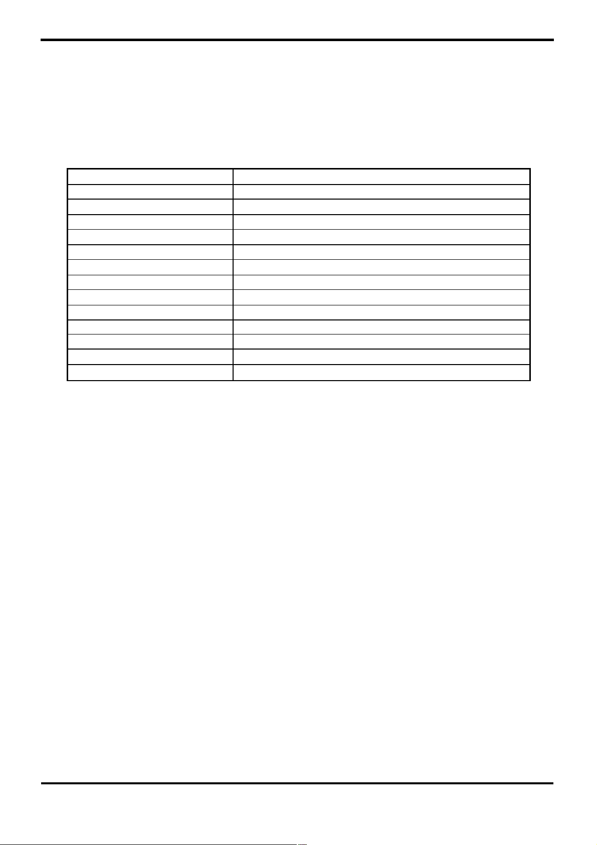
ITEM SPECIFICATION
Display Area(mm) 409.8(H)x230.4(V)
Number of Pixels 1366(H)x768(V)
Pixel Pitch(mm) 0.3(H)x0.3 (V)
Color Pixel Arrangement RGB vertical stripe
Display Mode normally white, TN
Number of Colors 16.7M(6 Bit+Hi-FRC)
Brightness(cd/m^2) 250cd/m2 (Typ.)(center, 60mA)
Viewing Angle(H/V) 170/160 (Typ.)
Surface Treatment Anti-glare, 3H
Power consumption(W)
Module Size(mm) 430.37(W)x254.6(H)x9.9(D)
Module Weight(g)
Backlight Unit LED (White-LED)
(12.5)W(typ)(Without Converter)
1350(typ)
CPT Confidential 2/22
CPT CHUNGHWA PICTURES TUBES, LTD.,
CLAA
215FA04_V4
-Tatung
-
SPEC
-
Tentative
-20101117
0
20
80
2. ABSOLUTE MAXIMUM RATINGS
ITEM SYMBOL
Power Supply Voltage for
LCD
Lightbar Input V
Lightbar Current I
static electricity
Operation Temperature Top 0 50 ℃ 4). 5). 6). 8)
Storage Temperature Tstg -20 60 ℃ 4). 5). 6). 8)
[Note]
1).Product life-time relate to LED, please operate production follow statement at page 8
〝(2)back light〞.
2).When LED current over the definition of operating current(60mA) ,product life-time will
decay rapidly or operate unusual.
3).LED current ripple peak-to-peak must be less then 1.5mA.
4).The relative temperature and humidity range are as below sketch, 90%RHMax.
(Ta40). ≦℃
VCC 0 6 V
LED
57 63 mA
LED
VESDt -200 200 V
VESDc -8000 8000 V
MIN. MAX. UNIT REMARK
(31.9) (39.6)
V
2). 3).
7)
5).The maximum wet bulb temperature ≦39℃(Ta>40℃) and without dewing.
6).If you use the product in an environment which over the definition of temperature and
humidity too long to effect the result of eye-etching.
7) Test Condition: IEC 1000-4-2 VESDt: Contact discharge to input connector; VESDC:
Contact discharge to module
8). If you operate the product in normal temperature range, the center surface of panel
should be under 60 .℃
Relative humidity(%RH)
Operating Range
Storage Range
60
50
-20
20
40
Temperature (°C)
CPT Confidential 3/22
CPT CHUNGHWA PICTURES TUBES, LTD.,
CLAA
215FA04_V4
-Tatung
-
SPEC
-
Tentative
-20101117
Ta=25 ℃
Common Mode
Logic input
t2 t3
0.5V
t4
t6
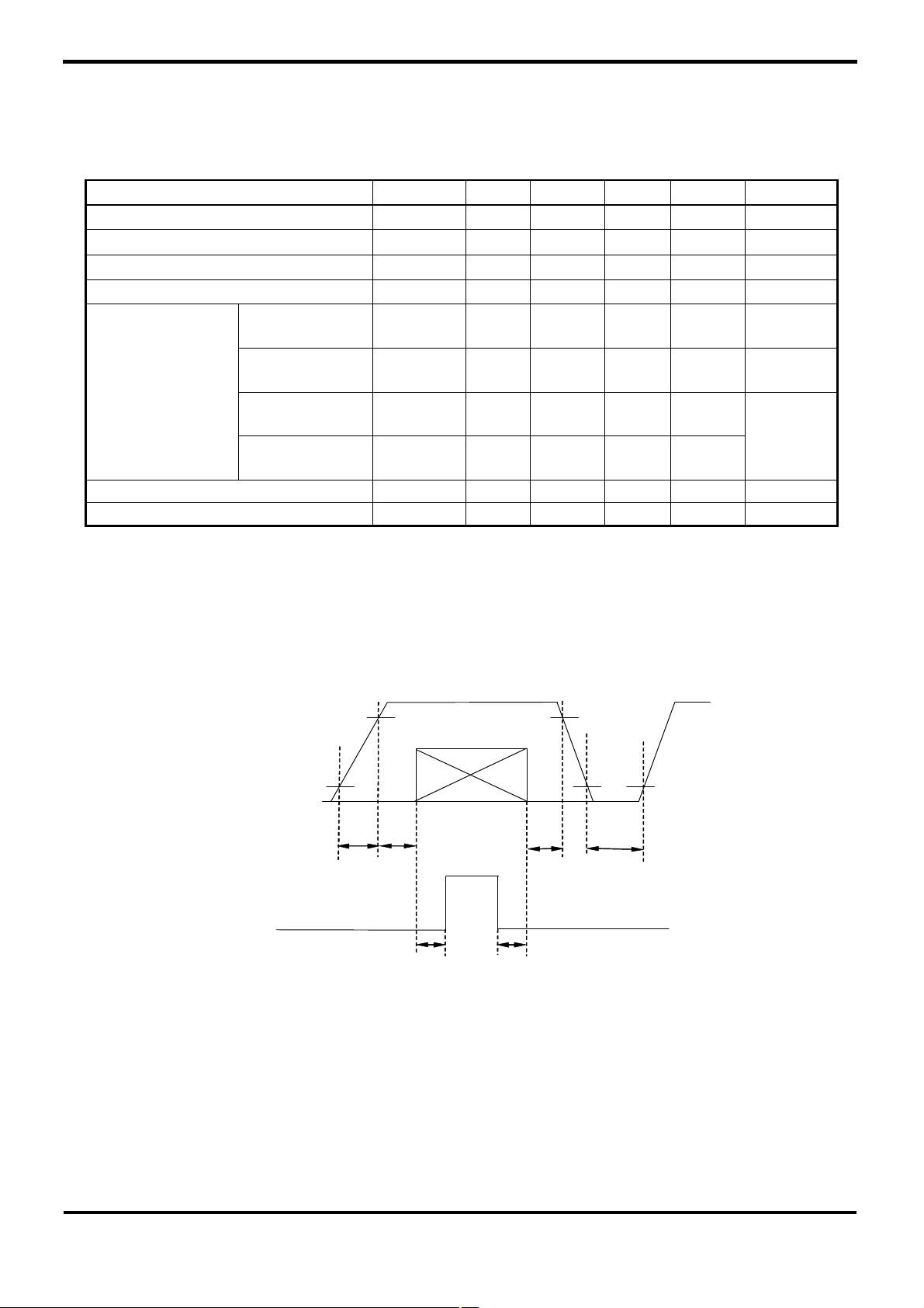
3. ELECTRICAL CHARACTERISTICS
(1).TFT-LCD
ITEM SYMBOL MIN TYP MAX UNIT Remark
Power Supply Voltage for LCD Vcc 4.5 5.0 5.5 V *1)
Power Supply Current for LCD Icc - 700 1000
Permissive Input Ripple Voltage VRP - - 100 mVp-p Vcc=5.0V
Differential impedance Zm 90 100 110 Ω
mA *2)
voltage
LVDS:IN+,IN-
Voltag
Differential
Input Voltage
Threshold
Voltage(High)
Threshold
Voltage(Low)
VCM 1.125 1.25 1.375
|VID| 200 350 600 mV
VTH - - 100 mV
VTL -100
- - mV
V
LCD Inrush Current Inrush 3 A *4)
Power consumption P 3.5 5.5 W *2)
[Note]
1).VCC-turn-on conditions:
0.5mst110ms ≦≦ 1000ms t4≦
0<t250ms 500mst5≦≦
0.5<t350ms 200mst6 ≦≦
4.5V
LCD Power Supply
Logic Signal
0.5V
Vin=5.0V
4.5V
data
0.5V
*3)
t1
Backlight Power Supply
Data: RGB DATA, DCLK, DENA
CPT Confidential 4/22
VL
t5

CPT CHUNGHWA PICTURES TUBES, LTD.,
CLAA
215FA04_V4
-Tatung
-
SPEC
-
Tentative
-20101117
VIN
= Positive differential DATA & CLK Input
VIN
-
= Negative differential DATA & CLK Input
VCC-dip conditions:
(1) When 3.6VVcc(min)<4.5V: td10 ms≦≦
(2) When Vcc <3.6 V, VCC-dip conditions should also follow the VCC-turn-on
conditions.
2).Typical current situation: 256 gray scale level, VCC=5.0V, Fh=47.28KHz, Fv=60Hz,
Fclk=67.1 MHz.
Maxmum current situation: All black pattern, VCC=5.0V, Fh=47.28KHz, Fv=60Hz,
Fclk=67.1 MHz.
3).LVDS Signal definition:
VID = VIN+ – VIN- ,
VCM =△ |VCM+–VCM-|,
VID =△ |VID+–VID-|,
VID+ =|VIH+–VIH-|,
VID- =|VIL+–VIL-|,
+
VCM =(VIN+ +VIN-)/2,
VCM+ =(VIH+ +VIH-)/2,
VCM- =(VIL+ +VIL-)/2,
CPT Confidential 5/22

CPT CHUNGHWA PICTURES TUBES, LTD.,
CLAA
215FA04_V4
-Tatung
-
SPEC
-
Tentative
-20101117
4).Irush Measurement Condition
(2).Backlight
1. Electrical specification
Ta=25℃(Ta:Ambient Temperature)
Symbol
VF
IF LED Operation Current
P
BLU Power -
out
[Note]
1).When LED current over the definition of operating current(60mA) ,product life-time will
decay rapidly or operate unusual
2. life time
ITEM
LIFE TIME
[Note]
Parameter Min.
LED Operation Voltage
(for reference)
Min. Typ. Max. UNIT Note
30000
Typ. Max. Unit Note
-
-
(35.75)
60 (63)
(8.58)
(39.6)
(9.97)
- - hrs
V
mA 1)
W
1),2),3)
CPT Confidential 6/22
1).Parameter guideline for LED driving is under stable conditions at 25 ℃ (Room
Temperature) and IF=60mA
2).Definition of the lamp life time: Luminance (L) under 50% of specification.
3).When the ambient temperature Ta overstep 25℃, it will serious damage life time.
CPT CHUNGHWA PICTURES TUBES, LTD.,
CLAA
215FA04_V4
-Tatung
-
SPEC
-
Tentative
-20101117
L
IGHTBAR
CN2
CN1:
LVDS
BACK of MDL
4. INTERFACE PIN CONNECTION
Pin 1
(1) CN1 (Data Signal and Power Supply)
Interface Connector
Type Part Number
Mating Housing Part
Number
Pin 6
0930G30-B2001A-M4(STARCONN)
MSCKT2407P30H(STM) or compatible
FI-X30HL(JAE) (Locking)
FI-X30H(JAE) (Non-locking)
Pin 1
Pin 30
PIN NO. REMARK FUNCTION
1 NC NC
2 NC NC
3 NC NC
4 GND Power ground
5 RXIN0- Negative LVDS differential data input(0)
6 RXIN0+ Positive LVDS differential data input(0)
7 GND Power ground
8 RXIN1- Negative LVDS differential data input(1)
9 RXIN1+ Positive LVDS differential data input(1)
10 GND Power ground
11 RXIN2- Negative LVDS differential data input(2)
12 RXIN2+ Positive LVDS differential data input(2)
13 GND Power ground
14 RXCLKIN- Negative LVDS differential clock input(clock)
15 RXCLKIN+ Positive LVDS differential clock input(clock)
16 GND Power ground
17 RXIN3- Negative LVDS differential data input(3)
18 RXIN3+ Positive LVDS differential data input(3)
19 GND Power ground
20 NC NC
21 NC NC
22 NC NC
CPT Confidential 7/22
 Loading...