

CPCLA IAD110P, IAD110PTR Datasheet
1
www.clare.com
IAD110P
DS-IAD110P-R2
The IAD110P Multifunction Telecom switch combines a
350V Form A relay and two optocouplers in a single package. The relay uses optically coupled MOSFET technology to provide 1500V of input to output isolation. The
efficient MOSFET switch and photovoltaic die uses
Clare’s patented OptoMOS architecture. The optically
coupled input uses highly efficient GaAIAs infrared LEDs.
IAD110P’s allow telecom circuit designers to combine
three discrete functions in a single component. The
IAD110P’s small package uses less space than traditional discrete component solutions.
• Telecommunications
• Telecom Switching
• Tip/Ring Circuits
• Modem Switching (Laptop, Notebook, Pocket Size)
• Hookswitch
• Dial Pulsing
• Ground Start
• Ringer Injection
• Instrumentation
• Multiplexers
• Data Acquisition
• Electronic Switching
• I/O Subsystems
• Meters (Watt-Hour, Water, Gas)
• Medical Equipment-Patient/Equipment Isolation
• Security
• Aerospace
• Industrial Controls
• UL Recognized: File Number E76270
• CSA Certified: File Number LR 43639-12
• VDE Compatible
• BSI Certified:
• BS EN 60950:1992 (BS7002:1992)
Certificate #:7969
• BS EN 41003:1993
Certificate #:7969
• Three Functions in One Package
• Small 16 Pin SOIC Package (PCMCIA Compatible)
• Bi-Directional Current Sensing
• Bi-Directional Current Switching
• Replaces up to Three or Four Components
• 3750V
RMS
Input/Output Isolation
• FCC Compatible
• No EMI/RFI Generation
• Machine Insertable, Wave Solderable
• Tape & Reel Versions Available
Applications
Features
Description
Approvals
Integrated Telecom Circuits
Ordering Information
Part # Description
IAD110P 16 Pin SOIC (50/Tube)
IAD110PR 16 Pin SOIC (1000/Reel)
IAD110P Units
Load Voltage 350 V
Load Current 100 mA
Max R
ON
35 Ω
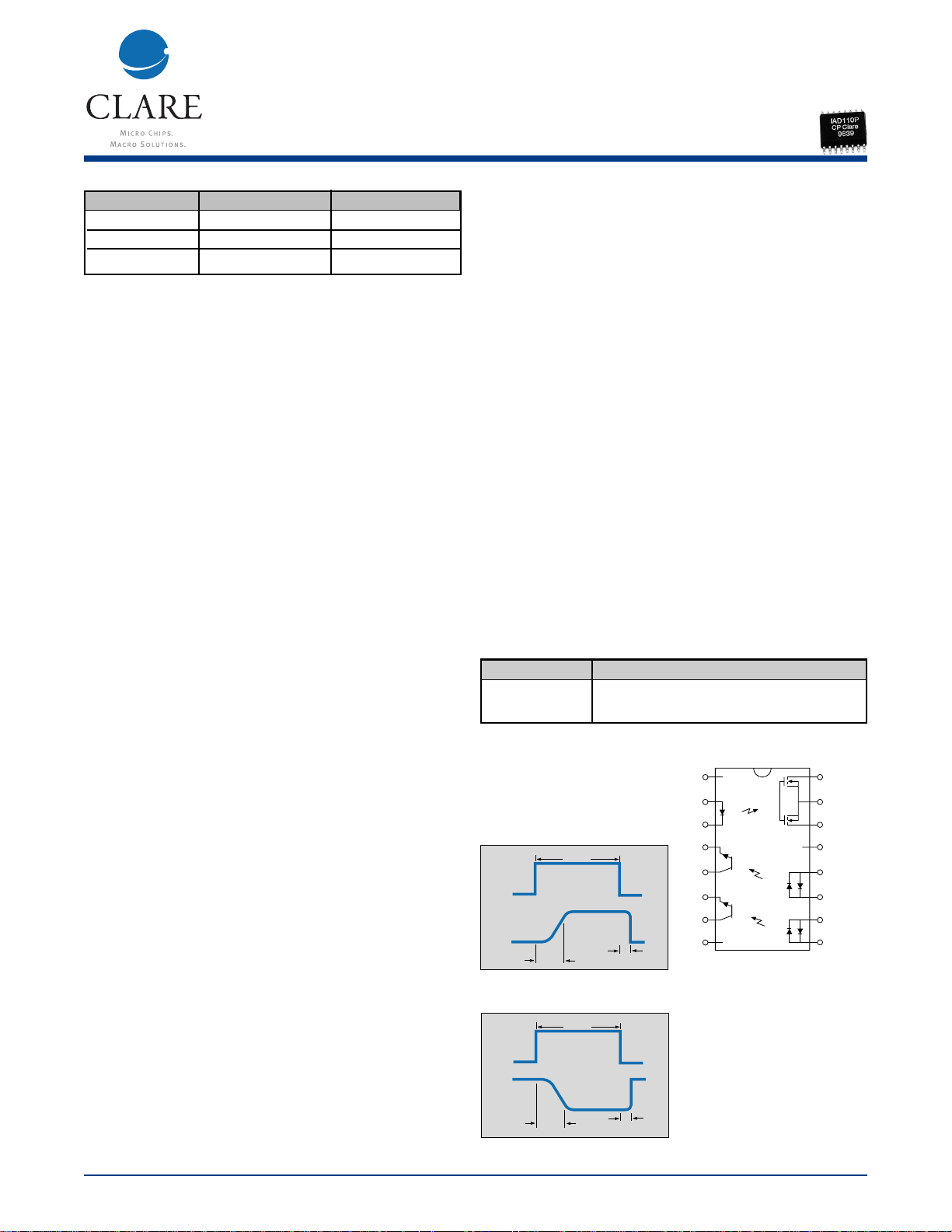
Pin Configuration
IAD110 Pinout
Switching Characteristics of
Normally Open (Form A) Devices
10ms
CONTROL
+
90%
10%
LOAD
Switching Characteristics of
Normally Closed (Form B) Devices
CONTROL
+
T
ON
10ms
90%
+
10%
+
T
OFF
+
10%
T
OFF
+
90%
1
(N/C)
2
3
4
5
6
7
8
(N/C)
1. (N/C)
2. + LED - Relay Input
3. – LED - Relay Input
4. Emitter - Phototransistor #1
5. Collector - Phototransistor #1
6. Emitter - Phototransistor #2
7. Collector - Phototransistor #2
8. (N/C)
9. LED - Phototransistor +/– #2
10. LED - Phototransistor –/+ #2
11. LED - Phototransistor +/– #1
T
ON
12. LED - Phototransistor –/+ #1
13. (N/C)
14. Output - Relay
15. Common - Relay
16. Output - Relay
16
15
(Form A)
14
13
(N/C)
12
11
10
9

www.clare.com
IAD110P
Rev. 2
Absolute Maximum Ratings are stress ratings. Stresses
in excess of these ratings can cause permanent damage
to the device. Functional operation of the device at these
or any other conditions beyond those indicated in the
operational sections of this data sheet is not implied.
Exposure of the device to the absolute maximum ratings
for an extended period may degrade the device and effect
its reliability.
Absolute Maximum Ratings (@ 25˚ C)
2
Parameter Min Typ Max Units
Total Package Dissipation - - 1
1
W
Isolation Voltage
Input to Output 3750 - - V
RMS
Operational Temperature -40 - +85 °C
Storage Temperature -40 - +125 °C
Soldering Temperature - - +220 °C
(10 Seconds Max.)
1
Above 25˚ derate linerity 1.67mw/˚C
Electrical Characteristics
Parameter Conditions Symbol Min Typ Max Units
Relay Portion
Output Characteristics @ 25°C
Load Voltage (Peak) I
L
= 1µA V
L
- - 350 V
Load Current (Continuous) - I
L
- - 100 mA
Peak Load Current 10ms I
LPK
- - 350 mA
On-Resistance I
L
=100mA R
ON
-- 35Ω
Off-State Leakage Current V
L
=350V; TJ=25°C I
LEAK
-- 1µA
Switching Speeds
Turn-On I
F
=5mA, VL=10V T
ON
-- 3ms
Turn-Off I
F
=5mA, VL=10V T
OFF
-- 3ms
Output Capacitance VL=50V, f=1MHz - - 25 - pF
Relay Portion
Input Characteristics @ 25°C
Input Control Current I
L
=100mA I
F
5- 50mA
Input Dropout Current I
L
=1mA I
F
0.4 - - mA
Input Voltage Drop I
F
=5mA V
F
0.9 1.2 1.4 V
Reverse Input Voltage - V
R
-- 5 V
Reverse Input Current VR=5V I
R
- - 10 µA
Detector Portion
Output Characteristics @ 25°C
Phototransistor Blocking Voltage I
C
=10µA BV
CEO
20 50 - V
Phototransistor Dark Current VCE=5V, I
F
=0mA I
CEO
- 50 500 nA
Saturation Voltage I
C
=2mA, IF=16mA V
SAT
- 0.3 0.5 V
Current Transfer Ratio IF=6mA, VCE=0.5V C
TR
33 - - %
Detector Portion
Input Characteristics @ 25°C
Input Control Current I
C
=2mA,VCE=0.5V I
F
62 - mA
Input Voltage Drop IF=5mA I
CEO
0.9 1.2 1.4 V
Input Current I
C
=1µA, VCE=5V - 5 25 - µA
(Detector must be off)
Input to Output Capacitance V
L
=50V, f=1MHz C
I/O
-3 - pF
Input to Output Isolation - V
I/O
3750 - - V
RMS
 Loading...