

CPCLA CPC7582BB-TR, CPC7582BB, CPC7582BA-TR, CPC7582BA Datasheet
Part # Description
CPC7582BA 6 Pole with protection SCR
CPC7582BB 6 Pole without protection SCR
CPC7582BA-TR Tape & Reel Version
CPC7582BB-TR Tape & Reel Version
www.clare.com
DS-CPC7582-R1.0
CPC7582
Line Card Access Switch
1
Applications
Features
Description
Ordering Information
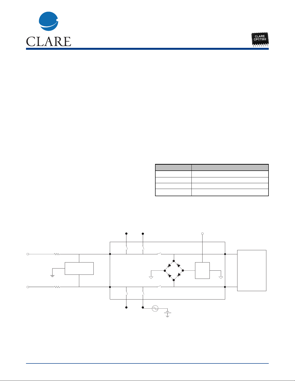
The CPC7582 is a monolithic solid state switch in a 16
pin surface mount SOIC package. It provides the necessary functions to replace two 2-Form-C electromechanical relays on analog line cards found in
Central Office, Access and PBX equipment. The
device contains solid state switches for tip and ring line
break, ring injection/ring return and line test access.
The CPC7582 requires only a +5V supply and offers
“break-before-make” or “make-before-break” switch
operation using simple logic level input control. There
are two versions of the CPC7582, the CPC7582BA
and the CPC7582BB. The “BA” version has a protection SCR which provides protection to the SLIC device
and subsequent circuitry during fault conditions.
• Central office (CO)
• Digital Loop Carrier (DLC)
• PBX Systems
• Digitally Added Main Line (DAML)
• Hybrid Fiber Coax (HFC)
• Fiber in the Loop (FITL)
• Pair Gain System
• Channel Banks
• Small 16 pin surface mount SOIC package
• Monolithic IC reliability
• Low matched RDS
ON
• Eliminates the need for zero cross switching
• Flexible switch timing to transition from ringing mode
to idle/talk mode.
• Clean, bounce free switching
• Tertiary protection consisting of integrated current
limiting, thermal shutdown and SLIC protection
• 5V operation with power consumption <10mW
• Intelligent battery monitor
• Latched logic level inputs, no drive circuitry
• Pin to pin compatible to the Lucent 7582 family
Block Diagram
R1
R2
Ring
TIP
Secondary
Protection
SW1
Break
SW2
Break
SW3
Ringing
Return
SW5
Line Test
Access
SW6
Line Test
Access
SW4
Ringing
Access
SCR
and Trip
Circuit
SLIC
Ring Generator
V
BAT
Reference
CPC7582BA
Battery
+
-
T
ACCESS
(5)
T
RING
(4)
T
LINE
R
LINE
(3)
(14)
R
ACCESS
(12)
R
RING
(13)
R
BAT
(15)
T
BAT
(2)
(16)
Table 1. Break Switch, SW1 and SW2
Parameters Conditions Symbol Min Typ Max Units
Off-state Leakage Current:
+25˚C Vsw (differential)= -320V to Gnd Isw - 0.1 1 µA
Vsw (differential)= -60V to +260V
+85˚C Vsw (differential)= -330V to Gnd Isw - 0.3 1 µA
Vsw (differential)= -60V to +270V
-40˚C Vsw (differential)= -310V to Gnd Isw - 0.1 1 µA
Vsw (differential)= -60V to +250V
RDSON(SW1,SW2):
+25˚C T
LINE
= +/-10 mA, +/-40mA, T
BAT
= -2V ∆ V - 14.5 - Ω
+85˚C T
LINE
= +/-10 mA, +/-40mA, T
BAT
= -2V ∆ V - 20.5 28 Ω
-40˚C T
LINE
= +/-10 mA, +/-40mA, T
BAT
= -2V ∆ V - 10.5 - Ω
RDS
ON
Match Per ON-resistance Test Condition of Magnitude - 0.15 0.8 Ω
SW1, SW2RONSW1-RONSW2
dc Current Limit:
+25˚C Vsw(on) = +/- 10V lsw - 300 - mA
+85˚C Vsw(on) = +/- 10V lsw 80 160 - mA
-40˚C Vsw(on) = +/- 10V lsw - 400 425 mA
Dynamic Current Limit: Break switches in ON state, Ringing Isw - 2.5 - A
(t=<0.5µs) access switches OFF, Apply +/- 1000V
at 10/1000ms pulse, Appropriate
secondary protection in place.
ESD Rating (HBM)
1000V
Power Supply Specifications
Supply Min Typ Max Unit
V
DD
+4.5 +5.0 +5.5 V
V
BAT
1
-19 - -72 V
www.clare.com
2
CPC7582
Rev. 1.0
Absolute Maximum Ratings are stress ratings. Stresses in
excess of these ratings can cause permanent damage to
the device. Functional operation of the device at these or
any other conditions beyond those indicated in the operational sections of this data sheet is not implied. Exposure of
the device to the absolute maximum ratings for an extended period may degrade the device and effect its reliability.
Absolute Maximum Ratings (@ 25˚ C)
Electrical Characteristics TA = -40oC to +85oC
(unless otherwise specified)
Minimum and maximum values are production testing
requirements. Typical values are characteristic of the
device and are the result of engineering evaluations.
Typical values are provided for information purposes
only and are not part of the testing requirements.
1
V
BAT
is used only as a reference for internal protection circuitry.
If V
BAT
rises above -10V, the device will enter an all off state and will remain in the all off state
until the battery voltage drops below -15V.
Parameter Min Max Units
Operating Temperature Range -40 +110 ˚C
Storage Temperature Range -40 +150 ˚C
Relative Humidity Range 5 95 %
Pin Soldering Temperature - +260 ˚C
(t=10 s max)
+5V Power Supply - 7 V
Battery Supply - -85 V
Logic Input Voltage - 7 V
Logic Input to Switch Output Isolation - 330 V
Switch Isolation (SW1, SW2, SW3, SW5, SW6) - 330 V
Switch Isolation
(SW4) -
480 V

CPC7582
www.clare.com
3
Rev. 1.0
Table 1. Break Switch, SW1 and SW2 (Continued)
Parameters Conditions Symbol Min Typ Max Units
Logic Input to Switch Output Isolation:
+25˚C Vsw (T
LINE
, R
LINE
) = +/-320V Isw - 0.1 1 µA
Logic Inputs = Gnd
+85˚C Vsw (T
LINE
, R
LINE
) = +/-330V Isw - 0.3 1 µA
Logic Inputs = Gnd
-40˚C Vsw (T
LINE
, R
LINE
) = +/-310V Isw - 0.1 1 µA
Logic Inputs = Gnd
dv/dt Sensitivity
1
- - - 200 - V/µs
1
Applied voltage is 100 Vp-p square wave at 100Hz.
Table 2. Ring Return Switch, SW3
Parameters Conditions Symbol Min Typ Max Units
Off-state Leakage Current
+25˚C Vsw (differential)= -320V to Gnd Isw - 0.1 1 µA
Vsw (differential)= -60V to +260V
+85˚C Vsw (differential)= -330V to Gnd Isw - 0.3 1 µA
Vsw (differential)= -60V to +270V
-40˚C Vsw (differential)= -310V to Gnd Isw - 0.1 1 µA
Vsw (differential)= -60V to +250V
dc Current Limit:
+25˚C Vsw (on) = +/- 10V Isw - 135 - mA
+85˚C Vsw (on) = +/- 10V Isw - 85 - mA
-40˚C Vsw (on) = +/- 10V Isw - 210 - mA
Dynamic Current Limit: Break switches in ON state, Ringing Isw - 2.5 - A
(t=<0.5ms) access switches OFF, Apply +/- 1000V
at 10/1000ms pulse, Appropriate
secondary protection in place.
RDS
ON
+25˚C Isw (on) = +/-0mA, +/-10mA ∆ V-60-Ω
+85˚C Isw (on) = +/-0mA, +/-10mA ∆ V - 85 100 Ω
-40˚C Isw (on) = +/-0mA, +/-10mA ∆ V-45-Ω
Logic Input to Switch Output Isolation
+25˚C Vsw (T
RING
, T
LINE
) = +/-320V Isw - 0.1 1 µA
Logic Inputs = Gnd
+85˚C Vsw (T
RING
, T
LINE
) = +/-330V Isw - 0.3 1 µA
Logic Inputs = Gnd
-40˚C Vsw (T
RING
, T
LINE
) = +/-310V Isw - 0.1 1 µA
Logic Inputs = Gnd
Table 4. Loop Access Switches, SW5 and SW6
Parameters Conditions Symbol Min Typ Max Units
Off-state Leakage Current
+25˚C Vsw (differential)= -320V to Gnd Isw - 0.1 1 µA
Vsw (differential)= -60V to +260V
+85˚C Vsw (differential)= -330V to Gnd Isw - 0.3 1 µA
Vsw (differential)= -60V to +270V
-40˚C Vsw (differential)= -310 to Gnd Isw - 0.1 1 µA
Vsw (differential)= -60V to +250V
DC Current Limit:
+25˚C Vsw (on) = +/- 10V Isw - 175 - mA
+85˚C Vsw (on) = +/- 10V Isw 80 110 - mA
-40˚C Vsw (on) = +/- 10V Isw - 210 250 mA
Dynamic Current Limit: Break switches in ON state, Ringing Isw - 2.5 - A
(t=<0.5µs) access switches OFF, Apply +/- 1000V
at 10/1000ms pulse, Appropriate
secondary protection in place.
RDSON:
+25˚C Isw (on) = +/-10 mA, +/-40mA ∆ V-38-Ω
+85˚C Isw (on) = +/-10 mA, +/-40mA ∆ V - 46 70 Ω
-40˚C Isw (on) = +/-10 mA, +/-40mA ∆ V-28-Ω
Logic Input to Switch Output Isolation:
+25˚C Vsw (T
ACCESS
, T
LINE
) = +/-320V Isw - 0.1 1 µA
Logic Inputs = Gnd
+85˚C Vsw (T
ACCESS
, T
LINE
) = +/-330V Isw - 0.3 1 µA
Logic Inputs = Gnd
-40˚C Vsw (T
ACCESS
, T
LINE
) = +/-310V Isw - 0.1 1 µA
Logic Inputs = Gnd
Table 3. Ringing Access Switch, SW4
Parameters Conditions Symbol Min Typ Max Units
Off-state Leakage Current
+25˚C Vsw (differential)= -255V to +210V Isw - 0.05 1 µA
Vsw (differential)= +255V to -210V
+85˚C Vsw (differential)= -270V to +210V Isw - 0.1 1 µA
Vsw (differential)= +270V to -210V
-40˚C Vsw (differential)= -245V to +210V Isw - .05 1 µA
Vsw (differential)= +245V to -210V
ON Voltage Isw (on) = +/- 1mA - - 1.5 3 V
Ring Generator Current Vcc = 5V, INaccess = 0 I
R
- 0.1 0.25 mA
During Ring
Surge Current - - - - 2 A
Release Current - - - 300 - µA
RDS
ON
Isw (on) = +/-70mA, +/-80mA ∆ V - 8.5 12 Ω
Logic Input to Switch Output Isolation:
+25˚C Vsw (R
RING
, R
LINE
) = +/-320V Isw - .05 1 µA
Logic Inputs = Gnd
+85˚C Vsw (R
RING
, R
LINE
) = +/-330V Isw - 0.1 1 µA
Logic Inputs = Gnd
-40˚C Vsw (R
RING
, R
LINE
) = +/-310V Isw - .05 1 µA
Logic Inputs = Gnd
www.clare.com
4
CPC7582
Rev. 1.0
 Loading...