

¡
ORDERING INFORMATION
ZUS61205
Output voltage
Input voltage
Output wattage
Single output
Series name
ZUS6
Thin profile
Isolated between input
-
output
Built
-
in overcurrent protection circuit
UL recognized, TÜV approved, CSA certified
Five
-
year warranty
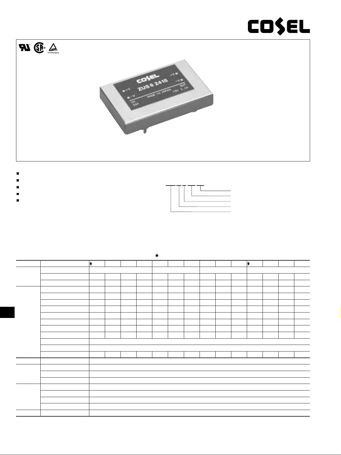
ZU SERIES DC/DC CONVERTER
¶1 Rated input. 5V, 12V, 24V or 48V DC, Io=100%
¶2 The drift is a change at 25ª of ambient temperature and 30 minutes~8 hours after the input voltage applied at rated input/output.
¶3 Measured by 20MHz oscilloscope.
¶ Series/Parallel operation with other model is not possible.
VOLTAGE
CURRENT
EFFICIENCY
VOLTAGE
CURRENT
LINE REGULATION
LOAD REGULATION
RIPPLE ¶3
DRIFT
START-UP TIME
INPUT-OUTPUT
INPUT-CASE
OUTPUT-CASE
VIBRATION
IMPACT
AGENCY APPROVALS
[V]
[A]¶1
[%]¶1
[V]
[A]
[mV]
[mV]
[mVp-p]
[mVp-p]
[mV] ¶2
[ms]
[V]
[V]
STORAGE TEMP.,
HUMID. AND ALTITUDE
OPERATING TEMP.,
HUMID. AND ALTITUDE
OVERCURRENT
PROTECTION
TEMPERATURE
[mV]
REGULATION
-20˚C ~+55˚C
RIPPLE
NOISE
MODEL
ZUS60505
1.41 typ
71 typ
5
1.0
4.85~5.25
ZUS60512
1.63 typ
74 typ
12
0.5
11.40~12.60
ZUS60515
1.63 typ
74 typ
15
0.4
14.25~15.75
0.17 typ
78 typ
15
0.4
14.25~15.75
ZUS61205
0.69 typ
73 typ
5
1.2
4.85~5.25
ZUS61212
DC9~18
0.65 typ
78 typ
12
0.5
11.40~12.60
ZUS61215
0.65 typ
78 typ
15
0.4
14.25~15.75
ZUS62405
0.35 typ
73 typ
5
1.2
4.85~5.25
ZUS62412
DC18~36
0.33 typ
78 typ
12
0.5
11.40~12.60
ZUS62415
0.33 typ
78 typ
15
0.4
14.25~15.75
ZUS64805
0.18 typ
73 typ
5
1.2
4.85~5.25
ZUS64812
0.17 typ
78 typ
12
0.5
11.40~12.60
ZUS64815
DC4.5~9
INPUT
OUTPUT
ISOLATION
SAFETY
PROTECTION
CIRCUIT
ENVIRONMENT
SPECIFICATIONS
Works over 105% of rating and recovers automatically
AC500V, 1 minute. Cutoff current=10mA, DC500V, 50M
Ω min
(At Room Temperature)
AC500V, 1 minute. Cutoff current=10mA, DC500V, 50M
Ω min
(At Room Temperature)
AC500V, 1 minute. Cutoff current=10mA, DC500V, 50M
Ω min
(At Room Temperature)
-20~+71ª, 20~95%RH(Non condensing)(Refer to DERATING CURVE), 3,000m(10,000feet)max
-40~+85ª, 20~95%RH(Non condensing), 9,000m(30,000feet)max
10~55Hz, 98.0m/s
2
(10G), 3 minutes period, 60 minutes along X, Y and Z axis
490.3m/s
2
(50G), 11ms, once each X, Y and Z axis
UL1950, EN60950, CSA C22.2 No.950 Complies with IEC60950
OUTPUT VOLTAGE
SETTING
OUTPUT VOLTAGE
ADJUSTMENT RANGE
20max
40max
80max
120max
50max
20max
ZUS6053R3
0.94 typ
70 typ
3.3
1.0
3.20~3.47
20max
40max
80max
120max
50max
20max
48max
100max
120max
150max
150max
48max
60max
120max
120max
150max
180max
60max
20max
40max
80max
120max
50max
20max
48max
100max
120max
150max
150max
48max
60max
120max
120max
150max
180max
60max
20max
40max
80max
120max
50max
20max
48max
100max
120max
150max
150max
48max
60max
120max
120max
150max
180max
60max
20max
40max
80max
120max
50max
20max
ZUS6483R3
0.09 typ
73 typ
3.3
1.0
3.20~3.47
20max
40max
80max
120max
50max
20max
48max
100max
120max
150max
150max
48max
60max
120max
120max
150max
180max
60max
20max (Minimum input, lo=100%)
FIXED
R
¶3
DC 36~72
marked models are pending for safety approvals. Consult with us for delivery.
392
ZU/ZT
MAX OUTPUT
WATTAGE
DC OUTPUT
VOLTAGE
DC OUTPUT
CURRENT
ZUS6
5V
ZUS6
3.3W
3.3 V
1.0 A
ZUS6
6W
12V
0.5A
ZUS6
6W
15V
0.4A
0505
053R3 483R3
5W
1.0A
1205 2405
6W
1.2A
4805 0512 1212 2412 4812 0515 1215 2415 4815
¡
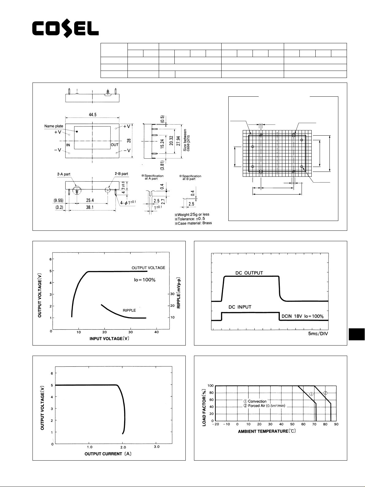
EXTERNAL VIEW
¡
DERATING CURVE
¡
RISE TIME & FALL TIME
(
ZUS62405
)
¡
OVERCURRENT CHARACTERISTICS
(
ZUS62405
)
¡
STATIC CHARACTERISTICS
(
ZUS62405
)
DC/DC CONVERTER
(SINGLE OUTPUT)
Outline
Recomended size for
processing PCB
(TOP VIEW)
15.24
20.32
27.94
(1.25)
(1.25) (1.25)
(1.25)
4-
º
1.5
2-
º
1.6
38.1
25.4
6.35
¶Dimensions in mm
The converter is in contact with the
slanted area of the P.C.B. To keep
isolation, adequate wiring on the
mounted side is required.
¶Div.: 0.1inch
MODEL
393
ZU/ZT
393
Basic characteristics data
Model
310~1600 -
-
-
-
-
-
200~1600
150~1600
100~ 200
330~ 400
330~ 400
*1
Refer to
table No.1
Yes
Yes
Yes
Yes
Yes
Yes
*2
*2
*2
Yes
Yes
Yes
*2
*2
*2
*2
*2
*2
PCB/PatternCircuit
method
Switching
frequency
[kHz]
Series/Parallel
operation availability
*1 Refer to Specification.
*2 Refer to Instruction Manual.
Input
current
[A]
Rated
input fuse
Material Single
sided
Flyback
converter
Flyback
converter
Flyback
converter
Flyback
converter
Single ended
forward converter
Single ended
forward converter
glass fabric base,
epoxy resin
glass fabric base,
epoxy resin
glass fabric base,
epoxy resin
glass fabric base,
epoxy resin
glass fabric base,
epoxy resin
glass fabric base,
epoxy resin
ZUS1R5
ZUW1R5
ZTS1R5
ZTW1R5
ZUS3
ZUW3
ZTS3
ZTW3
ZUS6
ZUW6
ZUS10
ZUW10
ZUS15
ZUW15
ZUS25
ZUW25
Series
operation
Parallel
operation
Double
sided
Inrush
current
protection
Table 1. Rated Input Fuse
Output Power
Input Voltage
5V
1.5W
3 W
6 W
10 W
15 W
25 W
72V
72V
72V
125V
125V
125V
1.2A
2.0A
4.0A
6.3A
8.0A
10.0A
12V
72V
72V
72V
125V
125V
125V
0.8A
1.2A
2.0A
3.5A
5.0A
6.3A
24V
72V
72V
72V
125V
72V
125V
0.8A
0.8A
1.2A
2.0A
2.0A
3.15A
48V
72V
72V
72V
125V
72V
125V
0.8A
0.8A
0.8A
1.0A
2.0A
2.0A
420
ZU/ZT
ZU/ZT
421
Instruction Manual
Pin Connection. . . . . . . . . . . . 422
Function . . . . . . . . . . . . . . . . . . . . 422
2.1 Input voltage . . . . . . . . . . . . . . . . . . . . . . . .422
2.2 Overcurrent protection . . . . . . . . . . . . . . . 422
2.3 Isolation . . . . . . . . . . . . . . . . . . . . . . . . . . . .422
Wiring to Input/Output Pin
. . 423
Series Operation and Parallel Operation
. . 423
4.1 Series operation . . . . . . . . . . . . . . . . . . . . .423
4.2 Parallel redundancy operation . . . . . . . . . 424
Assembling and Installation Method
. . 424
5.1 Installation method . . . . . . . . . . . . . . . . . . 424
5.2 Derating . . . . . . . . . . . . . . . . . . . . . . . . . . . 425
Input Voltage/Current Range
. .425
Cleaning. . . . . . . . . . . . . . . . . . . . .425
Soldering. . . . . . . . . . . . . . . . . . . .425
Input/Output Pin. . . . . . . . . . .426
Peak Current (Pulse Load)
. . 426
10
9
8
7
6
5
4
3
2
1
Pin Connection . . . . . . . . . . . . 427
Function . . . . . . . . . . . . . . . . . . . . 427
2.1 Input voltage . . . . . . . . . . . . . . . . . . . . . . . .427
2.2 Overcurrent protection . . . . . . . . . . . . . . . 427
2.3 Overvoltage protection . . . . . . . . . . . . . . . 427
2.4 Adjustable voltage range . . . . . . . . . . . . . 428
2.5 Remote ON/OFF . . . . . . . . . . . . . . . . . . . .428
2.6 Isolation . . . . . . . . . . . . . . . . . . . . . . . . . . . .428
Wiring to Input/Output Pin
. . 429
Series Operation and Parallel Operation
. . 429
4.1 Series operation . . . . . . . . . . . . . . . . . . . . .429
4.2 Parallel redundancy operation . . . . . . . . . 430
Assembling and Installation Method
. .430
5.1 Installation method . . . . . . . . . . . . . . . . . . .430
5.2 Derating . . . . . . . . . . . . . . . . . . . . . . . . . . . .430
Input Voltage/Current Range
. .431
Cleaning. . . . . . . . . . . . . . . . . . . . .431
Soldering. . . . . . . . . . . . . . . . . . . .431
Input/Output Pin. . . . . . . . . . .432
Peak Current (Pulse Load)
. . 432
10
9
8
7
6
5
4
3
2
1
ZU1R5 • ZU3 • ZU6 • ZU10
Pin Connection . . . . . . . . . . . 433
Function . . . . . . . . . . . . . . . . . . . . 433
2.1 Input voltage . . . . . . . . . . . . . . . . . . . . . . . .433
2.2 Overcurrent protection . . . . . . . . . . . . . . . .433
2.3 Isolation . . . . . . . . . . . . . . . . . . . . . . . . . . . .433
Wiring to Input/Output Pin
. . 434
Series Operation and Parallel Operation
. . 434
4.1 Series operation . . . . . . . . . . . . . . . . . . . . .434
4.2 Parallel redundancy operation . . . . . . . . . 435
Assembling and Installation Method
. . 435
5.1 Installation method . . . . . . . . . . . . . . . . . . 435
5.2 Derating . . . . . . . . . . . . . . . . . . . . . . . . . . . .435
Input Voltage/Current Range
. .435
Cleaning. . . . . . . . . . . . . . . . . . . . .436
Soldering. . . . . . . . . . . . . . . . . . . .436
Input/Output Pin. . . . . . . . . . .436
Peak Current (Pulse Load)
. . 437
10
9
8
7
6
5
4
3
2
1
ZT1R5 • ZT3
ZU15 • ZU25
1. Pin Connection
¿
Single Output
¿
Dual(±)Output
¿
connecting pin
Case connecting pin is available. By connecting this pin to
-side of input, the radiation noise from main body can be
reduced.
2. Function
2.1 Input voltage
¡
If the wrong input is applied, the unit will not operate properly and/or may be damaged.
2.2 Overcurrent protection
¡
Overcurrent protection circuit is built-in and comes into effect at over 105% of the rated current.
Overcurrent protection prevents the unit from short circuit and over current condition of less than 20 sec. The unit automatically recovers
when the fault condition is cleared.
¡
The power supply which has a current foldback characteristics may not start up when connected to nonlinear load such as lamp, motor or
constant current load. See the characteristics below.
Fig. 2.1 Current foldback characteristics
2.3 Isolation
¡
For a receiving inspection, such as Hi-Pot test, gradually increase(decrease)the voltage for the start(shut down). Avoid using Hi-Pot
tester with the timer because it may generate voltage a few times higher than the applied voltage, at ON/OFF of a timer.
422
ZU1R5 • ZU3 • ZU6 • ZU10
ZU/ZT
No.
q
w
e
r
t
Pin connection Function
+DC INPUT
-DC INPUT
+DC OUTPUT
COMMON
-DC OUTPUT
Case connecting
pin
If connected to -side of input, the case potential can be
fixed and the value of radiation noise can be reduced.
+Side of input voltage
-Side of input voltage
+Side of output voltage
GND of output voltage(Only applicable for Dual output)
-Side of output voltage
y
: Load characteristics of power supply
: Characteristics of load (lamp, motor, constant current load, etc.)
Note: In case of nonlinear load, the output is locked out at A point.
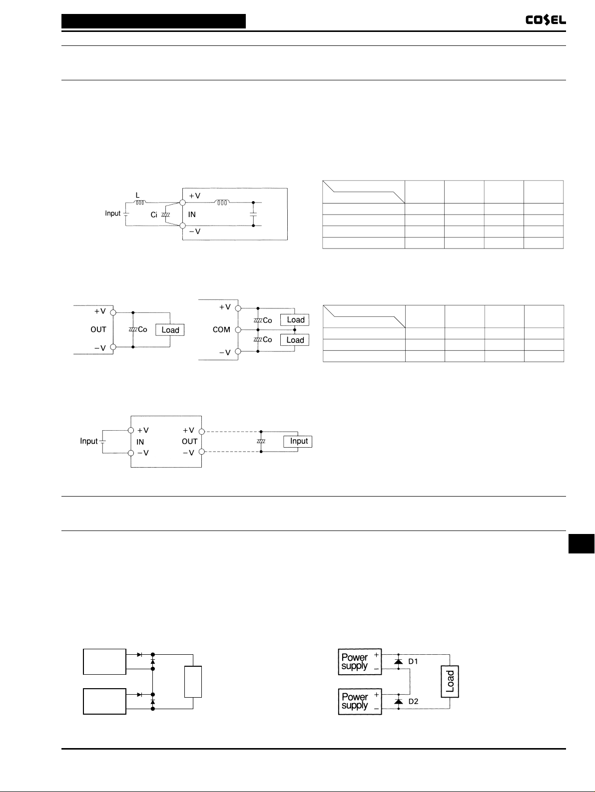
3. Wiring to Input/Output Pin
¡
Input filter is built
-
in. A capacitor Ci, if installed near the input terminal, will lower the input conducted noise from converter due to the
formation of the π type filter.
¡
When the distance from the DC line to the unit is greatly extended, it makes the input feedback noise much higher and the input voltage
several times higher than the normal level when turned ON. If this happens, the output power also becomes unstable. In order to prevent
the unit form failing in this way; please connect Ci to the input terminal. In addition, when the filter with "L" is used, please Ci to the input
terminal.
Capacity of external capacitor at input terminal: Ci[
µ
F]
Fig. 3.1 Connecting method of capacitor at input terminal
¡
To lower the output ripple voltage further, install an external capacitor Co at output terminal as shown below.
Capacity of external capacitor at output terminal: Co[
µ
F]
ZUS ZUW
Fig. 3.2 Connecting method of external capacitor at output terminal
¡
When the distance between load and DC output is long, please install capacitor at load as shown below.
Fig. 3.3 Connection method of capacitor at load
4. Series Operation and Parallel Operation
4.1 Series operation
¿
ZUS1R5/ZUW1R5 • ZUS3/ZUW3 • ZUS6/ZUW6
¡
Series operation is available by connecting the outputs of two or more power supplies, as shown below. Output currents in series
connection should be lower than the lowest rated current in each unit.
But at series operation with same output voltage, diode is not required to attach even if at (a).
When the output voltage is less than 5V. When the output voltage is more than 12V.
D1~D4: Please use Schottky Barrier Diode. D1 · D2: Please use Schottky Barrier Diode.
423
ZU1R5 • ZU3 • ZU6 • ZU10
ZU/ZT
Model ZUSIR5
ZUWIR5
100
47
33
10
ZUS3
ZUW3
220
100
47
22
ZUS6
ZUW6
470
220
100
47
ZUS10
ZUW10
470
220
100
47
5
12
24
48
Input voltage(V)
Model ZUS1R5
ZUW1R5
100
100
100
ZUS3
ZUW3
220
100
100
ZUS6
ZUW6
220
100
100
ZUS10
ZUW10
220
100
100
3, 5
12
15
Output voltage(V)
Power
supply
+
-
Power
supply
+
-
Load
D1
D2
D4
D3

¿
ZUS10/ZUW10
¡
Series operation is available by connecting the outputs of two or more power supplies as shown below. Output currents in series
connection should be lower than the lowest rated current in each unit.
(c) (d)
4.2 Parallel redundancy operation
¡
Parallel redundancy operation is available by connecting the units as shown below.
I
1, I2 the rated current value
5. Assembling and Installation Method
5.1 Installation method
¡
The unit can be mounted in any direction. Position them with proper intervals to allow enough air ventilation. Ambient temperature around
each power supply should not exceed the temperature range shown in derating curve.
¡
Avoid placing the DC input line pattern layout underneath the unit because it will increase the line conducted noise. Make sure to leave an
ample distance between the line pattern layout and the unit. Also, avoid placing the DC output line pattern underneath the unit because it
may increase the output noise. Lay out the pattern away from the unit.
Fig. 5.1 Pattern wiring
424
ZU1R5 • ZU3 • ZU6 • ZU10
ZU/ZT
YES
NO

5.2 Derating
¡
By derating the output current, it is possible to operate the unit from -20ª~+71ª (-20ª~+85ª at forced air cooling).
¡
When unit mounted any way other than in drawings below, it is required to consider ventilated environments by forced air cooling or
temperature/load derating. For details, please consult our sales or engineering department.
6. Input Voltage/Current Range
¡
When a non-regulated source is used as a front end, make sure that the voltage fluctuation together with the ripple voltage will not exceed
the input voltage range.
¡
Select the converter that is able to handle the start
-
up current(Ip).
Fig. 6.1 Input current characteristics
7. Cleaning
¡
Cleaning is possible by below listed conditions.
Cleaning method
¡
During cleaning to drying (the condition that cleaning liquid is soaked into the ink of name plate), do not touch on the surface of name
plate.
¡
After cleaning, dry them enough.
8. Soldering
¡
Flow soldering : 260ª less than 15 seconds.
¡
Soldering iron : 450ª less than 5 seconds.
425
ZU1R5 • ZU3 • ZU6 • ZU10
ZU/ZT
No.
Classification
1
2
3
4
Cleaning agents Cleaning method
Liquid Temp.
Pine Alpha ST–100S(ARAKAWA CHEMICAL CO.)
Clean Through 750H(KAO Corporation)
IPA
Asahiklin AK–225AES(ASAHI GLASS CO.)
Varnishing or Ultra
sonic wave
Less than
60˚C
Period
Within 5
minutes
Within 2
minutes
–
Varnishing,Ultra sonic
wave, Vapor
Water type
Solvent type

9. Input/Output Pin
¡
When too much stress is applied on the input/output pins of the unit, the internal connection may be weakened. As below Fig. 9.1, avoid
applying stress of more than 19.6N(2kgf) on the pins horizontally and more than 39.2N(4kgf) vertically.
¡
The input/output pins are soldered on PCB internally, therefore, do not pull or bend them with abnormal forces.
¡
When additional stress is expected to be put on the input/output pins because of vibration or impacts, fix the unit on PCB (using silicone
rubber or fixing fittings) to reduce the stress onto the input/output pins.
Fig. 9.1 Stress onto the pins
10. Peak Current (Pulse Load)
¡
It is possible to supply the pulse current for the pulse load by connecting the capacitor externally at the output side.
¡
The average current Iav of output is shown in below formula.
¡
The required electrolytic capacitor C is found by below formula.
426
ZU1R5 • ZU3 • ZU6 • ZU10
ZU/ZT
Iav = Is +
(Iop - Is)t
T
C =
(Iop - Iav)t
∆Vo

1. Pin Connection
¿
Single Output
¿
Dual (±) Output
2. Function
2.1 Input voltage
¡
If the wrong input is applied, the unit will not operate properly and/or may be damaged.
2.2 Overcurrent protection
¡
Overcurrent protection circuit is built
-
in and comes into effect at over 105% of the rated current.
Overcurrent protection prevents the unit from short circuit and over current condition of less than 20 sec.
The unit automatically recovers when the fault condition is cleared.
Fig. 2.1 Overcurrent protection characteristics
2.3 Overvoltage protection
Single Output
¡
The overvoltage protection circuit is built-in and comes into effect at 115~140% of the rated voltage. The DC input voltage should be
shut down if overvoltage protection is in operation. The minimum interval of DC recycling for recovery 2 to 3 minutes(*).
* The recovery time depends on input voltage.
Multiple Output
¡
By detecting overvoltage condition between +V and -V, overvoltage protection circuit comes into effect at 115~140% of the rated
voltage.The DC input voltage should be shut down if overvoltage protection is in operation. The minimum interval of DC recycling for
recovery 2 to 3 minutes(*).
* The recovery time depends on input voltage.
Remarks:
Please note that unit's internal components may be damaged if excessive voltage(over rated voltage)is applied to output terminal of
power supply. This could happen when the customer tests the overvoltage performance of the unit.
427
ZU15 • ZU25
ZU/ZT
No.
q
w
e
r
t
y
u
Pin connection Function
+DC INPUT
-DC INPUT
RC
+DC OUTPUT
COMMON
-DC OUTPUT
TRM
+Side of input voltage
-Side of input voltage
Remote ON/OFF
+Side of output voltage
GND of output voltage(Only applicable for Dual output)
-Side of output voltage
Adjustment voltage range

2.4 Adjustable voltage range
¡
The output voltage is adjustable by external potentiometer.
¡
When the output voltage adjustment is not used, open the TRM pin.
¡
The over voltage protection circuit comes into effect when the output voltage is set too high.
¡
Output voltage is increased by turning potentiometer clockwise and is decreased by turning potentiometer counterclockwise.
¡
The wiring to the potentiometer should be as short as possible and connected to the remote sensing pins (+S and -S).
The temperature coefficient varies depending on the type of resistor and potentiometer.
It is recommended that the following types be used.
Resistor .............. Metal film type. coefficient of less than ±300ppm/ª
Potentiometer........ Cermet type, coefficient of less than ±100ppm/ª
Fig. 2.2 Connection devices outside the power supply
Table 2.1 Devices outside the power supply (Adjustable ±5%)
2.5 Remote ON/OFF
¡
The ground terminal of remote ON/OFF circuit is connected with -V input terminal.
Between RC and -V input: Output voltage is ON at “Low” level or short circuit(0~1.2V)
Between RC and -V input: Output voltage is OFF at “High” level or open circuit(2.4~5.5V)
(Connection example)
or or
Transistor IC Relay
When RC terminal is “Low” level, fan out current is 1mA typ. When Vcc is applied, use 5V
Vcc 24V. When remote ON/OFF function
is not used, please short between RC and -V input.
2.6 Isolation
¡
For a receiving inspection, such as Hi-Pot test, gradually increase(decrease)the voltage for the start(shut down). Avoid using Hi-Pot
tester with the timer because it may generate voltage a few times higher than the applied voltage, at ON/OFF of a timer.
428
ZU15 • ZU25
ZU/ZT
No.
Output
voltage
1
2
3
4
5
3.3V
5V
12V
±12V
±15V
VR
1K
1K
5K
5K
5K
R1
470
100
270
10K
10K
The constant value of devices outside the power supply
(Unit: Ω)
R2
150
270
2.7K
3.9K
2.7K

3. Wiring to Input/Output Pin
¡
The input filter is built
-
in. A capacitor(Ci),if installed near the input terminal, will lower the input conducted noise from converter due to the
formation of the π type filter.
¡
When the distance from the DC line to the unit is greatly extended, it makes the input feedback noise much higher and the input voltage
several times higher than the normal level when turned ON. If this happens, the output power also becomes unstable. In order to prevent
the unit form failing in this way; please connect Ci to the input terminal. In addition, when the filter with "L" is used, please connect Ci to the
input terminal.
Capacity of external capacitor at input terminal: Ci[
µ
F]
Fig. 3.1 Connection method of capacitor at input terminal
¡
To decrease the ripple voltage further, install an external capacitor Co at output terminal as shown below.
Capacity of external capacitor at output terminal: Co[
µ
F]
ZUS ZUW
Fig. 3.2 Connecting method of external capacitor at output terminal
¡
When the distance between load and DC output is long, please install capacitor at load as below.
Fig. 3.3 Connection method of capacitor at load
4. Series Operation and Parallel Operation
4.1 Series operation
¡
Series operation is available by connecting the outputs of two or more power supplies, as shown below.
Output currents in series connection should be lower than the lowest rated current in each unit.
(a) (b)
429
ZU15 • ZU25
ZU/ZT
Model ZUS15
ZUW15
ZUS25
ZUW25
330
150
68
33
470
220
100
47
5
12
24
48
Input voltage(V)
Model ZUS15
ZUW15
ZUS25
ZUW25
220
100
100
220
100
100
3, 5
12
15
Output voltage(V)

4.2 Parallel redundancy operation
¡
Parallel redundancy operation is available by connecting the units as shown below.
¡
Values of I
1 and I2 become unbalanced by a slight different of the output voltage. Make sure that the output voltage of units is of equal
value and the output current from each power supply does not exceed the rated current.
I
1, I2
the rated current value
¡
Use external potentiometer is recommended which can adjust the output voltage.
5. Assembling and Installation Method
5.1 Installation method
¡
The unit can be mounted in any direction. Position them with proper intervals to allow enough air ventilation. Ambient temperature around
each power supply should not exceed the temperature range shown in derating curve.
¡
Avoid placing the DC input line pattern layout underneath the unit because it will increase the line conducted noise. Make sure to leave an
ample distance between the line pattern layout and the unit. Also, avoid placing the DC output line pattern underneath the unit because it
may increase the output noise. Lay out the pattern away from the unit.
Fig. 5.1 Pattern wiring
5.2 Derating
¡
By derating the output current, it is possible to operate the unit from -20ª~+71ª (-20ª~+85ª at forced air cooling).
¡
When unit mounted any way other than in drawings below, it is required to consider ventilated environments by forced air cooling or
temperature/load derating. For details, please consult our sales or engineering departments.
Fig. 5.2 Derating curve
430
ZU15 • ZU25
ZU/ZT
YES
NO

¡
The temperature increase of case surface at full load is shown by below table as referenced data.
Temperature increase on surface of case (ZU series) (Unit: deg)
6. Input Voltage/Current Range
¡
When a non-regulated source is used as a front end, make sure that the voltage fluctuation together with the ripple voltage will not exceed
the input voltage range.
¡
Select the converter that is able to handle the start-up current(Ip).
Fig. 6.1 Input current characteristics
7. Cleaning
¡
Cleaning agents :
¡
Cleaning period : The total time of varnishing, ultrasonic wave and vaper should be within 2 minutes. In case of ultrasonic wave cleaning,
the ultrasonic should be less than 15kw/m
3
. During cleaning to drying (the condition that cleaning liquid is soaked into
the ink of name plate), do not touch on the surface of name plate.
¡
After cleaning, dry them enough.
8. Soldering
¡
Flow soldering : 260ª less than 15 seconds.
¡
Soldering iron : 450ª less than 5 seconds.
431
ZU15 • ZU25
ZU/ZT
Input Voltage Output Voltage
3V, 5V
12V
±12V
±15V
5V
12V
±12V
±15V
5V
12V
±12V
±15V
3V, 5V
12V
±12V
±15V
30
36
39
38
28
34
36
35
31
38
34
27
21
23
24
26
38
42
39
40
36
42
43
45
32
38
36
35
28
25
31
31
15W 25W
5V
12V
24V
48V
No.
Classification
Cleanig agents
1
2
3
4
Pine Alpha ST-100S(ARAKAWA CHEMICAL CO.)
Clean Through 750H(KAO Corporation)
IPA
Asahiklin AK-225AES(ASAHI GLASS CO.)
Water type
Solvent type

9. Input/Output Pin
¡
When too much stress is applied on the input/output pins of the unit, the internal connection may be weakened. As below Fig. 9.1, avoid
applying stress of more than 19.6N(2kgf)on the pins horizontally and more than 39.2N(4kgf)vertically.
¡
The input/output pins are soldered on PCB internally, therefore, do not pull or bend them with abnormal forces.
¡
When additional stress is expected to be put on the input/output pins because of vibration or impacts, fix the unit on PCB (using silicone
rubber or fixing fittings) to reduce the stress onto the input/output pins.
Fig. 9.1 Stress onto the pins
10. Peak Current (Pulse Load)
¡
It is possible to supply the pulse current for the pulse load by connecting the capacitor externally at the output side.
¡
The average current Iav of output is shown in below formula.
¡
The required electrolytic capacitor C is found by below formula.
432
ZU15 • ZU25
ZU/ZT
Iav = Is +
(Iop - Is)t
T
C =
(Iop - Iav)t
∆Vo

433
ZU/ZT
1. Pin Connection
¿
Single Output
¿
Dual(±)Output
¿
Case Connectiong Pin
Case connecting pin is available. By connecting the pin to -side
of input, the radiation noise from main body can be reduced.
2. Function
2.1 Input voltage
¡
If the wrong input is applied, the unit will not operate properly and/or may be damaged.
2.2 Overcurrent protection
¡
Overcurrent protection circuit is built-in and comes into effect at over 105% of the rated current.
Overcurrent protection prevents the unit from short circuit and over current condition of less than 20 sec. The unit automatically recovers
when the fault condition is cleared.
¡
The power supply which has a current foldback characteristics may not start up when connected to nonlinear load such as lamp, motor or
constant current load. See the characteristics below.
Fig. 2.1 Current foldback characteristics
2.3 Isolation
¡
For a receiving inspection, such as Hi-Pot test, gradually increase(decrease)the voltage for the start(shut down). Avoid using Hi-Pot
tester with the timer because it may generate voltage a few times higher than the applied voltage, at ON/OFF of a timer.
ZT1R5 • ZT3
q-Vw
+V
r+Vt
NC
COM
y
-V
e
S
IN OUT
No.
q
w
e
r
t
y
Pin connection Function
-DC INPUT
+DC INPUT
+DC OUTPUT
NC(Single output)
COM(Dual output)
-DC OUTPUT
If connected to -side of input, the case potential can be
fixed and the value of radiation noise can be reduced.
-Side of input voltage
+Side of input voltage
+Side of output voltage
No Connection
GND of output voltage(Only applicable for Dual output)
-Side of output voltage
Case Connecting
Pin
: Load characteristics of power supply
: Characteristics of load (lamp, motor, constant current load, etc.)
Note: In case of nonlinear load, the output is locked out at A point.

434
3. Wiring to Input/Output Pin
¡
Input filter is built
-
in. A capacitor Ci, if installed near the input terminal, will lower the input conducted noise from converter due to the
formation of the π type filter.
¡
When the distance from the DC line to the unit is greatly extended, it makes the input feedback noise much higher and the input voltage
several times higher than the normal level when turned ON. If this happens, the output power also becomes unstable. In order to prevent
the unit form failing in this way; please connect Ci to the input terminal. In addition, when the filter with "L" is used, please Ci to the input
terminal.
Capacity of external capacitor at input terminal: Ci[
µ
F]
Fig. 3.1 Connecting method of capacitor at input terminal
¡
To lower the output ripple voltage further, install an external capacitor Co at output terminal as shown below.
Capacity of external capacitor at output terminal: Co[
µ
F]
ZTS ZTW
Fig. 3.2 Connecting method of external capacitor at output terminal
¡
When the distance between load and DC output is long, please install capacitor at load as shown below.
Fig. 3.3 Connection method of capacitor at load
4. Series Operation and Parallel Operation
4.1 Series operation
¡
Series operation is available by connecting the outputs of two or more power supplies, as shown below. Output currents in series
connection should be lower than the lowest rated current in each unit.
But at series operation with same output voltage, diode is not required to attach even if at (a).
When the output voltage is less than 5V. When the output voltage is more than 12V.
D1~D4: Please use Schottky Barrier Diode. D1, D2: Please use Schottky Barrier Diode.
ZU/ZT
ZT1R5 • ZT3
Model ZTSIR5
ZTWIR5
100
47
33
10
ZTS3
ZTW3
220
100
47
22
5
12
24
48
Input voltage(V)
Model ZTS1R5
ZTW1R5
100
100
100
ZTS3
ZTW3
220
100
100
5
12
15
Output voltage(V)
Power
supply
+
-
Power
supply
+
-
Load
D1
D2
D4
D3

435
4.2 Parallel redundancy operation
¡
Parallel redundancy operation is available by connecting the units as shown below.
I
1, I2
the rated current value
5. Assembling and Installation Method
5.1 Installation method
¡
The unit can be mounted in any direction. Install the device, with proper intervals to allow enough air ventilation.
5.2 Derating
¡
Ambient temperature around each power supply should not exceed
the temperature range shown in derating curve.
6. Input Voltage/Current Range
¡
When a non-regulated source is used as a front end, make sure that the voltage fluctuation together with the ripple voltage will not exceed
the input voltage range.
¡
Select the converter that is able to handle the start-up current(Ip).
Fig. 6.1 Input current characteristics
ZU/ZT
ZT1R5 • ZT3
100
50
13
4
0
-
20 0 102030405060
(71) (85)
70 80 90
-
10
Load factor [%]
Ambient temperature [ª]
¶1 ZTS30512, ZTS30515
ZTW30512, ZTW30515
1
Convection[¶1 models]
2
Convection[Other models]
3
Forced air(500R/min)[¶1 models]
4
Forced air(500R/min)[Other models]
2

436
7. Cleaning
¡
Cleaning is possible by below listed conditions.
Cleaning method
¡
During cleaning to drying (the condition that cleaning liquid is soaked into the ink of name plate), do not touch on the surface of name
plate.
¡
After cleaning, dry them enough.
8. Soldering
¡
Flow soldering : 260ª less than 15 seconds.
¡
Soldering iron : 450ª less than 5 seconds.
9. Input/Output Pin
¡
When too much stress is applied on the input/output pins of the unit, the internal connection may be weakened. As below Fig. 9.1, avoid
applying stress of more than 9.8N(1kgf) on the pins horizontally and more than 19.6N(2kgf) vertically.
¡
When additional stress is expected to be put on the input/output pins because of vibration or impacts, fix the unit on PCB (using silicone
rubber or fixing fittings) to reduce the stress onto the input/output pins.
Fig. 9.1 Stress onto the pins
ZU/ZT
ZT1R5 • ZT3
No.
Classification
1
2
3
4
Cleaning agents Cleaning method
Liquid Temp.
Pine Alpha ST–100S(ARAKAWA CHEMICAL CO.)
Clean Through 750H(KAO Corporation)
IPA
Asahiklin AK–225AES(ASAHI GLASS CO.)
Varnishing or Ultra
sonic wave
Less than
60˚C
Period
Within 5
minutes
Within 2
minutes
–
Varnishing,Ultra sonic
wave, Vapor
Water type
Solvent type
Less than
9.8N(1kgf)
Less than
9.8N(1kgf)
Less than 19.6N(2kgf)
A part
A

437
10. Peak Current (Pulse Load)
¡
It is possible to supply the pulse current for the pulse load by connecting the capacitor externally at the output side.
¡
The average current Iav of output is shown in below formula.
¡
The required electrolytic capacitor C is found by below formula.
ZU/ZT
ZT1R5 • ZT3
Iav = Is +
(Iop - Is)t
T
C =
(Iop - Iav)t
∆Vo
 Loading...