

Page 1
On-board type
Instruction Manual
ZU1R5 ZU3 ZU6 10ZU
Pin Connection
1
2
Function
Input voltage
2.1
Overcurrent protection
2.2
Isolation
2.3
3
Wiring to Input/Output Pin
Series Operation and Parallel Operation
4
Series operation
4.1
Parallel redundancy operation
4.2
5
Assembling and Installation Method
Installation method
5.1
Derating
5.2
6
Input Voltage/Current Range
7
Cleaning
8
Soldering
9
Input/Output Pin
10
Peak Current (Pulse Load)
F-94
F-94
F-94
F-94
F-94
F-94
F-95
F-95
F-96
F-96
F-96
F-96
F-97
F-97
F-97
F-97
F-97
ZT1R5 ZT3
Pin Connection
1
2
Function
Input voltage
2.1
Overcurrent protection
2.2
Isolation
2.3
3
Wiring to Input/Output Pin
Series Operation and Parallel Operation
4
Series operation
4.1
Parallel redundancy operation
4.2
5
Assembling and Installation Method
Installation method
5.1
Derating
5.2
6
Input Voltage/Current Range
7
Cleaning
8
Soldering
9
Input/Output Pin
10
Peak Current (Pulse Load)
F-103
F-103
F-103
F-104
F-104
F-104
F-105
F-105
F-105
F-105
F-105
F-105
F-105
F-106
F-106
F-106
F-106
ZU15 ZU25
Pin Connection
1
2
Function
Input voltage
2.1
Overcurrent protection
2.2
Overvoltage protection
2.3
Adjustable voltage range
2.4
Remote ON/OFF
2.5
Isolation
2.6
3
Wiring to Input/Output Pin
Series Operation and Parallel Operation
4
Series operation
4.1
Parallel redundancy operation
4.2
5
Assembling and Installation Method
Installation method
5.1
Derating
5.2
6
Input Voltage/Current Range
7
Cleaning
8
Soldering
F-98
F-98
F-98
F-98
F-99
F-99
F-99
F-99
F-100
F-100
F-100
F-100
F-101
F-101
F-101
F-102
F-102
F-102
ZU/ZT
9
Input/Output Pin
10
Peak Current (Pulse Load)
F-102
F-103
F-93
Page 2
On-board type
ZU1R5 ZU3 ZU6 ZU10
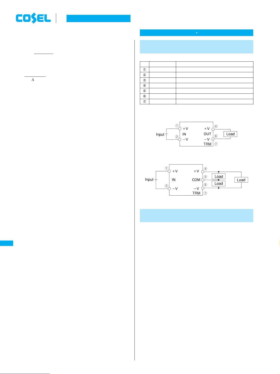
1 Pin Connection
No. Pin connection Function
+DC INPUT
-DC INPUT
+DC OUTPUT
COMMON
-DC OUTPUT
Case connecting
pin
+Side of input voltage
-Side of input voltage
+Side of output voltage
GND of output voltage (Only applicable for Dual output)
-Side of output voltage
If connected to -side of input, the case potential can be
fixed and the value of radiation noise can be reduced.
Instruction anualM
nThe power supply which has a current foldback characteristics
may not start up when connected to nonlinear load such as lamp,
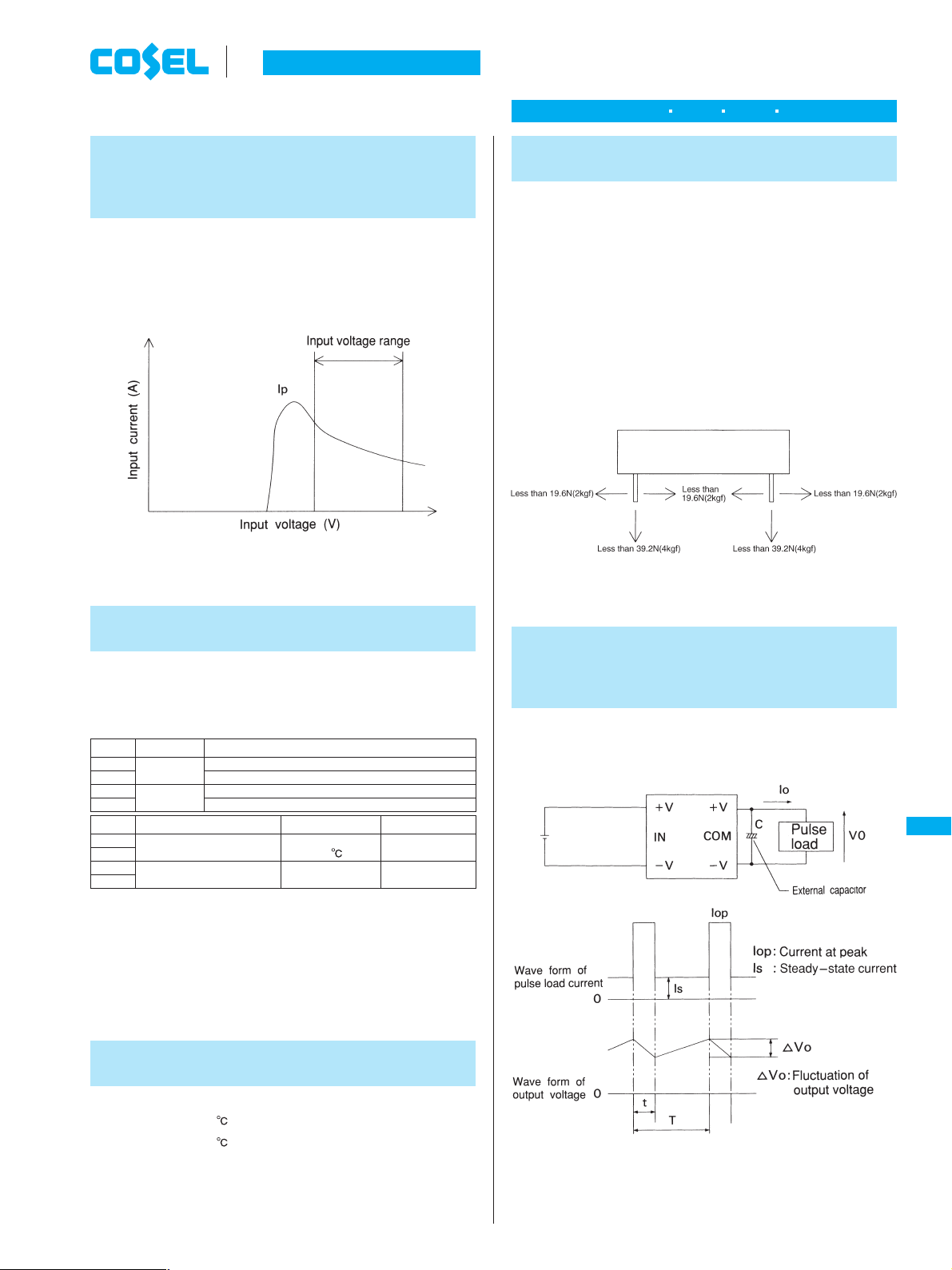
motor or constant current load. See the characteristics below.
lSingle Output
lDual(±)Output
lconnecting pin
Case connecting pin is available. By connecting this pin to -side
of input, the radiation noise from main body can be reduced.
ZU/ZT
2 Function
2.1 Input voltage
nnIf the wrong input is applied, the unit will not operate properly
and/or may be damaged.
: Load characteristics of power supply.
: Characteristics of load (lamp, motor, constant current load, etc.).
Note: In case of nonlinear load, the output is locked out at A point.
Fig.2.1 Current foldback characteristics
2.3 Isolation
nFor a receiving inspection, such as Hi-Pot test, gradually increase
(decrease) the voltage for the start (shut down). Avoid using Hi-
Pot tester with the timer because it may generate voltage a few
times higher than the applied voltage, at ON/OFF of a timer.
3 Wiring to Input/
Output Pin
nnInput filter is built-in. A capacitor Ci, if installed near the input ter-
minal, will lower the input conducted noise from converter due to
the formation of the type filter.
When the distance from the DC line to the unit is greatly ex-
tended, it makes the input feedback noise much higher and the in-
put voltage several times higher than the normal level when
turned ON. If this happens, the output power also becomes un-
stable. In order to prevent the unit form failing in this way; please
connect Ci to the input terminal. In addition, when the filter with
”L” is used, please Ci to the input terminal.
2.2 Overcurrent protection
Overcurrent protection circuit is built-in and comes into effect at
over 105% of the rated current.
Overcurrent protection prevents the unit from short circuit and
over current condition of less than 20 sec. The unit automatically
recovers when the fault condition is cleared.
F-94
Fig.3.1 Connecting method of capacitor at input terminal
Capacity of external capacitor at input terminal: Ci [µF]
Model ZUS1R5
Input voltage(V)
3, 5
12
24
48
ZUW1R5
100
47
33
10
ZUS3
ZUW3
220
100
47
22
ZUS6
ZUW6
470
220
100
47
ZUS10
ZUW10
470
220
100
47
Page 3
On-board type
ZU1R5 ZU3 ZU6 ZU10
nTo lower the output ripple voltage further, install an external ca-
pacitor Co at output terminal as shown below.
Instruction anualM
4 Series Operation and
Parallel Operation
4.1 Series operation
ZUS ZUW
Fig.3.2 Connecting method of external capacitor at output terminal
Capacity of external capacitor at output terminal: Co [µF]
Model ZUS1R5
Output voltage(V)
3, 5
12
15
nWhen the distance between load and DC output is long, please in-
stall capacitor at load as shown below.
Fig.3.3 Connection method of capacitor at load
Reverse input voltage protection
n
Avoid the reverse polarity input voltage. It will damage the power
supply.
It is possible to protect the unit from the reverse input voltage by
installing an external diode as shown in Fig.3.4.
ZUW1R5
100
100
100
ZUS3
ZUW3
220
100
100
ZUS6
ZUW6
220
100
100
ZUS10
ZUW10
220
100
100
lZUS1R5/ZUW1R5 ZUS3/ZUW3
ZUS6/ZUW6
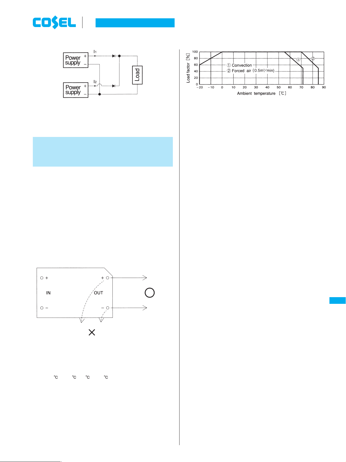
nSeries operation is available by connecting the outputs of two or
more power supplies, as shown below. Output currents in series
connection should be lower than the lowest rated current in each
unit.
But at series operation with same output voltage, diode is not re-
quired to attach even if at (a).
(a) When the output voltage is less than 5V.
D1
Power
supply
Power
supply
D1 - D4: Please use Schottky Barrier Diode.
(b) When the output voltage is more than 12V.
+
-
+
-
D3
D2
Load
D4
(a) (b)
+VIN
DC IN
-VIN
Fig.3.4 Reverse input voltage protection
+VIN
DC IN
-VIN
D1 D2: Please use Schottky Barrier Diode.
ZU/ZT
lZUS10/ZUW10
nSeries operation is available by connecting the outputs of two or
more power supplies as shown below. Output currents in series
connection should be lower than the lowest rated current in each
unit.
(c)
F-95
Page 4
On-board type
(d)
4.2 Parallel redundancy operation
nParallel redundancy operation is available by connecting the units
as shown below.
12
I , I the rated current value
Instruction anualM
ZU1R5 ZU3 ZU6 ZU10
5 Assembling and
Installation Method
5.1 Installation method
nThe unit can be mounted in any direction. Position them with
proper intervals to allow enough air ventilation. Ambient tempera-
ture around each power supply should not exceed the tempera-
ture range shown in derating curve.
nAvoid placing the DC input line pattern lay out underneath the unit
because it will increase the line conducted noise. Make sure to
leave an ample distance between the line pattern lay out and the
unit. Also, avoid placing the DC output line pattern underneath
the unit because it may increase the output noise. Lay out the pat-
tern away from the unit.
ZU/ZT
YES
NO
Fig.5.1 Pattern wiring
5.2 Derating
nBy derating the output current, it is possible to operate the unit
from -20 to +71 (-20 to +85 at forced air cooling).
nWhen unit mounted any way other than in drawings below, it is re-
quired to consider ventilated environments by forced air cooling
or temperature/load derating. For details, please consult our sales
or engineering department.
F-96
Page 5
On-board type
Instruction anualM
ZU1R5 ZU3 ZU6 ZU10
6 Input Voltage/
Current Range
nWhen a non-regulated source is used as a front end, make sure
that the voltage fluctuation together with the ripple voltage will not
exceed the input voltage range.
nSelect the converter that is able to handle the start-up current (Ip).
Fig.6.1 Input current characteristics
9 Input/Output Pin
n
When too much stress is applied on the input/output pins of the
unit, the internal connection may be weakened. As below Fig.
9.1, avoid applying stress of more than 19.6N (2kgf) on the pins
horizontally and more than 39.2N (4kgf) vertically.
n
The input/output pins are soldered on PCB internally, therefore,
do not pull or bend them with abnormal forces.
n
When additional stress is expected to be put on the input/output
pins because of vibration or impacts, fix the unit on PCB (using sil-
icone rubber or fixing fittings) to reduce the stress onto the in-
put/output pins.
Fig.9.1 Stress onto the pins
7 Cleaning
nCleaning is possible by below listed conditions.
Cleaning method
No.
Classification
1
Water type
2
3
Solvent type
4
No.
1
Varnishing or Ultra
sonic wave
2
3
Varnishing,Ultra sonic
wave, Vapor
4
nDuring cleaning to drying (the condition that cleaning liquid is
soaked into the ink of name plate), do not touch on the surface of
name plate.
nAfter cleaning, dry them enough.
Pine Alpha ST–100S(ARAKAWA CHEMICAL CO.)
Clean Through 750H(KAO Corporation)
IPA
Asahiklin AK–225AES(ASAHI GLASS CO.)
Cleaning method
Cleaning agents
Liquid Temp.
Less than
60
–
Period
Within 5
minutes
Within 2
minutes
8 Soldering
10 Peak Current
(Pulse Load)
nIt is possible to supply the pulse current for the pulse load by con-
necting the capacitor externally at the output side.
ZU/ZT
nFlow soldering : 260 less than 15 seconds.
nSoldering iron : 450 less than 5 seconds.
F-97
Page 6
On-board type
nThe average current Iav of output is shown in below formula.
Iav=Is+
nThe required electrolytic capacitor C is found by below formula.
C=
(Iop - Is) t
T
(Iop - Iav) t
Vo
Instruction anualM
ZU15 ZU25
1 Pin Connection
No. Pin connection Function
+DC INPUT
-DC INPUT
RC
+DC OUTPUT
COMMON
-DC OUTPUT
TRM
lSingle Output
+Side of input voltage
-Side of input voltage
Remote ON/OFF
+Side of output voltage
GND of output voltage (Only applicable for Dual output)
-Side of output voltage
Adjustment voltage range
ZU/ZT
lDual (±) Output
2 Function
2.1 Input voltage
nnIf the wrong input is applied, the unit will not operate properly
and/or may be damaged.
2.2 Overcurrent protection
Overcurrent protection circuit is built-in and comes into effect at
over 105% of the rated current.
Overcurrent protection prevents the unit from short circuit and
over current condition of less than 20 sec.
The unit automatically recovers when the fault condition is
cleared.
F-98
Page 7

On-board type
Instruction anualM
ZU15 ZU25
Fig.2.2 Connection devices outside the power supply
Fig.2.1 Overcurrent protection characteristics
2.3 Overvoltage protection
llSingle Output
The overvoltage protection circuit is built-in and comes into effect
n
at 115 - 140% of the rated voltage. The DC input voltage should
be shut down if overvoltage protection is in operation. The mini-
mum interval of DC recycling for recovery 2 to 3 minutes ( ).
The recovery time depends on input voltage.
Multiple Output
n
By detecting overvoltage condition between +V and -V, overvoltage
protection circuit comes into effect at 115 - 140% of the rated
voltage.The DC input voltage should be shut down if overvoltage
protection is in operation. The minimum interval of DC recycling
for recovery 2 to 3 minutes ( ).
The recovery time depends on input voltage.
Remarks:
Please note that unit's internal components may be damaged if
excessive voltage (over rated voltage) is applied to output termi-
nal of power supply. This could happen when the customer tests
the overvoltage performance of the unit.
Table 2.1 Devices outside the power supply (Adjustable ±5%)
No.
1
2
3
4
5
Output
voltage
3V
5V
12V
±12V
±15V
The constant value of devices outside the power supply
VR
1K
1K
5K
5K
5K
R1
470
100
270
10K
10K
(Unit: )
R2
150
270
2.7K
3.9K
2.7K
2.5 Remote ON/OFF
nThe ground terminal of remote ON/OFF circuit is connected with
-V input terminal.
Between RC and -V input: Output voltage is ON at ”Low” level or
short circuit (0 - 1.2V)
Between RC and -V input: Output voltage is OFF at ”High” level
or open circuit (2.4 - 5.5V)
(Connection example)
or or
Transistor IC Relay
ZU/ZT
2.4 Adjustable voltage range
n
The output voltage is adjustable by external potentiometer.
n
When the output voltage adjustment is not used, open the TRM
pin.
n
The over voltage protection circuit comes into effect when the out-
put voltage is set too high.
n
Output voltage is increased by turning potentiometer clockwise
and is decreased by turning potentiometer counterclockwise.
n
The wiring to the potentiometer should be as short as possible
and connected to the remote sensing pins (+S and -S).
The temperature coefficient varies depending on the type of re-
sistor and potentiometer.
It is recommended that the following types be used.
Resistor ...........Metal film type. coefficient of less than ±300ppm/
Potentiometer..Cermet type, coefficient of less than ±100ppm/
When RC terminal is ”Low” level, fan out current is 1mA typ.
When Vcc is applied, use 5V Vcc 24V. When remote ON/OFF
function is not used, please short between RC and -V input.
2.6 Isolation
nFor a receiving inspection, such as Hi-Pot test, gradually increase
(decrease) the voltage for the start (shut down). Avoid using Hi-
Pot tester with the timer because it may generate voltage a few
times higher than the applied voltage, at ON/OFF of a timer.
F-99
Page 8

On-board type
3 Wiring to Input/
Output Pin
nnThe input filter is built-in. A capacitor (Ci),if installed near the in-
put terminal, will lower the input conducted noise from converter
due to the formation of the type filter.
When the distance from the DC line to the unit is greatly ex-
tended, it makes the input feedback noise much higher and the in-
put voltage several times higher than the normal level when
turned ON. If this happens, the output power also becomes un-
stable. In order to prevent the unit form failing in this way; please
connect Ci to the input terminal. In addition, when the filter with
””
L is used, please connect Ci to the input terminal.
Instruction anualM
ZU15 ZU25
nWhen the distance between load and DC output is long, please in-
stall capacitor at load as below.
Fig.3.3 Connection method of capacitor at load
Reverse input voltage protection
n
Avoid the reverse polarity input voltage. It will damage the power
supply.
It is possible to protect the unit from the reverse input voltage by
installing an external diode as shown in Fig.3.4.
(a) (b)
+VIN
DC IN
-VIN
+VIN
DC IN
-VIN
Fig.3.1 Connection method of capacitor at input terminal
Capacity of external capacitor at input terminal: Ci [µF]
Model ZUS15
Input voltage (V)
3, 5
12
24
48
nTo decrease the ripple voltage further, install an external capaci-
tor Co at output terminal as shown below.
ZUW15
330
150
68
33
ZUW25
ZU/ZT
ZUS ZUW
Fig.3.2 Connecting method of external capacitor at output terminal
Capacity of external capacitor at output terminal: Co [µF]
Model ZUS15
Output voltage(V)
3, 5
12
15
ZUW15
220
100
100
ZUW25
ZUS25
470
220
100
47
ZUS25
220
100
100
Fig.3.4 Reverse input voltage protection
4 Series Operation and
Parallel Operation
4.1 Series operation
nSeries operation is available by connecting the outputs of two or
more power supplies, as shown below.
Output currents in series connection should be lower than the low-
est rated current in each unit.
(a) (b)
4.2 Parallel redundancy operation
nnParallel redundancy operation is available by connecting the units
as shown below.
Values of I and I become unbalanced by a slight different of the
output voltage. Make sure that the output voltage of units is of
equal value and the output current from each power supply does
not exceed the rated current.
12
12
I , I the rated current value
F-100
Page 9
On-board type
nUse external potentiometer is recommended which can adjust the
output voltage.
5 Assembling and
Installation Method
5.1 Installation method
nnThe unit can be mounted in any direction. Position them with
proper intervals to allow enough air ventilation. Ambient tempera-
ture around each power supply should not exceed the tempera-
ture range shown in derating curve.
Avoid placing the DC input line pattern lay out underneath the unit
because it will increase the line conducted noise. Make sure to
leave an ample distance between the line pattern lay out and the
unit. Also, avoid placing the DC output line pattern underneath
the unit because it may increase the output noise. Lay out the pat-
tern away from the unit.
Instruction anualM
Fig.5.2 Derating curve
YES
NO
Fig.5.1 Pattern wiring
5.2 Derating
nnBy derating the output current, it is possible to operate the unit
from -20 to +71 (-20 to +85 at forced air cooling).
When unit mounted any way other than in drawings below, it is re-
quired to consider ventilated environments by forced air cooling
or temperature/load derating. For details, please consult our
sales or engineering departments.
ZU/ZT
F-101
Page 10

On-board type
ZU15 ZU25
Instruction anualM
nThe temperature increase of case surface at full load is shown by
below table as referenced data.
Temperature increase on surface of case (ZU series) (Unit: deg)
Input Voltage Output Voltage
5V
12V
24V
48V
5V
12V
±12V
±15V
5V
12V
±12V
±15V
5V
12V
±12V
±15V
5V
12V
±12V
±15V
15W 25W
30
36
39
38
28
34
36
35
31
38
34
27
21
23
24
26
38
42
39
40
36
42
43
45
32
38
36
35
28
25
31
31
6 Input Voltage/
Current Range
nnWhen a non-regulated source is used as a front end, make sure
that the voltage fluctuation together with the ripple voltage will not
exceed the input voltage range.
Select the converter that is able to handle the start-up current (Ip).
nnCleaning period : The total time of varnishing, ultrasonic wave and
vaper should be within 2 minutes. In case of ul-
trasonic wave cleaning, the ultrasonic should be
less than 15kw/m . During cleaning to drying
(the condition that cleaning liquid is soaked into
the ink of name plate), do not touch on the sur-
face of name plate.
After cleaning, dry them enough.
3
8 Soldering
nnFlow soldering : 260 less than 15 seconds.
Soldering iron : 450 less than 5 seconds.
9 Input/Output Pin
n
When too much stress is applied on the input/output pins of the
unit, the internal connection may be weakened. As below Fig.
9.1, avoid applying stress of more than 19.6N (2kgf) on the pins
horizontally and more than 39.2N (4kgf) vertically.
n
The input/output pins are soldered on PCB internally, therefore,
do not pull or bend them with abnormal forces.
n
When additional stress is expected to be put on the input/output
pins because of vibration or impacts, fix the unit on PCB (using sil-
icone rubber or fixing fittings) to reduce the stress onto the in-
put/output pins.
ZU/ZT
nCleaning agents :
F-102
Fig.6.1 Input current characteristics
7 Cleaning
No.
Classification
1
Water type
2
3
Solvent type
4
Pine Alpha ST-100S(ARAKAWA CHEMICAL CO.)
Clean Through 750H(KAO Corporation)
IPA
Asahiklin AK-225AES(ASAHI GLASS CO.)
Fig.9.1 Stress onto the pins
Cleanig agents
Page 11

On-board type
Instruction anualM
ZU15 ZU25
10 Peak Current
(Pulse Load)
nIt is possible to supply the pulse current for the pulse load by con-
necting the capacitor externally at the output side.
ZT1R5 ZT3
1 Pin Connection
-V+V +V
IN OUT
No. Pin connection Function
-DC INPUT
+DC INPUT
Case Connecting
Pin
+DC OUTPUT
NC (Single output)
COM (Dual output)
-DC OUTPUT
-Side of input voltage
+Side of input voltage
If connected to -side of input, the case potential can be
fixed and the value of radiation noise can be reduced.
+Side of output voltage
No Connection
GND of output voltage (Only applicable for Dual output)
-Side of output voltage
S
NC
COM
-V
nThe average current Iav of output is shown in below formula.
Iav=Is+
nThe required electrolytic capacitor C is found by below formula.
C=
(Iop - Is) t
T
(Iop - Iav) t
Vo
lSingle Output
lDual (±) Output
ZU/ZT
lCase Connectiong Pin
Case connecting pin is available. By connecting the pin to -side of
input, the radiation noise from main body can be reduced.
2 Function
2.1 Input voltage
nIf the wrong input is applied, the unit will not operate properly
and/or may be damaged.
F-103
Page 12

On-board type
ZT1R5 ZT3
2.2 Overcurrent protection
nnOvercurrent protection circuit is built-in and comes into effect at
over 105% of the rated current.
Overcurrent protection prevents the unit from short circuit and
over current condition of less than 20 sec. The unit automatically
recovers when the fault condition is cleared.
The power supply which has a current foldback characteristics
may not start up when connected to nonlinear load such as lamp,
motor or constant current load. See the characteristics below.
: Load characteristics of power supply
: Characteristics of load (lamp, motor, constant current load, etc.)
Note: In case of nonlinear load, the output is locked out at A point.
Fig.2.1 Current foldback characteristics
2.3 Isolation
nFor a receiving inspection, such as Hi-Pot test, gradually increase
(decrease) the voltage for the start (shut down). Avoid using Hi-
Pot tester with the timer because it may generate voltage a few
times higher than the applied voltage, at ON/OFF of a timer.
Instruction Manual
Fig.3.1 Connecting method of capacitor at input terminal
Capacity of external capacitor at input terminal: Ci [µF]
Model ZTS1R5
Input voltage(V)
5
12
24
48
nTo lower the output ripple voltage further, install an external ca-
pacitor Co at output terminal as shown below.
ZTS ZTW
Fig.3.2 Connecting method of external capacitor at output terminal
Capacity of external capacitor at output terminal: Co [µF]
Model ZTS1R5
Output voltage(V)
5
12
15
ZTW1R5
100
47
33
10
ZTW1R5
100
100
100
ZTS3
ZTW3
220
100
47
22
ZTS3
ZTW3
220
100
100
3 Wiring to Input/
ZU/ZT
nnInput filter is built-in. A capacitor Ci, if installed near the input ter-
minal, will lower the input conducted noise from converter due to
the formation of the type filter.
When the distance from the DC line to the unit is greatly ex-
tended, it makes the input feedback noise much higher and the in-
put voltage several times higher than the normal level when
turned ON. If this happens, the output power also becomes un-
stable. In order to prevent the unit form failing in this way; please
connect Ci to the input terminal. In addition, when the filter with
””
L is used, please Ci to the input terminal.
F-104
Output Pin
nWhen the distance between load and DC output is long, please in-
stall capacitor at load as shown below.
Fig.3.3 Connection method of capacitor at load
Reverse input voltage protection
n
Avoid the reverse polarity input voltage. It will damage the power
supply.
It is possible to protect the unit from the reverse input voltage by
installing an external diode as shown in Fig.3.4.
(a) (b)
+VIN
DC IN
-VIN
Fig.3.4 Reverse input voltage protection
+VIN
DC IN
-VIN
Page 13

On-board type
ZT1R5 ZT3
Instruction Manual
4 Series Operation and
Parallel Operation
4.1 Series operation
nSeries operation is available by connecting the outputs of two or
more power supplies, as shown below. Output currents in series
connection should be lower than the lowest rated current in each
unit.
But at series operation with same output voltage, diode is not re-
quired to attach even if at (a).
(a) When the output voltage is less than 5V.
D1
Power
supply
Power
supply
D1 - D4: Please use Schottky Barrier Diode.
(b) When the output voltage is more than 12V.
+
-
+
-
D3
D2
Load
D4
5 Assembling and
Installation Method
5.1 Installation method
nnThe unit can be mounted in any direction. Install the device, with
proper intervals to allow enough air ventilation.
5.2 Derating
Ambient temperature around each power supply should not ex-
ceed the temperature range shown in derating curve.
100
Convection[ 1 models]
Convection[Other models]
50
Load factor [%]
Forced air(500 /min)[ 1 models]
Forced air(500 /min)[Other models]
D1, D2: Please use Schottky Barrier Diode.
4.2 Parallel redundancy operation
nParallel redundancy operation is available by connecting the units
as shown below.
12
I , I the rated current value
0
-20 0 102030405060
Ambient temperature [ ]
1 ZTS30512, ZTS30515
ZTW30512, ZTW30515
(71) (85)
70 80 90-10
6 Input Voltage/
Current Range
nnWhen a non-regulated source is used as a front end, make sure
that the voltage fluctuation together with the ripple voltage will not
exceed the input voltage range.
Select the converter that is able to handle the start-up current (Ip).
ZU/ZT
Fig.6.1 Input current characteristics
F-105
Page 14

On-board type
ZT1R5 ZT3
7 Cleaning
nCleaning is possible by below listed conditions.
Cleaning method
No.
Classification
1
Water type
2
3
Solvent type
4
No.
nnDuring cleaning to drying (the condition that cleaning liquid is
soaked into the ink of name plate), do not touch on the surface of
name plate.
After cleaning, dry them enough.
Cleaning method
1
Varnishing or Ultra
sonic wave
2
3
Varnishing,Ultra sonic
wave, Vapor
4
Pine Alpha ST–100S (ARAKAWA CHEMICAL CO.)
Clean Through 750H (KAO Corporation)
IPA
Asahiklin AK–225AES (ASAHI GLASS CO.)
Cleaning agents
Liquid Temp.
Less than
60
–
Period
Within 5
minutes
Within 2
minutes
Instruction Manual
A
A part
Less than
9.8N(1kgf)
Less than 19.6N(2kgf)
Fig.9.1 Stress onto the pins
10 Peak Current
Less than
9.8N(1kgf)
8 Soldering
nnFlow soldering : 260 less than 15 seconds.
Soldering iron : 450 less than 5 seconds.
9 Input/Output Pin
nnWhen too much stress is applied on the input/output pins of the
unit, the internal connection may be weakened. As below Fig.9.1,
avoid applying stress of more than 9.8N (1kgf) on the pins hori-
ZU/ZT
zontally and more than 19.6N (2kgf) vertically.
When additional stress is expected to be put on the input/output
pins because of vibration or impacts, fix the unit on PCB (using sil-
icone rubber or fixing fittings) to reduce the stress onto the in-
put/output pins.
(Pulse Load)
nIt is possible to supply the pulse current for the pulse load by con-
necting the capacitor externally at the output side.
nThe average current Iav of output is shown in below formula.
F-106
Iav=Is+
nThe required electrolytic capacitor C is found by below formula.
C=
(Iop - Is) t
T
(Iop - Iav) t
Vo
 Loading...