

Cosel CHS Series, CHS300-I, CHS400-I, CHS500-I Communications Manual
PMBus communication manual
CHS300/400/500-I
PMBus communication manual
© 2016 COSEL CO.,LTD. ver4.0. 6/15 2016
Applications Manual
1. PMBus interface cable&connection
4. C2 terminal function
5. SMBAlert function
7. Packet error checking
PEC
8. PMBus Hardware specifications
Electrical characters specification on communication terminal
10. PMBus Commands set
CHS300/400/500-I series
1.1
1.2
1.3
1.4
1.5
2. PMBus communication control
2.1
2.2
2.3
2.4
3. Data format
3.1
3.2
4.1
4.2
5.1
5.2
5.3
5.4
6. Explain several functions
6.1
6.2
6.3
6.4
6.5
6.6
6.7
6.8
6.9
6.10
8.1
8.2
9. PMBus software Specifications
9.1
9.2
Terminal function
1.1.1
1.1.2
Terminal function on CHS300-I
Terminal function on CHS400/500-I
How to connect communication
Example of cabling pattern on PMBus communication
PMBus communication pull-up resistor value
Address setting
Overview of control block
RAM (Random Access Memory)
ROM (Random Access Read Only Memory)
Retain the number of abnormal power supply stopping
Data format for output voltage
Data format for another parameter
Power_Good function
Secondary side remote control function
SMBAlert terminal connecting
Checking salve for SMBAlert signal
In case multiple slave devices issue SMB Alert signal
How to do when SMB alert is issued repeatedly
ON/OFF operation
Start-stop voltage
Start-up sequence (start-up delay / rising up)
Setting output voltage
Protective operation for output overvoltage
Protective operation for output undervoltage
Protective operation for overtemperature
Protective operation for undertemperature
Protecting operation for over start-up time
Prohibit re-writing parameter
((((
))))
Ultimate maximum rate on communication terminal
List of PMBus command
PMBus command setting / reading value
Page
2
2
2
3
4
4
5
5
6
6
6
7
7
8
8
8
9
9
9
10
10
10
11
11
12
12
12
13
13
14
14
15
15
17
17
18
19
19
19
20
20
23
25
- 1 -
2.1
Pin configuration
Applications manual
For CHS300/400/500-I series
The PMBus can be used to control and monitor the CHS300/400/500 converter.
For detail, refer to PMBus standard spec manual :
Part I (Revision1.2) and Part II (Revision1.2).
1. PMBus communication cabling and connection
1.1 Terminal function
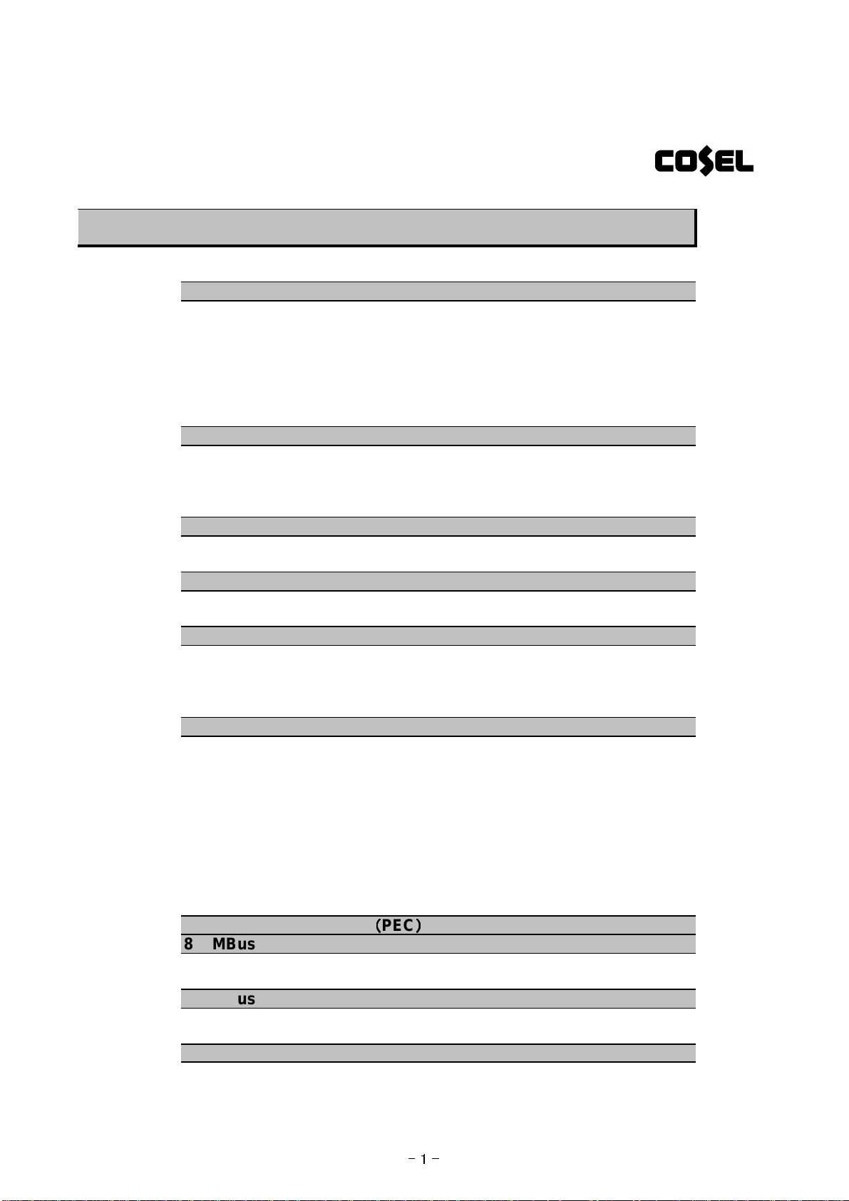
1.1.1 Terminal function on CHS300-I
The figure and the table below show terminal function and name of pins on CHS300-I.
PMBus Power System Management Protocol Specification
#
1
2
3
4
5
6
7
8
9
10
11
12
13
15
Figure 1-1.1. pin assignment in CHS300-I (top view)
Table 1-1.1. Pin Descriptions on CHS300-I
name
Input
terminal
Output
terminal
PMBus
communication
terminal
+VIN
RC
-VIN
+VOUT
+S
TRM
-S
-VOUT
Addr0
NC
Clock
SMBAlert
Data
Sig_GND14
C2
DC input(+)
Remote control (first side
DC input(-)
DC output (+)
Remote sensing (+)
Output voltage adjustment
Remote sensing (-)
DC output (-)
Address setting
Not connected
PMBus communication clock input
Alarm output
PMBus communication data input&output
PMBus communication signal ground
Power_Good or remote control (secondary side
Notefunction
)
)
- 2 -
Applications manual
For CHS300/400/500-I series
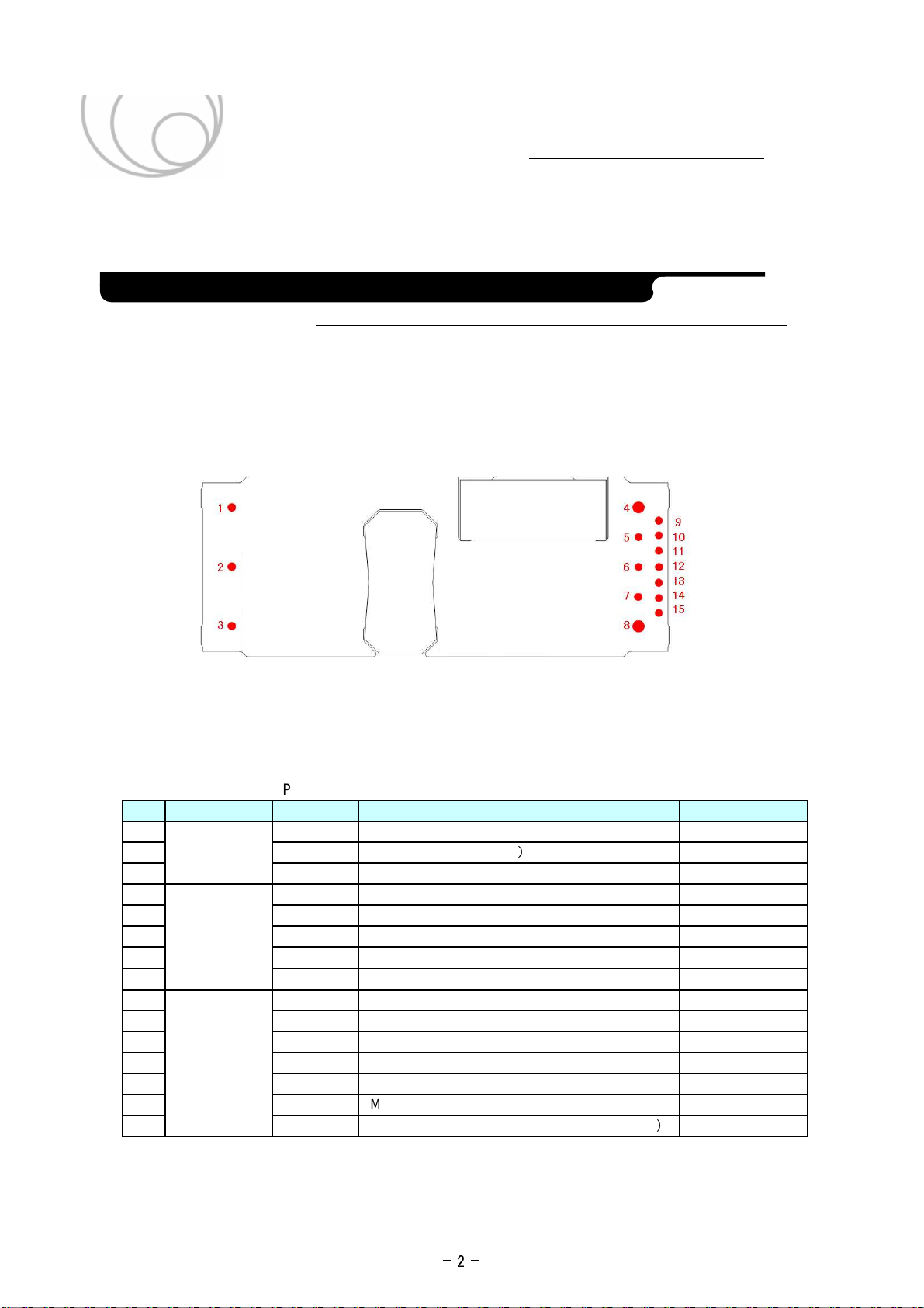
1.1.2 Terminal function on CHS400/500-I
The figure and the table below show terminal function and name of pins on CHS400/500-I.
Figure 1-1.2. pin assignment in CHS400/500-I (top view)
Table 1-1.2. Pin Descriptions on CHS400/500-I
# name
1
2
Input
terminal
3 -VIN
4
5
6 TRM
Output
terminal
7 -S
8
9
10
11
12 SMBAlert
13 Data
PMBus
communication
terminal
14 Sig_GND
15 C2
+VIN
RC
+VOUT
+S
-VOUT
Addr0
Addr1
Clock
*1:
Do not use when adjusting output voltage with PMBus communication.
function
DC input(+)
Remote control (first side
DC input(-)
DC output (+)
Remote sensing (+)
Output voltage adjustment
Remote sensing (-)
DC output (-)
Address setting
Address setting
PMBus communication clock input
Alarm output
PMBus communication data input&output
PMBus communication signal ground
Power_Good or remote control (secondary side
)
Note
*1
)
- 3 -
Applications manual
For CHS300/400/500-I series
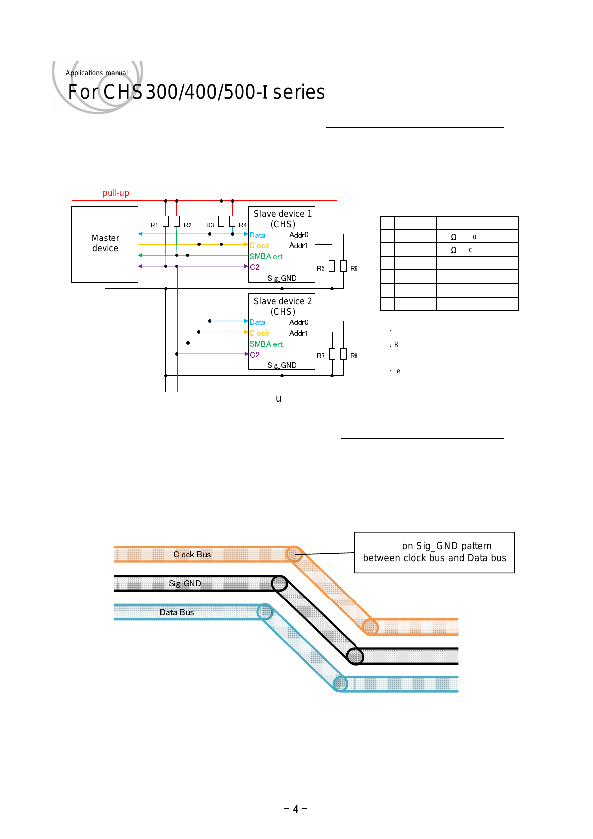
1.2 PMBus Communication connections method
The figure and table below show recommended resistors value for hard wiring PMBus addresses.
pull-up
プルアップ電圧
マスター
デバイス
Master
device
●●●
R1 R2 R3 R4
● ●
●
●
●
●
●
●
●
●
●●
スレーブデバイス1
Slave device 1
(CHS)
●
●
(CHS)
Data Addr0
Clock
Addr1
SMBAlert
C2
R5 R6
Sig_GND
●
スレーブデバイス2
Slave device 2
(CHS)
●
Data
Clock
(CHS)
Addr0
Addr1
●
SMBAlert
C2
R7 R8
Sig_GND
●●
component
#
R1
1
R2
2
R3
3
R4
4
R5,R7
5
R6,R8
6
*1: Connecting C2 as Power-Good function
*2: Refer to clause 1.4 PMBus communication
pull-up resistor
*3: refer to clause 1.5 address setting
Setting value
10kΩ (recommend) *1
10kΩ (recommend) *2
*
2
*
2
*
3
*
3
Figure 1-2 PMBus interface cable chart
1.3 PMBus communication cable pattern example
When connecting the PMBus communication cable, please make sure design to minimize
noise from outside and crosstalk by positioning Sig_GND between Data bus and Clock bus
as shown figure 1-3.
Also, do the right setting for pull-up resistor as parasitic capacitance is happened by way of
shielding and length of cabling. (refer to clause 1.4)
Clock Bus
Sig_GND
Data Bus
Position Sig_GND pattern
between clock bus and Data bus
Figure 1-3 Pattern example
- 4 -
Resistors with 1% tolerance are recommended.
*1 *
2
Applications manual
For CHS300/400/500-I series
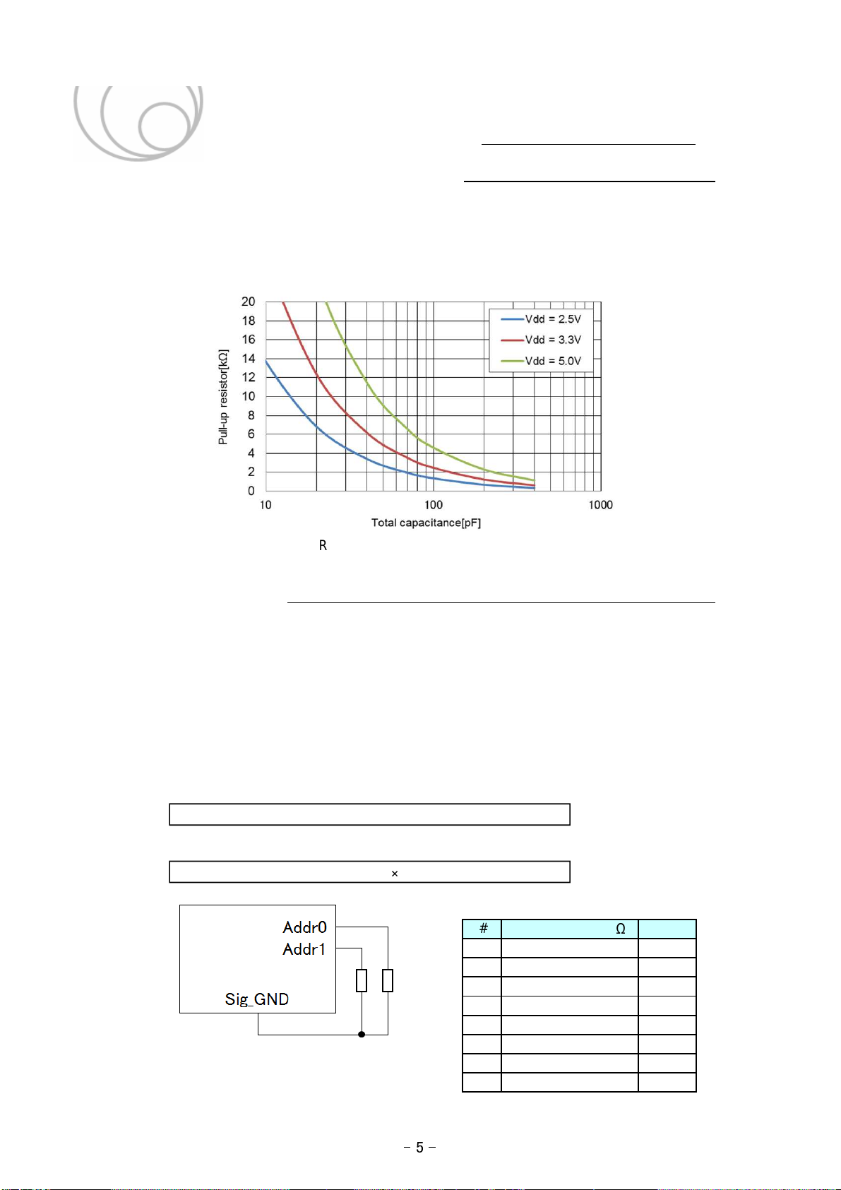
1.4 PMBus communication pull-up resistor value
It is necessary to connect pull-up resistor on Data bus and Clock bus terminal of PMBus .
Recommended value of resistor(maximum value) is shown at figure 1-4.
Note1: Do not exceed the rated output current of converter's terminal (clause 8-1).
Note2: Total of parasitic capacitance and input capacitance should be less 400pF.
Figure 1-4 Recommended value of pull-up resistor
1.5 address setting
The figure and table below show recommended resistors value for hard wiring PMBus addresses.
Take 0-7 on Addr0, Addr1 per value of resistor and address could be assigned 0-63 per
below formula. when calculation result in 0-12,40,44,45,55 setting, address 127 will be return.
*1: Address setting could not be changed after input voltage is applied .
Be sure to make setting before input voltage is applied.
*2: Addr1 is only CHS400/500-I.
The formula for CHS300-I
Address = 16 + Value(Addr0)
The formula for CHS400/500-I
Address = Value(Addr1) ×8 + Value(Addr0)
Table 1-2 Resistor value
ValueResistor value [kΩ]#
10 01
1
2
3
4
5
6
7
Figure 1-5 Address setting
2
3
4
5
6
7
8 220
15
24
36
56
82
130
- 5 -
2.1
Pin configuration
Applications manual
For CHS300/400/500-I series
2. PMBus communication control
2.1 Overview for Control block
This product has built-in RAM and ROM.
Based on the memory parameter, controlling power supply and PMBus communication
are implemented. Conceptual diagram shown in figure 2-1.
Master device
PMBus
PMBus communication with master device
PMBus Interface
Memory
Read operating status
Recover
Recover
Capture
Default store
Memory
(Data ROM)
User store
Memory
(EEPROM)
STATUS
Memory
ClearRead
Parameter change
Operating
RAM ROM
Operating information Update
Data check
Control
Status
Update
Refer
parameter
Microcontroller
Control Signal
Converter circuit
Sense operating information
CHS (Slave device)
Figure 2-1 Conceptual diagram of communication control
2.2 RAM
2.2.1 Operating memory
When power supply is being operated, it refers to setting value of operating memory
with RAM and control it. Since setting change by PMBus communication command is
preserved in operating memory, the setting will be lost after a reset unless they are stored
to data flash.
2.2.2 STATUS memory
You can check status of power supply by reading status memory(command [ 78h ]-[ 7Eh ]).
Corresponding bit on Status memory is set to 1 when power supply has something abnormal.
It will be clear by implementing command of CLEAR_FAULTS [ 03h ], blocking input voltage,
stopping ON/OFF operation (refer to clause 6.1).
- 6 -
Please do not insulate input voltage over 3 seconds when command is being implemented.
Applications manual
For CHS300/400/500-I series
2.3 ROM
2.3.1 DEFAULT STORE MEMORY
Default store memory preserves initial parameter in factory shipment.
Restored information to operating memory is being done by implementing
RESTORE_DEFAULT_ALL [ 12h ] command. *1
2.3.2 USER STORE MEMORY
It is memory to preserve the content of operating memory rewritten by master device after input
voltage after input voltage is insulated. Information is restored by implementing
RESTORE_USER_ALL [ 16h ] command and when power supply is started-up. *1
Information within operating memory is preserved in user store memory by implementing
STORE_USER_ALL [ 15h ] command. *2
*1: Valid only for power supply operation is stopped.
Cannot receive command when power supply is operated. SMBAlert is operated.
*2:
Operating memory
_RAM
Restore
RESTORE_DEFAULT_ALL [12h]
Restore
RESTORE_USER_ALL [16h]
Store
STORE_USER_ALL [15h]
Default store memory
(Data ROM)
User store memory
(EEPROM)
Figure 2-2 Restore and preserving operation for command and parameter
2.4 Retaining the number of protecting operation
When each protective function are operated, the number of information(0-255times) is
preserved in ROM. Command shown in table 2-1 can read the number of protective
operation and delete the number of counts.
Table 2-1 Reading command for the number of stopping abnormal power supply
#
MFR_READ_VOUT_OV_FAULT_COUNT
1
MFR_READ_VOUT_UV_FAULT_COUNT
2
MFR_READ_OT_FAULT_COUNT
3
MFR_READ_UT_FAULT_COUNT
4
MFR_READ_TON_MAX_FAULT_COUNT
5
MFR_READ_VIN_OV_FAULT_COUNT
6
MFR_READ_VIN_UV_FAULT_COUNT
7
MFR_CLEAR_FAULT_CNT
8
Note: In case response of protective operation is auto recovery, it is counted every time
this function is operated after recovery.
Command Code Note
F0h
F1h
F2h
F3h
F4h
F8h
F9h
F5h
Read the number of overvoltage protective operation
Read the number of low output voltage protective operation
Read the number of overheating protective operation
Read the number of low temperature protective operation
Read the number of over star-up time protective operation
Read the number of over input voltage protective operation
Read the number of low input voltage protective operation
Reset the number of operation at F0h~F7h to "00h".
ROM_
- 7 -
3.2 Other
except output voltage
data format
2.1
Pin configuration
N
VALUE = Y ・ 2
Applications manual
For CHS300/400/500-I series
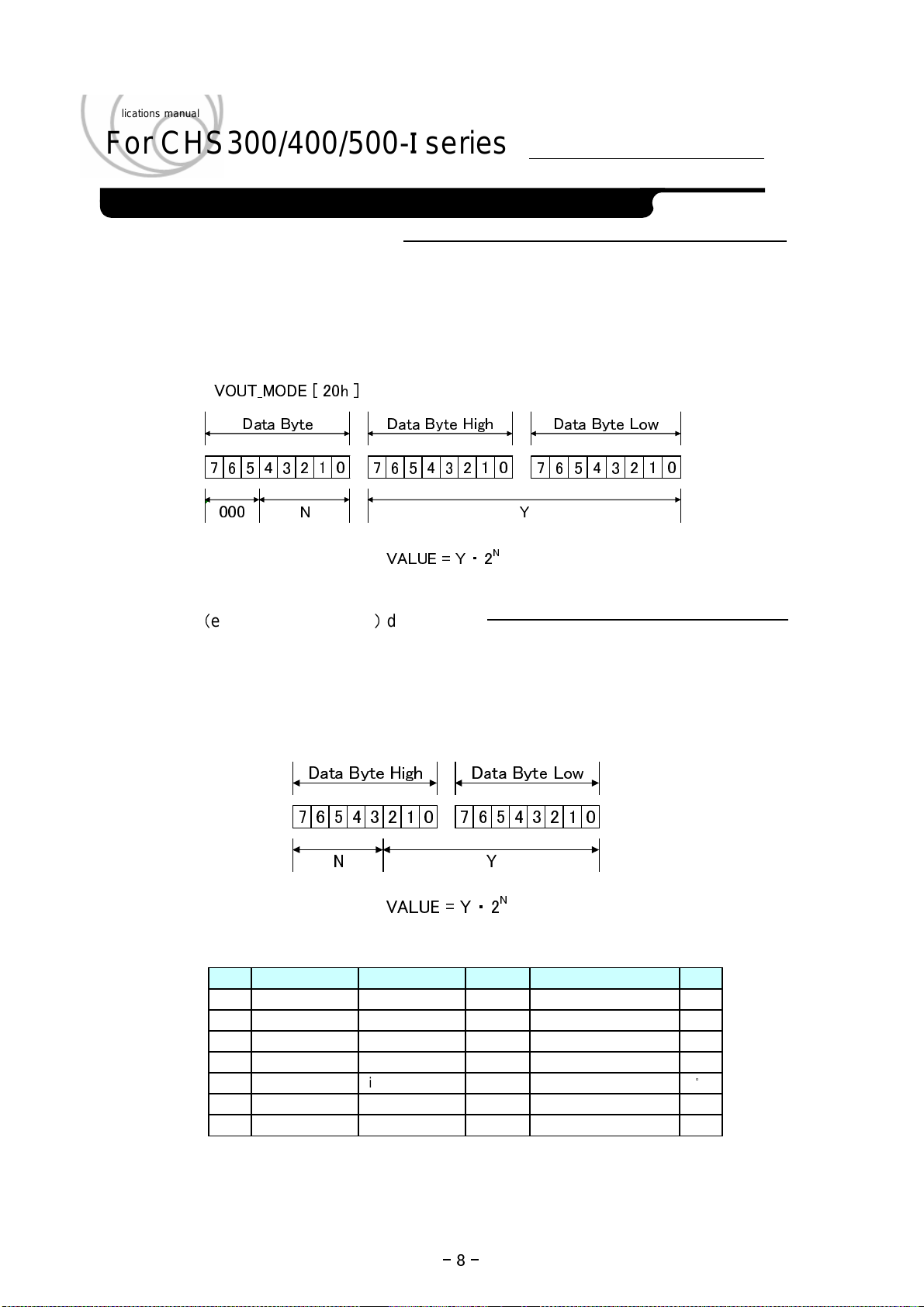
3. Data format
3.1 Data format for output voltage
Please set output voltage and read per shown linear format below.
Data byte Low 5 bit of VOUT MODE [ 20h ] is complement notation by 2 and represents
index part N with code and is fixed -12.
Mantissa part Y is represented 16 bit data without code.
VOUT_MODE [ 20h ]
Data Byte
7 6
000
N Y
(
In compliance with below linear format, please make setting and reading.
Date dyte High 5 bit is complement notation by 2 and represents index part N with code
and varies with data. Mantissa part Y is complement notation by 2 with code and
represents 11 bit data. *1
Data Byte High
)
10 04 3 2 17 67 6
03 25 45 4 3 2
N
Data Byte Low
51
Data Byte High Data Byte Low
3 2 1 07 6 5 43 2 1 07 6 5 4
N Y
VALUE = Y ・ 2
Table 3-1 Index part N value
# Item
1 Output voltage 10100 -12
2 Input voltage
3 Output current 11101 -3 ALinear(Iout)
5 Input wattage 00000
6 Temperature 11110 -2
Starting-up time 11111
7
8 Count
*1: Index part N value is fixed.
Linear(Temp)
Linear(Time)
N(5bit) Characteristics N (*1)
11101 -3 VLinear(Vin)
0
-1
00000 0Linear(Count)
- 8 -
UnitData format
VLinear(Vo)
WLinear(Pin)
C
ms
times

2.1
Pin configuration
Applications manual
For CHS300/400/500-I series
4. C2 Terminal function
C2 terminal can select Power_Good function and remote control (secondary side)function.
Please select function by MFR_C2_ARA_CONFIG [ E0h ] Initial setting is Power_Good function.
4.1 Power_Good function
Power_Good terminal output is open drain. When you use Power_Good function, please
connect C2 terminal with pull-up resistor. Initial setting of Power_Good signal is negative.
(Please make logic setting by MFR_PGOOD_POLARITY [ E2h ])
If output voltage is beyond setting value of POWER_GOOD_ON [ 5Eh ] , C2 terminal
will be low.
If output voltage is lower than the setting value of POWER_GOOD_OFF [ 5Fh ] ,
C2 terminal will be high.
Also, during 10ms in charging input voltage, voltage level on C2 terminal is unstable.
4.2 Remote control (Secondary side) function
Initial setting of Remote control (secondary side) function is negative and is invalid
when you select function.
Selecting logic and setting for invalid or valid function can be made by MFR_C2_LOGIC [ E1h ].
- 9 -
2.1
Pin configuration
Applications manual
For CHS300/400/500-I series
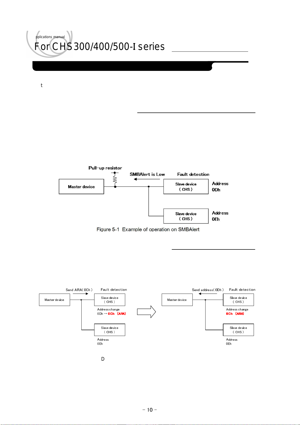
5. Explanation for terminal function of SMBAlert
SMBAlert protocol is also supported by the module. By which the module can alert the PMBus master
that it has an active status or alarm condition.
(Standard manual of SMBus for the details : System Management Bus(SMBus) Specification Ver 2.0)
5.1 Connecting SMBAlert terminal
Output terminal of SMBAlert is open drain. When you use function of SMBAlert,
connect pull-up resistor with SMBAlert terminal.
When something abnormal is happened in slave device, Slave device which detects something
abnormal will make SMBAlert low level.
( URL: http://smbus.org/specs/ )
Figure 5-1 Example of operation on SMBAlert
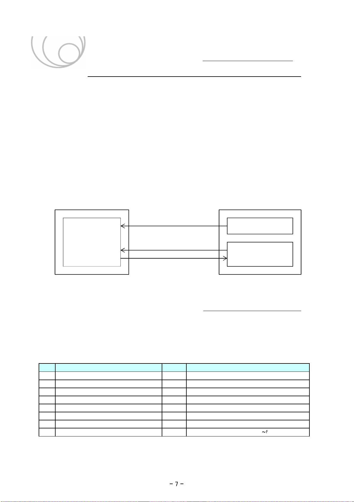
5.2 Identifying slave device issuing SMBAlert signal
Master-device can identify which slave device has something abnormal.
By receiving READ communication (*1) using ARA from master device, power supply
with something abnormal sends original address.
Send ARA( 0Ch )
Master device
*1:
When receiving READ communication using ARA, SMBAlert will be cancelled .
In order to enable the SMBAlert signal, it is necessary to send CLEAR_FAULTS [ 03h ].
Fault detection
Slave device
( CHS )
Address change
0Dh →
0000Ch (ARA)
Ch (ARA)
Ch (ARA)Ch (ARA)
Slave device
( CHS )
Address
0Eh
Master device
Diagram 5-2 Identifying Slave using ARA
Send address( 0Dh )
Fault detection
Slave device
( CHS )
Address change
0000Ch (ARA)
Ch (ARA)
Ch (ARA)Ch (ARA)
Slave device
( CHS )
Address
0Eh
- 10 -

Applications manual
For CHS300/400/500-I series
5.3 In case multiple slave devices issue SMBAlert signal
When multiple slave devices issue SMBAlert single at the same time, it is not possible
to make judgment for slave address by ARA. When you restore, please communicate
by ARA and release with SMBAlert.
5.4 How to do when SMBAlert is issued repeatedly.
When abnormal status such as automatic recovery situation keeps going, SMBAlert is
being operated again by READ communication with using ARA regardless returning
original address.
In case setting is made to response only ARA by MFR_C2_ARA_CONFIG [ E0h ] ,
communication other than ARA is not available as address on power supply is set for
only ARA.
When this situation is on going, normal communication is possible by freeing ARA after
stopping power supply with ON/OFF function (refer to 6.1).
- 11 -
2.1
Pin configuration
Applications manual
For CHS300/400/500-I series
6. Explanation of several functions
6.1 ON/OFF operation
Three ON/OFF functions are available with the CHS300/400/500 as shown in table 6-1.
in order to control starting-up and insulating power supply by external signal.
When either setting is "OFF", power supply will be stopped.
Table 6-1 Output ON/OFF function
# ON/OFF function
1
OPERATION [01h] command ON/OFF function
2
Remote control (primary side) function
3
Remote control (secondary side) function
*1: When operating by positive logics, it is optional.
*2: When invalid setting is made by command, it will be status of "ON" compulsory.
logical setting (initial value)
Negative (invalid for change)
Negative (valid for change)
*1
*2
Note
6.2 Start-stop voltage
Power supply is started-up when the input voltage exceeds set value of VIN_ON [ 35h ] (*1)
and is stopped when falling below set value of VIN_OFF [ 36h ] .
When changing a set value with start-up voltage and stop voltage, have an equal to or more
than 2.5 V hysteresis between VIN_ON [ 35h ] and VIN_OFF [ 36h ] to avoid the operation
which repeats a start-up and a stop.
*1: Be sure to set VIN_ON [ 35h ] > VIN_OFF [ 36h ]
- 12 -

6.3 Start-up sequence
starting-up delay / rising up
Applications manual
For CHS300/400/500-I series
(
)
TON_DELAY [ 60h ] can set start-up delay time until output voltage is risen up after input
condition is met. When setting more shortly than the start-up delay-characteristics of
the power, there is not a change in the start-up delay time.
TON_RISE [ 61h ] command can set. rising up time.(only CHS400-I)
But, when setting is more shortly than the start characteristic of the power, there is not
a change in the start time. (For the details of the value setting, refer to clause 10.)
Figure 6-1 Setting for starting-up sequence (example for Vin start-up)
6.4 Output voltage setting (only CHS400/500-I)
You can set output voltage of power supply by command as shown Table 6-2.
Table 6-2 Function of output voltage setting
# Output voltage setting
VOUT_COMMAND [ 21h ]1
2 VOUT_MARGIN_HIGH [ 25h ] *1
3 VOUT_MARGIN_LOW [ 26h ]
4 VOUT_TRIM [ 22h ]
*1: Switching by OPERATION [ 01h ] command. Initial value is VOUT_COMMAND [ 21h ].
Output voltage becomes value shown in below format.
Output voltage of power supply = VOUT_TRIM [ 22h ] value of setting + or VOUT_MARGIN_HIGH [ 25h ] Value of setting
*1
*1
Please use this as slight adjustment for output voltage.
or VOUT_MARGIN_LOW [ 26h ] Value of setting
Note
VOUT_COMMAND [ 21h ] Value of setting
- 13 -

Applications manual
For CHS300/400/500-I series
6.5 Protective operation for output overvoltage
Output overvoltage protection function is operated when the output voltage becomes high.
The operation threshold and the way of the output over voltage protection function can be
changed respectively at VOUT_OV_FAULT_LIMIT [ 40h ] and
VOUT_OV_FAULT_RESPONSE [ 41h ] . In case the way of stopping latch stop,
Power Supply does not restore until restored operation is done by ON/OFF function(clause 6.1)
or re-invert after insulating input.
When the number of automatic recovery is set by 1-6 times, latch stop will be happened
without situation of abnormal power supply is recovered during re-starting up by specific
number of times.
6.6 Protective operation for output undervoltage
Output undervoltage protection function is operated when the output voltage becomes low.
The operation threshold and the way of the output under voltage protection function can be
changed respectively by VOUT_UV_FAULT_LIMIT [ 44h ] and
VOUT_UV_FAULT_RESPONSE [ 45h ]. In case the way of stopping latch stop,
Power Supply does not restore until restored operation is done by ON/OFF function(clause 6.1)
or re-invert after insulating input.
When the number of automatic recovery is set by 1-6 times, latch stop will be happened
without situation of abnormal power supply is recovered during re-starting up by specific
number of times.
- 14 -
Thermal protection
Applications manual
For CHS300/400/500-I series
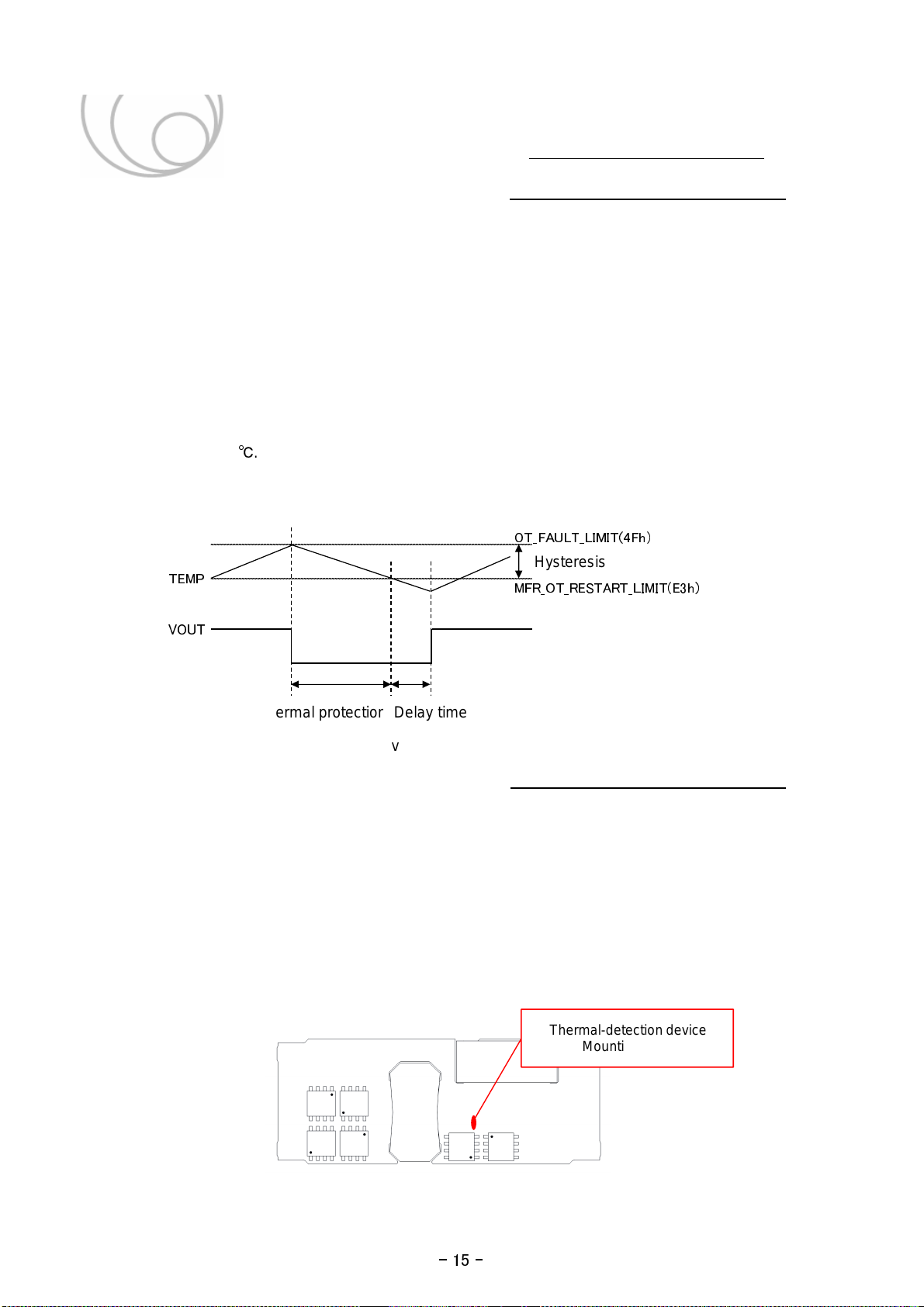
6.7 Protective operation for overtemperature
The overtemperature protection feature works when the temperature detecting-element
temperature which is shown in figure 6-3 becomes high.
In protection operation, power supply will be stopped and re-start via delaying time originally
to be set after abnormal status is cancelled.
The operation threshold and the way of stopping overheating is changed by
OT_FAULT_LIMIT [ 4Fh ] and OT_FAULT_RESPONSE[ 50h ] respectively.
The return temperature of the overheating protection is set to
MFR_OT_RESTART_LIMIT [ E3h ] and status of stopping is canceled by being below
this threshold.
Set temperature difference with operating temperature and return temperature to equal to or
more than 10℃.
In case the way of stopping latch stop, Power Supply does not restore until restored
operation is done by ON/OFF function(clause 6.1) or re-invert after insulating input.
OT_FAULT_LIMIT(4Fh)
ヒステリシス
Hysteresis
TEMP
MFR_OT_RESTART_LIMIT(E3h)
VOUT
過熱保護
遅延時間
Delay time
Figure 6-2. overtemperature protection restart
6.8 Protective operation for undertemperature
The undertemperature protection feature works when the temperature of the temperature
detecting-element which is shown in figure 6-3 becomes low.
The operation threshold and the way of stopping low temperature protection are changed
at UT_FAULT_LIMIT [ 53h ] and UT_FAULT_RESPONSE respectively.
The change of going out is possible.
When making a way of stopping a restart, the return temperature of the low temperature
protection is cancelled by exceeding the threshold which was set
in MFR_UT_RESTART_LIMIT [ E4h ] and then does a restart via the delay time which
is set at UT_FAULT_RESPONSE [ 54h ].
Thermal-detection device
Mounting point
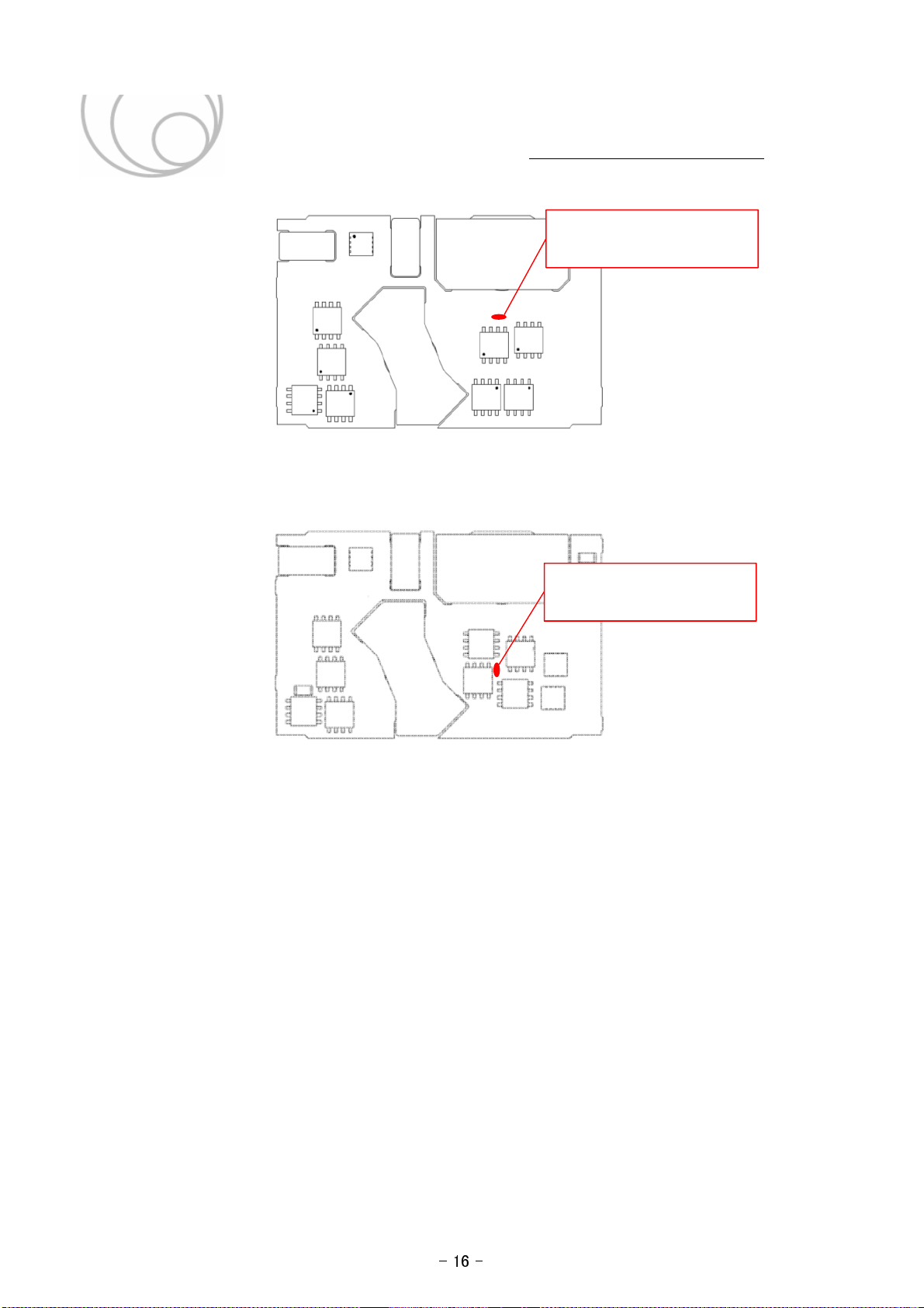
Figure 6-3.1 Temperature measuring point for CHS300-I (top view)
- 15 -
Applications manual
For CHS300/400/500-I series
Figure 6-3.2 Temperature measuring point for CHS400-I (top view)
Thermal-detection device
Mounting point
Thermal-detection device
Mounting point
Figure 6-3.3 Temperature measuring point for CHS500-I (top view)
- 16 -
 Loading...