

Page 1
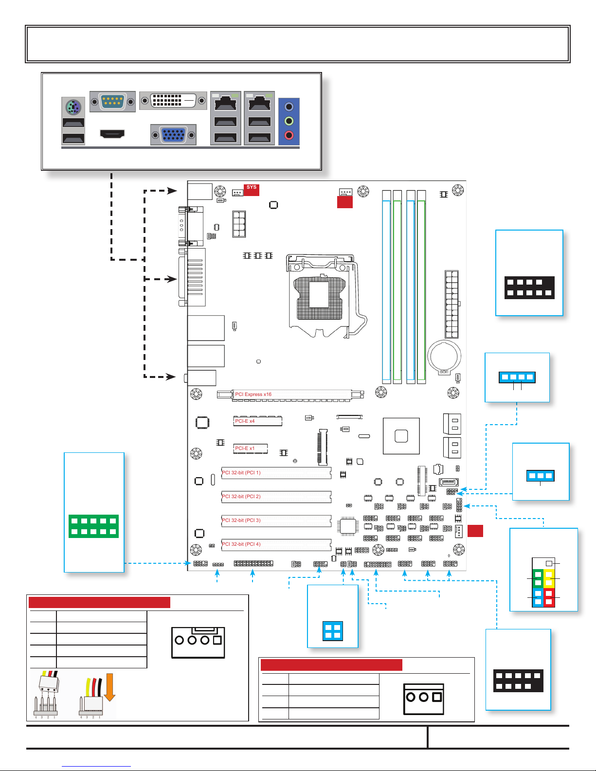
Q67AX Motherboard : Quick Setup and Header Pin Reference
PCI 32-bit (PCI 1)
PCI Express x16
PCI-E x4
PCI-E x1
PCI 32-bit (PCI 2)
PCI 32-bit (PCI 3)
PCI 32-bit (PCI 4)
PS/2
Keyboard
Mouse
USB
x2
Serial 1
HDMI
DVI-D (D)
VGA
LAN
2
USB
x2
SYS
Fan 1
+12V
Input
LAN
USB
ATX
1
x2
Line-IN
Optical
SPDIF Out
Line
Out
Mic
CPU
Fan
ATX Power
Input
MN-Q67AX-Q1
01302012
COM 2-10
RS232
Serial Headers
9
1627384
DCD DSR
5
TX CTS
RX RTS
DTR RI
GND
Front Panel
Audio Headers
(Line Out 2) JD
10
1234567 9
Sense FB
(Mic 2) Left Audio GND -
(Mic 2) Right Audio JD (Presence)
(Line Out 2) Left
(Line Out 2) Right (Mic 2) JD
4 - Pin CPU Fan Connections
ASSIGNMENT
PIN
GND
1
+12V
2
Tachometer
3
PWM
4
When connecting a 3-Pin fan, speed
will not be controlled by system
(100% full speed)
Maximum 350mA (4.2 watts) per fan
Speaker Output
DDR3 1066 / 1333 DIMM Socket 3
DDR3 1066 / 1333 DIMM Socket 1
DDR3 1066 / 1333 DIMM Socket 2
DDR3 1066 / 1333 DIMM Socket 4
VCC
NC NC
4321
SPEAK
Alt. Power
LED
31
+
Alt. Power
Chassis Open
Header
COM3 COM5 COM7 COM9
COM4 COM6 COM8 COM10
SYS
Fan 2
LED
Front Panel
Connections
9
NC
+
8
Power
+
Parallel HeaderCD Audio IN
1234
COM2
RS232
Header
COM2
RS422 / 485
Headers
RX-
43
TX-
21
TX+
RX+
JP9
COM2 Serial Port
Mode Selection
TPM
Trusted Platform
Module
Switch
Power
+
LED
USB Header
Reset
576
4
3
HDD
LED
+
2
1
Connections
3 - Pin Fan Connections
ASSIGNMENT
PIN
GND
1
+12V
2
Tachometer
3
123
1234567
VCC VCC
NC
8
10
GND GND
-DATA - DATA
+DATA + DATA
Note: Pin #1 is identied on the solder side of the motherboard with a square shaped pin.
Q67AX
Page 1
Page 2
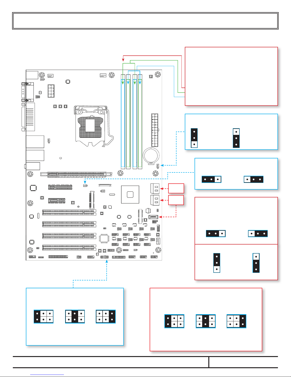
Q67AX Motherboard Family : Quick Setup and Header Pin Reference (continued)
Dual Channel RAM Conguration / Installation:
The Q67AX Motherboard is compatible with
240-pin DDR3 1066 or DDR3/1333 SDRAM Modules
up to 8GB in size. (Max 32GB system memory)
To gain the performance advantage of Dual channel
communication, use matching pairs of DIMM
JP10 PS/2 &
USB Power
JP8
COM1
Voltage
JP5 USB
Power
modules and populate the slots as follows:
One DIMM module - Plug into socket 1
Two DIMM modules - Plug into socket 1 and 3
Four DIMM modules - Install matching pairs into
sockets 1 & 3, and a matching pair into sockets 2 & 4
JBAT: Reset BIOS (CMOS) Settings
Move momentarily to reset CMOS registers
Normal
1
Operation
2
Jumper Position
(default)
3
Power off, and
move jumper here
for several seconds
to reset CMOS
Mini PCIe Slot
JP12 JP14 JP16 JP17
JP13 JP15 JP19 JP18
COM2
JP11
COM2
Voltage
RS232
Header
COM2
RS422 /
RS485
Header
COM3
Voltage
JP9: COM2 RS485 / RS422 Serial Port Mode
Move jumpers to disable COM2 10-pin RS232 headers
and enable COM2 4-Pin RS485/RS422 Headers.
2 4 6
2 4 6
2 4 6
DDR3 1066 / 1333 DIMM Socket 1
DDR3 1066 / 1333 DIMM Socket 2
DDR3 1066 / 1333 DIMM Socket 4
DDR3 1066 / 1333 DIMM Socket 3
JP3 USB
Power
JP20: Mini PCIe Voltage Selection
Move to select Required Mini PCIe Voltage
SATA3 Ports
(x2)
SATA2 Ports
(x3)
VCC = 3.3V
321
JP3: USB Power, JP10: USB & PS/2 Power
VCC = 3.3V SB
Allows port voltage to devices when system is
in standby. Required for a connected device to
wake the computer from sleep / standby.
(JP3 controls USB headers, JP10 & JP5 control
the adjacent external ports)
Standby Power OFF
Standby Power ON
321
JP5: USB Port Power When In Standby
1
2
3
1
2
3
Standby Power OFF Standby Power ON
JP8, JP11-19: Serial COM Port Voltage Output Enable
Move jumpers to disable or select voltage output via pin 9, on
the corresponding COM RS232 headers. Allows compatible
devices to be bus powered via the voltage enabled serial ports.
2 4 6
2 4 6
2 4 6
321
321
1 3 5
COM2
RS232
(default)
1 3 5
COM2
RS485
Mode
1 3 5
Note: Pin #1 is identied on the solder side of the motherboard with a square shaped pin.
COM2
RS422
Mode
1 3 5
No Voltage
Output
(default)
1 3 5
12VDC
Output
Q67AX
1 3 5
5VDC
Output
Page 2
 Loading...