

Page 1
Page 2
User Manual/ Specification September 22, 2013
1
User Manual/ Specification | 9/22/2013
1.0 Initial release
04/11/2013
1.1 Update RF parametric
06/19/2013
1.2 Update timing diagram
07/29/2013
1. All parts and materials must be ROHS compliant. Halogen Free.
2. The module’s RF specifications are complaint with 3GPP
3. All specifications under normal temperature, normal voltage conditions unless otherwise noted
External:
3GPP TS 36.521 version 8.0.1 Release 8
3GPP TS 34.121 version 8.10.0 Release 8
3GPP TS 51.010-1 version 9.2.0 Release 9
Page 3
User Manual/ Specification September 22, 2013
2
User Manual/ Specification | 9/22/2013
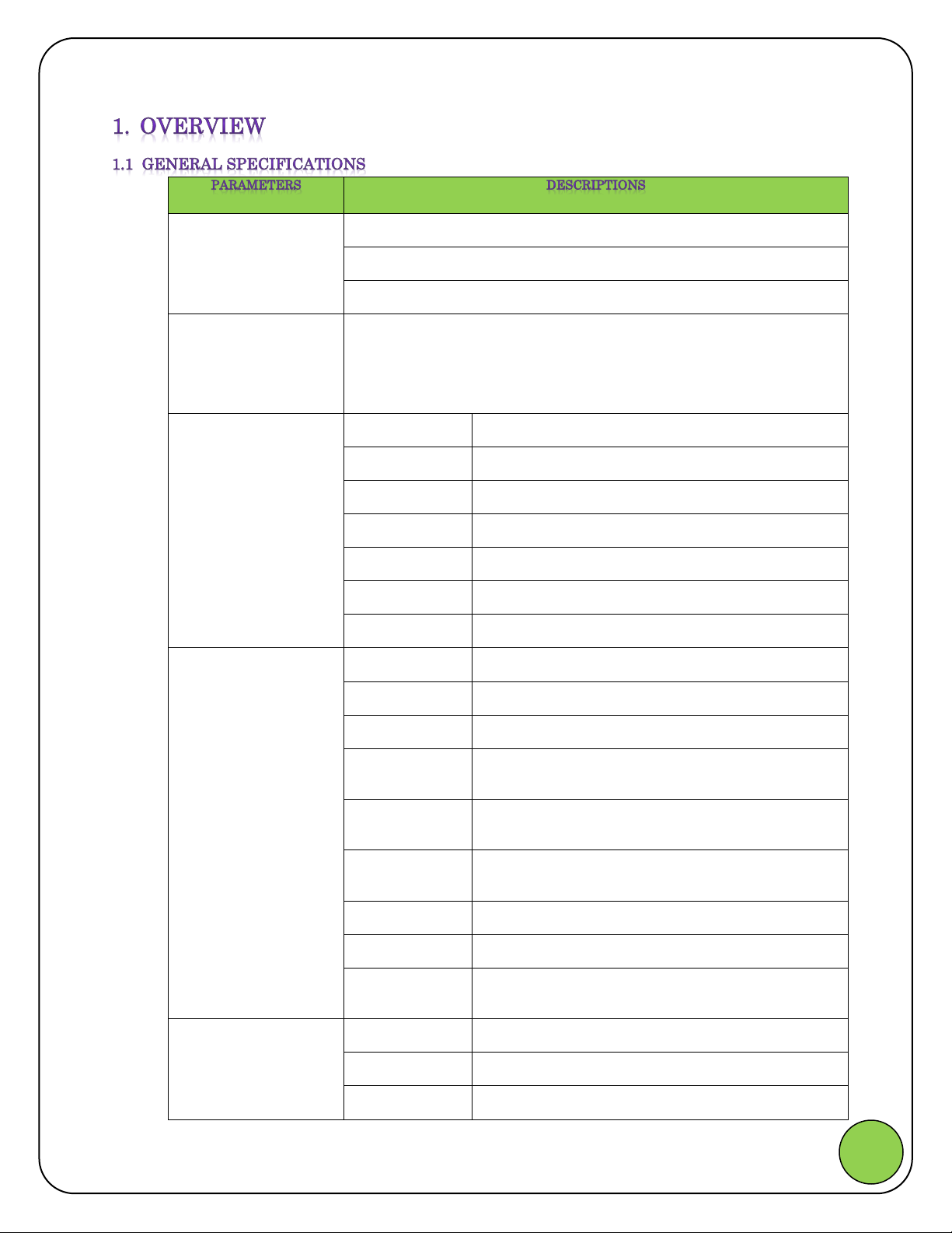
Air Interfaces
WCDMA Band I, V, VIII
GPRS / EDGE 850, 900, 1800
LTE Band III, VII, XX
Protocols
LTE: Rel 8, Cat 3
WCDMA / HSDPA / HSUPA / HSPA+ / DC-HSDPA: Rel 8
GSM / GPRS / EDGE : Rel 6
Max Data Rate
LTE
100 Mbps Down (64QAM) / 50 Mbps Up (16QAM)
DC-HSDPA Cat 24
42.2 Mbps Down
HSDPA Cat 14
21.1 Mbps Down
HSUPA Cat 6
5.76 Mbps Up
WCDMA
384 Kbps Down / Up
GPRS
Multi slot class 10, CS-4 80 Kbps Down / 20 Kbps Up
EDGE
MCS-9, 236.8 Kbps Down / 59.2 Kbps Up
RX / TX Frequency
Interval
LTE Band III
95 MHz
LTE Band VII
120 MHz
LTE Band XX
41 MHz
WCDMA / HSPA
850
45 MHz
WCDMA / HSPA
2100
190 MHz
WCDMA / HSPA
900
45 MHz
GPRS / EDGE 850
45 MHz
GPRS / EDGE 900
45 MHz
GPRS / EDGE
1800
95 MHz
Nominal output power (+/1dB)
LTE Band 3, 20
23 dBm (Power class 3)
LTE Band 7
23.5 dBm (Power class 3)
WCDMA
23 dBm (Power class: 3)
Page 4
User Manual/ Specification September 22, 2013
3
User Manual/ Specification | 9/22/2013
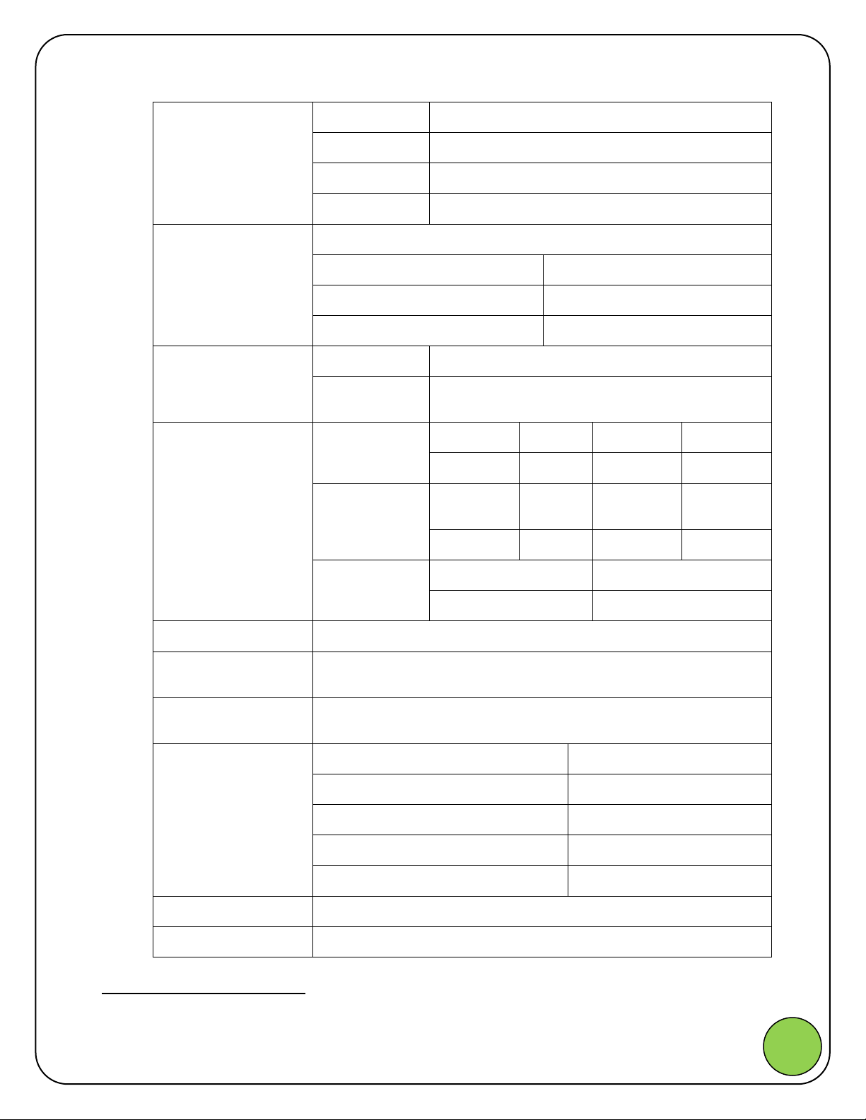
GPRS 850 / 900
32 dBm (Power class: 4)
GPRS 1800
29.5 dBm (Power class: 1)
EDGE 850 / 900
26.5 dBm (Power class: E2)
EDGE 1800
25.5 dBm (Power class: E2)
Operating Voltage
VBATT 3.4V ~ 4.4V
Low voltage
3.4V
Nominal voltage
4.4V
High voltage
4.4V
Sleep / Off Current
Off Leakage
5uA
Rock Bottom
[Sleep]
2mA
Standby Current `
(single cell, no neighbors)
LTE standby
128 Frames
5.15mA
WCDMA standby
64 Frames
128
Frames
256 Frames
512 Frames
5.51mA
4.15mA
3.05mA
2.90mA
GPRS standby
MFRMS = 2
5.8mA
Peak Current
2.0A max, 600µs, 12.5 % Duty Cycle
Operating Temperature
Range
-10°C ~ +55°C
Storage Temperature
Range
-30°C ~ +80°C
Frequency Stability
WCDMA / HSDPA 850
±0.1ppm
WCDMA / HSDPA 900
±0.1ppm
WCDMA / HSDPA 2100
±0.1ppm
LTE Band III, VII, XX
±0.1ppm
GPRS / EDGE
±0.1ppm
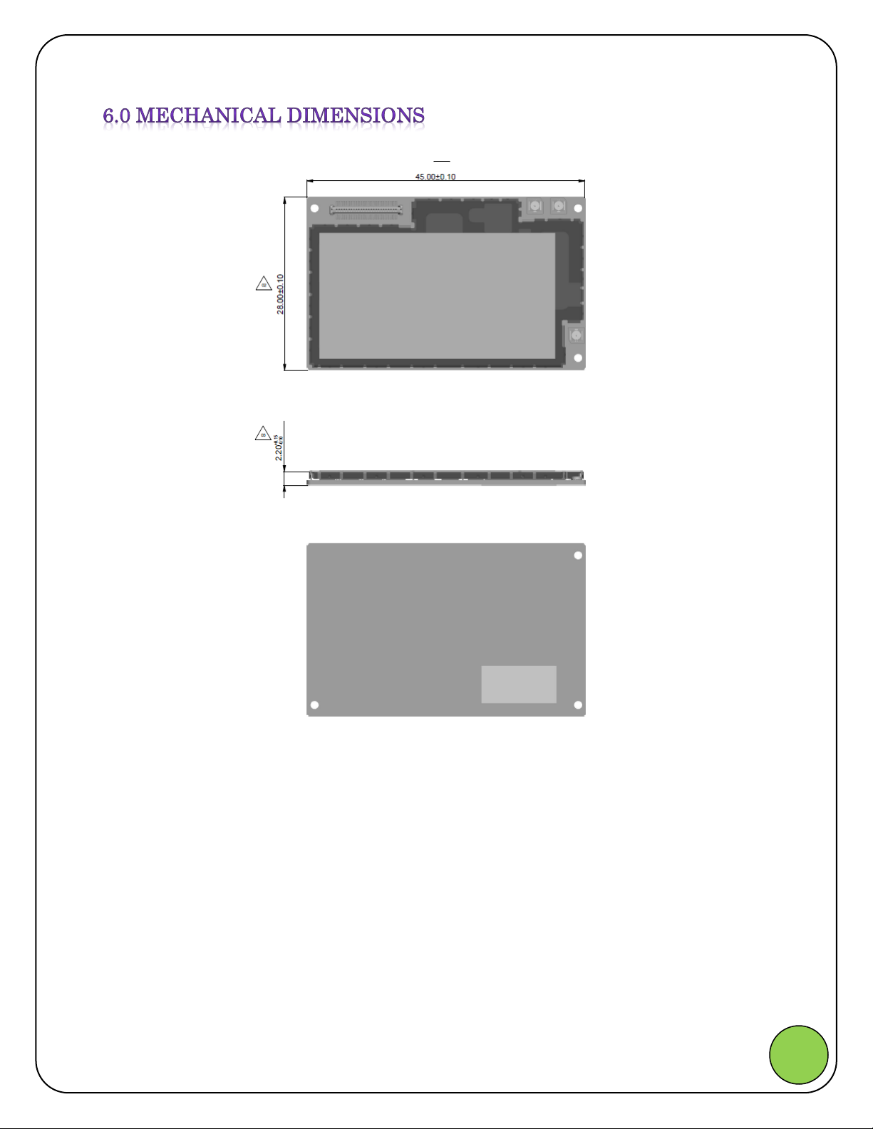
Physical Dimensions1
48.00 x 28.00 x 2.1 mm
Weight
6.9g
Page 5
User Manual/ Specification September 22, 2013
4
User Manual/ Specification | 9/22/2013
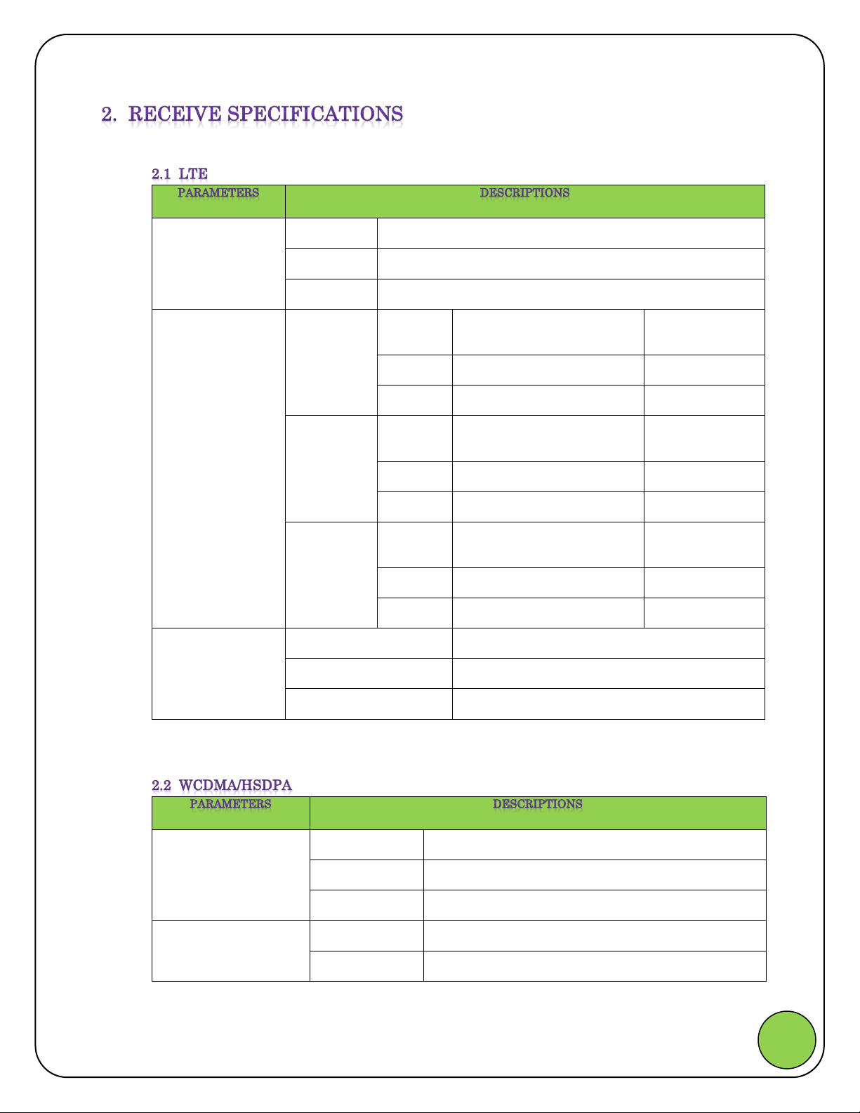
Frequency Range
Band III
[DCS] Down: 1805 ~ 1880 MHz
Band VII
[2.6GHz] Down: 2620 ~ 2690 MHz
Band XX
[Europe 800] Down: 791 ~ 821 MHz
Reference Sensitivity
Level
(PRX and DRX
combined)
Band III
BW (MHz)
PRX and DRX combined
Reference Sensitivity (dBm)
Modulation
10
-94
QPSK
20
-91
QPSK
Band VII
BW (MHz)
PRX and DRX combined
Reference Sensitivity (dBm)
Modulation
10
-95
QPSK
20
-92
QPSK
Band XX
BW (MHz)
PRX and DRX combined
Reference Sensitivity (dBm)
Modulation
5
-97
QPSK
10
-94
QPSK
Adjacent Channel
Selectivity
BW (MHz)
Adjacent Channel Selectivity (dB)
5
33 dB
10
33 dB
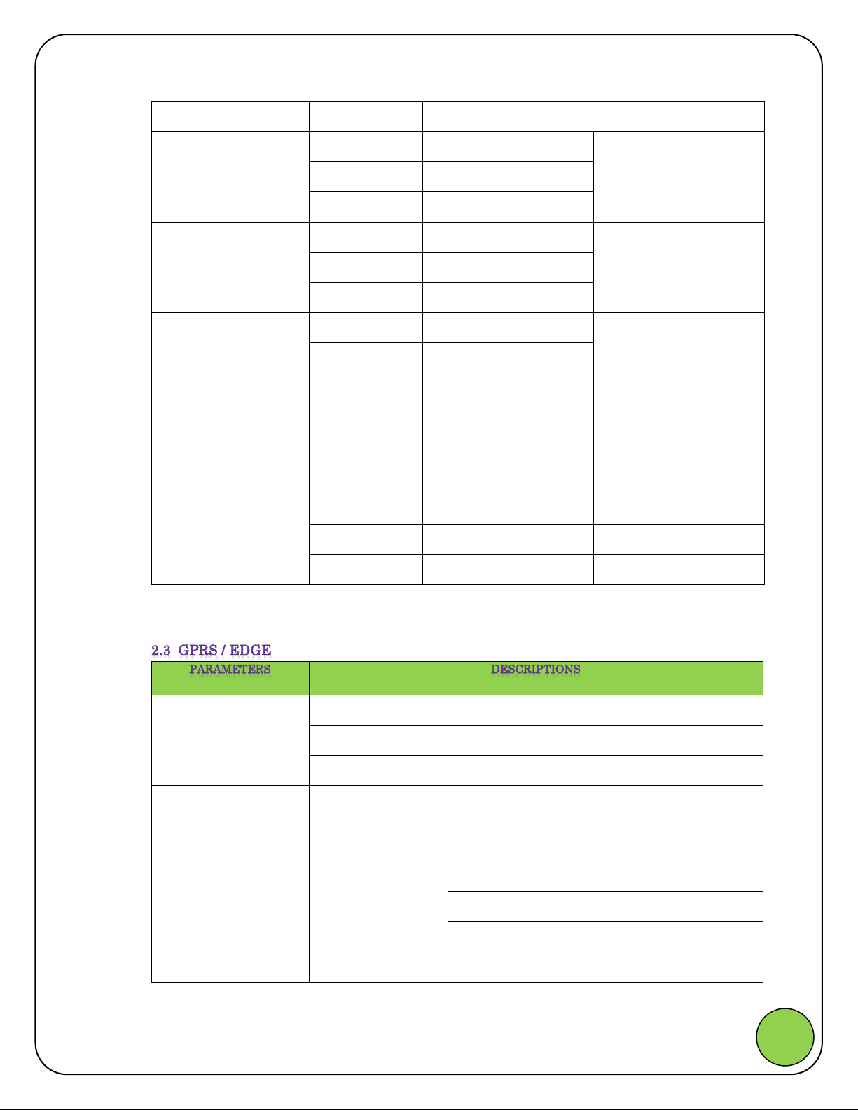
Frequency Range
Band I
[2100] Down: 2110 ~ 2170 MHz
Band V
[850] Down: 869 ~ 894 MHz
Band VIII
[900] Down: 925 ~ 960 MHz
Reference Sensitivity Level
Band I
-106.7 dBm
Band V
-104.7 dBm
Page 6
User Manual/ Specification September 22, 2013
5
User Manual/ Specification | 9/22/2013
Band VIII
-103.7 dBm
Adjacent Channel
Selectivity
Band I
-92.7 dBm
-52dBm @ ±5MHz
Band V
-90.7 dBm
Band VIII
-89.7 dBm
Intermodulation
Band I
-103.7 dBm
-46dBm ±10MHz, ±20MHz
Band V
-101.7 dBm
Band VIII
-100.7 dBm
Spurious Response
Band I
-103.7 dBm
-44 dBm
Band V
-101.7 dBm
Band VIII
-100.7 dBm
In-Band Blocking
Band I
-103.7 dBm
-56 dBm @ ±10MHz, -44 dBm
@ ±15MHz
Band V
-101.7 dBm
Band VIII
-100.7 dBm
Peak throughput
HSDPA
21Mbps
Category 14
DC-HSDPA
42Mbps
Category 24
HSUPA
5.76Mbps
Category 6
Frequency Range
GPRS / EDGE 850
Down: 869 ~ 894 MHz
GPRS / EDGE 900
Down: 925 ~ 960 MHz
GPRS / EDGE 1800
Down: 1805 ~ 1880 MHz
Minimum Input level for
Reference Performance
GPRS 850/900/1800
Type of Channel
Propagation Condition:
BLER < 10%, Static
PDTCH/CS-1
-104 dBm
PDTCH/CS-2
-104 dBm
PDTCH/CS-3
-104 dBm
PDTCH/CS-4
-101 dBm
EDGE 850/900/1800
PDTCH/MCS-5
-98 dBm
Page 7
User Manual/ Specification September 22, 2013
6
User Manual/ Specification | 9/22/2013
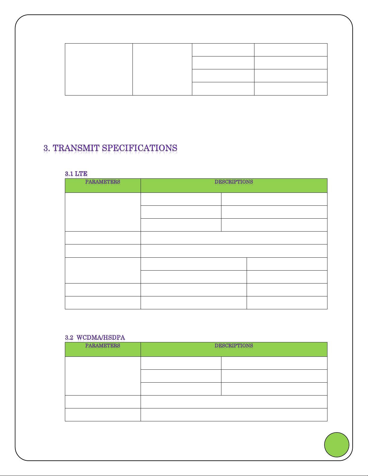
PDTCH/MCS-6
-96 dBm
PDTCH/MCS-7
-93 dBm
PDTCH/MCS-8
-90.5 dBm
PDTCH/MCS-9
-86 dBm
Frequency Range
Band III
[DCS] Up: 1710 ~ 1785 MHz
Band VII
[2.6GHz] Up: 2500 ~ 2570 MHz
Band XX
[Europe 800] Up: 832 ~ 862 MHz
Max Output Power
23dBm ±2 dBm
Min Output Power
Below -40dBm
Error Vector Magnitude
17.5%
QPSK or BPSK
12.5%
16QAM
ACLR1
30dB
5, 10 MHz bandwidth
ACLR2
33dB
5, 10 MHz bandwidth
Frequency Range
2100 (Band I)
Up: 1920 ~ 1980 MHz
850 (Band V)
Up: 824 ~ 849 MHz
900 (Band VIII)
Up: 880 ~ 915 MHz
Max Output Power
24dBm +1/-3 dBm
Min Output Power
Below -50dBm
Page 8
User Manual/ Specification September 22, 2013
7
User Manual/ Specification | 9/22/2013
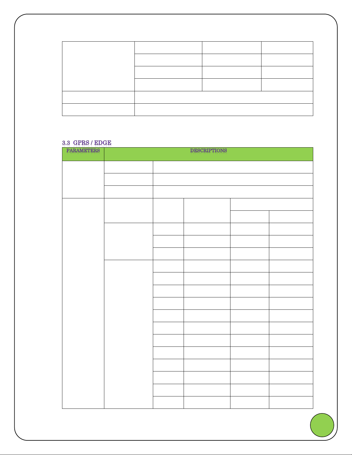
Spectrum Emission Mask
Below -35 dBc
2.5 – 3.5 MHz
Offset 30KHz
Below -35 dBc
3.5 – 7.5 MHz
Offset 1MHz
Below -39 dBc
7.5 – 8.5 MHz
Offset 1MHz
Below -49 dBc
8.5 – 12.5 MHz
Offset 1MHz
Occupied Bandwidth
Below 5MHz
ACLR
±5MHz 33dB, ±10MHz 43dB
Frequency
Range
GPRS / EDGE 850
Up: 824 ~ 849 MHz
GPRS / EDGE 900
Up: 880 ~ 915 MHz
GPRS / EDGE 1800
Up: 1710 ~ 1785 MHz
Transmitter
output power
Band
Power
Level
Output Power
(dBm)
Tolerances
Normal
Extreme
GPRS 850/900
5
33
±2
±2.5
6
31
±3
±4
7
29
±2
±2.5
GPRS / EDGE / 850
/ 900
8
27
±3
±4
9
25
±3
±4
10
23
±3
±4
11
21
±3
±4
12
19
±3
±4
13
17
±3
±4
14
15
±3
±4
15
13
±3
±4
16
11
±5
±6
17 9 ±5
±6
18 7 ±5
±6
19 5 ±5
±6
Page 9
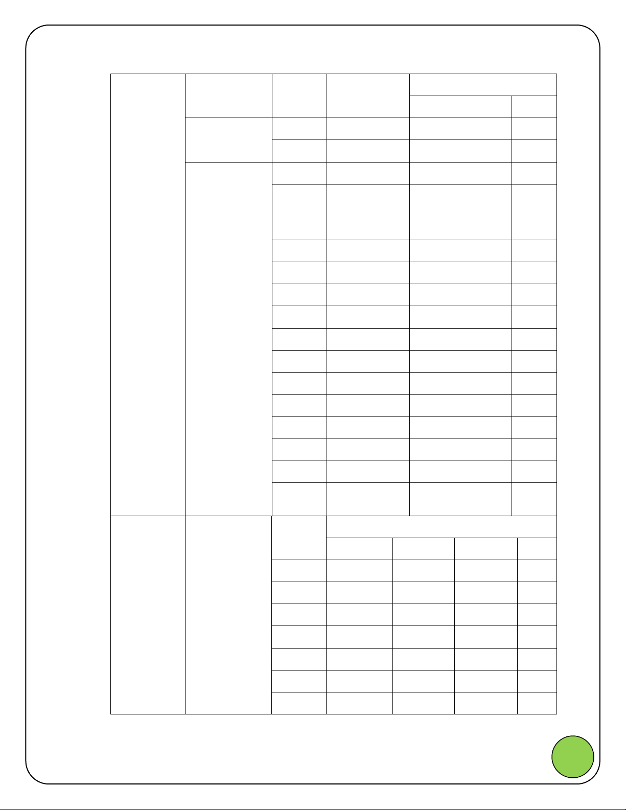
User Manual/ Specification September 22, 2013
8
User Manual/ Specification | 9/22/2013
Band
Power
Level
Output Power
(dBm)
Tolerances
Normal
Extreme
GPRS 1800
0
30
±2
±2.5
1
28
±3
±4
GPRS / EDGE /
1800
2
26
±3
±4
3
24
±2 (GPRS), ±3 (EDGE)
±2.5
(GPRS),
±4
(EDGE)
4
22
±3
±4
5
20
±3
±4
6
18
±3
±4
7
16
±3
±4
8
14
±3 (GPRS), ±4 (EDGE)
±4
9
12
±4
±5
10
10
±4
±5
11 8 ±4
±5
12 6 ±4
±5
13 4 ±4 (GPRS), ±5 (EDGE)
±5
14 2 ±5
±6
15 0 ±5 (GPRS)
±6
(GPRS)
ORFS @
Spectrum due to
modulation
GSM / GPRS 850 /
900
Power
(dBm)
Frequency offset (KHz)
±400
±600
±1200
±1800
33
-19
-21
-21
-24
31
-21
-23
-23
-26
29
-23
-25
-25
-28
27
-23
-26
-27
-30
25
-23
-26
-29
-32
23
-23
-26
-31
-34
≤20
-23
-26
-32
-36
Page 10
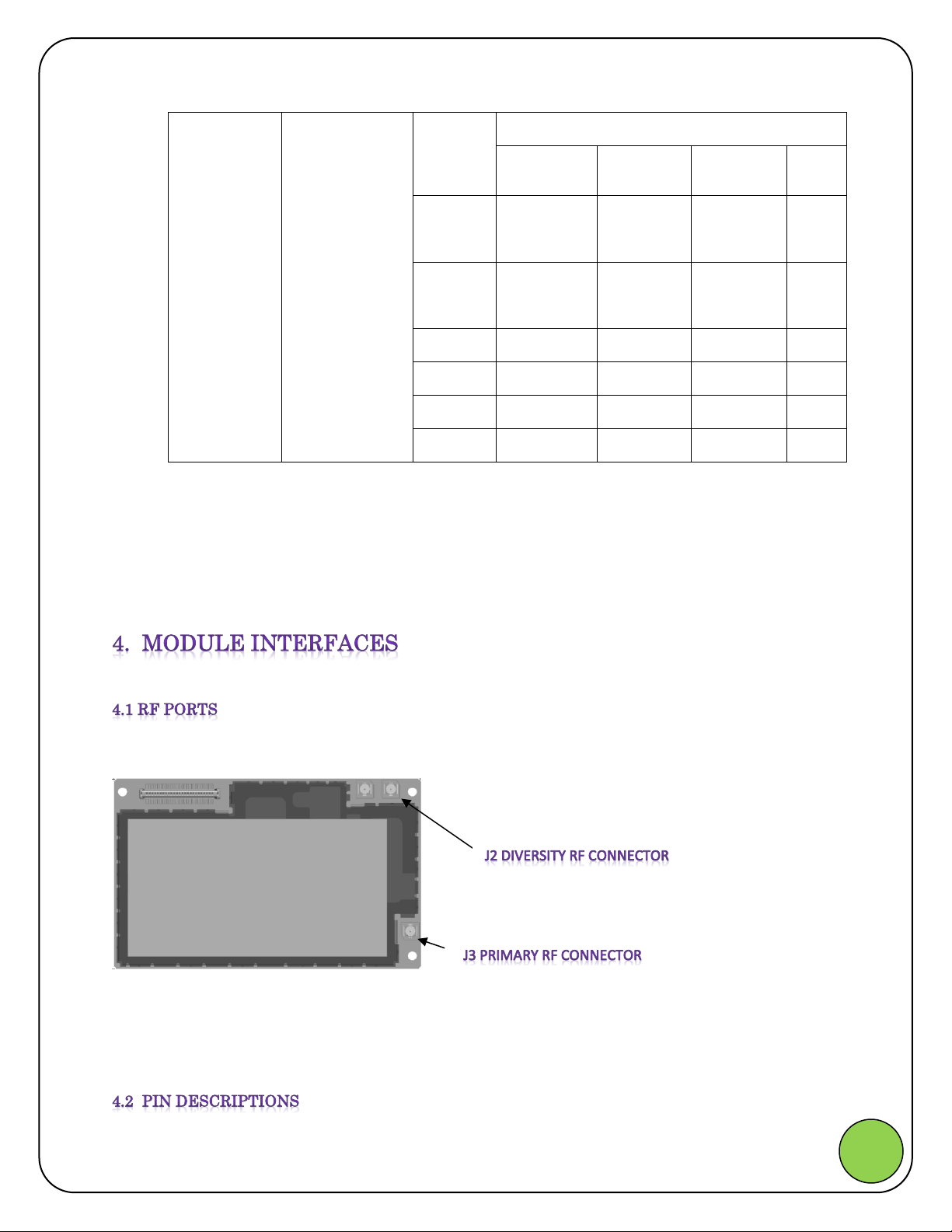
User Manual/ Specification September 22, 2013
9
User Manual/ Specification | 9/22/2013
ORFS @
Spectrum due to
switching
transient
GSM / GPRS 1800 /
1900
Power
(dBm)
Frequency offset (KHz)
±400
±600
±1200
±1800
30
-22
-24
-24
-27
28
-23
-25
-26
-29
26
-23
-26
-28
-31
24
-23
-26
-30
-33
22
-23
-26
-31
-35
≤20
-23
-26
-32
-36
Page 11
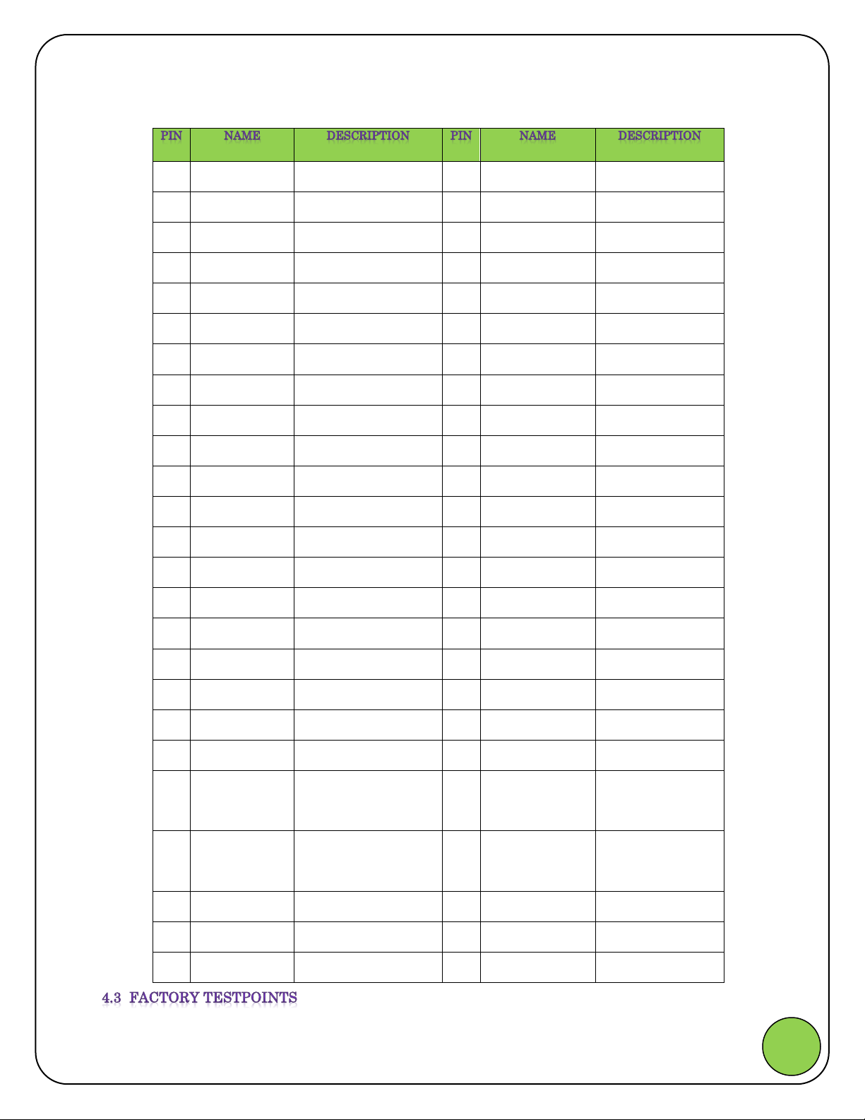
User Manual/ Specification September 22, 2013
10
User Manual/ Specification | 9/22/2013
1
GND
Ground
2
VBAT
Battery
3
GND
Ground
4
VBAT
Battery
5
GND
Ground
6
VBAT
Battery
7
GND
Ground
8
VBAT
Battery
9
GND
Ground
10
VBAT
Battery
11
GND
Ground
12
VBAT
Battery
13
GND
Ground
14
VBAT
Battery
15
GND
Ground
16
VBAT
Battery
17
GND
Ground
18
VBAT
Battery
19
RSVD
Reserved
20
RSVD
Reserved
21
PS_HOLD
Power Supply Hold Up
22
UART_RX_AP
Serial Receive
23
LTE_SYNC
LTE/B7 coexistence
24
UART_TX_AP
Serial Transmit
25
FW_RDY
Firmware Ready
26
JTAG_TDI
JTAG Data In
27
SIM_PRST_N
SIM card detect
28
JTAG_TDO
JTAG Data Out
29
GND
Ground
30
JTAG_TMS
JTAG Select
31
USB_DN
USB Data -
32
JTAG_TCK
JTAG Clock
33
USB_DP
USB Data +
34
JTAG_RTCK
JTAG Return Clock
35
GND
Ground
36
JTAG_TRST_N
JTAG Test Reset
37
USB_EN
USB Enable
38
JTAG_SRST_N
JTAG System Reset
39
HOSTWAKE
HOSTWAKE
40
WLAN_PRIORITY
LTE/B7 coexistence
41
I2C_CLK_HMI
Host to Modem Interrupt
I2C Clock
42
GSM_TX
GSM Blanking signal
43
I2C_DATA_HMI
Modem to Host Interrupt
I2C Data
44
UICC_DATA
SIM DATA
45
RESTIN_N
Hard Reset
46
UICC_CLK
SIM Clock
47
LTE_ACTIVE
LTE/B7 coexistence
48
UICC_RST
SIM Reset
49
PWR_ON_OFF
Modem ON/OFF
50
VREG_SIM_2P85
SIM Voltage
Page 12
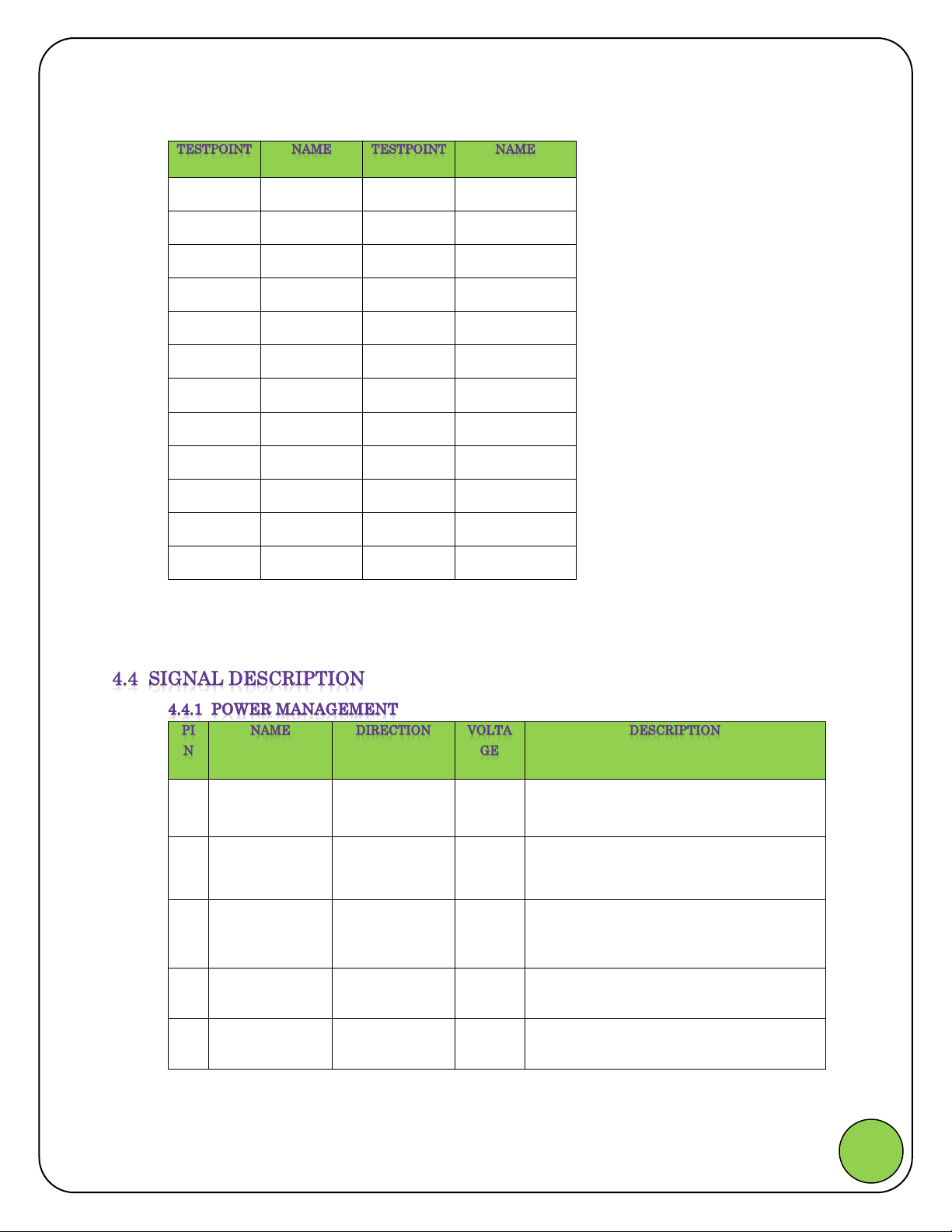
User Manual/ Specification September 22, 2013
11
User Manual/ Specification | 9/22/2013
TP1
VBAT
TP13
GND
TP2
VBAT
TP14
USB_DN
TP3
VBAT
TP15
USB_DP
TP4
VBAT
TP16
UICC_DATA
TP5
UART_RX_AP
TP17
RESETIN_N
TP6
UART_TX_AP
TP18
VREG_SIM_2P85
TP7
USB_EN
TP19
PWR_ON_OFF
TP8
UICC_CLK
TP20
PS_HOLD
TP9
UICC_RST
TP21
SIM_PRST_N
TP10
GND
TP11
GND
TP12
GND
21
PS_HOLD
Modem Host
1.8V
Connect to 1.8V(VREG_MSME) to enable JTAG
debug mode
49
PWR_ON_OFF
Host Modem
1.8V
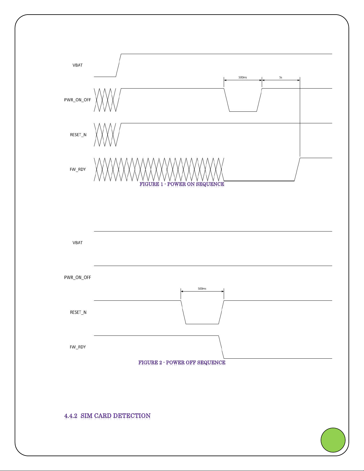
Pulling LOW for 500ms toggles power ON/OFF.
Must be driven open collector (has internal pull
up).
37
USB_EN
Host Modem
1.8V /
3.3V
Enable/Disable USB PHY. Enable only during
USB data transfer to minimize power
consumption.
45
RESETIN_N
Host Modem
1.8V
Active Low, Hard reset. Resets PMIC when
asserted.
25
FW_READY
Modem Host
1.8V
Pin goes HIGH when the module has competed
boot sequence.
Page 13
User Manual/ Specification September 22, 2013
12
User Manual/ Specification | 9/22/2013
Page 14
User Manual/ Specification September 22, 2013
13
User Manual/ Specification | 9/22/2013
23
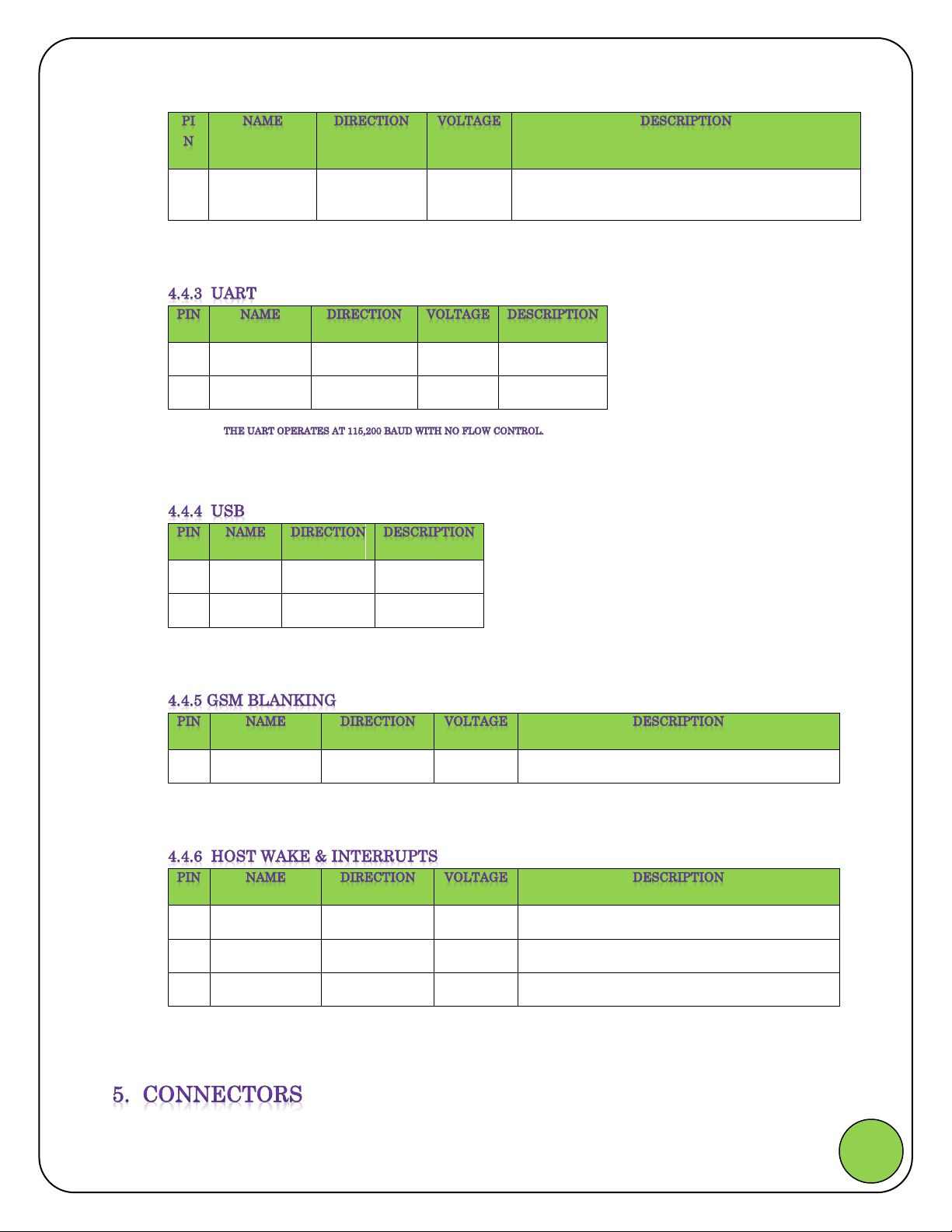
SIM_PRST_N
Host -> Modem
1.8V
Host Device MCU pulls this signal to high when SIM
card is present. Low when the SIM card is absent.
22
UART_RX_AP
Host Modem
1.8V
Receive Data
24
UART_TX_AP
Modem Host
1.8V
Transmit Data
31
USB_DM
Bidirectional
USB Data -
33
USB_DP
Bidirectional
USB Data +
42
GSM_TX
Modem Host
1.8V
Logic High during GSM transmits.
41
HMI
Host Modem
1.8V
Host to Modem Interrupt
43
MHI
Modem Host
1.8V
Modem to Host Interrupt
39
HOSTWAKE
Modem Host
1.8V
Modem wake Host signal
Page 15
User Manual/ Specification September 22, 2013
14
User Manual/ Specification | 9/22/2013
Page 16
User Manual/ Specification September 22, 2013
15
User Manual/ Specification | 9/22/2013
Page 17
User Manual/ Specification September 22, 2013
16
User Manual/ Specification | 9/22/2013
Page 18
User Manual/ Specification September 22, 2013
17
User Manual/ Specification | 9/22/2013
This device complies with part 15 of the FCC Rules. Operation is subject to the following two
conditions: (1) This device may not cause harmful interference, and (2) this device must accept any
interference received, including interference that may cause undesired operation.
This device has been tested and found to comply with the limits for a Class B digital device,
pursuant to Part 15 of the FCC Rules. These limits are designed to provide reasonable protection
against harmful interference in a residential installation. This equipment generates, uses and can
radiated radio frequency energy and, if not installed and used in accordance with the instructions, may
cause harmful interference to radio communications. However, there is no guarantee that interference
will not occur in a particular installation if this equipment does cause harmful interference to radio or
television reception, which can be determined by turning the equipment off and on, the user is
encouraged to try to correct the interference by one or more of the following measures:
-Reorient or relocate the receiving antenna.
-Increase the separation between the equipment and receiver.
-Connect the equipment into an outlet on a circuit different from that to which the receiver is
connected.
-Consult the dealer or an experienced radio/TV technician for help.
Changes or modifications not expressly approved by the party responsible for compliance
could void the user‘s authority to operate the equipment.
The antenna(s) used for this transmitter must not be co-located or operating in conjunction with
any other antenna or transmitter.
Changes or modifications not expressly approved by the party responsible for compliance could
void the user‘s authority to operate the equipment.
This device meets the government’s requirements for exposure to radio waves.
This device is designed and manufactured not to exceed the emission limits for exposure to radio
frequency (RF) energy set by the Federal Communications Commission of the U.S. Government.
This device complies with FCC radiation exposure limits set forth for an uncontrolled environment.
In order to avoid the possibility of exceeding the FCC radio frequency exposure limits, human
proximity to the antenna shall not be less than 20cm (8 inches) during normal operation.
Maximum antenna gain allowed for use with this device is +2 dBi.
When the module is installed in the host device, the FCC ID label must be visible through a window
on the final device or it must be visible when an access panel, door or cover is easily re-moved. If not,
a second label must be placed on the outside of the final device that contains the following text:
This device is intended only for OEM integrators under the following conditions:
1) The antenna must be installed such that 20 cm is maintained between the antenna and
users, and
Page 19
User Manual/ Specification September 22, 2013
18
User Manual/ Specification | 9/22/2013
1) The antenna must be installed such that 20 cm is maintained between the
antenna and users, and
2) The transmitter module may not be co-located with any other transmitter
or antenna. As long as 2 conditions above are met, further transmitter test
will not be required.
However, the OEM integrator is still responsible for testing their end-product
for any additional compliance requirements required with this module
installed
In the event that these conditions cannot be met (for example certain laptop
configurations or co -location with another transmitter), then the FCC authorization
is no longer considered valid and the FCC ID cannot be used on the final product. In
these circumstances, the OEM integrator will be responsible for re-evaluating the
end product (including the transmitter) and obtaining a separate FCC authorization.
This transmitter module is authorized only for use in device where the antenna may
be installed such that 20 cm may be maintained between the antenna and users.
The final end product must be labeled in a visible area with the following: “Contains
FCC ID: RM4-CO3L”. The grantee's FCC ID can be used only when all FCC
compliance requirements are met.
The OEM integrator has to be aware not to provide information to the end user
regarding how to install or remove this RF module in the user’s manual of the end
product which integrates this module.
The end user manual shall include all required regulatory information/warning as
show in this manual.
 Loading...