

Page 1

CORELIS
PCIe-1149.1
PCIe-1149.1
High-Speed PCI Express Bus
Boundary-Scan Controller
User’s Manual
Document Part Number: 70369 REV B
Copyright 2006 - 2007 Corelis Inc.
12607 Hidden Creek Way
Cerritos, CA 90703-2146
Telephone: (562) 926-6727 • Fax: (562) 404-6196
Page 2

Page 3

Preface
PRINTING HISTORY
New editions are complete revisions of the manual. Update packages, which are issued between
editions, contain additional and replacement pages to be merged into the manual by the customer.
The dates on the title page change only when a new edition is published.
A software code may be printed before the date; this indicates the version of the software product at
the time the manual or update was issued. Many product updates and fixes do not require manual
changes and, conversely, manual corrections may be done without accompanying product changes.
Therefore, do not expect a one to one correspondence between product updates and manual
updates.
Revision A, September 2006
Revision B, November 2007
GENERAL NOTICE
Information contained in this document is subject to change without notice. CORELIS shall not be
liable for errors contained herein for incidental or consequential damages in connection with the
furnishing, performance, or use of material contained in this manual. This document contains
proprietary information, which is protected by copyright. All rights reserved. No part of this
document may be reproduced or translated to other languages without the prior written consent of
CORELIS.
CORELIS assumes no responsibility for the use of or reliability of its software on equipment that is
not furnished by CORELIS.
ENVIRONMENTAL NOTICE
This product must be disposed of in accordance with the WEEE directive.
TRADEMARK NOTICE
Windows is a registered trademark of Microsoft Corporation.
Other products and services named in this book are trademarks or registered trademarks of their
respective companies. All trademarks and registered trademarks in this book are the property of
their respective holders.
i
Page 4

PRODUCT WARRANTY
This CORELIS product has a warranty against defects in material and workmanship for a period of
90 days from date of shipment. During the warranty period, CORELIS will, at its option, either
repair or replace products that prove to be defective.
For warranty service or repair, this product must be returned to a service facility designated by
CORELIS. Outside CORELIS service travel areas, warranty service will be performed at the
Buyer's facility only upon CORELIS' prior agreement and Buyer shall pay CORELIS' round trip
travel expenses.
For products returned to CORELIS for warranty service, the Buyer shall prepay shipping charges to
CORELIS and CORELIS shall pay shipping charges to return the product to the Buyer. However,
the Buyer shall pay all shipping charges, duties, and taxes for products returned to CORELIS from
another country.
CORELIS warrants that its software and firmware designated by CORELIS for use with an
instrument will execute its programming instructions when properly installed on that instrument.
CORELIS does not warrant that the operation of the instrument, software, or firmware will be
uninterrupted or error-free.
The foregoing warranty shall not apply to defects resulting from improper or inadequate
maintenance by the Buyer, Buyer-supplied software or interfacing, unauthorized modification or
misuse, operation outside of the environmental specifications for the product, or improper site
preparation or maintenance.
NO OTHER WARRANTY IS EXPRESSED OR IMPLIED. CORELIS SPECIFICALLY
DISCLAIMS THE IMPLIED WARRANTIES OF MERCHANTABILITY AND FITNESS FOR
A PARTICULAR PURPOSE.
EXCLUSIVE REMEDIES
THE REMEDIES CONTAINED HEREIN ARE THE CUSTOMER'S SOLE AND
EXCLUSIVE REMEDIES. CORELIS SHALL NOT BE LIABLE FOR ANY DIRECT,
INDIRECT, SPECIAL, INCIDENTAL, OR CONSEQUENTIAL DAMAGES, WHETHER
BASED ON CONTRACT, TORT, OR ANY OTHER LEGAL THEORY.
Product maintenance agreements and other customer assistance agreements are available for Corelis
products. For assistance, contact your nearest Corelis Sales and Service Office.
RETURN POLICY
No items returned to CORELIS for warranty, service, or any other reason shall be accepted unless
first authorized by CORELIS, either direct or through its authorized sales representatives. All
returned items must be shipped pre-paid and clearly display a Returned Merchandise Authorization
(RMA) number on the shipping carton. Freight collect items will NOT be accepted. Customers or
authorized sales representatives must first contact CORELIS with notice of request for return of
merchandise. RMA's can only originate from CORELIS. If authorization is granted, an RMA
number will be forwarded to the customer either directly or through its authorized sales
representative.
ii
Page 5

Table of Contents
CHAPTER 1 PRODUCT OVERVIEW..........................................................................1-1
Introduction................................................................................................................................................1-1
What Is IEEE Standard 1149.1? ................................................................................................................1-2
Features of the PCIe-1149.1 ......................................................................................................................1-3
Adjustable Voltage Interfaces................................................................................................................................ 1-4
Parallel Input/Output Ports.................................................................................................................................... 1-4
PCI Express Interface............................................................................................................................................1-4
Programmable Clocks............................................................................................................................................1-5
Features of the ScanTAP-4........................................................................................................................1-5
PCIe-1149.1 Specifications........................................................................................................................1-6
ScanTAP-4 Specifications .........................................................................................................................1-7
CHAPTER 2 PCIE-1149.1 INSTALLATION ................................................................2-1
Software Installation First! ........................................................................................................................2-2
Hardware Installation.................................................................................................................................2-2
Hardware Installation.................................................................................................................................2-3
CHAPTER 3 CONNECTING TO THE TARGET..........................................................3-1
Connecting to the Target............................................................................................................................3-1
20-Pin ScanTAP Connector.......................................................................................................................3-3
68-pin Host Connector...............................................................................................................................3-4
PCIe-1149.1 Parallel I/O Connectors.........................................................................................................3-5
CHAPTER 4 USING PCIE-1149.1 WITH SCANPLUS ................................................4-1
Hardware Setup..........................................................................................................................................4-1
Using PCIe-1149.1 with ScanPlus Tools...................................................................................................4-1
ScanTAP-4 TAP Configuration.................................................................................................................4-5
TAP Configuration - Method 1..................................................................................................................4-6
TAP Configuration - Method 2..................................................................................................................4-8
TAP Configuration - Method 3..................................................................................................................4-9
Gang Programming with ScanPlus Runner .............................................................................................4-13
Gang Programming with ScanPlus Flash Programmer............................................................................4-20
CHAPTER 5 THIRD PARTY APPLICATION INTERFACE.........................................5-1
Using PCIe-1149.1 with ScanPlus Runner Command-line.......................................................................5-1
APPENDIX A RECOMMENDED TARGET CONNECTORS ..........................................1
10-pin TAP Connector..................................................................................................................................1
Flash Programming TAP Connector.............................................................................................................4
20-pin TAP Connector..................................................................................................................................7
iii
Page 6

APPENDIX B SELF TEST UTILITY SOFTWARE.......................................................... 1
Self-Test........................................................................................................................................................1
iv
Page 7

Table of Figures
Figure 1-1. The Corelis PCIe-1149.1 Boundary-Scan Controller ........................................................................... 1-1
Figure 1-2. Test Access Port (TAP).......................................................................................................................... 1-2
Figure 1-3. PCIe-1149.1 Block Diagram................................................................................................................. 1-3
Figure 3-1. ScanTAP-4 20-pin TAP Header Connectors (top view)........................................................................ 3-1
Figure 4-1. Controller Configuration Screen........................................................................................................... 4-1
Figure 4-2. PCIe-1149.1 Setup Screen (but ScanTAP-4 not connected).................................................................. 4-2
Figure 4-3. Successful PCIe-1149.1 With ScanTAP Setup Screen........................................................................... 4-3
Figure 4-4. Advanced Configuration Setup Screen.................................................................................................. 4-4
Figure 4-5. Controller Configuration TAP Configuration Options..........................................................................4-6
Figure 4-6. Typical ScanPlus Runner Test Plan...................................................................................................... 4-9
Figure 4-7. ScanPlus Runner Pop-up Menu........................................................................................................... 4-10
Figure 4-8. Infrastructure Test Options Dialog Box.............................................................................................. 4-11
Figure 4-9. Available ScanTAP-4 Configuration................................................................................................... 4-12
Figure 4-10. ScanPlus Runner Test Plan for Gang Programming......................................................................... 4-14
Figure 4-11. ScanPlus Runner Pop-up Menu......................................................................................................... 4-15
Figure 4-12. Infrastructure Test Options Dialog Box............................................................................................ 4-16
Figure 4-13. Available ScanTAP-4 TAP Configuration......................................................................................... 4-17
Figure 4-14. Available ScanTAP-4 TAP Configuration for .fpi files...................................................................... 4-18
Figure 4-15. ScanPlus Flash Programmer Gang Programming Window..............................................................4-20
Figure A-1. Standard TAP connector (top view)..........................................................................................................1
Figure A-2. TAP Connector Schematic........................................................................................................................3
Figure A-3. Boundary-scan Flash Programming 16 Pin TAP Connector (top view)...................................................4
Figure A-4. Flash Programming TAP Connector Schematics......................................................................................6
Figure A-5. Boundary-scan Flash Programming 20-Pin TAP Connector (top view)..................................................7
Figure A-6. 20-pin TAP Connector Schematic for SPI................................................................................................10
Figure A-7. 20-pin TAP Connector Schematic for I2C...............................................................................................11
Figure B-1. Self-Test Result for the PCIe-1149.1 when the ScanTAP-4 is NOT connected.........................................2
Figure B-2. Self-Test Results for the PCIe-1149.1 with the ScanTAP-4 Connected.....................................................3
v
Page 8

Table of Tables
Table 1-1. Programmable TCK Frequencies............................................................................................................ 1-5
Table 1-2. ScanTAP-4 DC Characteristics............................................................................................................... 1-7
Table 1-3. ScanTAP-4 SPI Interface DC Characteristics.........................................................................................1-8
Table 1-4. ScanTAP-4 I2C Interface DC Characteristics........................................................................................ 1-9
Table 3-1. ScanTAP-4 TAP Pin Assignment............................................................................................................. 3-3
Table 3-2. 68-Pin SCSI type Cable Parts................................................................................................................. 3-4
Table 3-3. Connector P2 Parallel Output Pin Assignment.......................................................................................3-5
Table 3-4. Connector P1 Parallel Input Pin Assignment......................................................................................... 3-6
Table 4-1. ScanPlus Runner ScanTAP-4 Configuration........................................................................................... 4-7
Table 4-2. ScanPlus Runner Naming Conventions.................................................................................................... 4-8
Table 4-3. ScanPlus Runner Naming Conventions for Gang Programming........................................................... 4-13
Table 4-4. ScanPlus Runner ScanTAP-4 Configuration......................................................................................... 4-19
Table 5-1. PCIe-1149.1 Controller Parameters....................................................................................................... 5-2
Table A-1. Signal Description and Termina t i on...........................................................................................................2
Table A-2. Standard 10-Pin TAP Connector ................................................................................................................2
Table A-3. Flash Programming TAP 16 Pin Connector...............................................................................................5
Table A-4. Signal Description and Termina t i on...........................................................................................................5
Table A-5. Flash Programming TAP 16 Pin Connector...............................................................................................8
Table A-6. Signal Description and Termina t i on...........................................................................................................9
vi
Page 9

Chapter 1
Product Overview
Introduction
The PCIe-1149.1 High-Speed PCI Express Bus boundary-scan controller is a member of the Corelis
ScanExpress™ family of high performance scan-based test, analysis, and diagnostic tools. The
PCIe-1149.1 High-Speed PCI Express (PCIe) Bus Boundary-Scan Controller card, with memorybehind-the-pin architecture, interfaces between a host computer and any IEEE Standard 1149.1
compatible target. The PCIe-1149.1 is designed to control the operation of an IEEE Standard
1149.1 boundary-scan test path by generating the proper signals under software control to interface
with the target system. It also supports remote operation of multiple boundary-scan (JTAG) Test
Access Ports (TAPs) using any of the Corelis ScanTAP family of Multiple TAP Intelligent pods such
as the ScanTAP-4, ScanTAP-8 or ScanTAP-32. The PCIe-1149.1 is shown in Figure 1-1.
Figure 1-1. The Corelis PCIe-1149.1 Boundary-Scan Controller
The most popular Intelligent Pod is the ScanTAP-4. It connected to the PCIe-1149.1 card via a
standard SCSI-II cable and it provides up to 4 independent TAP connectors with a programmable
low-voltage-compatible interface. Each of the 4 TAP connectors contains direct access to JTAG,
I2C and SPI interfaces. It also supports simultaneous programming and verification of Flash
memory devices at continuous scan clock (TCK) speeds of up to 80 MHz. The ScanTAP pods
include direct hardware compare of expected scan results and are therefore especially suitable for
gang (parallel) testing and programming of units under test (UUTs).
Product Overview 1-1
Page 10
The PCIe-1149.1 facilitates software-controlled boundary-scan operations per IEEE Standard
1149.1. It provides command access to the target’s Test Access Port (TAP), to verify PCB
interconnects, perform functional testing, and debug without manual probing. Furthermore, the
JTAG interface gives access to internal device functions that are not accessible via external probing,
enabling fault isolation within the device itself. The JTAG interface also enables programming
target Flash and CPLD devices, as well as downloading and uploading of data blocks to and from
various storage devices. Application software for the PCIe-1149.1 is sold separately.
What Is IEEE Standard 1149.1?
The IEEE Standard 1149.1 test bus and boundary-scan architecture enable control of an IC, board,
or system, via a standard four-signal interface. Each IEEE Standard 1149.1-compliant IC
incorporates a feature known as boundary-scan, which ensures that a JTAG controller can control
and observe each functional pin of the IC via the four-wire interface. A controller can load test,
debug, or initialization patterns serially into the appropriate IC(s) via the IEEE Standard 1149.1 test
bus. Thus, even with limited physical access, a user can observe or control IC, board, or system
functions.
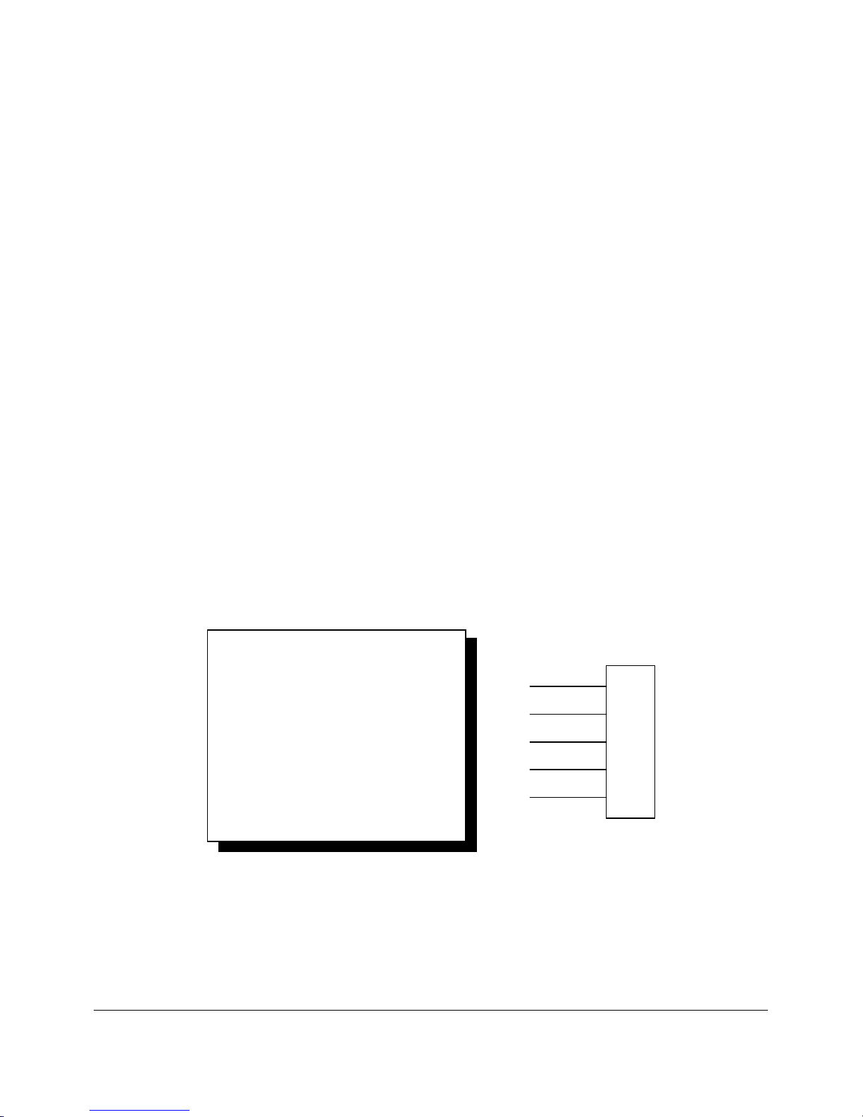
Two main elements comprise the IEEE Standard 1149.1 test bus: a Test Access Port (TAP), which
interfaces internal IC logic with the external world via a four-signal (optionally five-signal) bus as
shown in Figure 1-2, and a boundary-scan architecture, which defines standard boundary cells that
drive and receive data at the IC pins. IEEE Standard 1149.1 also defines both mandatory and
optional opcodes and test features. The test bus signals are: Test Clock (TCK), Test Mode Select
(TMS), Test Data In (TDI), Test Data Out (TDO), and the optional Test Logic Reset (TRST).
The IEEE-1149.1 Test Access Port
Interface (TAP) consists of four
required signals:
Test Mode Select (TMS)
Test Clock (TCK)
Test Data In (TDI)
Test Data Out (TDO)
A fifth signal is defined as optional:
Test Reset (TRST*)
TMS
TCK
TDI
TDO
TRST*
T
A
P
Figure 1-2. Test Access Port (TAP)
1-2 Product Overview
Page 11
Features of the PCIe-1149.1
The Corelis PCIe-1149.1 is a high performance JTAG controller that can access devices, boards or
systems compliant with IEEE Standard 1149.1. This PCI Express bus compatible card directly
supports one JTAG boundary-scan chain (TAP), expandable to additional TAPs using ScanTAP
intelligent pods. Two general purpose 8-bit parallel I/O ports are also provided for test and/or
control of non-boundary-scan areas of the unit under test (UUT). With its software-controlled
voltage translating logic, the PCIe-1149.1 can test low voltage systems. The SCSII type connector
includes high high-speed differential signals for reliable interfacing to external ScanTAP pods and it
supports high speed gang (parallel) testing and programming of multiple UUTs.
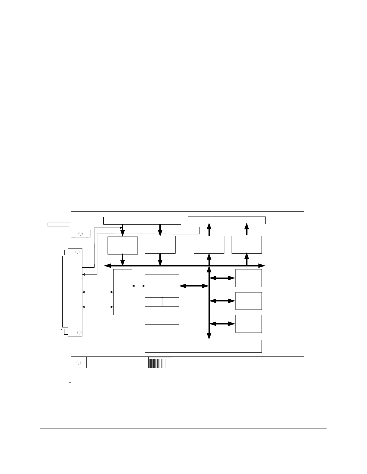
The PCIe-1149.1 contains several performance enhancing functional sections aimed at increasing
test vector throughput. A functional block diagram of the PCIe-1149.1 is shown in Figure 1-3. Key
functional elements include the TAP controller, and the memory resources that support it. The onboard memory provides scan data storage and can store the entire scan data for maximum
performance, real-time scan operations.
A test system accesses the TAP controller and its associated memory through the host PCI Express
bus memory-mapped I/O. This supports the high data rate of the PCI Express bus, regardless of
actual test clock speeds. The ability to download information into these memory elements further
decouples the scan operations from the host software. A state machine that contains status and
control registers accessible through the PCI Express bus controls all functions of the PCIe-1149.1.
68 Pin SCSI II type
Connector
ScanTAP
TAP
Interface
Remote
Pod I/F
Parallel Ports Input Connector
PORT A
Low Voltage
INPUTS
TAP ADJUSTABLE
VOLTAGE INTERFACE
PORT B
Low Voltage
INPUTS
TAP
CONTROLLER
Programmable
CLOCK
GENERATOR
Figure 1-3. PCIe-1149.1 Block Diagram
Parallel Ports Output Connector
PORT A
Low Voltage
OUTPUTS
J
PCI EXPRESS INTERFACE
PORT B
Low Voltage
OUTPUTS
MEMORY
MEMORY
CONTROL/
STATUS
Registers
The PCIe-1149.1 TAP controller contains special autonomous hardware accelerator mechanisms to
greatly increase performance where scan patterns repeat numerous times. This applies to target
download/upload sequences conveying large data blocks. As a result, time consuming tasks such as
Product Overview 1-3
Page 12

flash programming and emulator data transfers are more efficient for a given clock rate. This
mechanism off-loads the host interaction requirements by generating repeated vectors internally,
using host pre-loaded memory information. After host initialization, this mode of operation results
in continuous and maximal scanning rates at all clock frequencies. The only exception occurs when
the target paces the sequence by indicating a non-ready completion of data transfer, requiring a rescan of the target’s status. When not in this special mode, the scan stream bursts at the programmed
TCK rate, as paced by the flow of vector bits from the host.
Another performance enhancement provides hardware expected-value verification of scanned-back
data at programmable chain positions. Thus, the target output stream is evaluated without host
intervention and accompanying process delays. This further supports the above autonomous
operation enabling the scanning sequence to loop and rescan until the desired feedback is supplied,
also without host intervention.
A programmable, time delay skew compensation mechanism supports the PCIe-1149.1’s high clock
rates. This accommodates the returned target scan stream delays due to signal travel time down and
up the cables. It can also adjust for a target’s on-board TCK-to-TDO response delay.
An auxiliary feature of the PCIe-1149.1 is the target power-shorted detector for two voltages sense
target interface pins. With the target un-powered, this mechanism effectively measures the
impedance of the target load for each of two possible connected voltages, determining if a short
exists (some unacceptably low impedance). If this impedance is less than about 1 ohm (about an 11
watt target or greater at 3.3V, for example), it is deemed shorted.
Adjustable Voltage Interfaces
The software-programmable voltage level of the parallel I/O and TAP interfaces can be set to any
voltage between 1.25 V and 3.30 V in increments of 0.05V minimum.
Parallel Input/Output Ports
The PCIe-1149.1 contains 16 parallel inputs and 16 parallel outputs. The board groups these digital
I/O into two 8-bit parallel input ports, and two 8-bit parallel output ports: Port A and Port B. The
host computer can access the output ports via the Corelis ScanPlus Runner software. The input
ports are for future use and are not currently available to the user.
The output ports are useful for providing discrete signals that control functions on the user target
system such as reset, power control, and disable/enable signals for operating non-boundary-scan
devices on target boards that include some non IEEE-1149.1 compliant components.
PCI Express Interface
The PCIe-1149.1 is a single lane (x1)
(x1, x4, x8, x16).
It is mapped to 132 MB of memory space of the host system as established during
system initialization.
PCI Express add-in card, compatible with all compliant PCIe slots
1-4 Product Overview
Page 13
Programmable Clocks
The PCIe-1149.1’s programmable TCK outputs to the IEEE Standard 1149.1 compatible target
system can generate a wide range of TCK frequencies with onboard TCK generation circuitry. A
programmable Phase Locked Loop (PLL) and counter dividers provide both a wide range and fine
selection resolution. See Table 1-1 for the set of programmable values.
TCK range (MHz) Rate Resolution (MHz)
25 to 80 1
12.5 to 25 0.5
6.25 to 12.5 0.25
5 to 6.25 0.125
2.5 to 5 0.10
1.25 to 2.5 0.05
0.62 to 1.25 0.025
0.39 to 0.62 0.0156
0.05 to 0.39 0.05
Table 1-1. Programmable TCK Frequencies
Features of the ScanTAP-4
The Corelis ScanTAP-4 Multiple TAP Intelligent pod connects to the PCIe-1149.1 boundary-scan
controller via the 68-pin SCSI II type HOST connector. No external power supply is required—the
PCIe-1149.1 card supplies it. Differential signal driving supports cables of up to 30 feet. Automatic
delay mechanisms compensate for transport delays through the cable. The four TAPs are
individually configurable for interface voltages from 1.25 to 3.3 V. On-board voltage translation
logic allows a host to chain these TAPs together, or to configure them for gang programming.
During gang programming each TAP drives the same data out to up to four targets, and
simultaneously programs and verifies them. Optional Slow Slew rate (Voltages limited to 1.8 V to
3.3 V for slow slew) is provided. Each TAP can detect power shorts to ground for up to 2 voltages
per TAP (with user-provided test software), allowing the ScanTAP-4 to detect potentially damaging
conditions before the target system(s) is powered up.
Refer to Chapter 4 for further explanation on how to configure the ScanTAP-4 when using
ScanPlus Runner or ScanExpress Runner software tools.
Product Overview 1-5
Page 14

PCIe-1149.1 Specifications
Host Computer
CPU Pentium III @ 1 GHz or better
Operating System Windows 2000 or XP
PCI Express Interface
Width Single Lane (x1)
Memory Space Size 132 MB
ScanTAP Interface
Maximum TCK frequency 80 MHz
TCK frequency steps 1.00 MHz increments between 25 and 80 MHz
TCK frequency steps (cont’d) 0.80 MHz increments between 12.5 and 25 MHz
TCK frequency steps (cont’d) 0.25 MHz increments (or less) below 12.5 MHz
Maximum scanning data length unlimited
Physical
Card Outline Dimensions (PCB) 3.875 ± 0.25 inches × 6.75 ± 0.25 inches
I/O Connectors
P3 - Boundary-scan Connector 68-pin SCSI II type (AMP P/N 787171-7 or equivalent)
P1 - Input Port Connector 34-pin header (3M part no. 2534-6002UB or equivalent)
P2 - Output Port Connector 34-pin header (3M part no. 2534-6002UB or equivalent)
Power Requirements (from host expansion bus)
3.3 V 1.5 Amps maximum
On-board Fuse (feeds power from PCIe-1149.1 to external pod)
1.5 Amp, SLO-BLO
Littelfuse part number 045401.5
Operating Environment
Temperature 0C to 55C
Relative Humidity 10% to 90%, non condensing
Storage Environment
Temperature -40C to 85C
1-6 Product Overview
Page 15
ScanTAP-4 Specifications
PCIe-1149.1 Interface
Host Connector 68-pin SCSI type (AMP part no. 787171-7 or equivalent)
Host Cable Length: 6 foot (standard) - Corelis P/N 15314
15 foot (optional) - Corelis P/N 15328
30 foot (optional) - Corelis P/N 15329
TAP Interface
Connectors Four 20-pin shrouded headers, 0.1 in. × 0.1 in. spacing
Number of TAPs 4
Maximum TCK frequency 80 MHz (Concurrent scanning at all TAPs occurs at up to the
full TCK rate capability of the PCIe-1149.1)
Maximum scanning data length unlimited
Programmable Interface Voltage 1.25 to 3.3 V in 0.05 V increments
Programmable TAPs 4, each TAP can have its own programmable voltage settings
Signals DC characteristics See Table 1-2
Symbol Test Conditions Limit Min Limit Max Units
VIH Vdd Adjust >= 2.5 V 2 Vdd + 0.5 V
Vdd Adjust < 2.50 V 0.65 × Vdd Vdd + 0.5 V
VIL Vdd Adjust >= 2.00 0.7 V
Vdd Adjust <= 2.0 0.35 × Vdd V
VOH I
VOL I
= -2 mA Vdd – 0.35 V
OH
= 2 mA
OL
0.45 V
Vdd =1.65 V
IOH Vdd = 1.65-1.95 V -4 mA
IOL Vdd = 1.65-1.95 V 4 mA
Note: Also refer to Low Voltage CMOS (LVC) family signal characteristics data available from TI.
Product Overview 1-7
Table 1-2. ScanTAP-4 DC Characteristics
Page 16
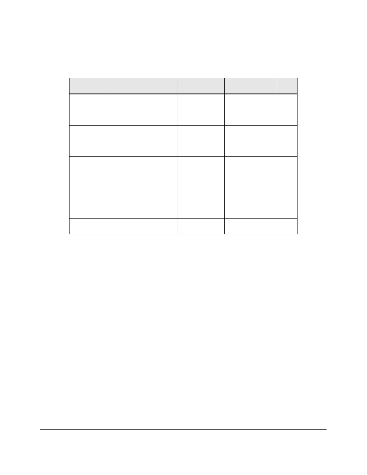
SPI Interface - available on ScanTAP-4 units P/N 10302A or later (with blue power-on LED)
SCK frequency 1 MHz
Signal DC Characteristics See Table 1-3:
Symbol Test Conditions Limit Min Limit Max Units
VIH Vdd Adjust >= 2.5 V 2 Vdd + 0.5 V
Vdd Adjust < 2.50 V 0.65 × Vdd Vdd + 0.5 V
VIL Vdd Adjust >= 2.00 0.7 V
Vdd Adjust <= 2.0 0.35 × Vdd V
VOH I
= -2 mA Vdd – 0.35 V
OH
IOL = 2 mA
VOL
0.45 V
Vdd =1.65 V
IOH Vdd = 1.65-1.95 V -4 mA
IOL Vdd = 1.65-1.95 V 4 mA
Table 1-3. ScanTAP-4 SPI Interface DC Characteristics
1-8 Product Overview
Page 17
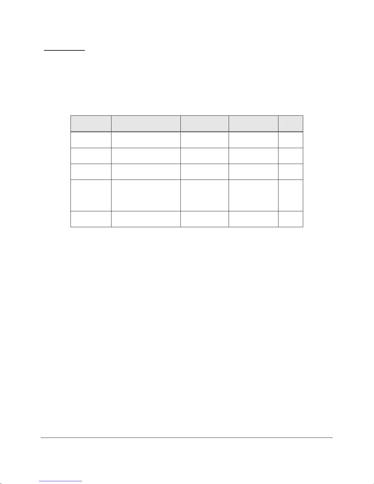
I2C Interface - available on ScanTAP-4 units P/N 10302A or later (with blue power-on LED)
The ScanTAP-4 I2C interface has open-drain outputs and the SDA/SCL signals must be pulled up
to 3.3V (VDD ) by the target.
SCL frequency 100 kHz
Signal DC Characteristics See Table 1-4:
Symbol Test Conditions Limit Min Limit Max Units
VDD 3.0 3.6 V
VIH V
VIL V
>= 3.3 V 2.0 3.6 V
DD
>= 3.3 V -0.5 0.8 V
DD
IOL = 16 mA
VOL
0.0 0.4 V
VDD = 3.3 V
IOL V
Table 1-4. ScanTAP-4 I2C Interface DC Characteristics
= 3.3 V 16 mA
DD
Product Overview 1-9
Page 18

Power Short Test Pins
Power (Vcc) Sense Pins 2 per TAP connector (Vcc1, Vcc2), 8 total
Vcc Measurement Type Short to GND detect, Target un-Powered,
Voltage sense/measurement of +/- 50 VDC
Voltage Sense Resolution 12-bit ADC
Voltage Sense Accuracy +/- 50 mV
Physical
Box Outline Dimensions 4.00 in. × 4.60 in. × 0.75 in.
Power Requirements
No external supply needed Power is provided by the host controller
Operating Environment
Temperature 0C to 55C
Relative Humidity 10% to 90%, non condensing
Storage Environment
Temperature -40C to 85C
1-10 Product Overview
Page 19

Chapter 2
PCIe-1149.1 Installation
The PCIe-1149.1 product typically consists of the following components:
PCIe-1149.1 PCI Express based boundary-scan controller card
PCIe-1149.1 User’s Manual
Ensure all materials listed are present and free from visible damage or defects before proceeding. If
anything appears to be missing or damaged, contact Corelis at the number listed on the front cover
immediately.
The ScanTAP-4 typically consists of the following components:
ScanTAP-4 box
Host Cable, 6-foot, 68-pin SCSI type, one-to-one Cable, Corelis P/N 15314
A set of four 20-pin to 10-pin TAP cables, Corelis P/N 15310
NOTE: The actual hardware shipped to the customer may vary depending on the customer order.
When this manual was published the following optional target interface TAP cables were available
from Corelis:
Bag of 4 TAP cables, 20-pin to 16-pin TAP, Corelis P/N 15311
Bag of 4 TAP cables, 20-pin to 20-pin TAP, Corelis P/N 15312
Special for RISCwatch / PowerPC, 20-pin to 16-pin TAP, Corelis P/N 15433
Special for MIPS, 20-pin to 14-pin TAP, Corelis P/N 15425
Host Cable, 15-foot, 68-pin SCSI type, one-to-one cable, Corelis P/N 15328
Host Cable, 30-foot, 68-pin SCSI type, one-to-one cable, Corelis P/N 15329
PCIe-1149.1 Installation 2-1
Page 20

Software Installation First!
The installation procedure requires the use of software that contains the driver for the PCIe-1149.1
card. Obtain the ScanPlus CD-ROM (or any other Corelis application that supports the PCIe-
1149.1 card) in order to proceed with installation. Install the ScanPlus Application Software
before installing the PCIe-1149.1 controller. The PCIe-1149.1 controller is a plug-and-play device,
and its drivers are installed with the ScanPlus Application Software. Windows will automatically
recognize and configure the PCIe-1149.1 the first time it is detected in your system.
WARNING !
You MUST install the software first – before installing the card. Do not install the PCIe-1149.1
card until you have successfully installed the application software (ScanPlus, CodeRunner,
etc.). Installing the software provides the plug-and-play driver for the card so that the operating
system is able to properly detect and configure the card. Installing the card before the software
may result in improper card configuration and operation.
2-2 PCIe-1149.1 Installation
Page 21

Hardware Installation
Again, make sure to install the ScanPlus Application Software before installing the PCIe-
1149.1 controller. The PCIe-1149.1 controller is a plug-and-play device, and its drivers are installed
with the ScanPlus Application Software. Windows will automatically recognize and configure the
PCIe-1149.1 the first time it is detected in your system.
To install the PCIe-1149.1 on a PC:
Update the PC BIOS and chipset drivers to the latest version from the manufacturer
Install ScanPlus Applications from the CD, and shut down the PC.
Remove the PCIe-1149.1 from its package.
Disconnect the PC power cord from the power source and then remove the enclosure
cover from the PC.
Plug the PCIe-1149.1 board into the PC in an available full height PCI Express slot.
Use a screw to firmly attach the PCIe-1149.1 card bracket to the PC chassis.
Close the PC enclosure, apply power and verify that the PC boots up correctly.
Preserve the original packing material for future shipment or storage of the PCIe-1149.1.
In the event that you installed the PCIe-1149.1 controller before installing the software, cancel the
Add/Remove Hardware Wizard and install the ScanPlus Applications from the CD. The next
time you start the PC, Windows will automatically recognize and configure the PCIe-1149.1.
Once the PCIe-1149.1 is installed in the PC, connect the ScanTAP-4 to the PCIe-1149.1 card using
the 68-pin SCSI type host cable:
Power down (shutdown) the PC
Plug the 68-pin host cable to the mating connector on the PCIe-1149.1 (that should not
protrude from the back of your PC enclosure).
Plug the other side of the 68-pin host cable to the HOST connector of the ScanTAP-4
box.
Apply power and verify that the PC boots up correctly. The “ON” LED should be
constantly illuminated when the PC is powered up.
PCIe-1149.1 Installation 2-3
Page 22

2-4 PCIe-1149.1 Installation
Page 23
Chapter 3
Connecting to the Target
Connecting to the Target
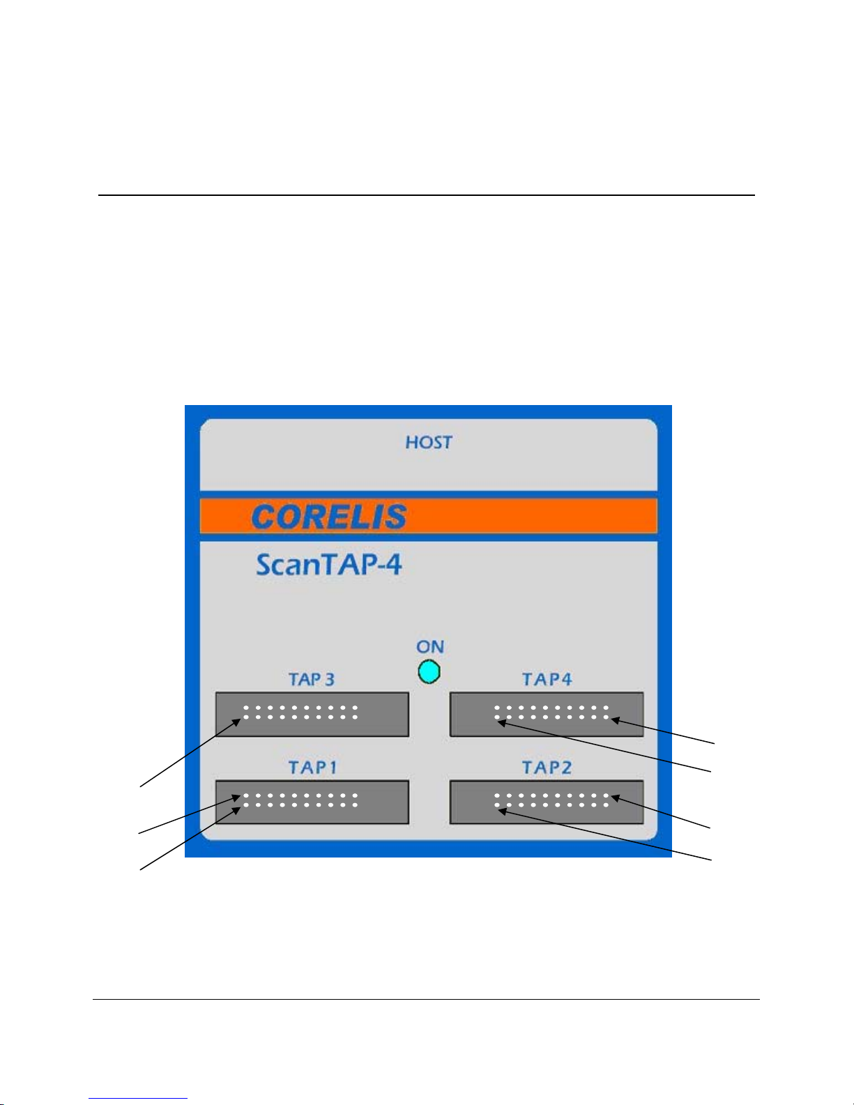
The connection to the user target (UUT) board/system is done from the ScanTAP-4 Intelligent Pod
TAP connectors to mating connectors on the target. The ScanTAP-4 connects to the target via the
supplied 1:1 TAP flat cables, P/N 15310, 15311 or 15312. Figure 3-1 shows the top view of the
ScanTAP-4 box, including the four TAP connectors which are clearly marked: TAP 1, TAP 2,
TAP 3 and TAP 4.
Pin 1
Pin 2
Pin 1
Figure 3-1. ScanTAP-4 20-pin TAP Header Connectors (top view)
Connecting to the Target 3-1
Pin 19
Pin 1
Pin 20
Pin 1
Page 24

While most targets use only a single TAP connector, it is not uncommon that targets contain
multiple TAP connectors. Although the 4-connector ScanTAP-4 will accommodate the vast
majority of multiple-TAP targets, a target board with more than 4 TAPs requires a different
interface. Please contact Corelis for other available products.
The following ScanTAP-4 TAP connectors are connected to the target board:
TAP1 - when the target has a single TAP connector
TAP1 and TAP2 - when the target has 2 TAP interface connectors
TAP1, TAP2 and TAP3 - when the target has 3 TAP interface connectors
TAP1, TAP2, TAP3 and TAP4 - when the target has 4 TAP interface connectors
To connect the TAP connector(s) to the target (UUT):
Make sure that the target power is OFF.
Make sure that the ON blue LED on top of the ScanTAP-4 is illuminated.
Install the TAP cable(s) on the ScanTAP-4 TAP connectors.
Install the other side of the TAP cable(s) on the matching target TAP connectors.
Now you can turn the target power ON.
Appendix A contains general recommendation for implementing compatible target TAP
connector(s). Following these recommendations makes the connection to the target easy and
straightforward. To accommodate target boards with TAP connectors other than this standard,
Corelis offers short, custom adapter cables for connectors such as the Altera ByteBlaster connector,
the Xilinx 9 pin header, the Lattice TAP connector or the TI 14 pin DSP connector)
3-2 Connecting to the Target
Page 25
20-Pin ScanTAP Connector
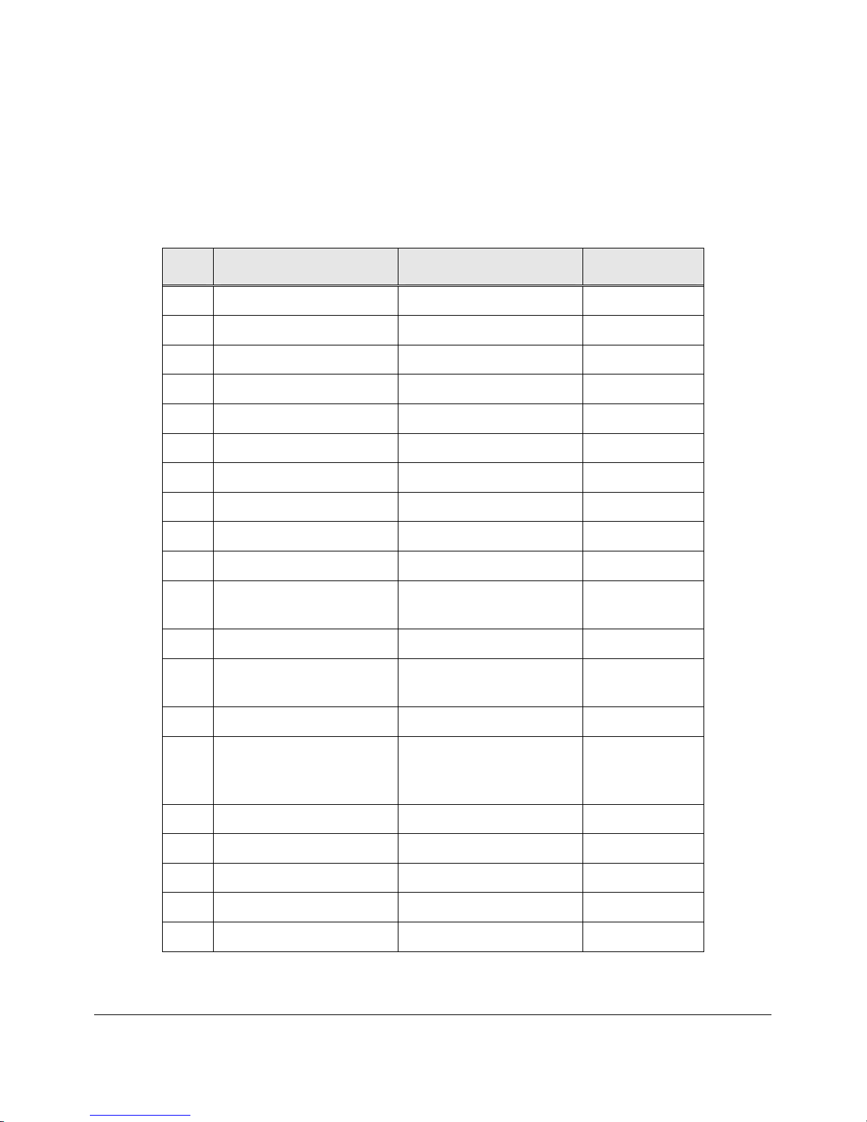
The ScanTAP-4 contains four 20-pin TAP connectors. All four connectors have the same signals
and the same pinout. Each connector is a shrouded header (0.100 × 0.100 in. spacing) with long
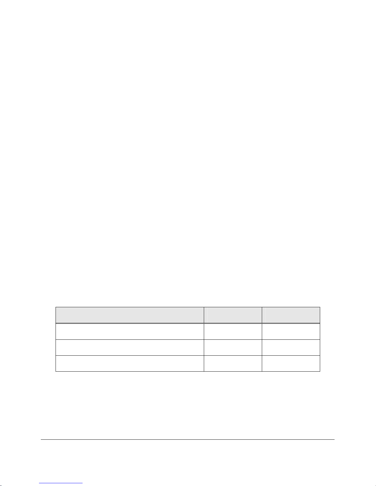
ejectors that are compatible with standard 20-pin IDC flat cable connectors (with strain relief). The
pin assignment is shown in Table 3-1.
Pin Signal Direction Termination
1 TRST* Input to the UUT 1K pull-up
2 GND
3 TDI Input to the UUT 1K pull-up
4 GND
5 TDO Output of the UUT 33 ohm series
6 GND
7 TMS Input to the UUT 1K pull-up
8 GND
9 TCK Input to the UUT 1K pull-up
10 GND
Write_Strobe* /
11
GPIO1 / SPI_CS2*
Input to the UUT 1K pull-up
12 GND
SPI_SCK /
13
GPIO2
Input to the UUT 1K pull-up
14 GND
Ready_Busy* /
15
SPI_SDO (MISO) /
Output of the UUT 1K pull-up
GPIO3
16 SPI_SDI (MOSI) Input to the UUT 1K pull-up
17 VCC1 UUT Power Test Point 1 None
18 I2C_SCL Input to the UUT 1K pull-up
19 VCC2 UUT Power Test Point 2 None
20 SPI_CS1* / I2C_SDA Input to the UUT 1K pull-up
Connecting to the Target 3-3
Table 3-1. ScanTAP-4 TAP Pin Assignment
Page 26
Note that only the first 10 pins are required. For Flash Programming with external write or the
Ready Busy signal, use the first 16 pins of the TAP. To build in support for power-to-ground short
checking, use all 20 pins of the TAP.
Pins 17 and 19 of each ScanTAP-4 connector can be used to sense that the target power pin is not
shorted to GND. Up to 2 different power pins can be checked on each of the four 20-pin
connectors of the ScanTAP-4 box.
The 3 GPIO signals are general purpose output signals that are directly controlled by the Parallel
I/O menu of ScanPlus Runner. Refer to the ScanPlus Runner manual for further information.
The dual purpose External Write* (GPIO1) signal is used for Flash programming, and if used will
override the Parallel Output (GPIO1) function. Refer to the ScanPlus Flash Programmer manual
for further information about this function.
The dual purpose Read/Busy* (GPIO3) signal is used for Flash programming, and if used will
override the Parallel Output (GPIO3) function. Refer to the ScanPlus Flash Programmer manual
for further information about this function.
The ScanTAP-4 comes standard with 4 short cables that connect it to a target system with up to 4
TAP connectors. These 20-pin to 10-pin cables, Corelis P/N 15310, are standard flat cables and can
easily be made from off-the-shelf connectors. Each cable mates with a matching 10-pin header on
the target system.
68-pin Host Connector
The PCIe-1149.1 connects to the ScanTAP-4 using a 68-wire, one-to-one, twisted-pair ribbon cable,
P/N 15314. Other HOST cables of longer lengths are also available.
Table 3-2 shows the part numbers for making custom length HOST flat cable. Note that this table
is provided for reference only and Corelis recommends using only approved HOST cables that are
provided with the product:
Description Manufacturer Part Number
68-pin .100 × .100 SCSI IDC Socket Circuit Assembly CA-68MDP-F
SCSI Strain Relief Circuit Assembly CA-LSR68MDP
0.25” Spectra-Strip twisted pair, 34-pair cable. Amphenol 125-3099-999
Table 3-2. 68-Pin SCSI type Cable Parts
3-4 Connecting to the Target
Page 27
PCIe-1149.1 Parallel I/O Connectors
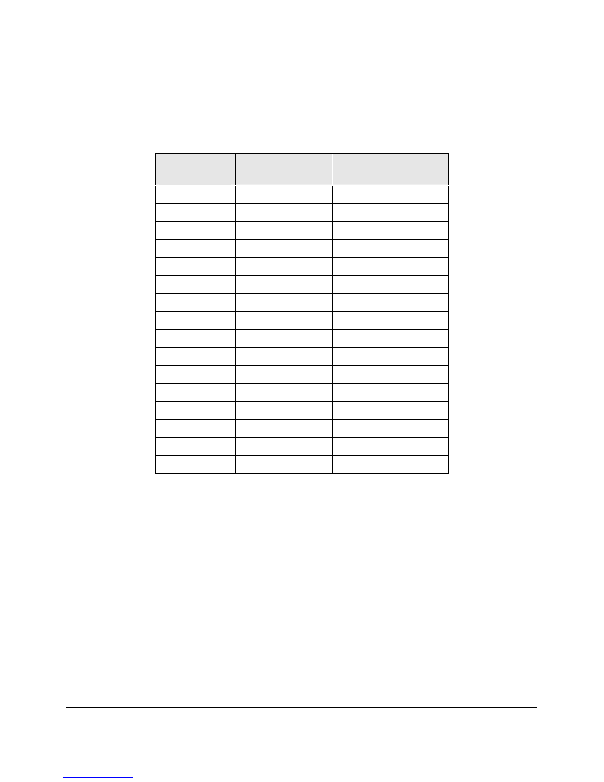
The parallel output port connector (P2 on the PCIe-1149.1) is a 34-pin connector that includes all of
the signals for the parallel output ports A and B. The connector is located near the top of the card.
The pin-out of the P2 connector is shown in Table 3-3.
Data Bus
Signal Name Output Connector
Alignment
D0 PORTA_OUT0 P2-1
D1 PORTA_OUT1 P2-3
D2 PORTA_OUT2 P2-5
D3 PORTA_OUT3 P2-7
D4 PORTA_OUT4 P2-9
D5 PORTA_OUT5 P2-11
D6 PORTA_OUT6 P2-13
D7 PORTA_OUT7 P2-15
D0 PORTB_OUT0 P2-17
D1 PORTB_OUT1 P2-19
D2 PORTB_OUT2 P2-21
D3 PORTB_OUT3 P2-23
D4 PORTB_OUT4 P2-25
D5 PORTB_OUT5 P2-27
D6 PORTB_OUT6 P2-29
D7 PORTB_OUT7 P2-31
Table 3-3. Connector P2 Parallel Output Pin Assignment
Note: All even pins of the connector (2, 4, 6, 8, …34) are connected to ground. P2-33 is not
connected.
Connecting to the Target 3-5
Page 28
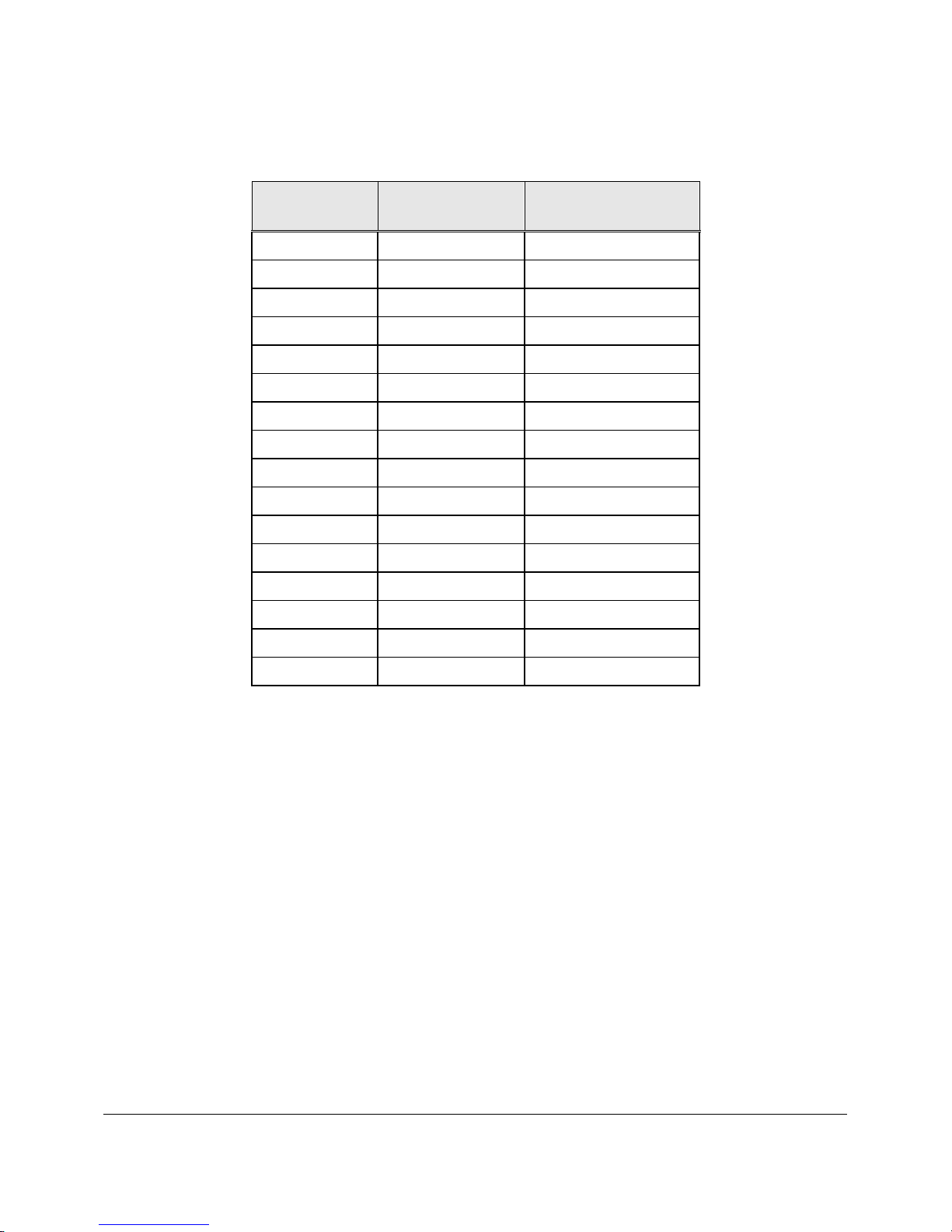
The parallel input port connector (P1 on the PCIe-1149.1) is a 34-pin connector that includes all of
the signals for the parallel input port. The connector is located near the top of the card. The pinout of the P1 connector is shown in Table 3-4.
Data Bus
Signal Name Input Connector
Alignment
D0 PORTA_IN0 P1-1
D1 PORTA_IN1 P1-3
D2 PORTA_IN2 P1-5
D3 PORTA_IN3 P1-7
D4 PORTA_IN4 P1-9
D5 PORTA_IN5 P1-11
D6 PORTA_IN6 P1-13
D7 PORTA_IN7 P1-15
D0 PORTB_IN0 P1-17
D1 PORTB_IN1 P1-19
D2 PORTB_IN2 P1-21
D3 PORTB_IN3 P1-23
D4 PORTB_IN4 P1-25
D5 PORTB_IN5 P1-27
D6 PORTB_IN6 P1-29
D7 PORTB_IN7 P1-31
Table 3-4. Connector P1 Parallel Input Pin Assignment
Note 1: All even pins of the connector (2, 4, 6, 8, …34) are connected to ground. P1-33 is not
connected.
Note 2: All input signals have a 4.7 K pull-up resistor to the programmed interface voltage (1.25
to 3.30 V). When the ScanTAP-4 is used, the 16 inputs and outputs interface at 3.3V.
3-6 Connecting to the Target
Page 29
Chapter 4
Using PCIe-1149.1 with ScanPlus
Hardware Setup
You must configure the PCIe-1149.1 controller in a ScanPlus application before the application can
use it. This chapter uses ScanPlus Runner as an example to illustrate the configuration process.
Using PCIe-1149.1 with ScanPlus Tools
The PCIe-1149.1 card is compatible with ScanPlus Runner, ScanPlus Debugger and ScanPlus Flash
Programmer. The following steps are provided for ScanPlus Runner. Selecting the card in ScanPlus
Debugger or ScanPlus Flash Programmer is done in a similar fashion.
1. Invoke the ScanPlus Runner application.
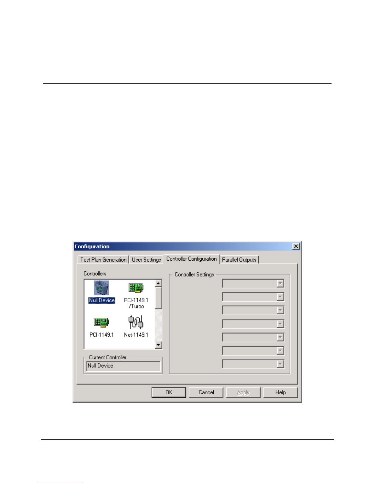
2. Click the Setup menu item and then select the Controller entry to display the Controller
Configuration screen shown in Figure 4-1.
Using PCIe-1149.1 with ScanPlus 4-1
Figure 4-1. Controller Configuration Screen
Page 30
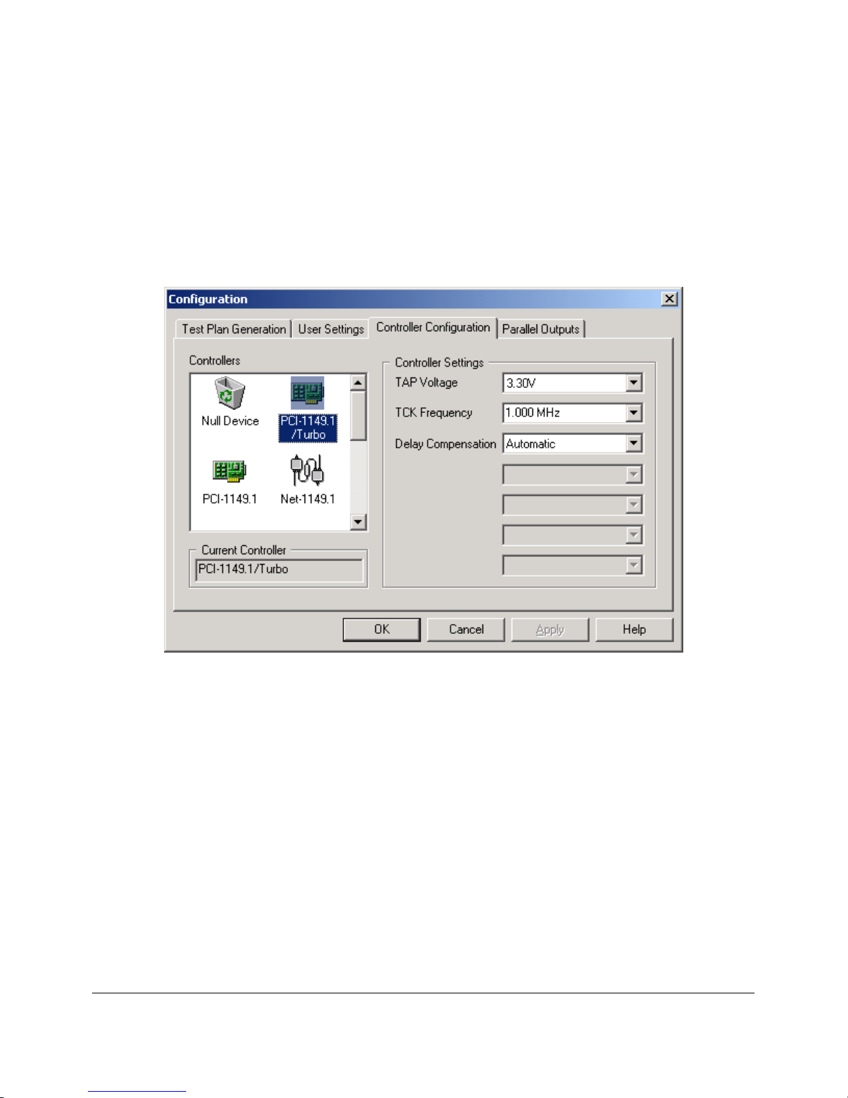
3. Select the PCIe-1149.1 controller from the icons on the left. Adjust the settings to the desired
values.
4. After you have made your selections, click on the Apply button to test and save the settings.
When the program saves the settings successfully, it displays the controller in the Current
Controller box. If ScanPlus Runner cannot find the controller, it displays an error dialog.
5. Once ScanPlus Runner finds the PCIe-1149.1 controller, if for some reason the ScanTAP-4 is
not connected to it, it displays a screen similar to Figure 4-2. If the ScanTAP-4 is connected
after seeing this screen you must exit this program and re-start at step 1.
Figure 4-2. PCIe-1149.1 Setup Screen (but ScanTAP-4 not connected)
4-2 Using PCIe-1149.1 with ScanPlus
Page 31
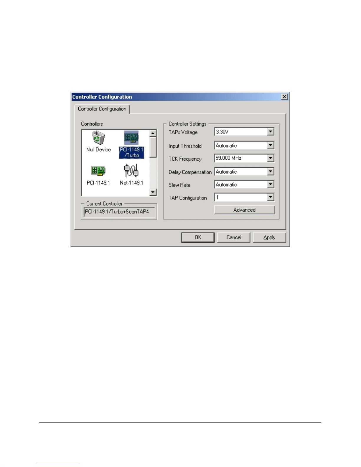
6. Once ScanPlus Runner finds the PCIe-1149.1 controller, with the ScanTAP-4 connected to it,
it displays a screen similar to Figure 4-3 Note that saving the test plan (.tsp) file in ScanPlus
Runner FILE menu also saves the settings in the system registry. The next time the .tsp file is
loaded into ScanPlus Runner it will use these settings to initialize the controller.
Figure 4-3. Successful PCIe-1149.1 With ScanTAP Setup Screen
Using PCIe-1149.1 with ScanPlus 4-3
Page 32
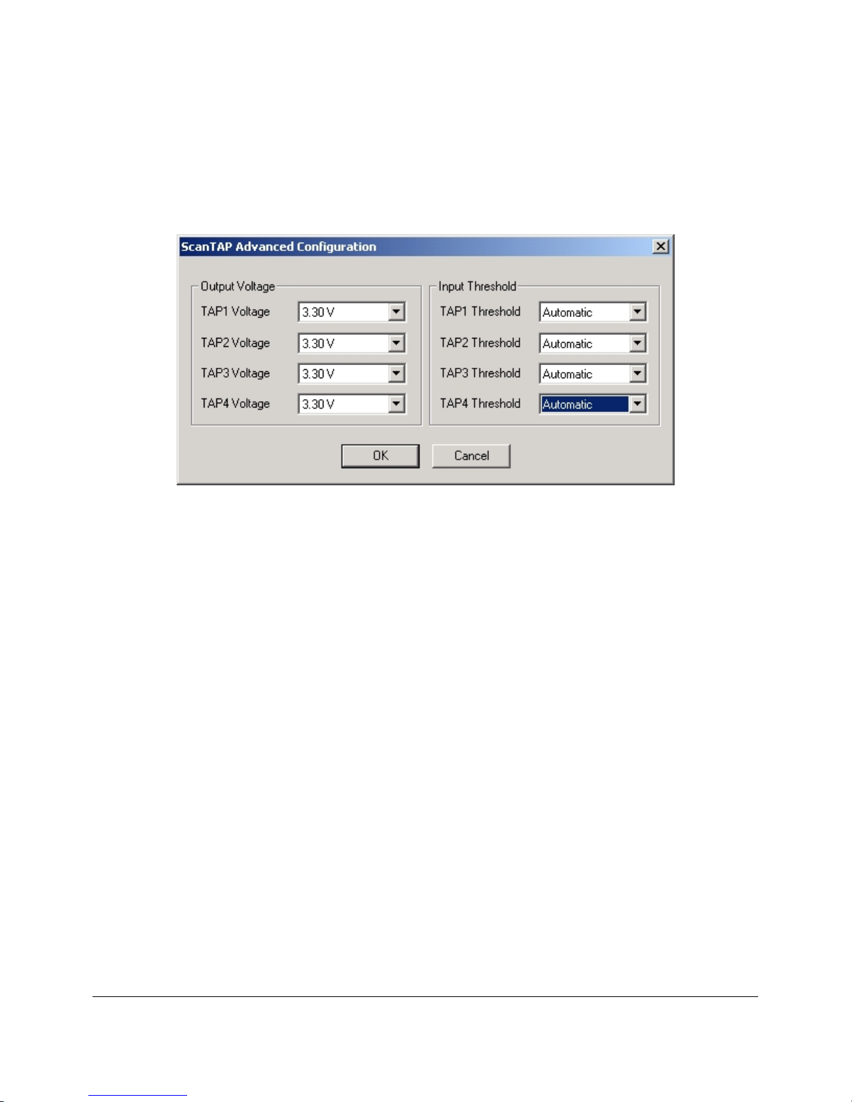
7. The Advanced button can be used for selecting different voltage settings for each individual
TAP. While most targets with multiple TAPs use the same voltage settings for all the TAPs it is
not uncommon to find targets that use, for example, the 3.3 V setting for one TAP, 2.5 V for
another, and 1.8 V for one or two additional TAPs. The Advanced Configuration screen is
shown in Figure 4-4.
Figure 4-4. Advanced Configuration Setup Screen
4-4 Using PCIe-1149.1 with ScanPlus
Page 33

ScanTAP-4 TAP Configuration
The ScanPlus Tools provide 3 different methods to specify the TAP(s) that connect the ScanTAP-4
to the target system:
Method 1 The TAP Configuration select box in the Controller Configuration screen (see
Figure 4-3). This is the preferred and most straightforward method for selecting
which of the 4 ScanTAP-4 TAPs to use for connecting to the target.
Method 2 Embedding the TAP selection text as part of the test step file name. This method is
explained below and is primarily supported for upwards compatibility with legacy
tools. This method is not recommended and will no longer be supported in future
software releases.
Method 3 Using the ScanPlus Runner tool Options menu. Use this method only when
specific test step(s) require TAP configuration settings different from the global
settings selected in Method 1 above.
Using PCIe-1149.1 with ScanPlus 4-5
Page 34
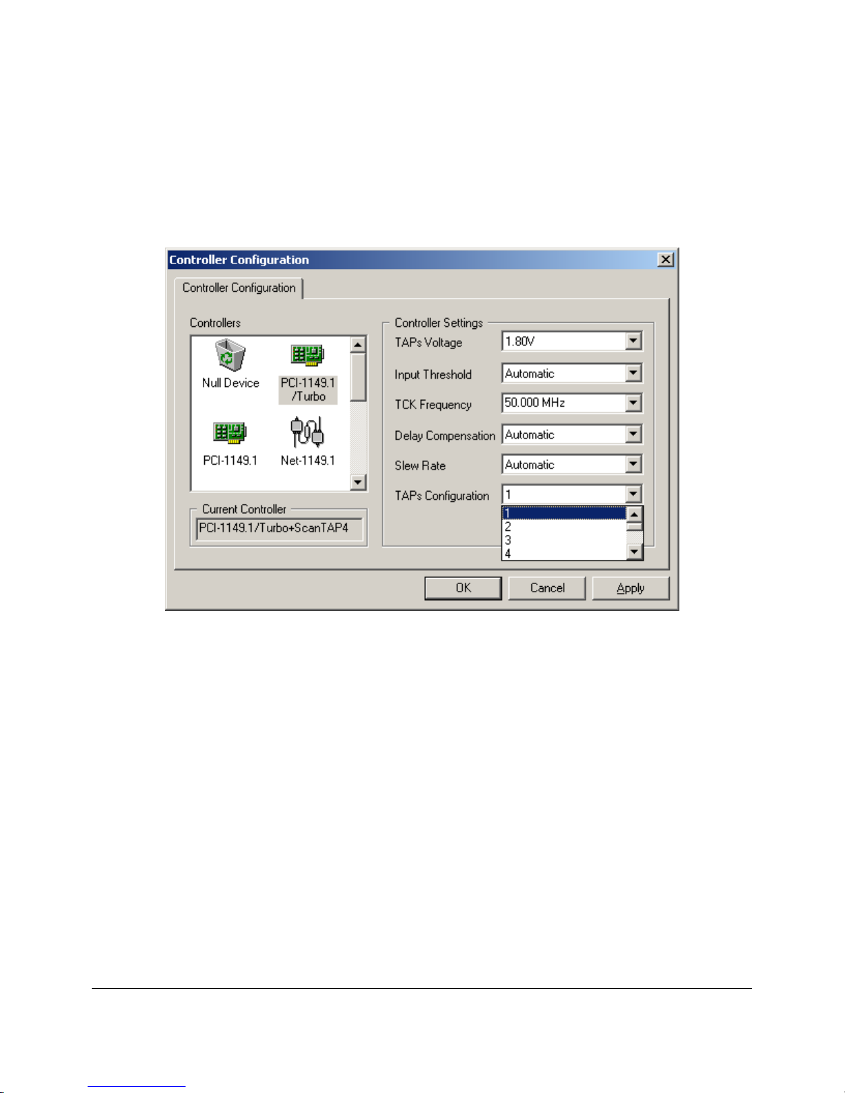
TAP Configuration - Method 1
The TAP Configuration select box in the Controller Configuration screen provides TAP
selection options as shown in Figure 4-5. This is the preferred and most straightforward method for
selecting which of the 4 ScanTAP-4 TAPs to use for connecting to the target. This feature is
available in all relevant ScanPlus Tools, including ScanPlus Runner, ScanPlus Debugger and
ScanPlus Flash Programmer.
Figure 4-5. Controller Configuration TAP Configuration Options
4-6 Using PCIe-1149.1 with ScanPlus
Page 35
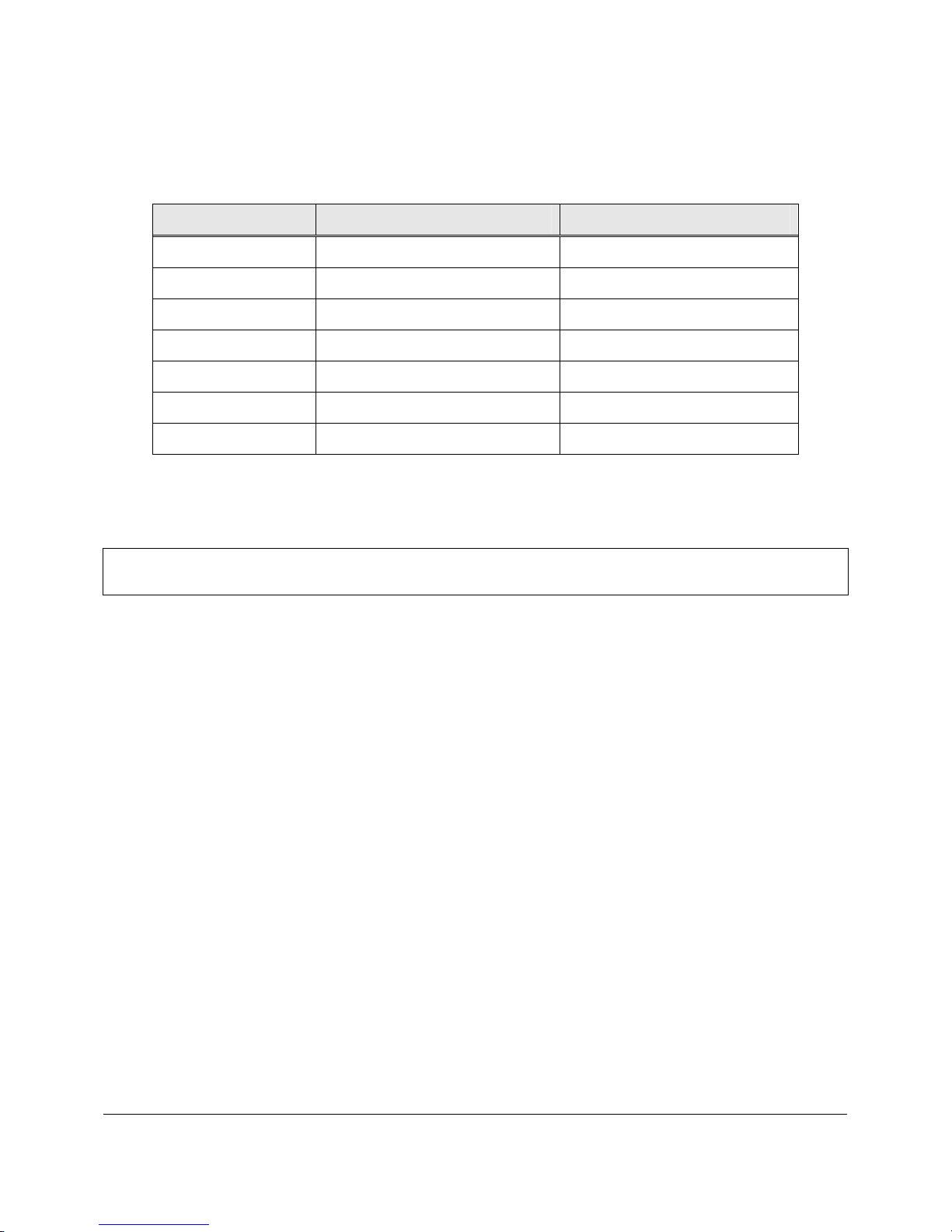
Table 4-1 summarizes the different configuration options available in the TAP Configuration drop-
down list.
Configuration Meaning TAP(s) Enabled
1 Enable TAP1 only TAP1 only
2 Enable TAP2 only TAP2 only
3 Enable TAP3 only TAP3 only
4 Enable TAP4 only TAP4 only
1+2 Serialize TAPs 1 through 2 TAPs 1 and 2 in series
1+2+3 Serialize TAPs 1 through 3 TAPs 1, 2, and 3 in series
1+2+3+4 Serialize TAPs 1 through 4 TAPs 1, 2, 3, and 4 in series
Table 4-1. ScanPlus Runner ScanTAP-4 Configuration
NOTE: Additional selection options are available for Flash Programming (.fpi) test steps as
described later in this chapter.
Using PCIe-1149.1 with ScanPlus 4-7
Page 36
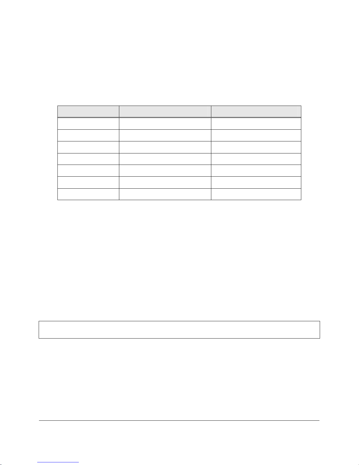
TAP Configuration - Method 2
This method is primarily provided for upwards compatibility with legacy tools and is not
recommended for new applications. It works by embedding the TAP selection text as part of the
test step file name. This method will override any TAP configuration selected in Method 1. This
feature is available in all relevant ScanPlus Tools, including ScanPlus Runner, ScanPlus Debugger
and ScanPlus Flash Programmer.
File Name ID Meaning TAP(s) Enabled
_TAP1 Enable TAP1 only TAP1 only
_TAP2 Enable TAP2 only TAP2 only
_TAP3 Enable TAP3 only TAP3 only
_TAP4 Enable TAP4 only TAP4 only
_TAP1+2 Serialize TAPs 1 through 2 TAPs 1 and 2 in series
_TAP1+2+3 Serialize TAPs 1 through 3 TAPs 1, 2, and 3 in series
_TAP1+2+3+4 Serialize TAPs 1 through 4 TAPs 1, 2, 3, and 4 in series
Table 4-2. ScanPlus Runner Naming Conventions
For example, to execute a test or programming file on a target board that contains 3 TAPs using the
file myboard_inf.cvf, change the file name to myboard_TAP1+2+3_inf.cvf. The ScanTAP-4 is
configurable on the fly, and adding a filename suffix from Table 4-2 to a test file name will configure
the system to run that test.
Note that since in most cases the file name already contains a suffix, the file name ID is inserted
between the suffix and the rest of the file name. For example, infrastructure_inf.cvf becomes
infrastructure_TAP1+2+3+4_inf.cvf.
NOTE: Additional selection options are available for Flash Programming (.fpi) test steps as
described later in this chapter.
4-8 Using PCIe-1149.1 with ScanPlus
Page 37
TAP Configuration - Method 3
This method is only available for ScanPlus Runner. It is available in the ScanPlus Runner Options
menu. Use this method only when specific test step(s) require TAP configuration settings different
from the global settings selected in Method 1.
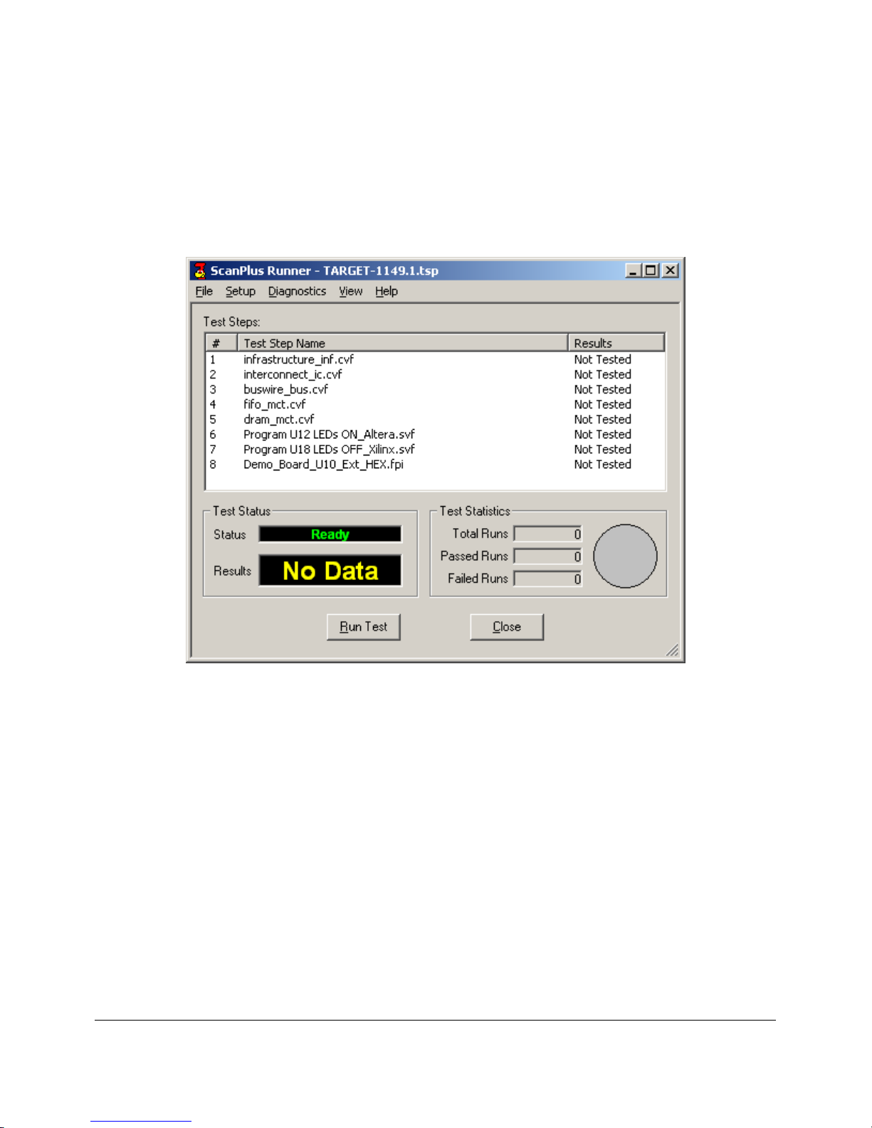
A typical ScanPlus Runner main screen with multiple test steps is shown in Figure 4-6:
Figure 4-6. Typical ScanPlus Runner Test Plan
Using PCIe-1149.1 with ScanPlus 4-9
Page 38
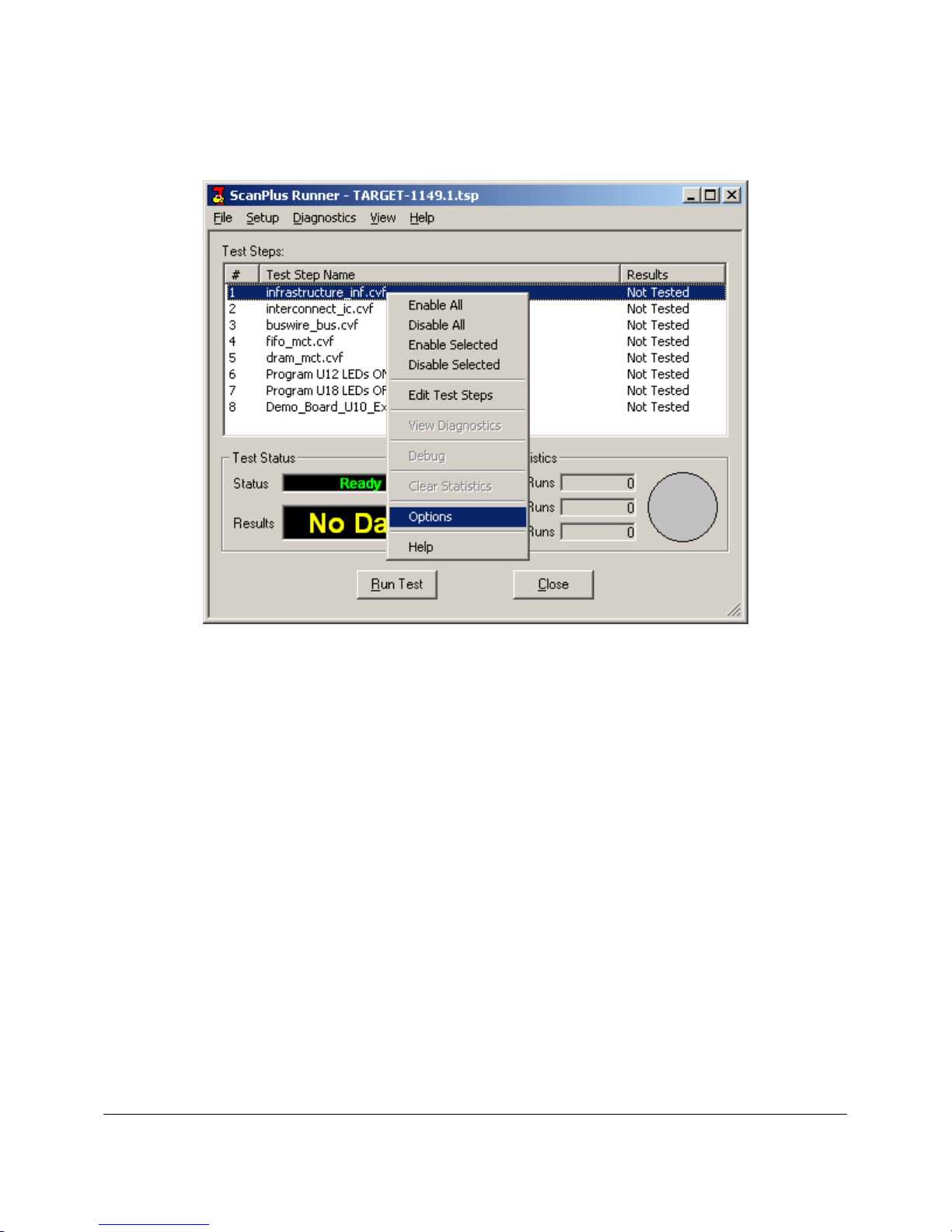
Highlight a test step by pointing to it with the mouse and then clicking once with the left mouse
button. The test step is now highlighted. Right-click on the test step name to bring up a pop-up
menu, and select Options as shown in Figure 4-7.
Figure 4-7. ScanPlus Runner Pop-up Menu
4-10 Using PCIe-1149.1 with ScanPlus
Page 39
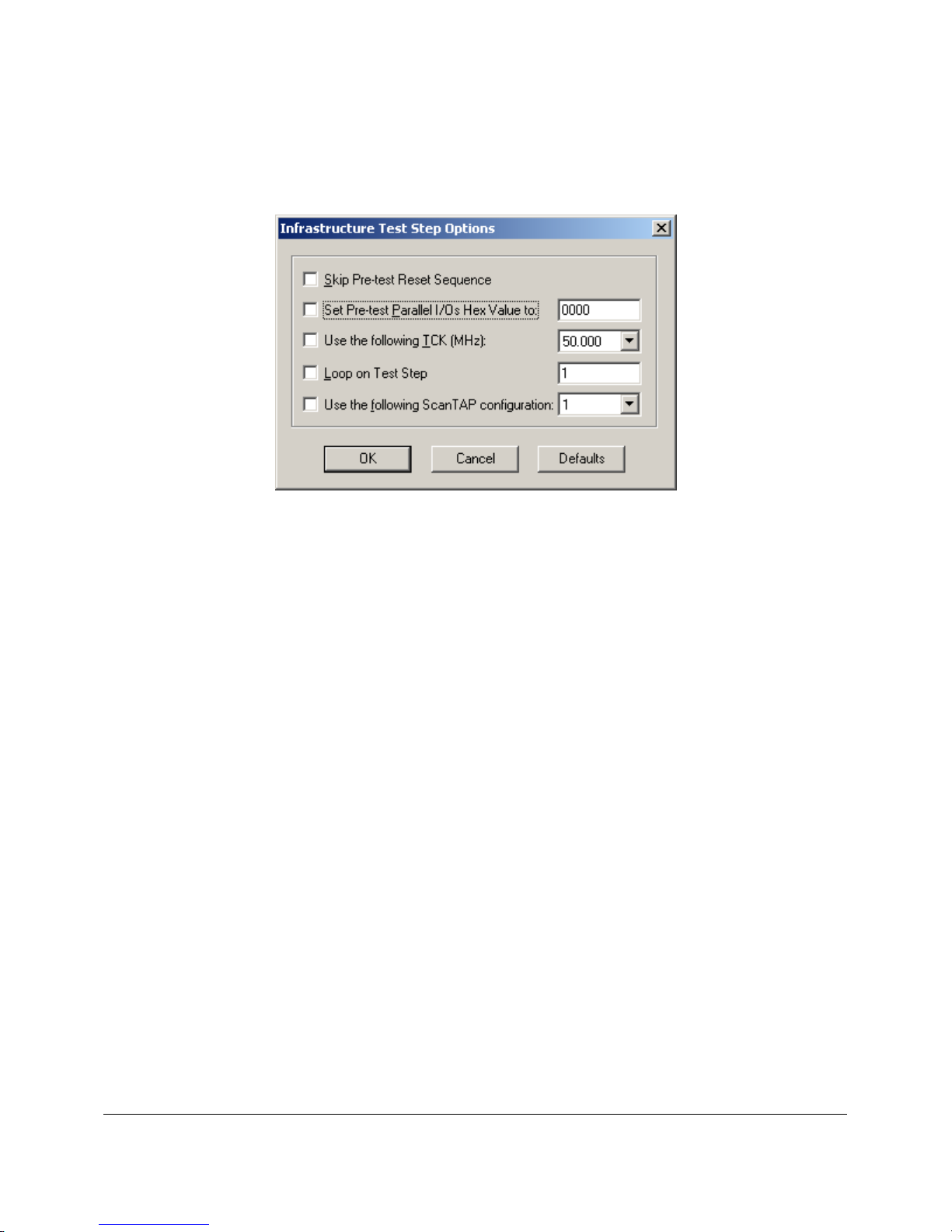
An Options dialog box similar to Figure 4-8 will appear. The appearance of the dialog box varies
with the type of test step selected. Figure 4-8 illustrates an options dialog for an infrastructure test
step. Consult the ScanPlus Runner User’s Manual for more information on the Options dialog
boxes.
Figure 4-8. Infrastructure Test Options Dialog Box
Using PCIe-1149.1 with ScanPlus 4-11
Page 40
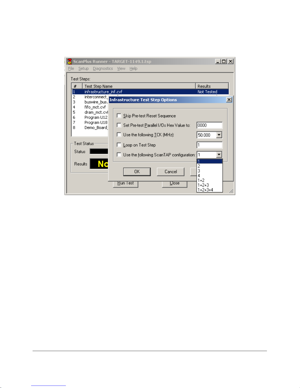
Click the Use the following ScanTAP configuration check box and select the desired
programming topology configuration from the drop-down list. Figure 4-9 shows the selections
available from the configuration drop-down list.
Figure 4-9. Available ScanTAP-4 Configuration
4-12 Using PCIe-1149.1 with ScanPlus
Page 41
Gang Programming with ScanPlus Runner
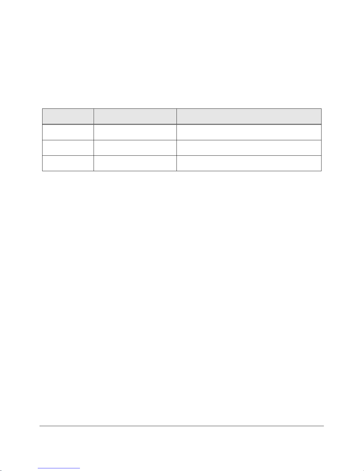
Special TAP configuration features are provi ded fo r paral l e l (Ga ng ) pr o gr amming of Flash memories using .fpi files.
ScanPlus Runner also supports gang programming, determining the configuration of the Flash programming
topology from the .fpi file name. This is in addition to the TAP configuration options listed .
Table 4-3 lists suffixes to add to the file name for various cases:
File Name ID Meaning TAP(s) Enabled
_TAP1-2 Enable TAPs 1 through 2 Gang Programming of TAP1 and TAP2
_TAP1-3 Enable TAPs 1 through 3 Gang Programming of TAP1, TAP2 and TAP 3
_TAP1-4 Enable TAPs 1 through 4 Gang Programming of TAPs 1, 2, 3 and 4
Table 4-3. ScanPlus Runner Naming Conventions for Gang Programming
For example, to gang program all four target boards using the file program U7.fpi, change the file
name to program U7_TAP1-4.fpi. The ScanTAP-4 is configurable on the fly, and adding a
filename suffix from Table 4-3 to a test file name will configure the system to run that test.
Using PCIe-1149.1 with ScanPlus 4-13
Page 42
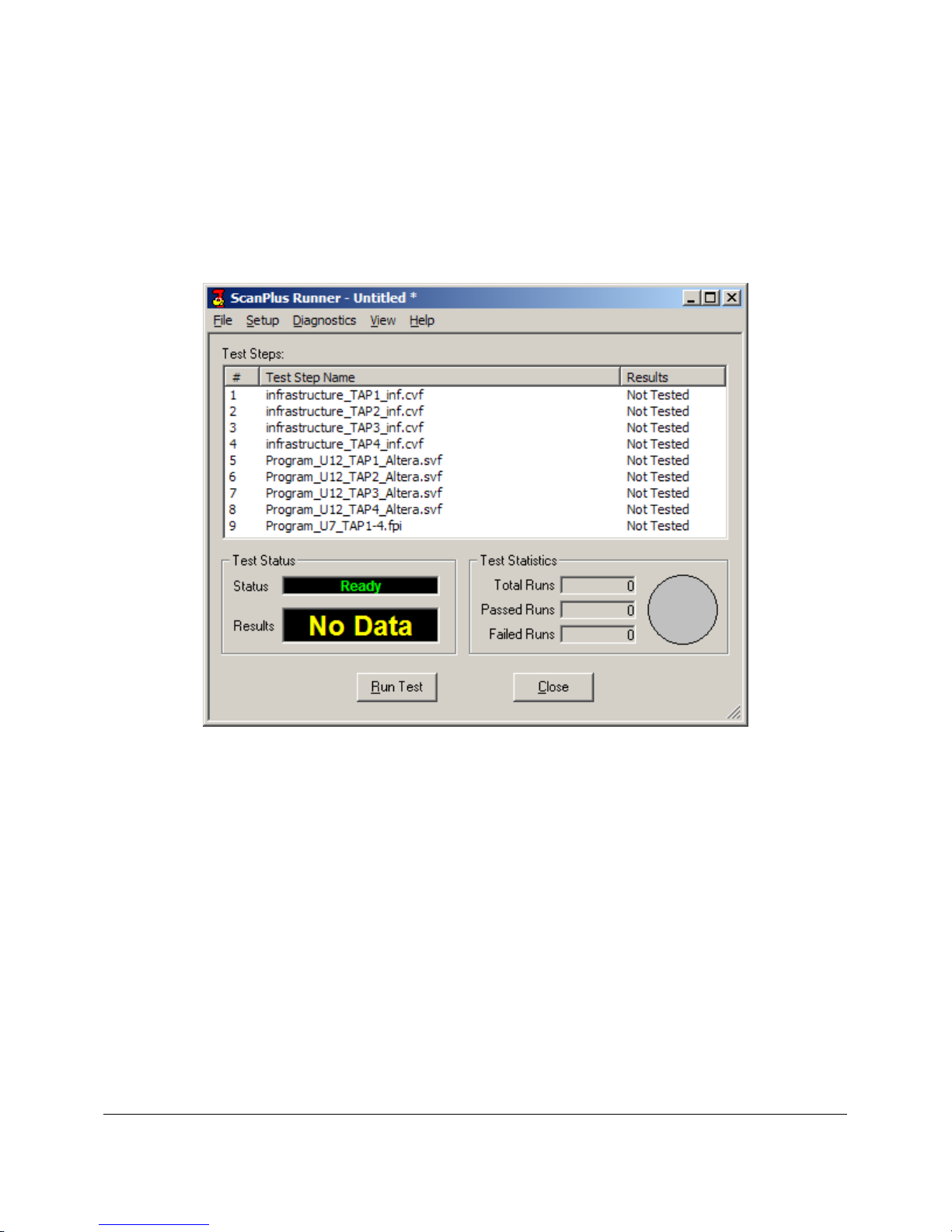
In the test plan shown in Figure 4-10 below, the system first tests target TAPs 1 through 4 for
infrastructure, then it programs the Altera CPLD on target TAPs 1 through 4, then it programs the
Flash memory in parallel on all four targets.
Note that for files that already contain a suffix, the file name ID is inserted between the suffix and
the rest of the file name. For example, infrastructure_inf.cvf becomes infrastructure_TAP1-
4_inf.cvf.
Figure 4-10. ScanPlus Runner Test Plan for Gang Programming
4-14 Using PCIe-1149.1 with ScanPlus
Page 43
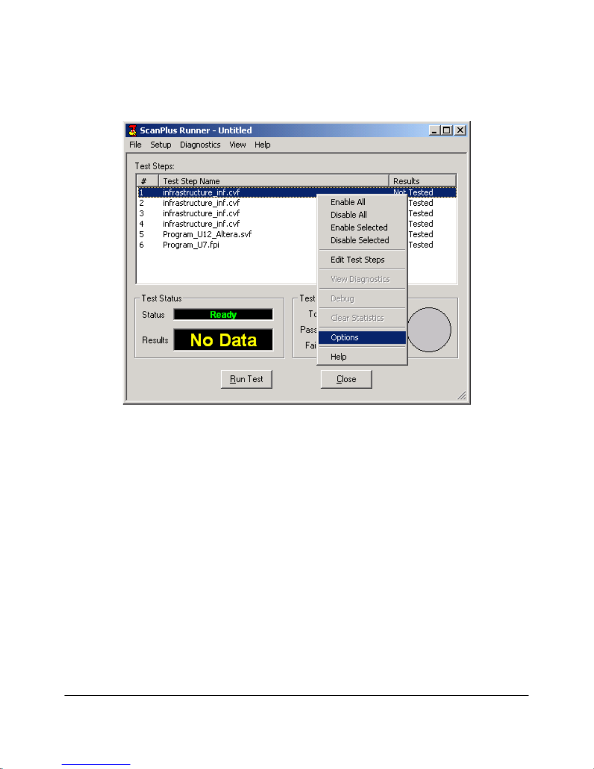
The Options dialog provides an alternate way to specify gang programming from ScanPlus Runner.
Right-click on the test step name to bring up a pop-up menu, and select Options as shown in Figure
4-11.
Figure 4-11. ScanPlus Runner Pop-up Menu
Using PCIe-1149.1 with ScanPlus 4-15
Page 44
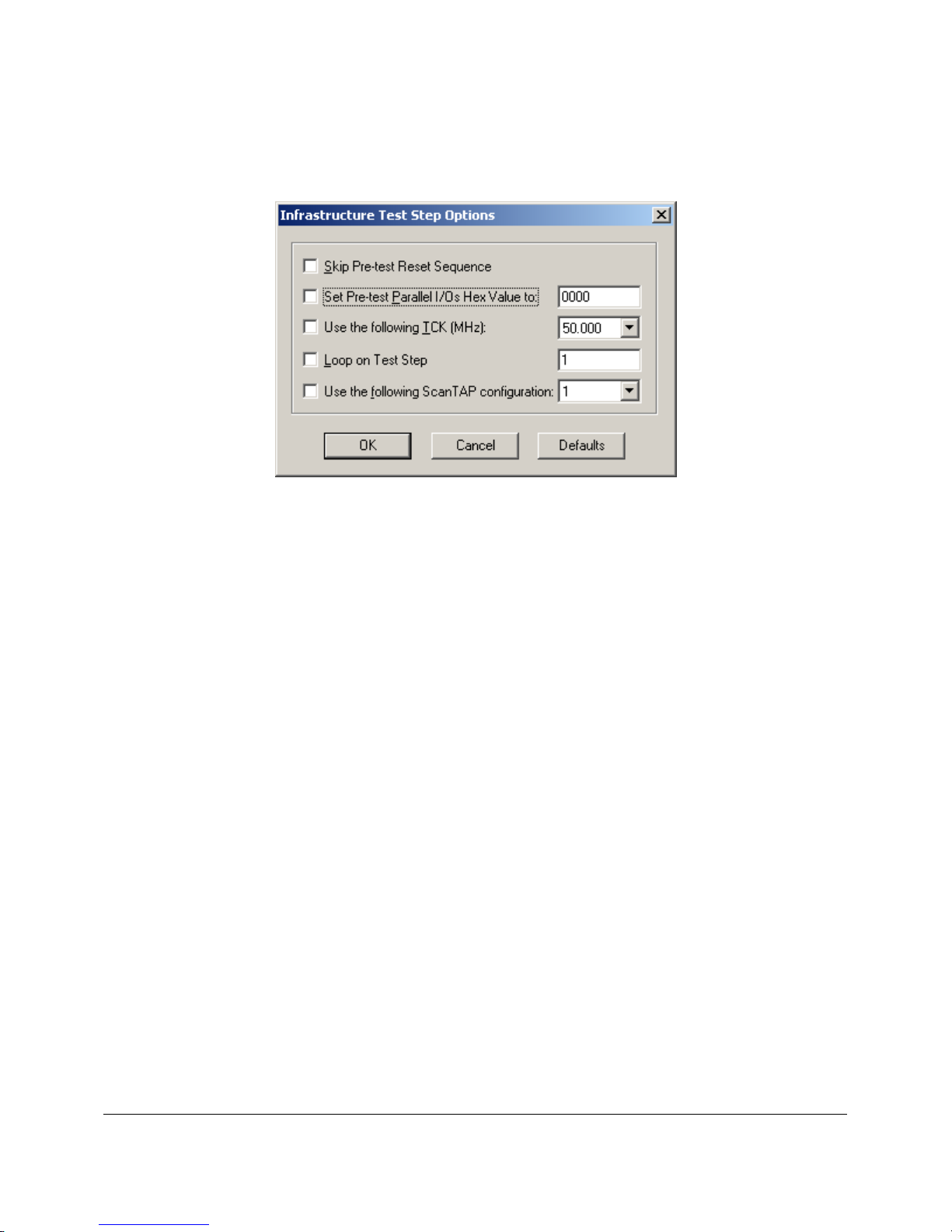
An Options dialog box similar to Figure 4-12 will appear. The appearance of the dialog box varies
with the type of test step selected. Figure 4-12 illustrates an options dialog for an infrastructure test
step. Consult the ScanPlus Runner User’s Manual for more information on the Options dialog
boxes.
Figure 4-12. Infrastructure Test Options Dialog Box
4-16 Using PCIe-1149.1 with ScanPlus
Page 45
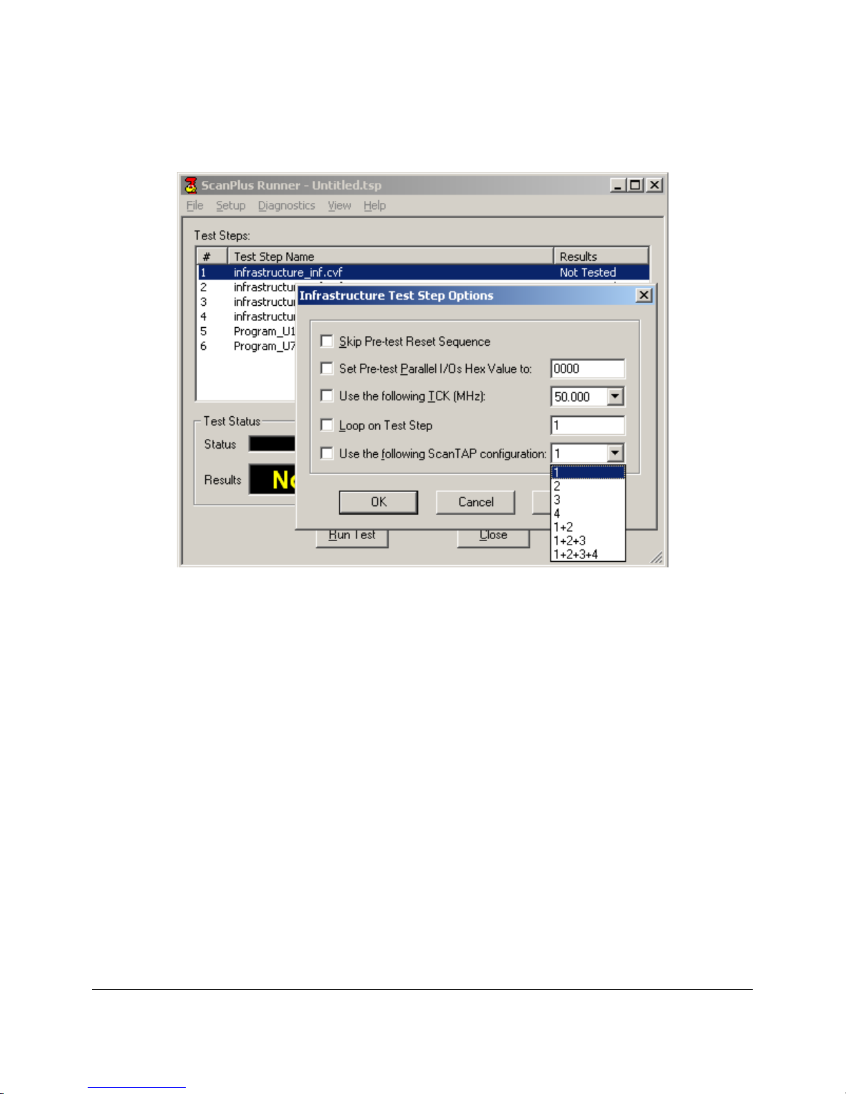
Click the Use the following ScanTAP configuration check box and select the desired
programming topology configuration from the drop-down list. Figure 4-13 shows the selections
available from the configuration drop-down list.
Figure 4-13. Available ScanTAP-4 TAP Configuration
Using PCIe-1149.1 with ScanPlus 4-17
Page 46
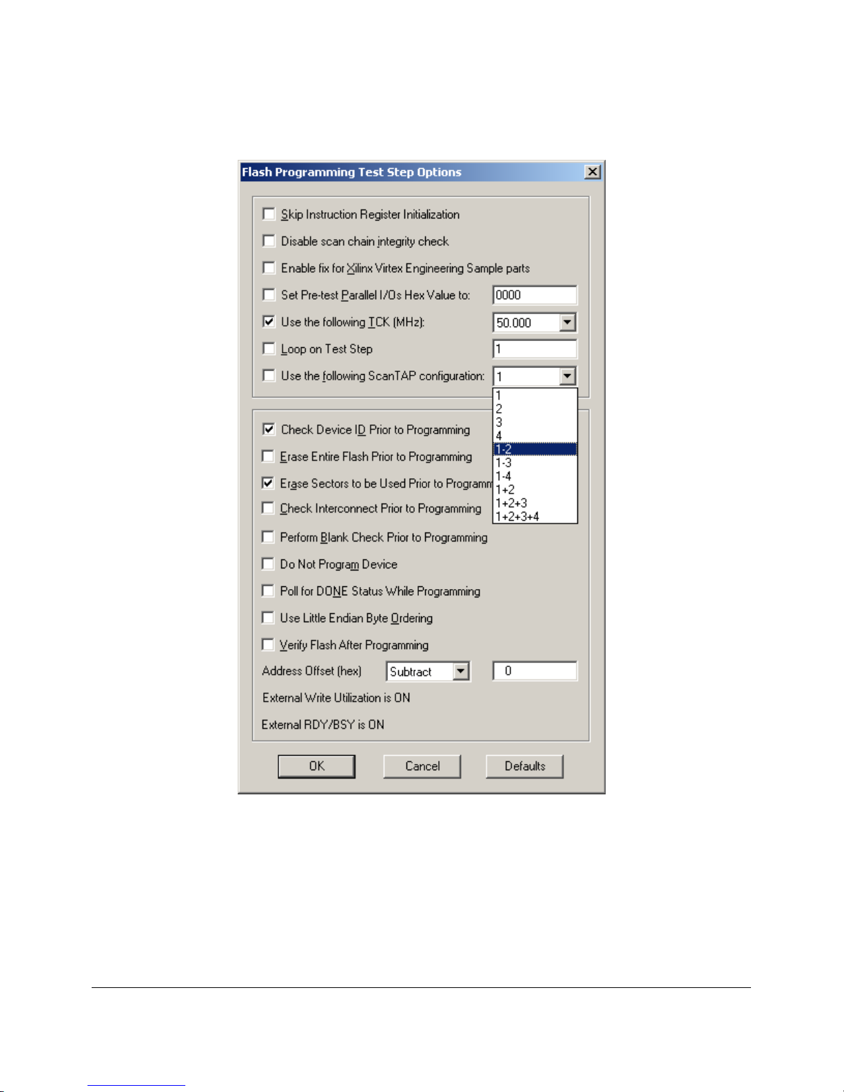
Note that the same drop-down options list contains additional configuration options for the .fpi
(programming) test steps. These additional configuration options are only available for Gang Flash
programming of .fpi files and is not shown for regular test steps (.cvf files). See Figure 4-14.
Figure 4-14. Available ScanTAP-4 TAP Configuration for .fpi files
4-18 Using PCIe-1149.1 with ScanPlus
Page 47
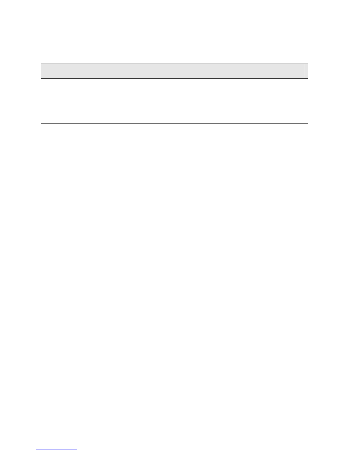
Table 4-4 summarizes the additional, .fpi file-specific, configuration options available in the dropdown list.
Configuration Meaning TAP(s) Enabled
1-2 Enable TAPs 1 through TAP2 in parallel (Gang) TAPs 1 and 2 are active
1-3 Enable TAPs 1 through TAP3 in parallel (Gang) TAPs 1, 2 and 3 active
1-4 Enable TAPs 1 through TAP4 in parallel (Gang) All 4 TAPs are active
Table 4-4. ScanPlus Runner ScanTAP-4 Configuration
Using PCIe-1149.1 with ScanPlus 4-19
Page 48
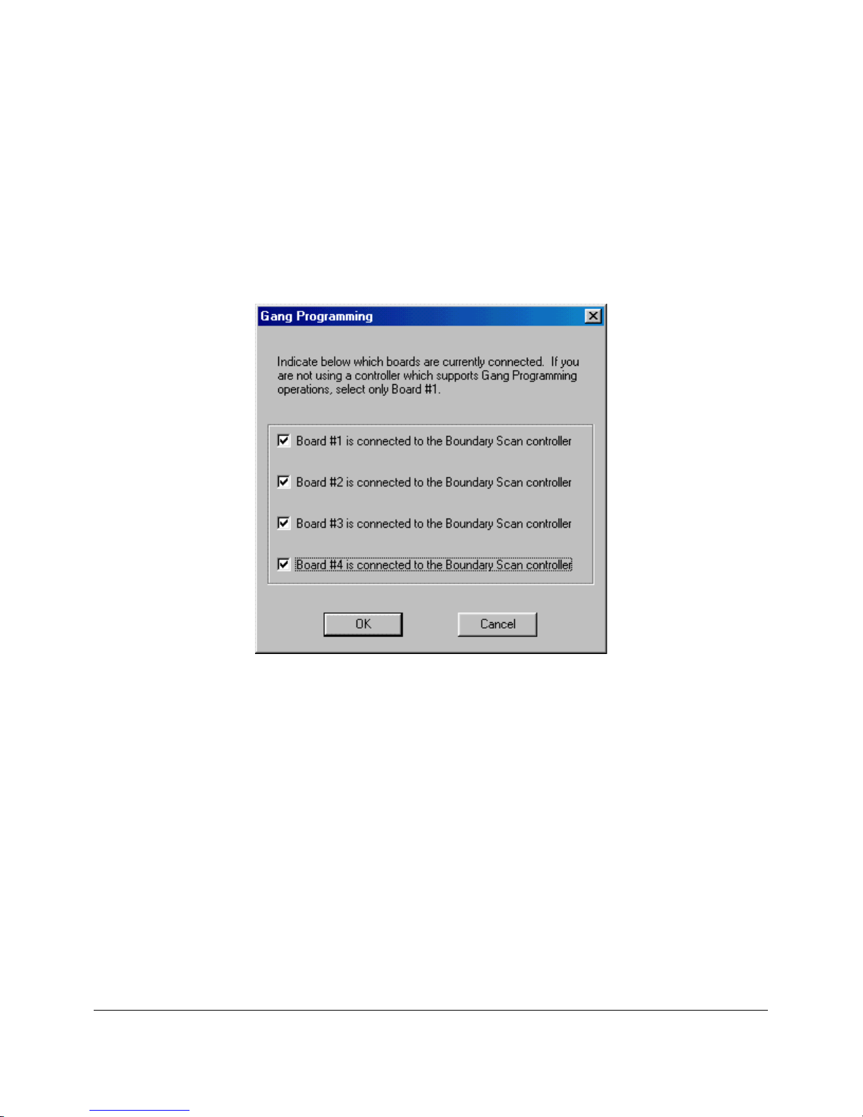
Gang Programming with ScanPlus Flash Programmer
Version 1.73 or newer of the ScanPlus Flash Programmer software supports gang programming of
multiple target boards using ScanTAP-4. Gang programming with the ScanTAP-4 requires an .fpi
file that the ScanPlus Flash Generator generates. Gang programming applies the same .fpi file to
identical targets concurrently via separate TAP connections.
Invoke ScanPlus Flash Programmer, select the Setup menu item, and the Gang Programming entry. Then check
off the TAPs on which you are programming the Flash Devices.
Figure 4-15 below shows the setup for programming four targets in parallel.
Figure 4-15. ScanPlus Flash Programmer Gang Programming Window
4-20 Using PCIe-1149.1 with ScanPlus
Page 49
Chapter 5
Third Party Application Interface
ScanPlus Runner provides a general purpose, third-party application interface that includes
specifying the correct controller card and settings. This section clarifies the requirements related to
the PCIe-1149.1 card and to the ScanTAP-4. Refer to the ScanPlus Runner manual for further
information.
Using PCIe-1149.1 with ScanPlus Runner Command-line
You can invoke ScanPlus Runner with special command line parameters to execute a Test Step file,
provide test results and diagnostic messages in a log file (if you have the ScanPlus Runner ADO),
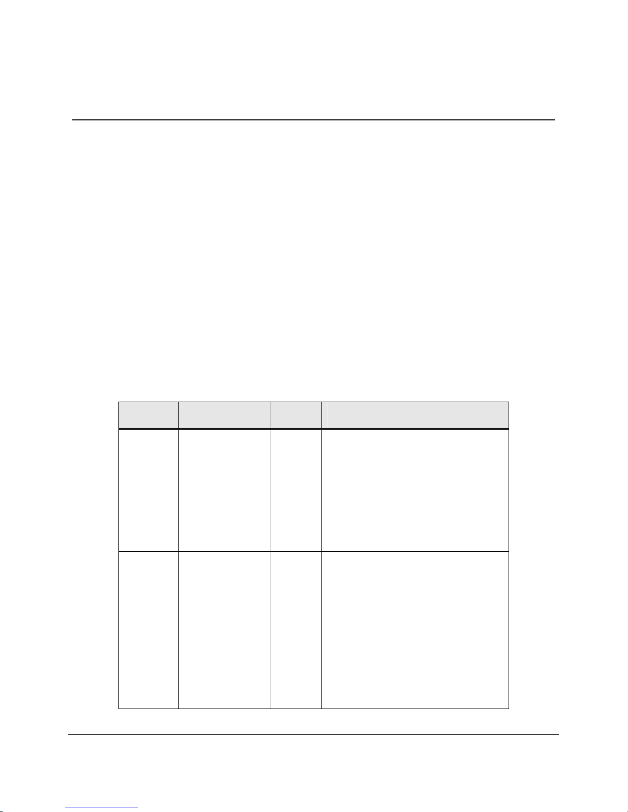
and then terminate. The following table shows the controller identifiers and associated parameters.
Consult the ScanPlus Runner User’s Manual for more detail.
The PCIe-1149.1 controller without ScanTAP4 uses three parameters and it uses up to fourteen
parameters with ScanTAP4. The parameters are described in the table below.
Controller keyword: PCIe-1149.1, PCIe-1149.1+ScanTAP4
Position Parameter Value Setting
1 TAPs Voltage 1
2
…
41
42
43
2 Clock Frequency 51
…
76
77
1.25 V
1.30 V
… (0.05 volts per step)
3.25 V
3.30 V
Use advanced voltage settings in
position 7 through 10
80 MHz
… (1 MHz increment)
25 MHz
24.5 MHz
Third Party Application Interface 5-1
…
101
… (0.5 MHz increment)
12.5 MHz
Page 50
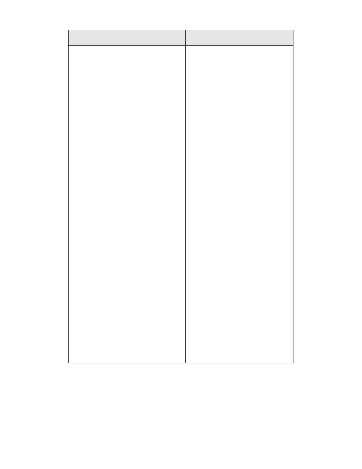
Position Parameter Value Setting
102
…
126
127
…
136
137
…
161
162
…
186
12.25 MHz
… (0.25 MHz increment)
6.25 MHz
6.125 MHz
… (0.125 MHz increment)
5 MHz
4.9 MHz
… (0.1 MHz increment)
2.5 MHz
2.45 MHz
… (0.05 MHz increment)
1.25 MHz
187
…
211
212
…
226
227
…
233
1.225 MHz
… (0.025 MHz increment)
.625 MHz
.609MHz
… (0.0156 MHz increment)
.391MHz
.350 MHz
… (0.05 MHz increment)
.050 MHz
Table 5-1. PCIe-1149.1 Controller Parameters
5-2 Third Party Application Interface
Page 51

Position Parameter Value Setting
3 Delay
Compensation
1
2
3
4
5
6
7
8
…
31
32
Automatic
No Delay
0.5 Clock Delay
1.0 Clock Delay
1.5 Clock Delay
2.0 Clock Delay
2.5 Clock Delay
(the following are for PCIe-1149.1
without ScanTAP only)
3.0 Clock Delay
… (0.5 clock increment)
14.5 Clock Delay
15.0 Clock Delay
4 Input Threshold 1 2 Automatic
Use advanced input threshold
settings in position 11 through 14
5 Slew Rate 1
2
3
6 TAPs
Configuration
1
2
3
4
5
5
7
Automatic
Slow slew rate
Normal slew rate
Use TAP1
Use TAP2
Use TAP3
Use TAP4
Use TAPs 1 and 2 in series
Use TAPs 1, 2, and 3 in series
Use TAPs 1, 2, 3, and 4 in series
Third Party Application Interface 5-3
Page 52

Position Parameter Value Setting
7 TAP1 Voltage 1
2
3
…
40
41
42
8 TAP2 Voltage 1
2
3
…
40
41
42
9 TAP3 Voltage 1
2
3
…
40
41
42
1.25 V
1.30 V
1.35 V
… (0.05 V per step)
3.20 V
3.25 V
3.30 V
1.25 V
1.30 V
1.35 V
… (0.05 V per step)
3.20 V
3.25 V
3.30 V
1.25 V
1.30 V
1.35 V
… (0.05 V per step)
3.20 V
3.25 V
3.30 V
10 TAP4 Voltage 1
2
3
…
40
41
42
11 TAP1
1 Automatic
1.25 V
1.30 V
1.35 V
… (0.05 V per step)
3.20 V
3.25 V
3.30 V
Input Threshold
12 TAP2
1 Automatic
Input Threshold
13 TAP3
1 Automatic
Input Threshold
14 TAP4
1 Automatic
Input Threshold
Table 5-1. PCIe-1149.1 Controller Parameters (continued)
5-4 Third Party Application Interface
Page 53

Example:
To select a PCIe-1149.1 controller card with a TAP1 voltage of 3.30 V, TCK frequency of 1 MHz,
and automatic delay compensation, use this “controller specification” string:
-controller “PCIe-1149.1,42,196,1,,,,”
To select a PCIe-1149.1+ScanTAP4 controller card with all TAP voltages of 3.30 V, TCK frequency
of 1 MHz, automatic delay compensation, automatic input threshold, slow slew rate and TAP1, use
this “controller specification” string:
-controller “PCIe-1149.1+ScanTAP4,42,196,1,1,1,1,42,42,42,42,1,1,1,1”
Third Party Application Interface 5-5
Page 54

Page 55
Appendix A
Recommended Target Connector s
10-pin TAP Connector
The Boundary-Scan TAP is a well defined IEEE-1149.1-compatible electrical interface between
boundary-scan test equipment and the boundary-scan compatible devices in the user’s target board.
Boundary-scan based test equipment, such as the Corelis ScanPlus family of products, utilize a single
TAP to interface to the UUT. This section explains how to implement a TAP connector that is
compatible with most standard test equipment.
The TAP contains 5 signals: TCK, TMS, TDO, TDI and optionally TRST*. It also contains ground
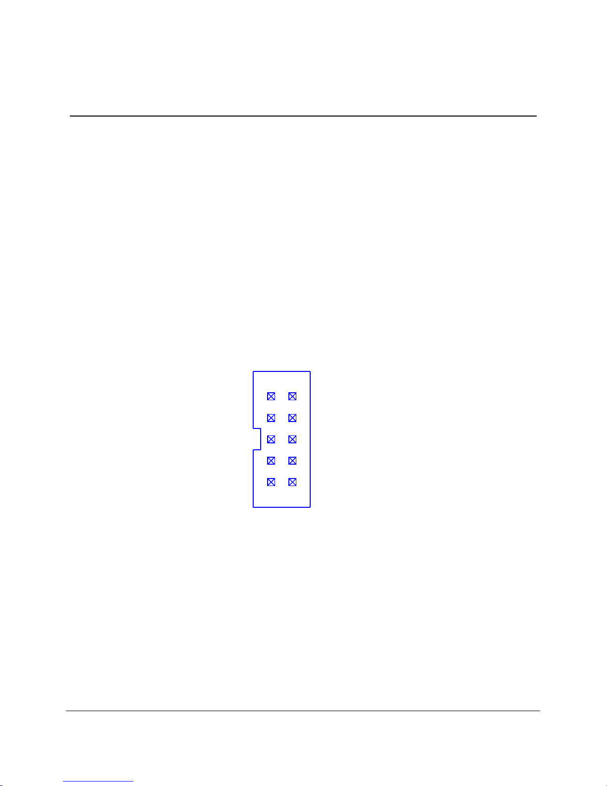
signal(s). Corelis recommends the standard TAP connector shown in Figure A-1, which is widely
regarded as the industry standard. Note that each signal is terminated with a resistor (discussed
below) in order to improve noise immunity.
The connector on the user’s target should have a standard flat cable compatible pinout to match the
TAP connector described in Table A-1. Figure A-1 shows the top view of the basic target 10-pin
connector header (0.100 × 0.100 in. spacing):
GND
TRST* 1
TDI 3
TDO 5
TMS 7
TCK 9
2
4 GND
6 GND
8 GND
10 GND
Figure A-1. Standard TAP conn
ector (top view)
Recommended Target Connectors A-1
Page 56
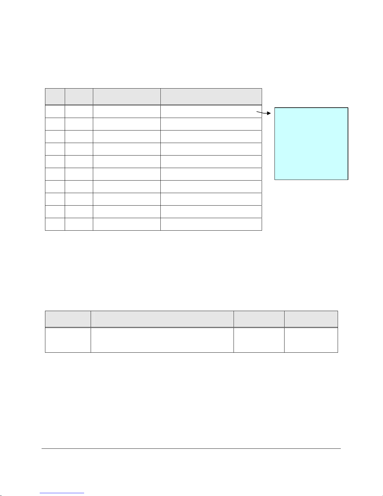
Table A-1 describes the 10 pin TAP connector signals and Corelis recommended values of
terminating resistors:
Pin Signal Direction Termination
1 TRST* Input to the UUT 1K pull-up (or 1.5K pull-down)
2 GND
3 TDI Input to the UUT 1K pull-up
4 GND
5 TDO Output of the UUT 33 ohm series
6 GND
Note: Some target
boards may require a
pull-down resistor on
the TRST* signal to
assure normal device
operations when not
in boundary-scan test
mode.
7 TMS Input to the UUT 1K pull-up
8 GND
9 TCK Input to the UUT 1K pull-up
10 GND
Table A-1. Signal Description and Termination
Table A-2 summarizes the specifications for the 10-pin TAP connector. Equivalent connectors are
available from other manufacturers.
Reference Description Manufacturer Part Number
10-Pin
Target TAP
Straight header, 10-pin, 4 wall, with center
notch
Table A-2. Standard 10-Pin TAP Connector
3M 3473-6610
A-2 Recommended Target Connectors
Page 57
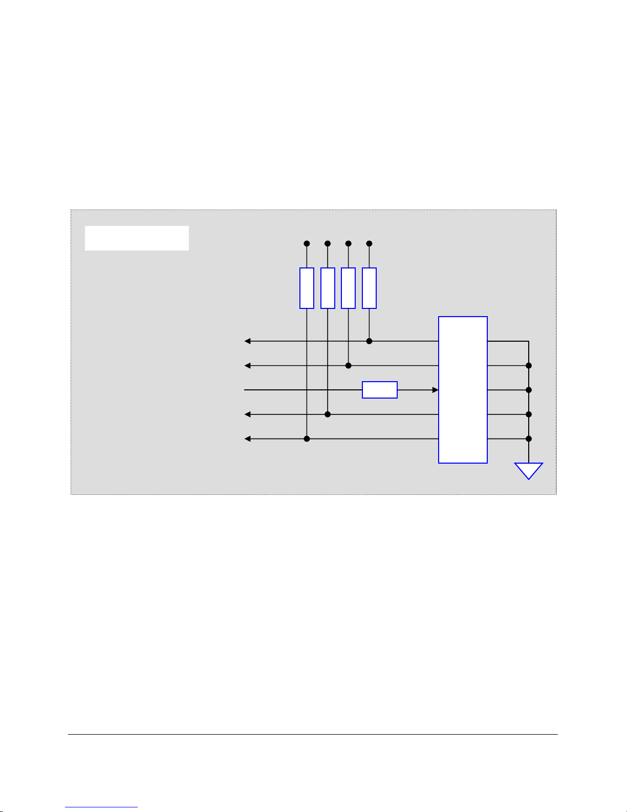
Figure A-2 shows a typical schematic of the target TAP
connector with the recommended
termination resistors. The 1K pull-up resistors should connect to the target Vcc supply
corresponding to the interface voltage (programmable on the PCIe-1149.1 from 1.25 to 3.3 V).
Recommended resistor values are +/- 5%.
Target Board
To all Boundary-Scan Devices
To TDI of 1st Device in the chain
From TDO of last Device in chain
To all Boundary-Scan Devices
To all Boundary-Scan Devices
Vcc Vcc Vcc Vcc
1K
1K 1K 1K
33
TRST*
TDI
TDO
TMS
TCK
2
1
4
3
6
5
8
7
9
10
TAP
Connector
Recommended Target Connectors A-3
Figure A-2. TAP Connector Schematic
Page 58
Flash Programming TAP Connector
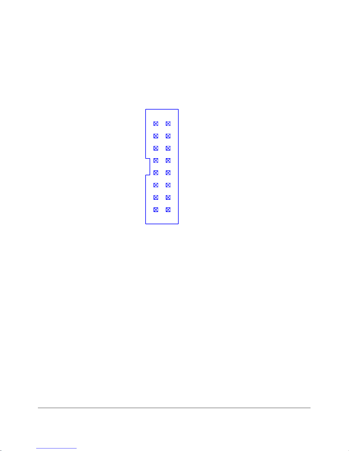
To build in support for in-circuit programming of flash or microprocessor devices, Corelis
recommends including supplemental control signals in the TAP interface. The ScanPlus Flash
Programmer can use a 16-pin TAP, similar to Figure A-3, to improve programming time. This
interface adds Write_Strobe*, Ready/Busy*, and ground signals to the standard 5-signal interface.
Terminating resistors (see Table) can improve signal quality.
TRST* 1
TDI 3
TDO 5
TMS 7
Write_Strobe* 11
TCK 9
Reserved 13
Ready/Busy
* 15 16 Do Not Connect
2 GND
4
GND
6 GND
8 GND
10
GND
12 GND
14
Do Not Connect
Figure A-3. Boundary-scan Flash Programming 16 Pin TAP Connector (top view)
Corelis’ Flash Programming software supports the external signals Write_Strobe* and Ready/Busy*,
in addition to the standard but slower scanned out/in signals approach.
The Write_Strobe* signal is active low and should be pulled up with a 1K resistor on the target
board. It needs to be logically ORed with the flash Write-Enable (WE*) signal so that either the
flash Write-Enable (WE*) signal or the external Write_Strobe* going low will assert the flash WE*
input.
The active low Ready/Busy* signal is typically an open-collector/open-drain signal that ties directly
to the same signal(s) on the Flash device(s). This enables multiple devices to drive it toward the
PCIe-1149.1.
A-4 Recommended Target Connectors
Page 59
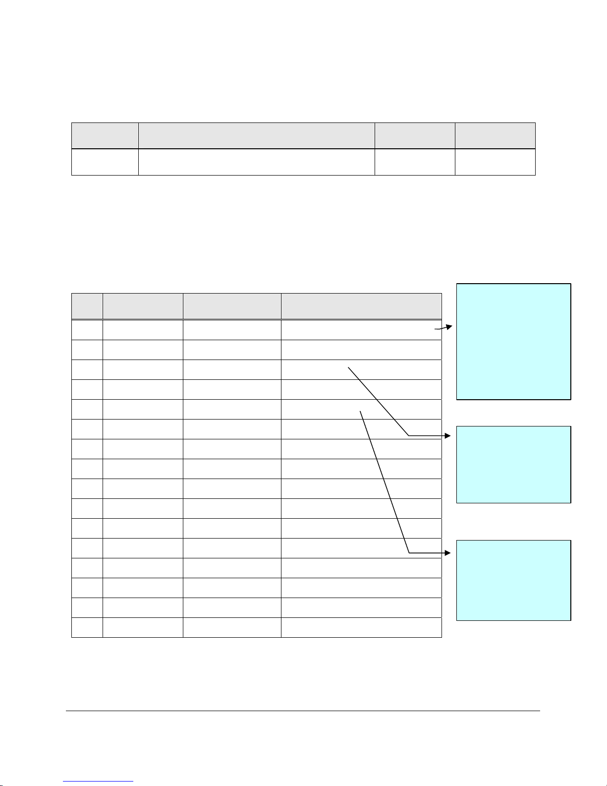
Table A-3 summarizes the specifications for a 16-pin TAP connector without latch ejector.
Equivalent connectors are available from other manufacturers.
Reference Description Manufacturer Part Number
Flash TAP Straight header, 16-pin, 4 wall, with center notch 3M 2516-6002UG
Table A-3. Flash Programming TAP 16 Pin Connector
Table A-4 describes the signals and Corelis recommended values of terminating resistors:
Note: Some target
Pin Signal Direction Termination
boards may require a
pull-down resistor on
1 TRST* Input to the UUT 1K pull-up (or 1.5K pull-down)
2 GND
3 TDI Input to the UUT 1K pull-up
4 GND
the TRST* signal to
assure normal device
operations when not
in boundary-scan test
mode
5 TDO Output from UUT 33 ohm series
6 GND
7 TMS Input to the UUT 1K pull-up
8 GND
9 TCK Input to the UUT 1K pull-up
10 GND
11 Write_Strobe* Input to the UUT 1K pull-up
12 GND
13 Reserved
14 Reserved
15 Ready/Busy* Output from UUT 1K pull-up
16 Reserved
Table A-4. Signal Description and Termination
Note: The target
TDI signal is driven
by the TDO signal of
the boundary-scan
controller
Note: The target
TDO signal drives
the boundary scan
controller’s TDI
signal
Recommended Target Connectors A-5
Page 60
K
r
Figure A-4 shows a typical schematic of the target TAP connector with termination resistors. The
1K pull-up resistors should connect to the target Vcc supply corresponding to the interface voltage
(programmable on the PCIe-1149.1 from 1.25 to 3.3 V). Recommended resistor values are +/- 5%.
Target Board
To all Boundary Scan Devices
To TDI of 1st Device in the chain
From TDO o
To all Boundary Scan Devices
To all Boundary Scan Devices
To flash device(s) WE* control
From flash Read/Busy* pin(s)
f last Device in chain
Vcc Vcc
1K 1K
Vcc
1K
Vcc Vcc Vcc
1K 1K 1K
TRST*
TDI
TDO
33
TMS
TC
Connecto
1
3
5
7
9
11
13
15
2
4
6
8
10
12
14
16
TAP
Figure A-4. Flash Programming TAP Connector Schematics
A-6 Recommended Target Connectors
Page 61
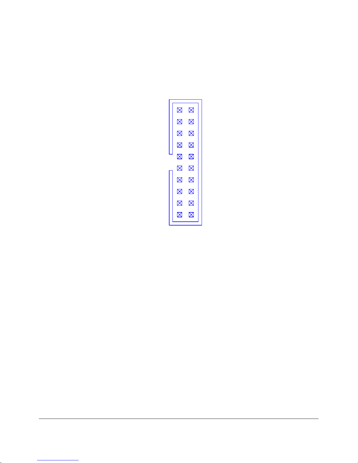
20-pin TAP Connector
To build in support for in-circuit programming of flash or microprocessor devices, Corelis
recommends including supplemental control signals in the TAP interface. The ScanPlus Flash
Programmer can use a 16-pin TAP, similar to Figure A-5, to improve programming time. This
interface adds Write_Strobe*, Ready/Busy*, and ground signals to the standard 5-signal interface.
Terminating resistors (see Table) can improve signal quality.
TRST* 1
TDI 3
TDO 5
TMS 7
TCK 9
Write_Strobe* / GPIO1 / SPI_CS2* 11
SPI_SCK / GPIO2 13
Ready_Busy* / SPI_SDO / GPIO3 15
UUT Power Test Point 17
UUT Power Test Point 19
2 GND
4 GND
6 GND
8 GND
10 GND
12 GND
14 GND
16 SPI_SDI
18 I2C_SCL
20 SPI_CS1* / I2C_SDA
Figure A-5. Boundary-scan Flash Programming 20-Pin TAP Connector (top view)
Corelis’ Flash Programming software supports the external signals Write_Strobe* and Ready/Busy*,
in addition to the standard but slower scanned out/in signals approach.
The Write_Strobe* signal is active low and should be pulled up with a 1K resistor on the target
board. It needs to be logically ORed with the flash Write-Enable (WE*) signal so that either the
flash Write-Enable (WE*) signal or the external Write_Strobe* going low will assert the flash WE*
input.
The active low Ready/Busy* signal is typically an open-collector/open-drain signal that ties directly
to the same signal(s) on the Flash device(s). This enables multiple devices to drive it toward the
PCIe-1149.1.
Recommended Target Connectors A-7
Page 62
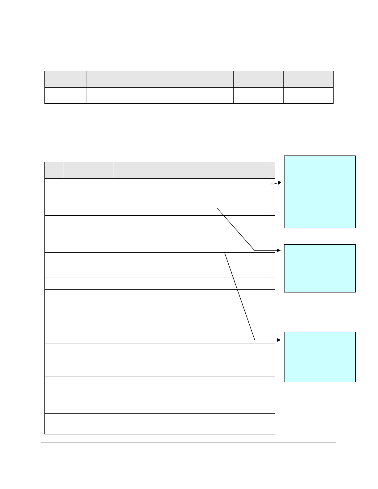
Table A-3 summarizes the specifications for a 16-pin TAP connector without latch ejector.
Equivalent connectors are available from other manufacturers.
Reference Description Manufacturer Part Number
Flash TAP Straight header, 16-pin, 4 wall, with center notch 3M 2516-6002UG
Table A-5. Flash Programming TAP 16 Pin Connector
Table A-4 describes the signals and Corelis recommended values of terminating resistors:
Note: Some target
Pin Signal Direction Termination
boards may require a
pull-down resistor on
1 TRST* Input to the UUT 1K pull-up (or 1.5K pull-down)
2 GND
3 TDI Input to the UUT 1K pull-up
4 GND
the TRST* signal to
assure normal device
operations when not
in boundary-scan test
mode
5 TDO Output from UUT 33 ohm series
6 GND
7 TMS Input to the UUT 1K pull-up
8 GND
9 TCK Input to the UUT 1K pull-up
10 GND
Write_Strobe*
11
/GPIO1 /
Input to the UUT 1K pull-up
SPI_CS2*
12 GND
SPI_SCK
13
/GPIO2
Input to the UUT 1K pull-up
14 GND
Ready_Busy*
15
/ SPI_SDO
(MISO) /
Output from the
UUT
1K pull-up
GPIO3
Note: The target
TDI signal is driven
by the TDO signal of
the boundary-scan
controller
Note: The target
TDO signal drives
the boundary scan
controller’s TDI
signal
SPI_SDI
16
(MOSI)
Input to the UUT 1K pull-up
A-8 Recommended Target Connectors
Page 63

17 VCC1
UUT Power Test
Point
18 I2C_SCL Input to the UUT 1K pull-up
19 VCC2
SPI_CS1* /
20
I2C_SDA
UUT Power Test
Point
Input to the UUT 1K pull-up
Table A-6. Signal Description and Termination
Recommended Target Connectors A-9
Page 64
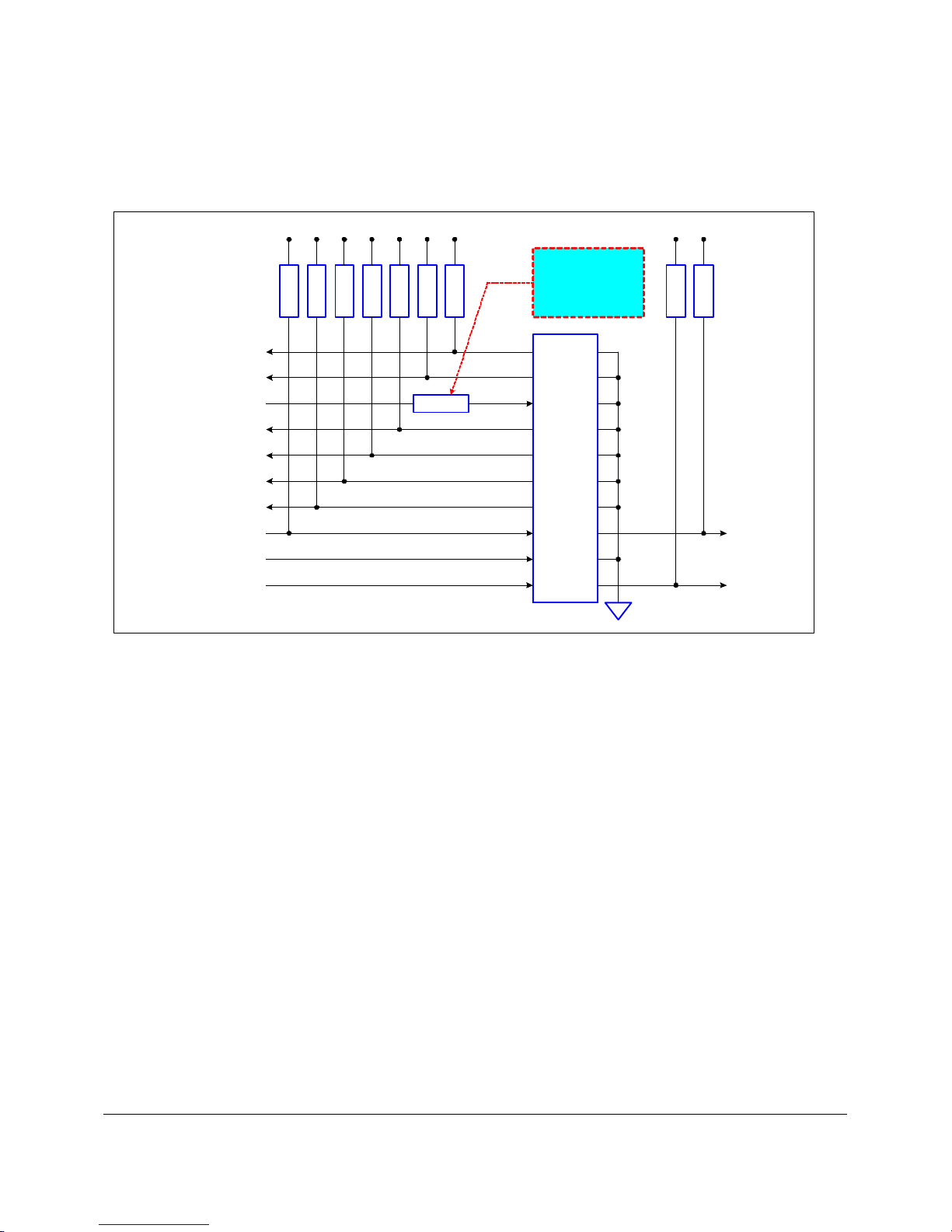
Figure A-6 shows a typical schematic of the target TAP connector with termination resistors. The
1K pull-up resistors should connect to the target Vcc supply corresponding to the interface voltage
(programmable on the PCIe-1149.1 from 1.25 to 3.3 V). Recommended resistor values are +/- 5%.
VccVccVccVccVccVccVccVccVcc
The 33 ohm resistor
should be placed
1K1K 1K1K 1K1K 1K
physically close to the
device pin that drives
this signal
1K 1K
to all bounday-scan devices
to TDI of first device
from TDO of last device
to all bounday-scan devices
to all bounday-scan devices
Flash Write_Strobe* pin(s)
Flash Ready/Busy* pin(s)
for voltage measurement /
for voltage measurement /
in the chain
in the chain
to SPI device /
to SPI device(s)
from SPI device(s) /
voltage short testing
voltage short testing
TRST*
TDI
TDO
33
TMS
TCK
Write_Strobe* / SPI_CS2* / GPIO1
SPI_SCK / GPIO2
Ready_Busy* / SPI_SDO / GPIO3
UUT Power Test Point 1
UUT Power Test Point 2
12
34
56
78
910
11 12
13 14
15 16
17 18
19 20
SPI_SDI
SPI_CS1*
Figure A-6. 20-pin TAP Connector Schematic for SPI
to SPI device(s)
to SPI device
A-10 Recommended Target Connectors
Page 65
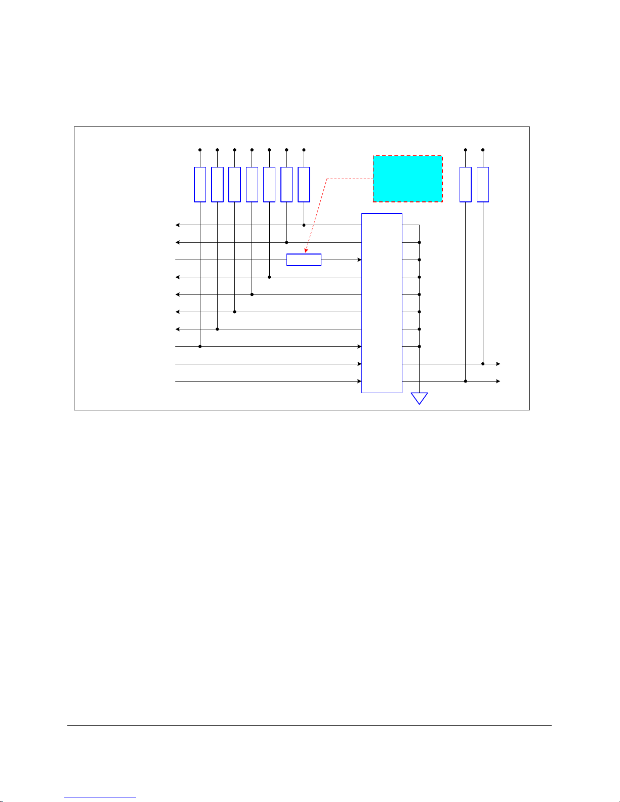
Figure A-7 shows a typical schematic of the target TAP connector with termination resistors. The
1K pull-up resistors should connect to the target Vcc supply corresponding to the interface voltage
(programmable on the PCIe-1149.1 from 1.25 to 3.3 V). Recommended resistor values are +/- 5%.
3.3V
Vcc
1K
Vcc
1K
Vcc
Vcc
1K
1K
Vcc
1K
Vcc
Vcc
The 33 ohm resistor
should be placed
1K
1K
physically close to the
device pin that drives
this signal
3.3V
1K
1K
to all bounday-scan devices
to TDI of first device
in the chain
from TDO of last device in
chain
to all bounday-scan devices
to all bounday-scan devices
to Flash Write_Strobe* pin(s)
from Flash Ready/Busy* pin(s)
for voltage measurement /
short testing
for voltage measurement /
short testing
33
Write_Strobe* / GPIO1
GPIO2
Ready_Busy* / GPIO3
UUT Power Test Point 1
UUT Power Test Point 2
TRST*
TDI
TDO
TMS
TCK
12
34
56
78
910
11 12
13 14
15 16
17 18
19 20
Figure A-7. 20-pin TAP Connector Schematic for I2C
I2C_SCL
I2C_SDA
to I2C
devices
to I2C
devices
Recommended Target Connectors A-11
Page 66

Page 67

Appendix B
Self Test Utility Software
The PCIe-1149.1 has a self test utility that can be used to test the card and make sure that it is fully
functional. Logic at the TAP connectors can read back data shifted out on TMS and TDO
synchronously with the TCK. Using these signal paths, a host can test the TAP signals all the way to
the connectors, verifying the overall functionality of the system.
Self-Test
The self-test utility is provided for off-line confidence test only and under normal circumstances
there is no need to run the self test utility software. However, if you suspect that the board is
damaged, you can run the self-test on the PCIe-1149.1 card. The self-test utility is installed on your
computer in the same folder where ScanPlus Applications (ScanPlus Runner, ScanPlus Debugger
and ScanPlus Flash Programmer) are installed. Make sure to disconnect any ScanTAP-4 TAP cables
before running the test.
Using the Windows Explorer, select and run the
appear. The program checks for the presence of a ScanTAP-4, and runs the appropriate test. Make
sure that there is no target connected to the controller or to the ScanTAP-4 before running the selftest, as they can cause the test to fail. Click on Test to run the self-test.
The program should respond with results similar to the screens shown in Figure B-1 and Figure B-2.
pci1149_t_test.exe
file. A small pop-up should
Self Test Utility Software B-1
Page 68
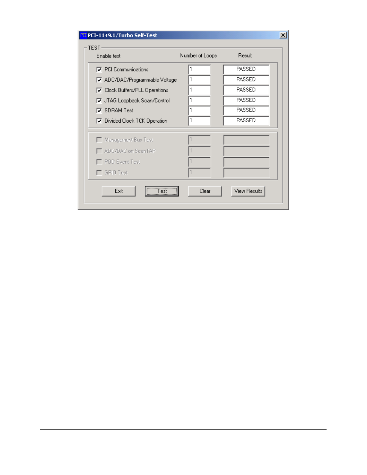
Figure B-1. Self-Test Result for the PCIe-1149.1 when the ScanTAP-4 is NOT connected
B-2 Self Test Utility Software
Page 69
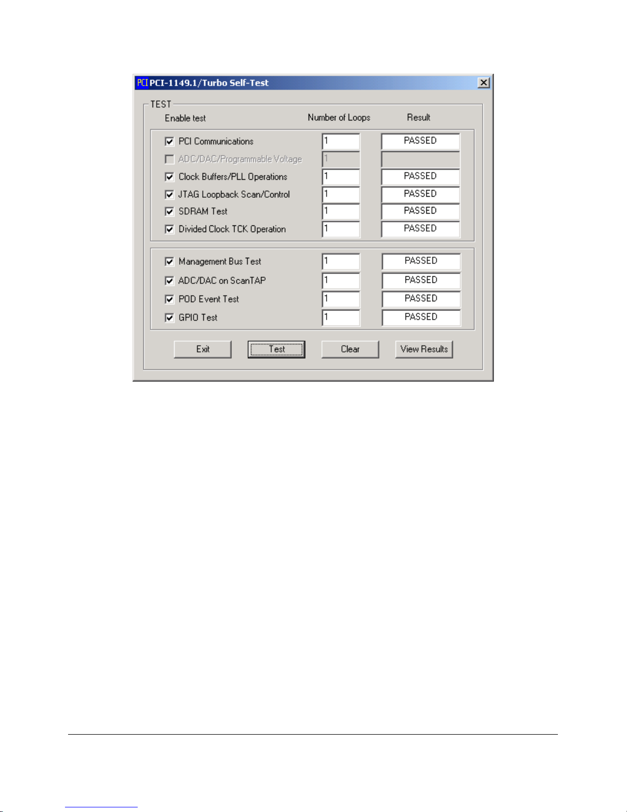
Figure B-2. Self-Test Results for the PCIe-1149.1 with the ScanTAP-4 Connected
Self Test Utility Software B-3
 Loading...