

Page 1

Functional description
T
IS-03
1
of 4
Page 2

1. SYSTEM OVERVIEW
The tire pressure monitoring system (referred as TG for Tire Guard) consists of the following
u
nits:
- Tire guard wheel unit type TIS-03 which includes an integrated pressure, temperature and
acceleration sensor and a RF transmitter.
- LF receiver unit which includes a LF receiver (not described in this document)
The TG monitors a vehicle's tire pressure while driving or stationary. An electronic unit (wheel
unit) inside each tire, mounted to the valve stem, periodically measures the actual tire pressure.
By means of RF communication, this pressure information is transmitted to the RF transmitter.
. TECHNICAL DESCRIPTION
2
Carrier frequency: 433.92 MHz
Number of channels: 1
Type of modulation: Frequency Shift Keying (FSK)
Baud rate: 9600bps
Rated Output Power: < 10mW
Antenna: Internal
Voltage supply range : 2.1 up to 3.2V
3. TYPICAL USAGE PATTERN
3.1 AVERAGE FACTOR CALCULATION (Standard 47 CFR Part 15C (periodic
intentional transmitter))
Maximum transmitting duration in whatever 100ms windows: 10.31ms
Averaging factor = 20xlog(10.31/100)=-19.73dB
Note : The time between inter frames is always higher than the 100ms FCC window.
BLOCK DIAGRAM
4.
The block diagram below shows the main electronic units of the wheel unit:
Sensor Block Diagram
FXTH870x5
(P ress ure ,
te m per a tur e,
a cce le rat io n se ns o r,
µ co nt roll er & R F
T ran s m i tte r)
C rys tal :2 6M Hz
4 3 3. 92M H z o r 3 1 5M H z
R F C IRC UI T
(T un n in g
C om pon en ts)
A NT E NN A
Le ar nin g LF co il
(1 a xe C oil @
1 25 KH z)
L I TH I UM
B A TT E RY
3 V
C R 20 5 0H R
2
of 4
Page 3

IC Block Diagram: FXTH870x5
he FXTH870x5 contains:
T
• Microcontroller with accelerometer and pressure sensor interfaces,
and RF transmitter (MCU)
• Optional ranges on pressure transducers
• Z-axis acceleration transducer
The MCU interfaces to the RF transmitter using a standard memory mapped registers. The
transducers connect to the MCU using custom analog interfaces and inter-chip bonding wires.
5. PICTURE
3
of 4
Page 4
6. LABEL
1.1. U
SA
Continental
TIS-03
FCC ID: KR5TIS-03
his device complies with Part 15 of the FCC Rules. Operation is subject to the following
T
two conditions: (1) this device may not cause harmful interference, and (2) this device
must accept any interference received, including interference that may cause undesired
operation.
Changes or modifications not expressly approved by the party responsible for
compliance could void the user's authority to operate the equipment.
1.2. CANADA
Continental
TIS-03
IC: 7812D-TIS03
Operation is subject to the following two conditions: (1) this device may not cause
harmful interference, and (2) this device must accept any interference received, including
interference that may cause undesired operation.
Changes or modifications not expressly approved by the party responsible for
compliance could void the user's authority to operate the equipment.
4
of 4
Page 5
FXTH870x6
Top and bottom view
Top view
Pin connections
24-Pin, 1-hole lid
7 x 7 QFN
20
21
22
23
24
18
PTA3
LFA
LFB
BKGD/PTA4
X0
X1
17
19
2
3
4
5
6
7
PTB1
PTA2
PTA1
8
1
RESET
10
11
12
13
14
15
V
DD
V
DDA
V
SSA
V
REG
RF
16
9
PTB0
N/C
N/C
N/C
N/C
N/C
ID Feature
on top lid
PTA0
V
SS
RFV
SS
Freescale Semiconductor Document Number: FXTH870x6
Data Sheet: Advance Information Rev. 1.5, 02/2015
An Energy-Efficient Solution by Freescale
FXTH870x6 Tire Pressure Monitor
Sensor
The FXTH870x6 family is comprised of the following functions all within the
same package.
Features
• Pressure sensor with one of two calibrated pressure ranges
— 100 - 450 kPa
— 100 - 900 kPa
• Temperature sensor
• Optional XZ- or Z-axis accelerometer with adjustable offset option
• Voltage reference measured by ADC10
• Six-channel, 10-bit analog-to-digital converter (ADC10) with two external
I/O inputs
• 8-bit MCU
— S08 Core with SIM and interrupt
— 512 RAM
— 8K FLASH (in addition to 8K providing factory firmware and trim
• Dedicated state machines to sequence routine measurement and
transmission processes for reduced power consumption
• Internal 315-/434-MHz RF transmitter
• Differential input LF detector/decoder on independent signal pins
• Seven multipurpose GPIO pins
• Real-Time Interrupt driven by LFO with interrupt intervals of
8, 16, 32, 64, 128, 256, 512 or 1024 ms
• Low-power, wakeup timer and periodic reset driven by LFO
• Watchdog timeout with selectable times and clock sources
• Two-channel general purpose timer/PWM module (TPM1)
This document contains information on a new product. Specifications and information herein
are subject to change without notice.
© 2014-2015 Freescale Semiconductor, Inc. All rights reserved.
data)
— 64-byte, low-power, parameter registers
— External crystal oscillator
— PLL-based output with fractional-n divider
— OOK and FSK modulation capability
— Programmable data rate generator
— Manchester, Bi-Phase or NRZ data encoding
— 256-bit RF data buffer variable length interrupt
— Direct access to RF transmitter from MCU for unique formats
— Low power consumption (less than 8 mA at 434 MHz, 5 dBM at
3.0 V, 25 °C)
— Four pins can be connected to optional internal pullups/pulldowns and STOP4 wakeup interrupt
— Two of seven pins can be connected to a channel on the ADC10
— Two of seven pins can be connected to a channel on the TPM1
Page 6

• Internal oscillators
Related Documentation
The FXTH870x6 device features and operations are described in a variety of reference manuals, user guides, and application
notes. To find the most-current versions of these documents:
1. Go to the Freescale homepage at:
http://www.freescale.com/
2. In the Keyword search box at the top of the page, enter the device number FXTH870x6.
— MCU bus clock of 0.5, 1, 2 and 4 MHz (1, 2, 4 and 8 MHz HFO)
— Low frequency, low power time clock (LFO) with 1 ms period
— Medium frequency, controller clock (MFO) of 8 sec period
• Low-voltage detection
• Normal temperature restart in hardware (over- or under-temperature detected by software)
ORDERING INFORMATION
Part number Accelerometer axis Package Range Code1
FXTH8705026T1 Z 2264 (7 x 7, 1-hole lid) 100-450 kPa $08
FXTH8705116T1 XZ 2264 (7 x 7, 1-hole lid) 100-450 kPa $0C
FXTH8709026T1 Z 2264 (7 x 7, 1-hole lid) 100-900 kPa $18
FXTH8709116T1 XZ 2264 (7 x 7, 1-hole lid) 100-900 kPa $1C
FXTH8709126T1 XZ Ext. Range 2264 (7 x 7, 1-hole lid) 100-900 kPa $1E
Code1 Code0
FXTH8709226T1 XZ 2264 (7 x 7, 1-hole lid) 100-900 kPa $1C Rel11
Sensors
Freescale Semiconductor, Inc. 2
FXTH870x6
Page 7

Contents
1 General Information . . . . . . . . . . . . . . . . . . . . . . . . . . . . . . . . . . . . . . . . . . . . . . . . . . . . . . . . . . . . . . . . . . . . . . . . . . . . . . 6
1.1 Overall Block Diagram . . . . . . . . . . . . . . . . . . . . . . . . . . . . . . . . . . . . . . . . . . . . . . . . . . . . . . . . . . . . . . . . . . . . . . . . 6
1.2 Multi-Chip Interface . . . . . . . . . . . . . . . . . . . . . . . . . . . . . . . . . . . . . . . . . . . . . . . . . . . . . . . . . . . . . . . . . . . . . . . . . . 6
1.3 System Clock Distribution. . . . . . . . . . . . . . . . . . . . . . . . . . . . . . . . . . . . . . . . . . . . . . . . . . . . . . . . . . . . . . . . . . . . . . 6
1.4 Reference Documents . . . . . . . . . . . . . . . . . . . . . . . . . . . . . . . . . . . . . . . . . . . . . . . . . . . . . . . . . . . . . . . . . . . . . . . . 8
2 Pins and Connections . . . . . . . . . . . . . . . . . . . . . . . . . . . . . . . . . . . . . . . . . . . . . . . . . . . . . . . . . . . . . . . . . . . . . . . . . . . . 9
2.1 Package Pinout . . . . . . . . . . . . . . . . . . . . . . . . . . . . . . . . . . . . . . . . . . . . . . . . . . . . . . . . . . . . . . . . . . . . . . . . . . . . . 9
2.2 Recommended Application. . . . . . . . . . . . . . . . . . . . . . . . . . . . . . . . . . . . . . . . . . . . . . . . . . . . . . . . . . . . . . . . . . . . . 9
2.3 Signal Properties . . . . . . . . . . . . . . . . . . . . . . . . . . . . . . . . . . . . . . . . . . . . . . . . . . . . . . . . . . . . . . . . . . . . . . . . . . . 10
3 Modes of Operation . . . . . . . . . . . . . . . . . . . . . . . . . . . . . . . . . . . . . . . . . . . . . . . . . . . . . . . . . . . . . . . . . . . . . . . . . . . . . 13
3.1 Features . . . . . . . . . . . . . . . . . . . . . . . . . . . . . . . . . . . . . . . . . . . . . . . . . . . . . . . . . . . . . . . . . . . . . . . . . . . . . . . . . . 13
3.2 RUN Mode . . . . . . . . . . . . . . . . . . . . . . . . . . . . . . . . . . . . . . . . . . . . . . . . . . . . . . . . . . . . . . . . . . . . . . . . . . . . . . . . 13
3.3 WAIT Mode. . . . . . . . . . . . . . . . . . . . . . . . . . . . . . . . . . . . . . . . . . . . . . . . . . . . . . . . . . . . . . . . . . . . . . . . . . . . . . . . 13
3.4 ACTIVE BACKGROUND Mode . . . . . . . . . . . . . . . . . . . . . . . . . . . . . . . . . . . . . . . . . . . . . . . . . . . . . . . . . . . . . . . . 13
3.5 STOP Modes . . . . . . . . . . . . . . . . . . . . . . . . . . . . . . . . . . . . . . . . . . . . . . . . . . . . . . . . . . . . . . . . . . . . . . . . . . . . . . 14
4 Memory . . . . . . . . . . . . . . . . . . . . . . . . . . . . . . . . . . . . . . . . . . . . . . . . . . . . . . . . . . . . . . . . . . . . . . . . . . . . . . . . . . . . . . . 17
4.1 MCU Memory Map. . . . . . . . . . . . . . . . . . . . . . . . . . . . . . . . . . . . . . . . . . . . . . . . . . . . . . . . . . . . . . . . . . . . . . . . . . 17
4.2 Reset and Interrupt Vectors . . . . . . . . . . . . . . . . . . . . . . . . . . . . . . . . . . . . . . . . . . . . . . . . . . . . . . . . . . . . . . . . . . . 17
4.3 MCU Register Addresses and Bit Assignments. . . . . . . . . . . . . . . . . . . . . . . . . . . . . . . . . . . . . . . . . . . . . . . . . . . . 18
4.4 High Address Registers . . . . . . . . . . . . . . . . . . . . . . . . . . . . . . . . . . . . . . . . . . . . . . . . . . . . . . . . . . . . . . . . . . . . . . 22
4.5 MCU Parameter Registers . . . . . . . . . . . . . . . . . . . . . . . . . . . . . . . . . . . . . . . . . . . . . . . . . . . . . . . . . . . . . . . . . . . . 22
4.6 MCU RAM . . . . . . . . . . . . . . . . . . . . . . . . . . . . . . . . . . . . . . . . . . . . . . . . . . . . . . . . . . . . . . . . . . . . . . . . . . . . . . . . 22
4.7 FLASH . . . . . . . . . . . . . . . . . . . . . . . . . . . . . . . . . . . . . . . . . . . . . . . . . . . . . . . . . . . . . . . . . . . . . . . . . . . . . . . . . . . 23
4.8 Security. . . . . . . . . . . . . . . . . . . . . . . . . . . . . . . . . . . . . . . . . . . . . . . . . . . . . . . . . . . . . . . . . . . . . . . . . . . . . . . . . . . 28
4.9 FLASH Registers and Control Bits . . . . . . . . . . . . . . . . . . . . . . . . . . . . . . . . . . . . . . . . . . . . . . . . . . . . . . . . . . . . . . 29
5 Reset, Interrupts and System Configuration. . . . . . . . . . . . . . . . . . . . . . . . . . . . . . . . . . . . . . . . . . . . . . . . . . . . . . . . . 33
5.1 Features . . . . . . . . . . . . . . . . . . . . . . . . . . . . . . . . . . . . . . . . . . . . . . . . . . . . . . . . . . . . . . . . . . . . . . . . . . . . . . . . . . 33
5.2 MCU Reset. . . . . . . . . . . . . . . . . . . . . . . . . . . . . . . . . . . . . . . . . . . . . . . . . . . . . . . . . . . . . . . . . . . . . . . . . . . . . . . . 33
5.3 Computer Operating Properly (COP) Watchdog . . . . . . . . . . . . . . . . . . . . . . . . . . . . . . . . . . . . . . . . . . . . . . . . . . . 33
5.4 SIM Test Register (SIMTST) . . . . . . . . . . . . . . . . . . . . . . . . . . . . . . . . . . . . . . . . . . . . . . . . . . . . . . . . . . . . . . . . . . 34
5.5 Interrupts . . . . . . . . . . . . . . . . . . . . . . . . . . . . . . . . . . . . . . . . . . . . . . . . . . . . . . . . . . . . . . . . . . . . . . . . . . . . . . . . . 35
5.6 Low-Voltage Detect (LVD) System. . . . . . . . . . . . . . . . . . . . . . . . . . . . . . . . . . . . . . . . . . . . . . . . . . . . . . . . . . . . . . 38
5.7 System Clock Control. . . . . . . . . . . . . . . . . . . . . . . . . . . . . . . . . . . . . . . . . . . . . . . . . . . . . . . . . . . . . . . . . . . . . . . . 38
5.8 Keyboard Interrupts . . . . . . . . . . . . . . . . . . . . . . . . . . . . . . . . . . . . . . . . . . . . . . . . . . . . . . . . . . . . . . . . . . . . . . . . . 38
5.9 Real Time Interrupt. . . . . . . . . . . . . . . . . . . . . . . . . . . . . . . . . . . . . . . . . . . . . . . . . . . . . . . . . . . . . . . . . . . . . . . . . . 39
5.10 Temperature Sensor and Restart System . . . . . . . . . . . . . . . . . . . . . . . . . . . . . . . . . . . . . . . . . . . . . . . . . . . . . . . . 40
5.11 Reset, Interrupt and System Control Registers And Bits . . . . . . . . . . . . . . . . . . . . . . . . . . . . . . . . . . . . . . . . . . . . . 40
5.12 System STOP Exit Status Register (SIMSES) . . . . . . . . . . . . . . . . . . . . . . . . . . . . . . . . . . . . . . . . . . . . . . . . . . . . . 45
6 General Purpose I/O. . . . . . . . . . . . . . . . . . . . . . . . . . . . . . . . . . . . . . . . . . . . . . . . . . . . . . . . . . . . . . . . . . . . . . . . . . . . . 46
6.1 Unused Pin Configuration. . . . . . . . . . . . . . . . . . . . . . . . . . . . . . . . . . . . . . . . . . . . . . . . . . . . . . . . . . . . . . . . . . . . . 48
6.2 Pin Behavior in STOP Modes. . . . . . . . . . . . . . . . . . . . . . . . . . . . . . . . . . . . . . . . . . . . . . . . . . . . . . . . . . . . . . . . . . 48
6.3 General Purpose I/O Registers . . . . . . . . . . . . . . . . . . . . . . . . . . . . . . . . . . . . . . . . . . . . . . . . . . . . . . . . . . . . . . . . 48
6.4 Port A Registers. . . . . . . . . . . . . . . . . . . . . . . . . . . . . . . . . . . . . . . . . . . . . . . . . . . . . . . . . . . . . . . . . . . . . . . . . . . . 48
6.5 Port B Registers. . . . . . . . . . . . . . . . . . . . . . . . . . . . . . . . . . . . . . . . . . . . . . . . . . . . . . . . . . . . . . . . . . . . . . . . . . . . 49
7 Keyboard Interrupt. . . . . . . . . . . . . . . . . . . . . . . . . . . . . . . . . . . . . . . . . . . . . . . . . . . . . . . . . . . . . . . . . . . . . . . . . . . . . . 51
7.1 Features . . . . . . . . . . . . . . . . . . . . . . . . . . . . . . . . . . . . . . . . . . . . . . . . . . . . . . . . . . . . . . . . . . . . . . . . . . . . . . . . . . 51
7.2 Modes of Operation . . . . . . . . . . . . . . . . . . . . . . . . . . . . . . . . . . . . . . . . . . . . . . . . . . . . . . . . . . . . . . . . . . . . . . . . . 51
7.3 Block Diagram . . . . . . . . . . . . . . . . . . . . . . . . . . . . . . . . . . . . . . . . . . . . . . . . . . . . . . . . . . . . . . . . . . . . . . . . . . . . . 51
7.4 External Signal Description . . . . . . . . . . . . . . . . . . . . . . . . . . . . . . . . . . . . . . . . . . . . . . . . . . . . . . . . . . . . . . . . . . . 51
7.5 Register Definitions . . . . . . . . . . . . . . . . . . . . . . . . . . . . . . . . . . . . . . . . . . . . . . . . . . . . .
7.6 Functional Description . . . . . . . . . . . . . . . . . . . . . . . . . . . . . . . . . . . . . . . . . . . . . . . . . . . . . . . . . . . . . . . . . . . . . . . 53
8 Central Processing Unit. . . . . . . . . . . . . . . . . . . . . . . . . . . . . . . . . . . . . . . . . . . . . . . . . . . . . . . . . . . . . . . . . . . . . . . . . . 54
8.1 Introduction. . . . . . . . . . . . . . . . . . . . . . . . . . . . . . . . . . . . . . . . . . . . . . . . . . . . . . . . . . . . . . . . . . . . . . . . . . . . . . . . 54
8.2 Features . . . . . . . . . . . . . . . . . . . . . . . . . . . . . . . . . . . . . . . . . . . . . . . . . . . . . . . . . . . . . . . . . . . . . . . . . . . . . . . . . . 54
8.3 Programmer’s Model and CPU Registers . . . . . . . . . . . . . . . . . . . . . . . . . . . . . . . . . . . . . . . . . . . . . . . . . . . . . . . . 55
8.4 Addressing Modes . . . . . . . . . . . . . . . . . . . . . . . . . . . . . . . . . . . . . . . . . . . . . . . . . . . . . . . . . . . . . . . . . . . . . . . . . . 57
8.5 Special Operations. . . . . . . . . . . . . . . . . . . . . . . . . . . . . . . . . . . . . . . . . . . . . . . . . . . . . . . . . . . . . . . . . . . . . . . . . . 58
8.6 HCS08 Instruction Set Summary . . . . . . . . . . . . . . . . . . . . . . . . . . . . . . . . . . . . . . . . . . . . . . . . . . . . . . . . . . . . . . . 59
. . . . . . . . . . . . . . . . . . . . 52
FXTH870x6
Sensors
Freescale Semiconductor, Inc. 3
Page 8

9 Timer Pulse-Width Module. . . . . . . . . . . . . . . . . . . . . . . . . . . . . . . . . . . . . . . . . . . . . . . . . . . . . . . . . . . . . . . . . . . . . . . . 70
9.1 Features . . . . . . . . . . . . . . . . . . . . . . . . . . . . . . . . . . . . . . . . . . . . . . . . . . . . . . . . . . . . . . . . . . . . . . . . . . . . . . . . . . 70
9.2 TPM1 Configuration Information. . . . . . . . . . . . . . . . . . . . . . . . . . . . . . . . . . . . . . . . . . . . . . . . . . . . . . . . . . . . . . . . 70
9.3 External Signal Description . . . . . . . . . . . . . . . . . . . . . . . . . . . . . . . . . . . . . . . . . . . . . . . . . . . . . . . . . . . . . . . . . . . 71
9.4 Register Definition . . . . . . . . . . . . . . . . . . . . . . . . . . . . . . . . . . . . . . . . . . . . . . . . . . . . . . . . . . . . . . . . . . . . . . . . . . 72
9.5 Functional Description . . . . . . . . . . . . . . . . . . . . . . . . . . . . . . . . . . . . . . . . . . . . . . . . . . . . . . . . . . . . . . . . . . . . . . . 77
9.6 TPM1 Interrupts . . . . . . . . . . . . . . . . . . . . . . . . . . . . . . . . . . . . . . . . . . . . . . . . . . . . . . . . . . . . . . . . . . . . . . . . . . . . 80
10 .Other MCU Resources. . . . . . . . . . . . . . . . . . . . . . . . . . . . . . . . . . . . . . . . . . . . . . . . . . . . . . . . . . . . . . . . . . . . . . . . . . . 82
10.1 Pressure Measurement . . . . . . . . . . . . . . . . . . . . . . . . . . . . . . . . . . . . . . . . . . . . . . . . . . . . . . . . . . . . . . . . . . . . . . 82
10.2 Temperature Measurements . . . . . . . . . . . . . . . . . . . . . . . . . . . . . . . . . . . . . . . . . . . . . . . . . . . . . . . . . . . . . . . . . . 83
10.3 Voltage Measurements. . . . . . . . . . . . . . . . . . . . . . . . . . . . . . . . . . . . . . . . . . . . . . . . . . . . . . . . . . . . . . . . . . . . . . . 83
10.4 Optional Acceleration Measurements. . . . . . . . . . . . . . . . . . . . . . . . . . . . . . . . . . . . . . . . . . . . . . . . . . . . . . . . . . . . 83
10.5 Optional Battery Condition Check . . . . . . . . . . . . . . . . . . . . . . . . . . . . . . . . . . . . . . . . . . . . . . . . . . . . . . . . . . . . . . 83
10.6 Measurement Firmware . . . . . . . . . . . . . . . . . . . . . . . . . . . . . . . . . . . . . . . . . . . . . . . . . . . . . . . . . . . . . . . . . . . . . . 85
10.7 Thermal Shutdown . . . . . . . . . . . . . . . . . . . . . . . . . . . . . . . . . . . . . . . . . . . . . . . . . . . . . . . . . . . . . . . . . . . . . . . . . . 87
11 Periodic Wakeup Timer . . . . . . . . . . . . . . . . . . . . . . . . . . . . . . . . . . . . . . . . . . . . . . . . . . . . . . . . . . . . . . . . . . . . . . . . . . 89
11.1 Block Diagram . . . . . . . . . . . . . . . . . . . . . . . . . . . . . . . . . . . . . . . . . . . . . . . . . . . . . . . . . . . . . . . . . . . . . . . . . . . . . 89
11.2 Wakeup Divider Register - PWUDIV . . . . . . . . . . . . . . . . . . . . . . . . . . . . . . . . . . . . . . . . . . . . . . . . . . . . . . . . . . . . 90
11.3 PWU Control/Status Register 0 - PWUCS0. . . . . . . . . . . . . . . . . . . . . . . . . . . . . . . . . . . . . . . . . . . . . . . . . . . . . . . 90
11.4 PWU Control/Status Register 1 - PWUCS1. . . . . . . . . . . . . . . . . . . . . . . . . . . . . . . . . . . . . . . . . . . . . . . . . . . . . . . 91
11.5 PWU Wakeup Status Register - PWUS . . . . . . . . . . . . . . . . . . . . . . . . . . . . . . . . . . . . . . . . . . . . . . . . . . . . . . . . . . 92
11.6 Functional Modes. . . . . . . . . . . . . . . . . . . . . . . . . . . . . . . . . . . . . . . . . . . . . . . . . . . . . . . . . . . . . . . . . . . . . . . . . . . 92
12 LF Receiver. . . . . . . . . . . . . . . . . . . . . . . . . . . . . . . . . . . . . . . . . . . . . . . . . . . . . . . . . . . . . . . . . . . . . . . . . . . . . . . . . . . . 93
12.1 Features . . . . . . . . . . . . . . . . . . . . . . . . . . . . . . . . . . . . . . . . . . . . . . . . . . . . . . . . . . . . . . . . . . . . . . . . . . . . . . . . . . 94
12.2 Modes of Operation . . . . . . . . . . . . . . . . . . . . . . . . . . . . . . . . . . . . . . . . . . . . . . . . . . . . . . . . . . . . . . . . . . . . . . . . . 94
12.3 Power Management . . . . . . . . . . . . . . . . . . . . . . . . . . . . . . . . . . . . . . . . . . . . . . . . . . . . . . . . . . . . . . . . . . . . . . . . . 94
12.4 Input Amplifier. . . . . . . . . . . . . . . . . . . . . . . . . . . . . . . . . . . . . . . . . . . . . . . . . . . . . . . . . . . . . . . . . . . . . . . . . . . . . . 95
12.5 LFR Data Mode States. . . . . . . . . . . . . . . . . . . . . . . . . . . . . . . . . . . . . . . . . . . . . . . . . . . . . . . . . . . . . . . . . . . . . . . 95
12.6 Carrier Detect. . . . . . . . . . . . . . . . . . . . . . . . . . . . . . . . . . . . . . . . . . . . . . . . . . . . . . . . . . . . . . . . . . . . . . . . . . . . . . 95
12.7 Auto-Zero Sequence . . . . . . . . . . . . . . . . . . . . . . . . . . . . . . . . . . . . . . . . . . . . . . . . . . . . . . . . . . . . . . . . . . . . . . . . 97
12.8 Data Recovery . . . . . . . . . . . . . . . . . . . . . . . . . . . . . . . . . . . . . . . . . . . . . . . . . . . . . . . . . . . . . . . . . . . . . . . . . . . . . 97
12.9 Data Clock Recovery and Synchronization . . . . . . . . . . . . . . . . . . . . . . . . . . . . . . . . . . . . . . . . . . . . . . . . . . . . . . . 97
12.10 Manchester Decode . . . . . . . . . . . . . . . . . . . . . . . . . . . . . . . . . . . . . . . . . . . . . . . . . . . . . . . . . . . . . . . . . . . . . . . . . 97
12.11 Duty-Cycle For Data Mode. . . . . . . . . . . . . . . . . . . . . . . . . . . . . . . . . . . . . . . . . . . . . . . . . . . . . . . . . . . . . . . . . . . . 98
12.12 Input Signal Envelope. . . . . . . . . . . . . . . . . . . . . . . . . . . . . . . . . . . . . . . . . . . . . . . . . . . . . . . . . . . . . . . . . . . . . . . . 99
12.13 Telegram Verification . . . . . . . . . . . . . . . . . . . . . . . . . . . . . . . . . . . . . . . . . . . . . . . . . . . . . . . . . . . . . . . . . . . . . . . 100
12.14 Error Detection and Handling. . . . . . . . . . . . . . . . . . . . . . . . . . . . . . . . . . . . . . . . . . . . . . . . . . . . . . . . . . . . . . . . . 101
12.15 Continuous ON Mode. . . . . . . . . . . . . . . . . . . . . . . . . . . . . . . . . . . . . . . . . . . . . . . . . . . . . . . . . . . . . . . . . . . . . . . 101
12.16 Initialization Information . . . . . . . . . . . . . . . . . . . . . . . . . . . . . . . . . . . . . . . . . . . . . . . . . . . . . . . . . . . . . . . . . . . . . 101
12.17 LFR Register Definition . . . . . . . . . . . . . . . . . . . . . . . . . . . . . . . . . . . . . . . . . . . . . . . . . . . . . . . . . . . . . . . . . . . . . 102
13 RF Module . . . . . . . . . . . . . . . . . . . . . . . . . . . . . . . . . . . . . . . . . . . . . . . . . . . . . . . . . . . . . . . . . . . . . . . . . . . . . . . . . . . . 113
13.1 RF Data Modes . . . . . . . . . . . . . . . . . . . . . . . . . . . . . . . . . . . . . . . . . . . . . . . . . . . . . . . . . . . . . . . . . . . . . . . . . . . 113
13.2 RF Output Buffer Data Frame . . . . . . . . . . . . . . . . . . . . . . . . . . . . . . . . . . . . . . . . . . . . . . . . . . . . . . . . . . . . . . . . 114
13.3 Transmission Randomization. . . . . . . . . . . . . . . . . . . . . . . . . . . . . . . . . . . . . . . . . . . . . . . . . . . . . . . . . . . . . . . . . 116
13.4 RFM in STOP1 Mode. . . . . . . . . . . . . . . . . . . . . . . . . . . . . . . . . . . . . . . . . . . . . . . . . . . . . . . . . . . . . . . . . . . . . . . 119
13.5 Data Encoding . . . . . . . . . . . . . . . . . . . . . . . . . . . . . . . . . . . . . . . . . . . . . . . . . . . . . . . . . . . . . . . . . . . . . . . . . . . . 119
13.6 RF Output Stage. . . . . . . . . . . . . . . . . . . . . . . . . . . . . . . . . . . . . . . . . . . . . . . . . . . . . . .
13.7 RF Interrupt . . . . . . . . . . . . . . . . . . . . . . . . . . . . . . . . . . . . . . . . . . . . . . . . . . . . . . . . . . . . . . . . . . . . . . . . . . . . . . 122
13.8 Datagram Transmission Times. . . . . . . . . . . . . . . . . . . . . . . . . . . . . . . . . . . . . . . . . . . . . . . . . . . . . . . . . . . . . . . . 122
13.9 RFM Registers . . . . . . . . . . . . . . . . . . . . . . . . . . . . . . . . . . . . . . . . . . . . . . . . . . . . . . . . . . . . . . . . . . . . . . . . . . . . 123
13.10 RFM Control Register 1 - RFCR1. . . . . . . . . . . . . . . . . . . . . . . . . . . . . . . . . . . . . . . . . . . . . . . . . . . . . . . . . . . . . . 123
13.11 RFM Control Register 2 - RFCR2. . . . . . . . . . . . . . . . . . . . . . . . . . . . . . . . . . . . . . . . . . . . . . . . . . . . . . . . . . . . . . 124
13.12 RFM Control Register 3 - RFCR3. . . . . . . . . . . . . . . . . . . . . . . . . . . . . . . . . . . . . . . . . . . . . . . . . . . . . . . . . . . . . . 127
13.13 RFM Control Register 4 - RFCR4. . . . . . . . . . . . . . . . . . . . . . . . . . . . . . . . . . . . . . . . . . . . . . . . . . . . . . . . . . . . . . 128
13.14 RFM Control Register 5 - RFCR5. . . . . . . . . . . . . . . . . . . . . . . . . . . . . . . . . . . . . . . . . . . . . . . . . . . . . . . . . . . . . . 128
13.15 RFM Control Register 6 - RFCR6. . . . . . . . . . . . . . . . . . . . . . . . . . . . . . . . . . . . . . . . . . . . . . . . . . . . . . . . . . . . . . 129
13.16 RFM Control Register 7 - RFCR7. . . . . . . . . . . . . . . . . . . . . . . . . . . . . . . . . . . . . . . . . . . . . . . . . . . . . . . . . . . . . . 129
13.17 PLL Control Registers A- PLLCR[1:0], RPAGE = 0 . . . . . . . . . . . . . . . . . . . . . . . . . . . . . . . . . . . . . . . . . . . . . . . . 130
13.18 PLL Control Registers B- PLLCR[3:2], RPAGE = 0 . . . . . . . . . . . . . . . . . . . . . . . . . . . . . . . . . . . . . . . . . . . . . . . . 131
13.19 EPR Register - EPR (RPAGE = 1). . . . . . . . . . . . . . . . . . . . . . . . . . . . . . . . . . . . . . . . . . . . . . . . . . . . . . . . . . . . . 132
13.20 RF DATA Registers - RFD[31:0] . . . . . . . . . . . . . . . . . . . . . . . . . . . . . . . . . . . . . . . . . . . . . . . . . . . . . . . . . . . . . . 133
13.21 VCO Calibration Machine. . . . . . . . . . . . . . . . . . . . . . . . . . . . . . . . . . . . . . . . . . . . . . . . . . . . . . . . . . . . . . . . . . . . 134
. . . . . . . . . . . . . . . . . . . . 121
FXTH870x6
Sensors
4 Freescale Semiconductor, Inc.
Page 9

14 Firmware . . . . . . . . . . . . . . . . . . . . . . . . . . . . . . . . . . . . . . . . . . . . . . . . . . . . . . . . . . . . . . . . . . . . . . . . . . . . . . . . . . . . . 135
14.1 Software Jump Table . . . . . . . . . . . . . . . . . . . . . . . . . . . . . . . . . . . . . . . . . . . . . . . . . . . . . . . . . . . . . . . . . . . . . . . 135
14.2 Function Documentation. . . . . . . . . . . . . . . . . . . . . . . . . . . . . . . . . . . . . . . . . . . . . . . . . . . . . . . . . . . . . . . . . . . . . 135
14.3 Memory Resource Usage. . . . . . . . . . . . . . . . . . . . . . . . . . . . . . . . . . . . . . . . . . . . . . . . . . . . . . . . . . . . . . . . . . . . 140
15 Development Support . . . . . . . . . . . . . . . . . . . . . . . . . . . . . . . . . . . . . . . . . . . . . . . . . . . . . . . . . . . . . . . . . . . . . . . . . . 141
15.1 Introduction. . . . . . . . . . . . . . . . . . . . . . . . . . . . . . . . . . . . . . . . . . . . . . . . . . . . . . . . . . . . . . . . . . . . . . . . . . . . . . . 141
15.2 Background Debug Controller (BDC). . . . . . . . . . . . . . . . . . . . . . . . . . . . . . . . . . . . . . . . . . . . . . . . . . . . . . . . . . . 141
15.3 Register Definition . . . . . . . . . . . . . . . . . . . . . . . . . . . . . . . . . . . . . . . . . . . . . . . . . . . . . . . . . . . . . . . . . . . . . . . . . 146
16 Battery Charge Consumption Modeling. . . . . . . . . . . . . . . . . . . . . . . . . . . . . . . . . . . . . . . . . . . . . . . . . . . . . . . . . . . . 149
16.1 Standby Current. . . . . . . . . . . . . . . . . . . . . . . . . . . . . . . . . . . . . . . . . . . . . . . . . . . . . . . . . . . . . . . . . . . . . . . . . . . 149
16.2 Measurement Events . . . . . . . . . . . . . . . . . . . . . . . . . . . . . . . . . . . . . . . . . . . . . . . . . . . . . . . . . . . . . . . . . . . . . . . 149
16.3 Transmission Events . . . . . . . . . . . . . . . . . . . . . . . . . . . . . . . . . . . . . . . . . . . . . . . . . . . . . . . . . . . . . . . . . . . . . . . 149
16.4 Total Consumption. . . . . . . . . . . . . . . . . . . . . . . . . . . . . . . . . . . . . . . . . . . . . . . . . . . . . . . . . . . . . . . . . . . . . . . . . 149
17 Electrical Specifications . . . . . . . . . . . . . . . . . . . . . . . . . . . . . . . . . . . . . . . . . . . . . . . . . . . . . . . . . . . . . . . . . . . . . . . . 150
17.1 Maximum Ratings. . . . . . . . . . . . . . . . . . . . . . . . . . . . . . . . . . . . . . . . . . . . . . . . . . . . . . . . . . . . . . . . . . . . . . . . . . 150
17.2 Operating Range . . . . . . . . . . . . . . . . . . . . . . . . . . . . . . . . . . . . . . . . . . . . . . . . . . . . . . . . . . . . . . . . . . . . . . . . . . 150
17.3 Electrical Characteristics . . . . . . . . . . . . . . . . . . . . . . . . . . . . . . . . . . . . . . . . . . . . . . . . . . . . . . . . . . . . . . . . . . . . 151
17.4 Power Consumption (MCU) . . . . . . . . . . . . . . . . . . . . . . . . . . . . . . . . . . . . . . . . . . . . . . . . . . . . . . . . . . . . . . . . . . 152
17.5 Control Timing . . . . . . . . . . . . . . . . . . . . . . . . . . . . . . . . . . . . . . . . . . . . . . . . . . . . . . . . . . . . . . . . . . . . . . . . . . . . 153
17.6 Voltage Measurement Characteristics . . . . . . . . . . . . . . . . . . . . . . . . . . . . . . . . . . . . . . . . . . . . . . . . . . . . . . . . . . 154
17.7 Temperature Measurement Characteristics. . . . . . . . . . . . . . . . . . . . . . . . . . . . . . . . . . . . . . . . . . . . . . . . . . . . . . 155
17.8 Pressure Measurement Characteristic (100 to 450 kPa ranges) . . . . . . . . . . . . . . . . . . . . . . . . . . . . . . . . . . . . . . 156
17.9 Pressure Measurement Characteristic (100 to 900 kPa Ranges) . . . . . . . . . . . . . . . . . . . . . . . . . . . . . . . . . . . . . 157
17.10 Optional Acceleration Sensor Characteristics . . . . . . . . . . . . . . . . . . . . . . . . . . . . . . . . . . . . . . . . . . . . . . . . . . . . 158
17.11 LFR Sensitivity . . . . . . . . . . . . . . . . . . . . . . . . . . . . . . . . . . . . . . . . . . . . . . . . . . . . . . . . . . . . . . . . . . . . . . . . . . . . 161
17.12 LFR Characteristics . . . . . . . . . . . . . . . . . . . . . . . . . . . . . . . . . . . . . . . . . . . . . . . . . . . . . . . . . . . . . . . . . . . . . . . . 162
17.13 LFR Power Consumption . . . . . . . . . . . . . . . . . . . . . . . . . . . . . . . . . . . . . . . . . . . . . . . . . . . . . . . . . . . . . . . . . . . . 162
17.14 RF Output Stage. . . . . . . . . . . . . . . . . . . . . . . . . . . . . . . . . . . . . . . . . . . . . . . . . . . . . . . . . . . . . . . . . . . . . . . . . . . 164
17.15 Power Consumption RF Transmissions . . . . . . . . . . . . . . . . . . . . . . . . . . . . . . . . . . . . . . . . . . . . . . . . . . . . . . . . . 166
18 Mechanical Specifications. . . . . . . . . . . . . . . . . . . . . . . . . . . . . . . . . . . . . . . . . . . . . . . . . . . . . . . . . . . . . . . . . . . . . . . 168
18.1 Maximum Ratings. . . . . . . . . . . . . . . . . . . . . . . . . . . . . . . . . . . . . . . . . . . . . . . . . . . . . . . . . . . . . . . . . . . . . . . . . . 168
18.2 Media Compatibility . . . . . . . . . . . . . . . . . . . . . . . . . . . . . . . . . . . . . . . . . . . . . . . . . . . . . . . . . . . . . . . . . . . . . . . . 168
18.3 Mounting Recommendations . . . . . . . . . . . . . . . . . . . . . . . . . . . . . . . . . . . . . . . . . . . . . . . . . . . . . . . . . . . . . . . . . 168
19 Package Outline . . . . . . . . . . . . . . . . . . . . . . . . . . . . . . . . . . . . . . . . . . . . . . . . . . . . . . . . . . . . . . . . . . . . . . . . . . . . . . . 170
20 Revision History . . . . . . . . . . . . . . . . . . . . . . . . . . . . . . . . . . . . . . . . . . . . . . . . . . . . . . . . . . . . . . . . . . . . . . . . . . . . . . . 174
FXTH870x6
Sensors
Freescale Semiconductor, Inc. 5
Page 10

1 General Information
1.1 Overall Block Diagram
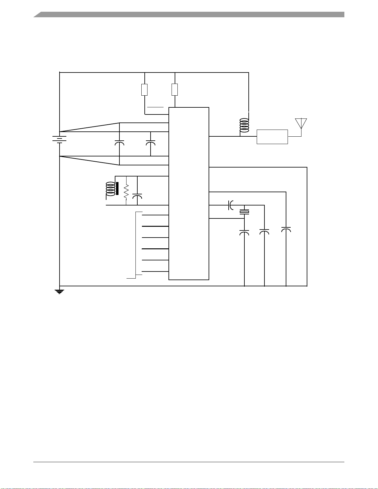
The block diagram of the FXTH870x6 is shown in Figure 1. This diagram covers all the main blocks mentioned above and their
main signal interactions. Power management controls and bus control signals are not shown in this block diagram for clarity.
1.2 Multi-Chip Interface
The FXTH870x6 contains two to three devices using the best process technology for each.
• Microcontroller with accelerometer and pressure sensor interfaces, and RF transmitter (MCU)
• Optional ranges on pressure transducers
• Optional XZ- or Z-axis acceleration transducer
As shown in Figure 1 the MCU interfaces to the RF transmitter using a standard memory mapped registers. The transducers
connect to the MCU using custom analog interfaces and inter-chip bonding wires.
1.3 System Clock Distribution
The various clock sources and their distribution are shown in Figure 2. All clock sources except the low frequency oscillator, LFO,
can be turned off by software control in order to conserve power.
FXTH870x6
Sensors
6 Freescale Semiconductor, Inc.
Page 11
8K USER
FLASH
MEMORY
RAM
MEMORY
512
TPM1
TIMER/PWM
2-CHAN
LVD
RTI
TIMER
MCU CORE
S08
AV
DD
TEMP
AV
DD
AV
SS
TEMP
SENSOR
PRESS
SENSOR
BANDGAP
REF
LFA
PTA1
ADC10
10-BIT
6-CHAN
TEMP
BKGD
/
LFB
64 Byte
PARAMETER
REGISTER
DATA
ENCODE
BIT
RATE
256-BIT
DATA
BUFFER
RF
AMP
VCO/PLL
FRACTL
DIVIDER
XTAL
OSC
XI
XO
RF
MCU
TRANSDUCERS
VOLT
REG
RESTART
OSC
GEN
PWU
TIMER
MFO
8 Sec
RESET
LF
RECVR
D
X
V
SENS
V
TP
V
0
LFO
1 ms
LFI
SMI
Z
HFO
1, 2, 4 or 8
MHz
GP
I/O
KEY
KBI
BOARD
WAKEUP
MFO
8K
FIRMWARE
MEMORY
PTA0
P
SENSOR MEASUREMENT
(SMI)
RF CONTROLLER
INTERF A CE
LFO
(LFR)
RFM
V
REG
PTA2
V
DD
V
DD
V
SS
RV
SS
PTA3
V
1
V
2
RF LVD
AV
DD
RFV
DD
V
REG
PTB0
PTB1
PTA4
XZ
XZ
ACCEL
(OPTION)
Z
ACCEL
(OPTION)
Figure 1. FXTH870x6 Overall Block Diagram
FXTH870x6
Sensors
Freescale Semiconductor, Inc. 7
Page 12
RTI
SYSTEM
CONTROL
LOGIC
2
HFO OSC
1, 2, 4,
f
OSC
f
BUS
CPU
BDC
TPM1
RAM FLASH
LFR
ADC10
MFO
OSC
8 Sec
PWU
CLSA, CLKSB
f
LFO
(1 kHz)
XTL
OSC
26 MHz
XI XO
PLL VCO
BIT
RATE
DATA
BUFFER
PRESSURE
SENSOR
TRANSDUCERS
MCU
RTICLKS
PAR
REG
f
MFO
f
XCO
GEN
D
X
(500 kHz)
LFO
OSC
1 mS
PERIOD
SENSOR MEASUREMENT
INTERFACE
ADC10
CLOCK
ADCCLK ADC10
BUSCLKS[1:0]
WATCH
DOG
COPCLKS
Z-AXIS
SENSOR
LF
4 kbps
(125 kHz)
RF STATE
MACHINE
LFRO
OSCILL
8
TCLKDIV
LFOSEL
f
MFO
PTA3
PTA2
f
LFO
(1 kHz)
CH0 CH1
RANDOM
(0 - 1 MHz)
RANDOM
(0 - 1 MHz)
RF
OUT
41.67 kHz
Sampling
41.67 kHz
Sampling
and 8 MHz
X-AXIS
SENSOR
41.67 kHz
Sampling
Figure 2. Clock Distribution
1.4 Reference Documents
The FXTH870x6 utilizes the standard product MC9S08 CPU core. The user can obtain further detail on the full capabilities of this
core by referring to the HCS08 Family Reference Manual (HCS08RMV1).
FXTH870x6
8 Freescale Semiconductor, Inc.
Sensors
Page 13
2 Pins and Connections
20
21
22
23
24
18
PTA3
LFA
LFB
BKGD/PTA4
X0
X1
17
19
2
3
4
5
6
7
PTB1
PTA2
PTA1
8
1
RESET
10
11
12
13
14
15
V
DD
V
DDA
V
SSA
V
REG
RF
16
9
PTB0
N/C
N/C
N/C
N/C
N/C
ID Feature
on top lid
PTA0
V
SS
RFV
SS
N/C = No Connect: Do not connect PCB pads to signal traces, power/ground or multi-layer via.
Top View
BKGD/PTA4
X-AXIS
ORIENTATION
+X
-X
Y-AXIS
ORIENTATION
+Y
-Y
Side View
Pressure
Port
POSITIVE ACCELERATION MOVES MASS
IN +Z DIRECTION (VALUE INCREASES)
Z-AXIS
ORIENTATION
+Z
-Z
This section describes the pin layout and general function of each pin.
2.1 Package Pinout
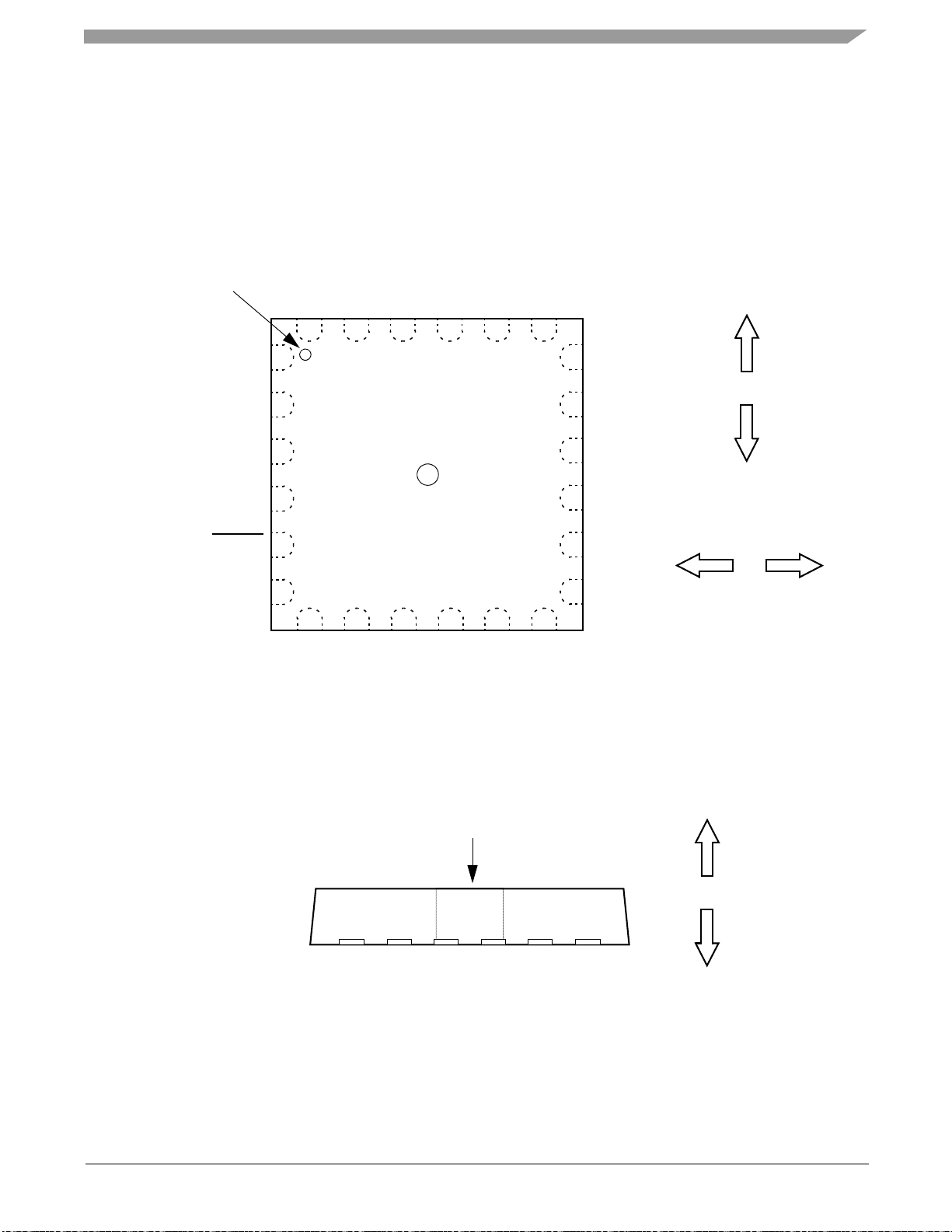
The pinout for the FXTH870x6 device QFN package is shown in Figure 3 for the orientation of the pressure port up. The
orientation of the internal Z-axis accelerometer is shown in Figure 4.
Figure 3. FXTH870x6 QFN Package Pinout
2.2 Recommended Application
Example of a simple OOK/FSK tire pressure monitors using the internal PLL-based RF output stage is shown in Figure 5. Any of
the PTA[3:0] pins can also be used as general purpose I/O pins. Any of the PTA[3:0] pins that are not used in the application
should be handled as described in Section 6.1.
Sensors
Freescale Semiconductor, Inc. 9
Figure 4. FXTH870x6 QFN Optional Z-axis Accelerometer Orientation
FXTH870x6
Page 14
2.3 Signal Properties
FXTH870xxx
0.1 µF
V
DD
V
SS
3.0 V
BATTERY
LF
COIL
XTAL
RF
RV
SS
XI
XO
C1
ANT
L1
BKGD/PTA4
LFA
LFB
PTA1
RESET
GENERAL
PURPOSE I/O
PTA0
PTA2
AV
DD
AV
SS
V
REG
470 nF
0.1 µF
PTA3
MATCHING
NETWORK
C2
C3
C2, C3, C4
optimized
for crystal
C5
C4*
R2
R3
R2 and R3, <10 k
recommended for
highest EMC resistance
R1
PTB0
PTB1
L1 and matching network
optimized for specific PWB and
antenna layout. Recommend
0603 minimum size for L1 and
other matching network inductors
for maximum efficiency.
C1 and R1 optimized
for coil used, but
recommended
RC < 15.3 sec.
The device C
4
, although drawn here as a capacitor, may be any type of passive component(s) sufficient to block
or reduce unwanted external radiated signals from corrupting the crystal oscillator circuit: PCB traces for the LFA
/ LFB, A V
DD
/ VDD, and VSS / A VSS pins and bypass capacitors should be minimized to reduce unw anted external
radiated signals from corrupting the power input circuits.
The following sections describe the general function of each pin.
2.3.1 VDD and VSS Pins
The digital circuits operate from a single power supply connected to the FXTH870x6 through the VDD and VSS pins. VDD is the
positive supply and V
locally decoupled as shown in Figure 6.
Care should be taken to reduce measurement signal noise by separating the V
connection such that each metal trace does not share any load currents with other external devices as shown in Figure 6.
2.3.2 AVDD and AVSS Pins
is the ground. The conductors to the power supply should be connected to the VDD and VSS pins and
SS
Figure 5. FXTH870x6 Example Application
The analog circuits operate from a single power supply connected to the FXTH870x6 through the AVDD and AVSS pins. AVDD is
the positive supply and AVSS is the ground. The conductors to the power supply should be connected to the AVDD and AVSS pins
and locally decoupled as shown in Figure 6.
, VSS, A VDD, A VSS and RVSS pins using a “star”
DD
FXTH870x6
10 Freescale Semiconductor, Inc.
Sensors
Page 15
Care should be taken to reduce measurement signal noise by separating the V
0.1 µF
FXTH870xxx
V
DD
V
SS
to other
Battery
I
DD
I
LOAD
Bypass capacitors
closely coupled to
the package pins
FXTH870xxx and Other Load Currents
star connected to battery terminals
loads
0.1 µF
AV
DD
AV
SS
RV
SS
The decoupling devices, although
drawn here as 0.1 F capacitors,
may be any type of passive component(s)
sufficient to block or reduce unwanted
external radiated signals from corrupting
the power input protection circuits;
application tuning may be required.
connection such that each metal trace does not share any load currents with other external devices as shown in Figure 6.
Figure 6. Recommended Power Supply Connections
, VSS, A VDD, A VSS and RVSS pins using a “star”
DD
2.3.3 V
The internal regulator for the analog circuits requires an external stabilization capacitor to AVSS.
REG
Pin
2.3.4 RVSS Pin
Power in the RF output amplifier is returned to the supply through the RVSS pin. This conductor should be connected to the power
supply as shown in Figure 6 using a “star” connection such that each metal trace does not share any load currents with other
supply pins.
2.3.5 RF Pin
The RF pin is the RF energy data supplied by the FXTH870x6 to an external antenna.
2.3.6 XO, XI Pins
The XO and XI pins are for an external crystal to be used by the internal PLL for creating the carrier frequencies and data rates
for the RF pin.
2.3.7 LF[A:B] Pins
The LF[A:B] pins can be used by the LF receiver (LFR) as one differential input channel for sensing low level signals from an
external low frequency (LF) coil. The external LF coil should be connected between the LFA and the LFB pins.
Signaling into the LFR pins can place the FXTH870x6 into various diagnostic or operational modes. The LFR is comprised of the
detector and the decoder.
Each LF[A:B] pin will always have an impedance of approximately 500 k to V
pins are used by the LFR when the LFEN con tro l b it is set and are not functional when the LFEN control bit is clear.
2.3.8 PTA[1:0] Pins
The PTA[1:0] pins are general purpose I/O pins. These two pins can be configured as normal bidirectional I/O pins with
programmable pullup or pulldown devices and/or wakeup interrupt capability; or one or both can be connected to the two input
channels of the A/D converter module. The pulldown devices can only be activated if the wakeup interrupt capability is enabled.
User software must configure the general purpose I/O pins so that they do not result in “floating” inputs as described in
Section 6.1. PTA[1:02] map to keyboard Interrupt function bits [1:0].
Sensors
Freescale Semiconductor, Inc. 11
due to the LFR input circuitry. The LFA/LFB
SS
FXTH870x6
Page 16
2.3.9 PTA[3:2] Pins
RESET
0.7 V
DD
0.3 V
DD
> 100 nsec
Reset
Initiated
The PTA[3:2] pins are general purpose I/O pin. These two pins can be configured as normal bidirectional I/O pin with
programmable pullup or pulldown devices and/or wakeup interrupt capability; or one or both can be connected to the two input
channels of the Timer Pulse Width (TPM1) module. The pulldown devices can only be activated if the wakeup interrupt capability
is enabled. User software must configure the general purpose I/O pins so that they do not result in “floating” inputs as described
in Section 6.1. PTA[3:2] map to keyboard Interrupt function bits [3:2].
2.3.10 BKGD/PTA4 Pin
The BKGD/PTA4 pin is used to place the FXTH870x6 in the BACKGROUND DEBUG mode (BDM) to evaluate MCU code and
to also transfer data to/from the internal memories. If the BKGD/PT A4 pin is held low when the FXTH870x6 comes out of a poweron reset the device will go into the ACTIVE BACKGROUND DEBUG mode (BDM).
The BKGD/PTA4 pin has an internal pullup device and can connected to V
BDM operation after the device as been soldered into the PWB. If in-circuit BDM is desired the BKGD/PTA4 pin can be left
unconnected, but should be connected to VDD through a low impedance resistor (< 10 k) which can be over-driven by an
external signal. This low impedance resistor reduces the possibility of getting into the debug mode in the application due to an
EMC event.
in the application unless there is a need to enter
DD
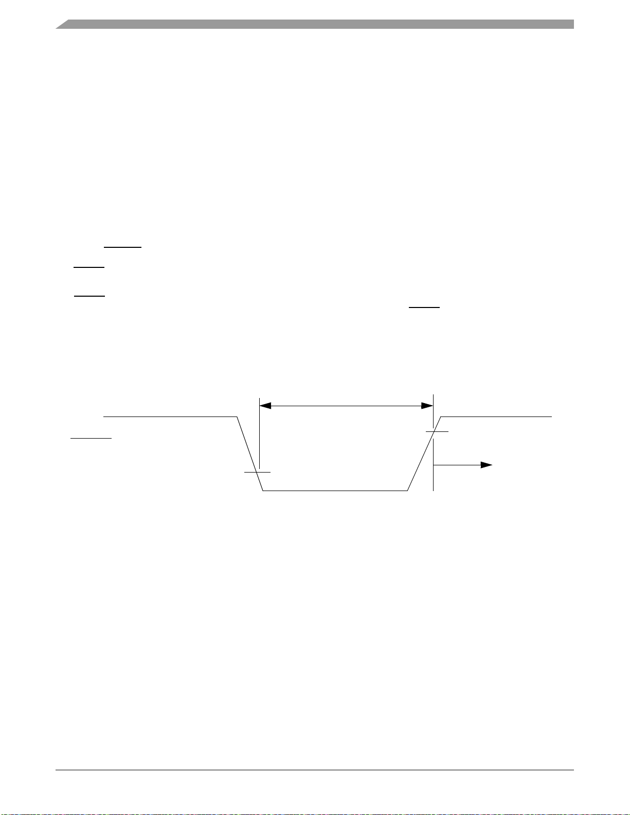
2.3.11 RESET Pin
The RESET pin is used for test and establishing the BDM condition and providing the programming voltage source to the internal
FLASH memory. This pin can also be used to direct to the MCU to the reset vector as described in Section 5.2.
The RESET
operation after the device as been soldered to the PWB. If in-circuit BDM is desired the RESET
should be connected to VDD through a low impedance resistor (< 10 k) which can be over-driven by an external signal. This
low impedance resistor reduces the possibility of getting into the debug mode in the application due to an EMC event.
Activation of the external reset function occurs when the voltage on the RESET pin goes below 0.3 x V
before rising above 0.7 x VDD as shown in Figure 7.
pin has an internal pullup device and can connected to VDD in the application unless there is a need to enter BDM
pin can be left unconnected; but
for at least 100 nsec
DD
Figure 7. RESET Pin Timing
2.3.12 PTB[1:0] Pins
The PTB[1:0] pins are general purpose I/O pins. These two pins can be configured as nominal bidirectional I/O pins with
programmable pullup. User software must configure the general purpose I/O pins so that they do not result in “floating” inputs as
described in Section 6.1
FXTH870x6
12 Freescale Semiconductor, Inc.
Sensors
Page 17

3 Modes of Operation
The operating modes of the FXTH870x6 are described in this section. Entry into each mode, exit from each mode, and
functionality while in each of the modes are described.
3.1 Features
• ACTIVE BACKGROUND DEBUG mode for code development
• STOP modes:
— System clocks stopped
— STOP1: Power down of most internal circuits, including RAM, for maximum power savings; voltage regulator in
standby
— STOP4: All internal circuits powered and full voltage regulation maintained for fastest recovery
3.2 RUN Mode
This is the normal operating mode for the FXTH870x6. This mode is selected when the BKGD/PTA4 pin is high at the rising edge
of reset. In this mode, the CPU executes code from internal memory following a reset with execution beginning at address
specified by the reset pseudo-vector ($DFFE and $DFFF).
3.3 WAIT Mode
The WAIT mode is also present like other members of the Freescale S08 family members; but is not normally used by the
FXTH870x6 firmware or typical TPMS applications.
3.4 ACTIVE BACKGROUND Mode
The ACTIVE BACKGROUND mode functions are managed through the BACKGROUND DEBUG controller (BDC) in the HCS08
core. The BDC provides the means for analyzing MCU operation during software development.
ACTIVE BACKGROUND mode is entered in any of four ways:
• When the BKGD/PTA4 pin is low at the rising edge of a power up reset
• When a BACKGROUND command is received through the BKGD/PTA4 pin
• When a BGND instruction is executed by the CPU
• When encountering a BDC breakpoint
Once in ACTIVE BACKGROUND mode, the CPU is held in a suspended state waiting for serial BACKGROUND commands
rather than executing instructions from the user’s application program. Background commands are of two types:
• Non-intrusive commands, defined as commands that can be issued while the user program is running. Non-intrusive
commands can be issued through the BKGD/PTA4 pin while the MCU is in RUN mode; non-intrusive commands can also
be executed when the MCU is in the ACTIVE BACKGROUND mode. Non-intrusive commands include:
— Memory access commands
— Memory-access-with-status commands
— BDC register access commands
— The BACKGROUND command
• ACTIVE BACKGROUND commands, which can only be executed while the MCU is in ACTIVE BACKGROUND mode.
ACTIVE BACKGROUND commands include commands to:
— Read or write CPU registers
— Trace one user progra m in stru ct io n at a time
— Leave ACTIVE BACKGROUND mode to return to the user’s application program (GO)
The ACTIVE BACKGROUND mode is used to program a bootloader or user application program into the FLASH program
memory before the MCU is operated in RUN mode for the first time. When the FXTH870x6 is shipped from the Freescale factory,
the FLASH program memory is erased by default (unless specifically requested otherwise) so there is no program that could be
executed in RUN mode until the FLASH memory is initially programmed.
The ACTIVE BACKGROUND mode can also be used to erase and reprogram the FLASH memory after it has been previously
programmed.
FXTH870x6
Sensors
Freescale Semiconductor, Inc. 13
Page 18

3.5 STOP Modes
One of two stop modes are entered upon execution of a STOP instruction when the STOPE bit in the system option register is
set. In all STOP modes, all internal clocks are halted except for the low frequency 1 kHz oscillator (LFO) which runs continuously
whenever power is applied to the VDD and VSS pins. If the STOPE bit is not set when the CPU executes a STOP instruction, the
MCU will not enter any of the STOP modes and an illegal opcode reset is forced. The STOP modes are selected by setting the
appropriate bits in SPMSC2. Table 1 summarizes the behavior of the MCU in each of the STOP1 and STOP4 modes. The STOP2
mode found in other Freescale S08 family members is not available; but the STOP3 mode is present like other members of the
Freescale S08 family members.
3.5.1 STOP1 Mode
The STOP1 mode provides the lowest possible standby power consumption by causing the internal circuitry of the MCU to be
powered down.
When the MCU is in STOP1 mode, all internal circuits that are powered from the voltage regulator are turned off. The voltage
regulator is in a low-power standby state. STOP1 is exited by asserting either a reset or an interrupt function to the MCU.
Entering STOP1 mode automatically asserts LVD. STOP1 cannot be exited until the V
is greater than V
DD
LVDH
or V
LV/DL
rising
(VDD must rise above the LVI re-arm voltage).
Upon wakeup from STOP1 mode, the MCU will start up as from a power-on reset (POR) by taking the reset vector.
NOTE
If there are any pending interrupts that have yet to be serviced then the device will not go
into the STOP1 mode. Be certain that all interrupt flags have been cleared before entry to
STOP1 mode.
3.5.2 STOP4 LVD Enabled in STOP Mode
The L VD system is cap able of generating either an interrupt or a reset when the supply voltage drops below the LVD voltage. If
the LVD is enabled by setting the LVDE and the LVDSE bits in SPMSC1 when the CPU executes a STOP instruction, then the
voltage regulator remains active during STOP mode. If the user attempts to enter the STOP1 with the LVD enabled in STOP
(LVDSE = 1), the MCU will enter STOP4 instead.
Table 1. STOP Mode Behavior
Mode STOP1 STOP4
LFO Oscillator, PWU Always On & Clocking
Real-Time Interrupt (RTI)
MFO Oscillator
HFO Oscillator Off Off
CPU Off Standby
RAM Off Standby
Parameter Registers On On
FLASH Off Standby
TPM1 2-Chan Timer/PWM Off Off
Digital I/O Disabled Standby
Sensor Measurement Interface (SMI) Off Optionally On
Pressure P-cell Off Optionally On
Optional Acceleration g-cell Off Optionally On
Temperature Sensor (in ADC10) Off Optionally On
Normal Temperature Restart Optionally On Optionally On
Voltage Reference (in ADC10) Off Optionally On
LFR Detector
LFR Decoder Optionally On Optionally On
RF Controller, Data Buffer, Encoder Optionally On Optionally On
RF Transmitter
ADC10 Off Optionally On
(2)
(4)
(5)
(1)
Optionally On Optionally On
Periodically On Periodically On
Optionally On Optionally On
Always On if using LFO as Clock
(3)
(3)
(3)
FXTH870x6
Sensors
14 Freescale Semiconductor, Inc.
Page 19

Table 1. STOP Mode Behavior (continued)
Mode STOP1 STOP4
Regulator Off On
I/O Pins Hi-Z States Held
Wakeup Methods Interrupts, resets Interrupts, resets
1. RTI can be used in STOP1 or STOP4 if the clock selected is the LFO. To use the HFO as the clock the MCU must be in the RUN mode.
2. MFO oscillator started if the LFR detectors are periodically sampled, the LFR detectors detect an input signal; a pressure or acceleration
reading is in progress or the RF state machine is sending data.
3. Requires internal ADC10 clock to be enabled.
4. Period of sampling set by MCU.
5. RF data buffer may be set up to run while the CPU is in the STOP modes.
Specific to the tire pressure monitoring application the parameter registers and the LFO with wakeup timer are powered up at all
times whenever voltage is applied to the supply pins. The LFR detector and MFO may be periodically powered up by the LFR
decoder.
3.5.3 Active BDM Enabled in STOP Mode
Entry into the ACTIVE BACKGROUND DEBUG mode from RUN mode is enabled if the ENBDM bit in BDCSCR is set. The
BDCSCR register is not memory mapped so it can only be accessed through the BDM interface by use of the BDM commands
READ_STATUS and WRITE_CONTROL. If ENBDM is set when the CPU executes a STOP instruction, the s ystem clocks to the
BACKGROUND DEBUG logic remain active when the MCU enters STOP mode so BACKGROUND DEBUG communication is
still possible. In addition, the voltage regulator does not enter its low-power standby state but maintains full internal regulation. If
the user attempts to enter the STOP1 with ENDBM set, the MCU will instead enter this mode which is STOP4 with system clocks
running.
Most BACKGROUND commands are not available in STOP mode. The memory-access-with-status commands do not allow
memory access, but they report an error indicating that the MCU is in STOP mode. The BACKGROUND command can be used
to wake the MCU from stop and enter ACTIVE BACKGROUND mode if the ENDBM bit is set. Once in BACKGROUND DEBUG
mode, all BACKGROUND commands are available.
3.5.4 MCU On-Chip Peripheral Modules in STOP Modes
When the MCU enters any STOP mode, system clocks to the internal peripheral modules except the wakeup timer and LFR
detectors/decoder are stopped. Even in the exception case (ENDBM = 1), where clocks are kept alive to the BACKGROUND
debug logic, clocks to the peripheral systems are halted to reduce power consumption.
I/O Pins
If the MCU is configured to go into STOP1 mode, the I/O pins are forced to their default reset state (Hi-Z) upon entry into stop.
This means that the I/O input and output buffers are turned off and the pullup is disconnected.
Memory
All module interface registers will be reset upon wakeup from STOP1 and the contents of RAM are not preserved. The MCU must
be initialized as upon reset. The contents of the FLASH memory are non-volatile and are preserved in any of the STOP modes.
Parameter Registers
The 64 bytes of parameter registers are kept active in all modes of operation as long as power is applied to the supply pins. The
contents of the parameter registers behave like RAM and are unaffected by any reset.
LFO
The LFO remains active regardless of any mode of operation.
MFO
The medium frequency oscillator (MFO) will remain powered up when the MCU enters the STOP mode only when the SMI has
been initiated to make a pressure or acceleration measurement; or when the RF transmitter’s state machine is processing data.
HFO
The HFO is halted in all STOP modes.
PWU
The PWU remains active regardless of any mode of operation.
FXTH870x6
Sensors
Freescale Semiconductor, Inc. 15
Page 20

ADC10
The internal asynchronous ADC10 clock is always used as the conversion clock. The ADC10 can continue operation during
STOP4 mode. Conversions can be initiated while the MCU is the STOP4 mode. All ADC10 module registers contain their reset
values following exit from STOP1 mode.
LFR
When the MCU enters STOP mode the detectors in the LFR will remain powered up depending on the states of the bits selecting
the periodic sampling. Refer to Section 12 for more details.
Bandgap Reference
The bandgap reference is enabled whenever the sensor measurement interface requires sensor or voltage measurements.
TPM1
When the MCU enters STOP mode, the clock to the TPM1 module stops and the module halts operation. If the MCU is configured
to go into STOP1 mode, the TPM1 module will be reset upon wakeup from STOP and must be re-initialized.
Voltage Regulator
The voltage regulator enters a low-power standby state when the MCU enters any of the STOP modes except STOP4 (LVDSE
= 1 or ENBDM = 1).
Temperature Sensor
The temperature sensor is powered up on command from the MCU.
Temperature Restart
When the MCU enters a STOP mode the temperature restart will remain powered up if the TRE bit is set. If the temperature restart
level is reached the MCU will restart from the reset vector.
3.5.5 RFM Module in STOP Modes
The RFM’s external crystal oscillator (XCO), bit rate generator, PLL, VCO, RF data buffer , data encoder , and RF output stage will
remain powered up in STOP modes during a transmission, or if the SEND bit has been set and DIRECT mode has been enabled.
RF Output
When the RFM finishes a transmission sequence the external crystal oscillator (XCO), bit rate generator, PLL, VCO, RF data
buffer, data encoder, and RF output stage will remain powered up if the SEND bit is set.
3.5.6 P-cell in STOP Modes
The P-cell is powered up only during a measurement if scheduled by the sensor measurement interface. Otherwise it is powered
down.
3.5.7 Optional g-Cell in STOP Modes
The g-cell is powered up only during a measurement if scheduled by the sensor measurement interface. Otherwise it is powered
down.
FXTH870x6
Sensors
16 Freescale Semiconductor, Inc.
Page 21

4Memory
$0000
$004F
$0050
$008F
$1800
$17FF
$182B
$182C
$FFFF
$0090
$C000
$BFFF
DIRECT PAGE REGISTERS
RAM 512 BYTES
UNIMPLEMENTED
HIGH PAGE REGISTERS
5488 BYTES
41964 BYTES
$028F
$0290
PARAMETER REGISTERS
$DFC0
$DFBF
USER FLASH
8128 BYTES
USER VECTORS
FIRMWARE FLASH
8128 BYTES
$E000
$DFFF
$E040
$E03F
FIRMWARE JUMP TABLE
The overall memory map of the FXTH870x6 resides on the MCU.
4.1 MCU Memory Map
As shown in Figure 8, MCU on-chip memory in the FXTH870x6 consists of parameter registers, RAM, FLASH program memory
for nonvolatile data storage, and I/O and control/status registers. The registers are divided into four groups:
• Direct-page registers ($0000 through $004F)
• Parameter registers ($0050 through $008F)
• RAM ($0090 through $028F)
• High-page registers ($1800 through $182B)
Figure 8. FXTH870x6 MCU Memory Map
The total programmable FLASH memory map is 16K, but the upper 8K is used for firmware and test software. Upon power up
the firmware will initialize the device and redirect all vectors to the user area from $DFC0 through $DFFF . Any calls to the firmware
subroutines are accessed through a jump table starting at location $E000 (see Section 14).
4.2 Reset and Interrupt Vectors
Table 2 shows address assignments for jump table to the reset and interrupt vectors. The vector names shown in this table are
the labels used in the equate file provided by Freescale in the CodeWarrior project file.
Table 2. Vector Summary
User Vector Addr Vector Name Module Source
$DFE0:DFE1 Vkbi KBI
$DFE2:DFE3
$DFE4:DFE5
$DFE6:DFE7 Vrti Sys Ctrl - RTI
$DFE8:DFE9 Vlfrcvr LFR
$DFEA:DFEB Vadc1 ADC10
$DFEC:DFED Vrf RFM
Sensors
Freescale Semiconductor, Inc. 17
Reserved
Reserved
FXTH870x6
Page 22
Table 2. Vector Summary (continued)
User Vector Addr Vector Name Module Source
$DFEE:DFEF Vsm SMI
$DFF0:DFF1 Vtpm1ovf TPM1
$DFF2:DFF3 Vtpm1ch1 TPM1
$DFF4:DFF5 Vtpm1ch0 TPM1
$DFF6:DFF7 Vwuktmr PWU
$DFF8:DFF9 Vlvd Sys Ctrl - LVD
$DFFA:DFFB
$DFFC:DFFD Vswi SWI opcode
$DFFE:DFFF Vreset
Reserved
Sys Ctrl - POR, PRF, COP, LVD
Temp Restart, Illegal opcode or address
4.3 MCU Register Addresses and Bit Assignments
The registers in the FXTH870x6 are divided into these four groups:
• Direct-page registers are located in the first 80 locations in the memory map; these are accessible with efficient direct
addressing mode instructions.
• The parameter registers begin at address $0050; these are also accessible with efficient direct addressing mode
instructions.
• High-page registers are used less often, so they are located above $1800 in the memory map. This leaves more room in the
direct page for more frequently used registers and variables.
• The nonvolatile register area consists of a block of 16 locations in FLASH memory at $FFB0:FFBF. Nonvolatile register
locations include:
— Three values that are loaded into working registers at reset
— An 8-byte back door comparison key that optionally allows the user to gain controlled access to secure memory.
Because the nonvolatile register locations are FLASH memory, they must be erased and programmed like other FLASH memory
locations.
Direct page registers are located within the first 256 locations in the memory map, so they are accessible with efficient direct
addressing mode instructions, which requires only the lower byte of the address. Bit manipulation instructions can be used to
access any bit in any direct-page register. Table 3 is a summary of all user-accessible direct-page registers and control bits.
Those related to the TPMS application and modules are described in detail in this specification.
The register names in column two of the following tables are shown in bold to set them apart from the bit names to the right. Cells
that are not associated with named bits are shaded. A shaded cell with a 0 indicates this unused bit always reads as a 0. Shaded
cells with dashes indicate unused or reserved bit locations that could read as 1s or 0s.
Table 3. MCU Direct Page Register Summary
AddressRegister NameBit 7654321Bit 0
$0000 PTAD
$0001 PTAPE
$0002 Reserved
$0003 PTADD PTADD[3:0]
$0004 PTBD
$0005 PTBPE
$0006 Reserved
$0007 PTBDD PTBDD[1:0]
$0008 Reserved
$0009 Reserved
$000A Reserved
$000B Reserved
$000C KBISC 0 0 0 0 KBF KBACK KBIE KBIMOD
PTAD[4:0]
PTAPE[3:0]
PTBD[1:0]
PTBPE[1:0]
FXTH870x6
Sensors
18 Freescale Semiconductor, Inc.
Page 23

Table 3. MCU Direct Page Register Summary (continued)
AddressRegister NameBit 7654321Bit 0
$000D KBIPE KBIPE[3:0]
$000E KBIES
$000F Reserved
$0010 TPM1SC TOF TOIE CPWMS CLKSB CLKSA PS2 PS1 PS0
$0011 TPM1CNTH Bit [15:8]
$0012 TPM1CNTL Bit [7:0]
$0013 TPM1MODH Bit [15:8]
$0014 TPM1MODL Bit [7:0]
$0015 TPM1C0SC CH0F CH0IE MS0B MS0A ELS0B ELS0A
$0016 TPM1C0VH Bit [15:8]
$0017 TPM1C0VL Bit [7:0]
$0018 TPM1C1SC CH1F CH1IE MS1B MS1A ELS1B ELS1A
$0019 TPM1C1VH Bit [15:8]
$001A TPM1C1VL Bit [7:0]
$001B Reserved
$001C PWUDIV WDIV[5:0]
$001D PWUCS0 WUF WUFAK WUT[5:0]
$001E PWUCS1 PRF PRFAK PRST[5:0]
$001F PWUS PSEL 0 CSTAT[5:0]
$0020-27 LFR Registers LFR Registers, see Table 4 and Table 5
$0028 ADSC1
$0029 ADSC2
$002A ADRH
$002B ADRL
$002C ADCVH
$002D ADCVL
$002E ADCFG
$002F ADPCTL1
$0030-4F RFM Registers RFM Registers, see Table 6 and Table 7
$0050-8F Parameter Reg PARAM[63:0]
Note: Shaded bits are recommended to only be controlled by firmware or factory test.
COCO AIEN ADCO ADCH[4:0]
ADACT ADTRG ACFE ADCFGT 0 0 0 0
0 0 0 0 ADR[11:8]
ADR[7:0]
0 0 0 0 ADCV[11:8]
ADCV[7:0]
ADLPC ADIV[1:0] ADLSMP MODE[1:0] ADICLK[1:0]
ADPC[7:0]
KBEDG[3:0]
0 0
0 0
Table 4. LFR Register Summary - LPAGE = 0
AddressRegister NameBit 7654321Bit 0
$0020 LFCTL1 LFEN SRES CARMOD LPAGE IDSEL[1:0] SENS[1:0]
$0021 LFCTL2 LFSTM[3:0] LFONTM[3:0]
$0022 LFCTL3 LFDO TOGMOD SYNC[1:0] LFCDTM[3:0]
$0023 LFCTL4 LFDRIE LFERIE LFCDIE LFIDIE DECEN VALEN TIMOUT[1:0]
$0024 LFS LFDRF LFERF LFCDF LFIDF LFOVF LFEOMF LPSM LFIAK
$0025 LFDATA RXDATA[7:0]
$0026 LFIDL ID[7:0]
$0027 LFIDH ID[15:8]
FXTH870x6
Sensors
Freescale Semiconductor, Inc. 19
Page 24

Table 5. LFR Register Summary - LPAGE = 1
AddressRegister NameBit 7654321Bit 0
$0020 LFCTL1 LFEN SRES CARMOD LPAGE IDSEL[1:0] SENS[1:0]
$0021 LFCTRLE
$0022 LFCTRLD AVFOF[1:0} DEQS AZDC[1:0] ONMODE CHK125[1:0]
$0023 LFCTRLC AMPGAIN[1:0] FINSEL[1:0] AZEN LOWQ[1:0] DEQEN
$0024 LFCTRLB HYST[1:0] LFFAF LFCAF LFPOL LFCPTAZ[2:0]
$0025 LFCTRLA TESTSEL[3:0] LFCC[3:0]
$0026 Reserved
$0027 Reserved
Note: Shaded bits are recommended to only be controlled by firmware or factory test.
TRIMEE AZSC[2:0]
Table 6. RFM Register Summary - RPAGE = 0
AddressRegister NameBit 7654321Bit 0
$0030 RFCR0 BPS[7:0]
$0031 RFCR1 FRM[7:0]
$0032 RFCR2 SEND RPAGE EOM PWR[4:0]
$0033 RFCR3 DATA
$0034 RFCR4 RFBT[7:0]
$0035 RFCR5 BOOST LFSR[6:0]
$0036 RFCR6 VCO_GAIN[1:0] RFFT[5:0]
$0037 RFCR7 RFIF RFEF RFVF RFIAK RFIEN RFLVDEN RCTS RFMRST
$0038 PLLCR0 AFREQ[12:5]
$0039 PLLCR1 AFREQ[4:0] POL CODE[1:0]
$003A PLLCR2 BFREQ[12:5]
$003B PLLCR3 BFREQ[4:0] CF MOD CKREF
$003C RFD0 RFD[7:0]
$003D RFD1 RFD[15:8]
$003E RFD2 RFD[23:16]
$003F RFD3 RFD[31:24]
$0040 RFD4 RFD[39:32]
$0041 RFD5 RFD[47:40]
$0042 RFD6 RFD[55:48]
$0043 RFD7 RFD[63:56]
$0044 RFD8 RFD[71:64]]
$0045 RFD9 RFD[79:72]
$0046 RFD10 RFD[87:80]
$0047 RFD11 RFD[95:88]
$0048 RFD12 RFD[103:96]
$0049 RFD13 RFD[111:104]
$004A RFD14 RFD[119:112]
$004B RFD15 RFD[127:120]
$004C Reserved
$004D Reserved
$004E Reserved
$004F Reserved
Note: Shaded bits are recommended to only be controlled by firmware or factory test.
IFPD ISPC IFID FNUM[3:0]
FXTH870x6
Sensors
20 Freescale Semiconductor, Inc.
Page 25

Table 7. RFM Register Summary - RPAGE = 1
AddressRegister NameBit 7654321Bit 0
$0030 RFCR0 BPS[7:0]
$0031 RFCR1 FRM[7:0]
$0032 RFCR2 SEND RPAGE EOM PWR[4:0]
$0033 RFCR3 DATA
$0034 RFCR4 RFBT[7:0]
$0035 RFCR5 BOOST LFSR[6:0]
$0036 RFCR6 VCO_GAIN[1:0] RFFT[5:0]
$0037 RFCR7 RFIF RFEF RFVF RFIAK RFIEN RFLVDEN RCTS RFMRST
$0038 EPR —/VCD3 PLL_LPF_[2:0]/VCD[2:0]
$0039 Reserved
$003A Reserved
$003B Reserved
$003C RFD0 RFD[135:128]
$003D RFD1 RFD[143:136]
$003E RFD2 RFD[151:144]
$003F RFD3 RFD[159:152]
$0040 RFD4 RFD[167:160]
$0041 RFD5 RFD[175:168]
$0042 RFD6 RFD[183:176]
$0043 RFD7 RFD[191:184]
$0044 RFD8 RFD[199:192]
$0045 RFD9 RFD[207:200]
$0046 RFD10 RFD[215:208]
$0047 RFD11 RFD[223:216]
$0048 RFD12 RFD[231:224]
$0049 RFD13 RFD[239:232]
$004A RFD14 RFD[247:240]
$004B RFD15 RFD[255:248]
$004C Reserved
$004D Reserved
$004E Reserved
$004F Reserved
Note: Shaded bits are recommended to only be controlled by firmware or factory test.
IFPD ISPC IFID FNUM[3:0]
PA_SLOPE VCD_EN
FXTH870x6
Sensors
Freescale Semiconductor, Inc. 21
Page 26
4.4 High Address Registers
High-page registers are used much less often, so they are located above $1800 in the memory map. This leaves more room in
the direct page for more frequently used registers and variables. The registers control system level features as given in Table 8.
Table 8. MCU High Address Register Summary
AddressRegister NameBit 7654321Bit 0
$1800 SRS POR PIN COP ILOP ILAD PWU LVD
$1801 SBDFR
$1802 SIMOPT1 COPE COPCLKS STOPE RFEN TRE TRH BKGDPE
$1803 SIMOPT2
$1804 Reserved
$1805 Reserved
$1806 SDIDH REV[3:0] ID[11:8]
$1807 SDIDL ID[7:0]
$1808 SRTISC RTIF RTIACK RTICLKS RTIE
$1809 SPMSC1 LVDF LVDACK LVDIE LVDRE LVDSE LVDE
$180A SPMSC2
$180B Reserved
$180C SPMSC3 LVWF LVWACK LVDV LVWV 0 0 0 0
$180D SIMSES
$180E SOTRM SOTRM[7:0]
$180F SIMTST
$1810-1F Reserved
$1820 FCDIV DIVLD PRDIV8 DIV[5:0]
$1821 FOPT KEYEN FNORED
$1822 Reserved
$1823 FCNFG 0 0 KEYACC 0 0 0 0 0
$1824 FPROT FPS[7:1] FPDIS
$1825 FSTAT FCBEF FCCF FPVIOL FACCERR
$1826 FCMD FERASE FCMD[6:0]
$1827-3F Reserved
Note: Reserved bits shown as 0 must always be written to 0.
Reserved bits shown as 1 must always be written to 1.
Shaded bits are recommended to only be controlled by firmware or factory test.
0 0 0 0 0 0 0BDFR
0 COPT[2:0] LFOSEL TCLKDIV BUSCLKS[1:0]
0RTIS{2:0]
0BGBE
0 0 0PDF0 PPDACK PDC 0
KBF IRQF TRF PWUF LFF RFF
TRH[2:0] TRO
0 0 0 0 SEC0[1:0}
0 FBLANK 0 0
0
1
4.5 MCU Parameter Registers
The 64 bytes of parameter registers are located at addresses $0050 through $008F. These registers are powered up at all times
and may be used to store temporary or history data during the times that the MCU is in any of the STOP modes. The parameter
register at $008F is used by the firmware for interrupt flags.
4.6 MCU RAM
The FXTH870x6 includes static RAM. The locations in RAM below $0100 can be accessed using the more efficient direct
addressing mode, and any single bit in this area can be accessed with the bit-manipulation instructions (BCLR, BSET, BRCLR,
and BRSET). Locating the most frequently accessed program variables in this area of RAM is preferred.
The RAM retains data when the MCU is in low-power WAIT, STOP3 or ST OP4 modes. At power-on or after wakeup from STOP1,
the contents of RAM are not initialized. RAM data is unaffected by any reset provided that the supply voltage does not drop below
the minimum value for RAM retention (V
When security is enabled, the RAM is considered a secure memory resource and is not accessible through BDM or through code
executing from non-secure memory. See Section 4.8 for a detailed description of the security feature.
FXTH870x6
22 Freescale Semiconductor, Inc.
RAM).
Sensors
Page 27

None of the RAM locations are used directly by the firmware provided by Freescale. The firmware routines utilize RAM only
through stack operations; and the user needs to be aware of stack depth required by each routine as described in the
CodeWarrior project files supplied by Freescale.
4.7 FLASH
The FLASH memory is intended primarily for program storage. The operating program can be loaded into the FLASH memory
after final assembly of the application product using the single-wire BACKGROUND DEBUG interface. Because no speci al
voltages are needed for FLASH erase and programming operations, in-application programming is also possible through other
software-controlled communication paths. For a more detailed discussion of in-circuit and in-application programming, refer to
the HCS08 Family Reference Manual, Volume I, Freescale document order number HCS08RMV1/D.
4.7.1 Features
Features of the FLASH memory include:
• User Program FLASH Size — 8192 bytes (16 pages of 512 bytes each)
• Single power supply program and erase
• Command interface for fast program and erase operation
• Up to 100,000 program/erase cycles at typical voltage and temperature
• Flexible block protection
• Security feature for FLASH and RAM
• Auto power-down for low-frequency read accesses
4.7.2 Program and Erase Times
Before any program or erase command can be accepted, the FLASH clock divider register (FCDIV) must be written to set the
internal clock for the FLASH module to a frequency (f
so normally this write is performed during reset initialization. FCDIV cannot be written if the access error flag, FACCERR in
FSTAT, is set. The user must ensure that FACCERR is not set before writing to the FCDIV register. One period of the resulting
clock (1/f
) is used by the command processor to time program and erase pulses. An integer number of these timing pulses
FCLK
are used by the command processor to complete a program or erase command.
) between 150 kHz and 200 kHz. This register can be written only once,
FCLK
Table 9 shows program and erase times. The bus clock frequency and FCDIV determine the frequency of FCLK (f
for one cycle of FCLK is t
case where t
=5s. Program and erase times shown include overhead for the command state machine and enabling and
FCLK
FCLK
=1/f
. The times are shown as a number of cycles of FCLK and as an absolute time for the
FCLK
FCLK
). The time
disabling of program and erase voltages.
Table 9. Program and Erase Times
Parameter Cycles of FCLK Time if FCLK = 200 kHz
Byte program 9 45 s
Byte program (burst) 4 20 s
Page erase 4000 20 ms
Mass erase 20,000 100 ms
1. Excluding start/end overhead
(1)
4.7.3 Program and Erase Command Execution
The steps for executing any of the commands are listed below. The FCDIV register must be initialized and any error flags cleared
before beginning command execution. The command execution steps are:
1. Write a data value to an address in the FLASH array. The address and data information from this write is latched into
the FLASH interface. This write is a required first step in any command sequence. For erase and blank check
commands, the value of the data is not important. For page erase commands, the address may be any address in the
512-byte page of FLASH to be erased. For mass erase and blank check commands, the address can be any address
in the FLASH memory. Whole pages of 512 bytes are the smallest block of FLASH that may be erased.
Do not program any byte in the FLASH more than once after a successful erase operation. Reprogramming bits to a
byte which is already programmed is not allowed without first erasing the page in which the byte resides or mass
erasing the entire FLASH memory. Programming without first erasing may disturb data stored in the FLASH.
FXTH870x6
Sensors
Freescale Semiconductor, Inc. 23
Page 28

2. Write the command code for the desired command to FCMD. The five valid commands are blank check (0x05), byte
program (0x20), burst program (0x25), page erase (0x40), and mass erase (0x41). The command code is latched into
the command buffer.
3. Write a 1 to the FCBEF bit in FSTAT to clear FCBEF and launch the command (including its address and data
information).
A partial command sequence can be aborted manually by writing a 0 to FCBEF any time after the write to the memory array and
before writing the 1 that clears FCBEF and launches the complete command. Aborting a command in this way sets the FACCERR
access error flag which must be cleared before starting a new command.
A strictly monitored procedure must be obeyed or the command will not be accepted. This minimizes the possibility of any
unintended changes to the FLASH memory contents. The command complete flag (FCCF) indicates when a command is
complete. The command sequence must be completed by clearing FCBEF to launch the command. Figure 9 is a flowchart for
executing all of the commands except for burst programming. The FCDIV register must be initialized before using any FLASH
commands. This must be done only once following a reset.
4.7.4 Burst Program Execution
The burst program command is used to program sequential bytes of data in less time than would be required using the standard
program command. This is possible because the high voltage to the FLASH array does not need to be disabled between program
operations. Ordinarily, when a program or erase command is issued, an internal charge pump associated with the FLASH
memory must be enabled to supply high voltage to the array. Upon completion of the command, the charge pump is turned off.
When a burst program command is issued, the charge pump is enabled and then remains enabled after completion of the burst
program operation if these two conditions are met:
• The next burst program command has been queued before the current program operation has completed.
• The next sequential address selects a byte on the same physical row as the current byte being programmed. A row of FLASH
memory consists of 64 bytes. A byte within a row is selected by addresses A5 through A0. A new row begins when addresses
A5 through A0 are all zero.
The first byte of a series of sequential bytes being programmed in burst mode will take the same amount of time to program as
a byte programmed in standard mode. Subsequent bytes will program in the burst program time provided that the conditions
above are met. In the case the next sequential address is the beginning of a new row, the program time for that byte will be the
standard time instead of the burst time. This is because the high voltage to the array must be disabled and then enabled again.
If a new burst command has not been queued before the current command completes, then the charge pump will be disabled
and high voltage removed from the array.
FXTH870x6
Sensors
24 Freescale Semiconductor, Inc.
Page 29
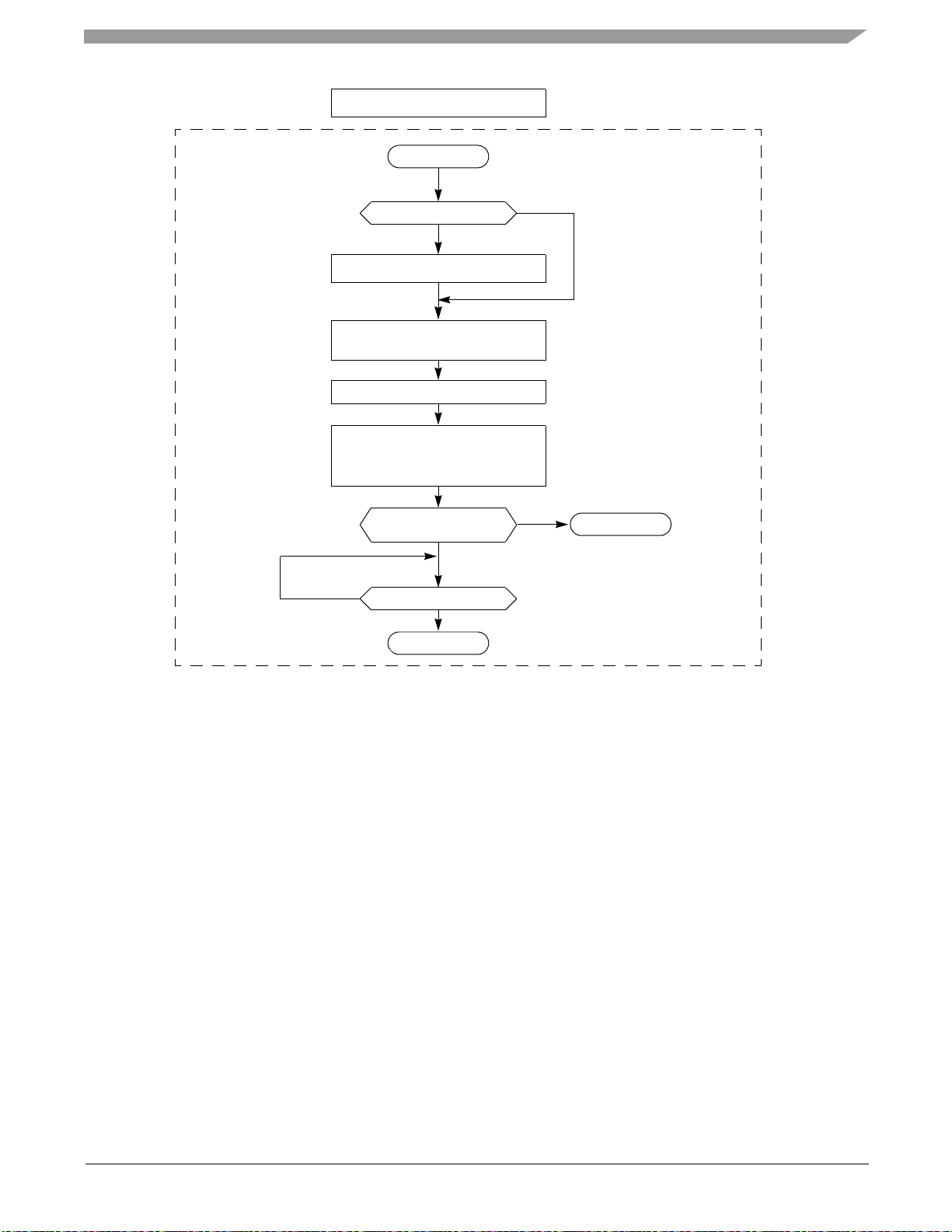
START
WRITE TO FLASH
TO BUFFER ADDRESS AND DATA
WRITE COMMAND TO FCMD
NO
YES
FPVIOL OR
WRITE 1 TO FCBEF
TO LAUNCH COMMAND
AND CLEAR FCBEF
(2)
1
0
FCCF?
ERROR EXIT
DONE
Note 2: Wait at least four bus cycles
0
FACCERR?
CLEAR ERROR
FACCERR?
WRITE TO FCDIV
(1)
Note 1: Required only once after reset.
1
before checking FCBEF or FCCF.
FLASH PROGRAM AND
ERASE FLOW
Figure 9. FLASH Program and Erase Flowchart
Programming time for the FLASH through the BDM function is dependent on the specific external BDM interface tool and
software being used. Consult tool vendor for programming times.
Sensors
Freescale Semiconductor, Inc. 25
FXTH870x6
Page 30
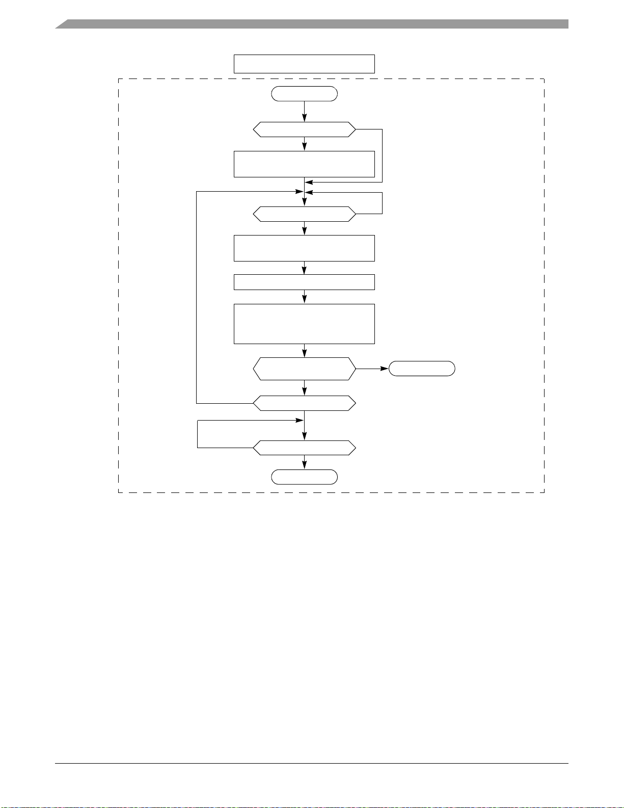
1
0
FCBEF?
START
WRITE TO FLASH
TO BUFFER ADDRESS AND DATA
WRITE COMMAND ($25) TO FCMD
NO
YES
FPVIO OR
WRITE 1 TO FCBEF
TO LAUNCH COMMAND
AND CLEAR FCBEF
(2)
NO
YES
NEW BURST COMMAND?
1
0
FCCF?
ERROR EXIT
DONE
Note 2: Wait at least four bus cycles before
1
0
FACCERR?
CLEAR ERROR
FACCERR?
Note 1: Required only once after reset.
WRITE TO FCDIV
(1)
checking FCBEF or FCCF.
FLASH BURST
PROGRAM FLOW
4.7.5 Access Errors
An access error occurs whenever the command execution protocol is violated.
Any of the following specific actions will cause the access error flag (FACCERR) in FSTAT to be set. FACCERR must be cleared
Figure 10. FLASH Burst Program Flowchart
by writing a 1 to FACCERR in FSTAT before any command can be processed.
• Writing to a FLASH address before the internal FLASH clock frequency has been set by writing to the FCDIV register
• Writing to a FLASH address while FCBEF is not set (A new command cannot be started until the command buffer is empty.)
• Writing a second time to a FLASH address before launching the previous command (There is only one write to FLASH for
every command.)
• Writing a second time to FCMD before launching the previous command (There is only one write to FCMD for every
command.)
• Writing to any FLASH control register other than FCMD after writing to a FLASH address
• Writing any command code other than the five allowed codes (0x05, 0x20, 0x25, 0x40, or 0x41) to FCMD
• Accessing (read or write) any FLASH control register other than the write to FSTAT (to clear FCBEF and launch the
command) after writing the command to FCMD.
• The MCU enters STOP mode while a program or erase command is in progress (The command is aborted.)
FXTH870x6
26 Freescale Semiconductor, Inc.
Sensors
Page 31

• Writing the byte program, burst program, or page erase command code (0x20, 0x25, or 0x40) with a BACKGROUND
FPS7 FPS6 FPS5 FPS4 FPS3 FPS2 FPS1
A15 A14 A13 A12 A11 A10 A9 A81A7 A6 A5 A4 A3 A2 A1 A0
11111111
DEBUG command while the MCU is secured (the BACKGROUND DEBUG controller can only do blank check and mass
erase commands when the MCU is secure.)
• Writing 0 to FCBEF to cancel a partial command.
4.7.6 FLASH Block Protection
The block protection feature prevents the protected region of FLASH from program or erase changes. Block protection is
controlled through the FLASH Protection Register (FPROT). When enabled, block prote c tion begins at any 512-byte boundary
below the last address of FLASH, 0xFFFF. (see Section 4.9.4).
After exit from reset, FPROT is loaded with the contents of the NVPROT location which is in the nonvolatile register block of the
FLASH memory. FPROT cannot be changed directly from application software so a runaway program cannot alter the block
protection settings. Because NVPROT is within the last 512 bytes of FLASH, if any amount of memory is protected, NVPROT is
itself protected and cannot be altered (intentionally or unintentionally) by the application software. FPROT can be written through
BACKGROUND DEBUG commands which allows a way to erase and reprogram a protected FLASH memory.
The block protection mechanism is illustrated below. The FPS bits are used as the upper bits of the last address of unprotected
memory. This address is formed by concatenating FPS7:FPS1 with logic 1 bits as shown. For example, in order to protect the
last 8192 bytes of memory (addresses 0xE000 through 0xFFFF), the FPS bits must be set to 1101 1 11 which results in the value
0xDFFF as the last address of unprotected memory. In addition to programming the FPS bits to the appropriate value, FPDIS (bit
0 of NVPROT) must be programmed to logic 0 to enable block protection. Therefore the value 0xDE must be programmed into
NVPROT to protect addresses 0xE000 through 0xFFFF.
Figure 11. Block Protection Mechanism
One use for block protection is to block protect an area of FLASH memo ry for a bootloader program. This bootloader program
then can be used to erase the rest of the FLASH memory and reprogram it. Because the bootloader is protected, it remains intact
even if MCU power is lost in the middle of an erase and reprogram operation.
4.7.7 Vector Redirection
NOTE
Not recommended for TPMS applications where Freescale firmware has been included in
the final image.
Whenever any block protection is enabled, the reset and interrupt vectors will be protected. Vector redirection allows users to
modify interrupt vector information without unprotecting bootloader and reset vector space. Vector redirection is enabled by
programming the FNORED bit in the NVOPT register located at address 0xFFBF to zero. For redirection to occur, at least some
portion but not all of the FLASH memory must be block protected by programming the NVPROT register located at address
0xFFBD. All of the interrupt vectors (memory locations 0xFFC0–0xFFFD) are redirected, though the reset vector (0xFFFE:FFFF)
is not.
For example, if 512 bytes of FLASH are protected, the protected address region is from 0xFE00 through 0xFFFF. The interrupt
vectors (0xFFC0–0xFFFD) are redirected to the locations 0xFDC0–0xFDFD. Now, if an SPI interrupt is taken for instance, the
values in the locations 0xFDE0:FDE1 are used for the vector instead of the values in the locations 0xFFE0:FFE1. This allows
the user to reprogram the unprotected portion of the FLASH with new program code including new interrupt vector values while
leaving the protected area, which includes the default vector locations, unchanged.
Sensors
Freescale Semiconductor, Inc. 27
FXTH870x6
Page 32

4.8 Security
The FXTH870x6 includes circuitry to prevent unauthorized access to the contents of FLASH and RAM memory. When security
is engaged, FLASH and RAM are considered secure resources. Direct-page registers, high-page registers, and the
BACKGROUND DEBUG controller are considered unsecured resources. Programs executing within secure memory have
normal access to any MCU memory locations and resources. Attempts to access a secure memory location with a program
executing from an unsecured memory space or through the BACKGROUND DEBUG interface are blocked (writes are ignored
and reads return all 0s).
Security is engaged or disengaged based on the state of two nonvolatile register bits (SEC0[1:0]) in the FOPT register. During
reset, the contents of the nonvolatile location NVOPT are copied from FLASH into the working FOPT register in high-page
register space. A user engages security by programming the NVOPT location, which can be done at the same time the FLASH
memory is programmed. The 1:0 state disengages security and the other three combinations engage security . Notice the erased
state (1:1) makes the MCU secure. During development, whenever the FLASH is erased, it is good practice to immediately
program the SEC00 bit to 0 in NVOPT so SEC[1:0] = 1:0. This would allow the MCU to remain unsecured after a subsequent
reset.
The on-chip debug module cannot be enabled while the MCU is secure. The separate BACKGROUND DEBUG controller can
still be used for background memory access commands, but the MCU cannot enter ACTIVE BACKGROUND mode except by
holding BKGD/MS low at the rising edge of reset.
A user can choose to allow or disallow a security unlocking mechanism through an 8-byte backdoor security key. If the nonvolatile
KEYEN bit in NVOPT/FOPT is 0, the backdoor key is disabled and there is no way to disengage security without completely
erasing all FLASH locations. If KEYEN is 1, a secure user program can temporarily disengage security by:
1. Writing 1 to KEYACC in the FCNFG register. This makes the FLASH module interpret writes to the backdoor
comparison key locations (NVBACKKEY through NVBACKKEY+7) as values to be compared against the key rather
than as the first step in a FLASH program or erase command.
2. Writing the user-entered key values to the NVBACKKEY through NVBACKKEY+7 locations. These writes must be
done in order starting with the value for NVBACKKEY and ending with NVBACKKEY+7. STHX must not be used for
these writes because these writes cannot be done on adjacent bus cycles. User software normally would get the key
codes from outside the MCU system through a communication interface such as a serial I/O.
3. Writing 0 to KEYACC in the FCNFG register. If the 8-byte key that was just written matches the key stored in the
FLASH locations, SEC[1:0] are automatically changed to 1:0 and security will be disengaged until the next reset.
The security key can be written only from secure memory (either RAM or FLASH), so it cannot be entered through
BACKGROUND commands without the cooperation of a secure user program.
The backdoor comparison key (NVBACKKEY through NVBACKKEY+7) is located in FLASH memory locations in the nonvolatile
register space so users can program these locations exactly as they would program any other FLASH memory location. The
nonvolatile registers are in the same 512-byte block of FLASH as the reset and interrupt vectors, so block protecting that space
also block protects the backdoor comparison key. Block protects cannot be changed from user application programs, so if the
vector space is block protected, the backdoor security key mechanism cannot permanently change the block protect, security
settings, or the backdoor key.
Security can always be disengaged through the BACKGROUND DEBUG interface by taking these steps:
1. Disable any block protections by writing FPROT . FPROT can be written only with BACKGROUND DEBUG commands,
not from application software.
2. Mass erase FLASH if necessary.
3. Blank check FLASH. Provided FLASH is completely erased, security is disengaged until the next reset.
To avoid returning to secure mode after the next reset, program NVOPT so SEC[1:0] = 1:0.
NOTE
Enabling the security feature disables Freescale ability to perform failure analysis without
first completely erasing all flash memory contents. If the security feature is implemented,
customer shall be responsible for providing to Freescale unsecured parts for any failure
analysis to begin or supplying the entire contents of the device flash memory data as part of
the return process, to allow Freescale to erase and subsequently restore the device to its
original condition.
FXTH870x6
Sensors
28 Freescale Semiconductor, Inc.
Page 33

4.9 FLASH Registers and Control Bits
The FLASH module has nine 8-bit registers in the high-page register space, three locations in the nonvolatile register space in
FLASH memory which are copied into three corresponding high-page control registers at reset. There is also an 8-byte
comparison key in FLASH memory. Refer to Table 8 and Table 9 for the absolute address assignments for all FLASH registers.
This section refers to registers and control bits only by their names. A Freescale Semiconductor-provided equate or header file
normally is used to translate these names into the appropriate absolute addresses.
4.9.1 FLASH Clock Divider Register (FCDIV)
Bit 7 of this register is a read-only status flag. Bits 6 through 0 can be read at any time but can be written only once. Before any
erase or programming operations are possible, write to this register to set the frequency of the clock for the nonvolatile memory
system within acceptable limits.
$1820 7 6 5 4 3 2 1 0
DIVLD
R
W
Reset:
00000000
Table 10. FCDIV Register Field Descriptions
Field Description
Divisor Loaded Status Flag — When set, this read-only status flag indicates that the FCDIV register has been written since
7
DIVLD
6
PRDIV8
5:0
DIV[5:0]
reset. Reset clears this bit and the first write to this register causes this bit to become set regardless of the data written.
0 FCDIV has not been written since reset; erase and program operations disabled for FLASH
1 FCDIV has been written since reset; erase and program operations enabled for FLASH
Prescale (Divide) FLASH Clock by 8
0 Clock input to the FLASH clock divider is the bus rate clock
1 Clock input to the FLASH clock divider is the bus rate clock divided by 8
Divisor for FLASH Clock Divider — The FLASH clock divider divides the bus rate clock (or the bus rate clock divided by 8 if
PRDIV8 = 1) by the value in the 6-bit DIV5:DIV0 field plus one. The resulting frequency of the internal FLASH clock must fall
within the range of 200 kHz to 150 kHz for proper FLASH operations. Program/Erase timing pulses are one cycle of this internal
FLASH clock which corresponds to a range of 5 s to 6.7 s. The automated programming logic uses an integer number of
these pulses to complete an erase or program operation.
• if PRDIV8 = 0 — f
• if PRDIV8 = 1 — f
Table 11 shows the appropriate values for PRDIV8 and DIV5:DIV0 for selected bus frequencies.
PRDIV8 DIV5 DIV4 DIV3 DIV2 DIV1 DIV0
= Reserved
Figure 12. FLASH Clock Di vider Register (FCDIV)
= f
FCLK
FCLK
([DIV5:DIV0] + 1)
Bus
= f
(8 ([DIV5:DIV0] + 1))
Bus
Table 11. FLASH Clock Divider Settings
f
Bus
20 MHz 1 12 192.3 kHz 5.2 s
10 MHz 0 49 200 kHz 5 s
8 MHz 0 39 200 kHz 5 s
4 MHz 0 19 200 kHz 5 s
2 MHz 0 9 200 kHz 5 s
1 MHz 0 4 200 kHz 5 s
200 kHz 0 0 200 kHz 5 s
150 kHz 0 0 150 kHz 6.7 s
PRDIV8
(Binary)
DIV5:DIV0
(Decimal)
f
FCLK
Program/Erase Timing Pulse
(5 s Min, 6.7s Max)
FXTH870x6
Sensors
Freescale Semiconductor, Inc. 29
Page 34

4.9.2 FLASH Options Register (FOPT and NVOPT)
During reset, the contents of the nonvolatile location NVOPT are copied from FLASH into FOPT. Bits 5 through 2 are not used
and always read 0. This register may be read at any time, but writes have no meaning or effect. To change the value in this
register, erase and reprogram the NVOPT location in FLASH memory as usual and then issue a new MCU reset.
$1821 7 6 5 4 3 2 1 0
KEYEN FNORED 0 0 0 0 SEC01 SEC00
R
W
Reset:
= Reserved
Table 12. FOPT Register Field Descriptions
Field Description
Backdoor Key Mechanism Enable — When this bit is 0, the backdoor key mechanism cannot be used to disengage security .
The backdoor key mechanism is accessible only from user (secured) firmware. BDM commands cannot be used to write key
7
KEYEN
6
FNORED
1:0
SEC0[1:0]
comparison values that would unlock the backdoor key. For more detailed information about the backdoor key mechanism, refer
to Section 4.8.”
0 No backdoor key access allowed
1 If user firmware writes an 8-byte value that matches the nonvolatile backdoor key (NVBACKKEY through NVBACKKEY+7
in that order), security is temporarily disengaged until the next MCU reset
Vector Redirection Disable — When this bit is 1, then vector redirection is disabled.
0 Vector redirection enabled
1 Vector redirection disabled
Security State Code — This 2-bit field determines the security state of the MCU as shown in Table 13. When the MCU is
secure, the contents of RAM and FLASH memory cannot be accessed by instructions from any unsecured source including the
BACKGROUND DEBUG interface. For more detailed information about security, refer to Section 4.8. SEC01:SEC00 changes
to 1:0 after successful backdoor key entry or a successful blank check of FLASH.
This register is loaded from nonvolatile location NVOPT during reset.
Figure 13. FLASH Options Register (FOPT)
Table 13. Security States
SEC01:SEC00 Description
0:0 secure
0:1 secure
1:0 unsecured
1:1 secure
4.9.3 FLASH Configuration Register (FCNFG)
Bits 7 through 5 can be read or written at any time. Bits 4 through 0 always read 0 and cannot be written.
$1823 7 6 5 4 3 2 1 0
Reset:
R
W
00
0 000 0 000
= Reserved
KEYACC
Figure 14. FLASH Configuration Register (FCNFG)
00000
FXTH870x6
Sensors
30 Freescale Semiconductor, Inc.
Page 35

Table 14. FCNFG Register Field Descriptions
Field Description
Enable Writing of Access Key — This bit enables writing of the backdoor comparison key. For more detailed information about
5
KEYACC
the backdoor key mechanism, refer to Section 4.8.
0 Writes to 0xFFB0–0xFFB7 are interpreted as the start of a FLASH programming or erase command
1 Writes to NVBACKKEY (0xFFB0–0xFFB7) are interpreted as comparison key writes
4.9.4 FLASH Protection Register (FPROT and NVPROT)
During reset, the contents of the nonvolatile location NVPROT is copied from FLASH into FPROT. Bits 0, 1, and 2 are not used
and each always reads as 0. This register can be read at any time, but user program writes have no meaning or effect.
BACKGROUND DEBUG commands can write to FPROT.
$1824 7 6 5 4 3 2 1 0
R
W
Reset:
1. Background commands can be used to change the contents of these bits in FPROT.
Table 15. FPROT Register Field Descripti ons
Field Description
7:1
FPS[7:1]
0
FPDIS
FPS7 FPS6 FPS5 FPS4 FPS3 FPS2 FPS1 FPDIS
(1)
(1) (1) (1) (1) (1) (1) (1)
This register is loaded from nonvolatile location NVPROT during reset.
Figure 15. FLASH Protection Register (FPROT)
FLASH Protect Select Bits — When FPDIS = 0, this 7-bit field determines the ending address of unprotected FLASH locations
at the high address end of the FLASH. Protected FLASH locations cannot be erased or programmed.
FLASH Protection Disable
0 FLASH block specified by FPS[7:1] is block protected (program and erase not allowed)
1 No FLASH block is protected
4.9.5 FLASH Status Register (FSTAT)
Bits 3, 1, and 0 always read 0 and writes have no meaning or effect. The remaining five bits are status bits that can be read at
any time. Writes to these bits have special meanings that are discussed in the bit descriptions.
$1825 7 6 5 4 3 2 1 0
FCCF
= Reserved
FPVIOL FACCERR
Reset:
R
FCBEF
W
11000000
Figure 16. FLASH Status Register (FSTAT)
Table 16. FSTAT Register Field Descriptions
Field Description
FLASH Command Buffer Empty Flag — The FCBEF bit is used to launch commands. It also indicates that the command
buffer is empty so that a new command sequence can be executed when performing burst programming. The FCBEF bit is
7
FCBEF
cleared by writing a one to it or when a burst program command is transferred to the array for programming. Only burst program
commands can be buffered.
0 Command buffer is full (not ready for additional commands)
1 A new burst program command can be written to the command buffer
0 FBLANK 0 0
FXTH870x6
Sensors
Freescale Semiconductor, Inc. 31
Page 36

Table 16. FSTAT Register Field Descriptions (continued)
Field Description
FLASH Command Complete Flag — FCCF is set automatically when the command buffer is empty and no command is being
6
FCCF
5
FPVIOL
4
FACCERR
2
FBLANK
processed. FCCF is cleared automatically when a new command is started (by writing 1 to FCBEF to register a command).
Writing to FCCF has no meaning or effect.
0 Command in progress
1 All commands complete
Protection Violation Flag — FPVIOL is set automatically when FCBEF is cleared to register a command that attempts to erase
or program a location in a protected block (the erroneous command is ignored). FPVIOL is cleared by writing a 1 to FPVIOL.
0 No protection violation
1 An attempt was made to erase or program a protected location
Access Error Flag — FACCERR is set automatically when the proper command sequence is not obeyed exactly (the
erroneous command is ignored), if a program or erase operation is attempted before the FCDIV register has been initialized ,
or if the MCU enters STOP while a command was in progress. For a more detailed discussion of the exact actions that are
considered access errors, see Section 4.7.5. FACCERR is cleared by writing a 1 to FACCERR. Writing a 0 to FACCERR has
no meaning or effect.
0 No access error
1 An access error has occurred
FLASH Verified as All Blank (erased) Flag — FBLANK is set automatically at the conclusion of a blank check command if
the entire FLASH array was verified to be erased. FBLANK is cleared by clearing FCBEF to write a new valid command. Writing
to FBLANK has no meaning or effect.
0 After a blank check command is completed and FCCF = 1, FBLANK = 0 indicates the FLASH array is not completely erased
1 After a blank check command is completed and FCCF = 1, FBLANK = 1 indicates the FLASH array is completely erased
(all 0xFF)
4.9.6 FLASH Command Register (FCMD)
Only five command codes are recognized in normal user modes as shown in Table 17. Refer to Section 4.7.3, for a detailed
discussion of FLASH programming and erase operations.
$1826 7 6 5 4 3 2 1 0
R
W
Reset:
00000000
FCMD7 FCMD6 FCMD5 FCMD4 FCMD3 FCMD2 FCMD1 FCMD0
00000000
Figure 17. FLASH Command Register (FCMD)
Table 17. FLASH Commands
Command FCMD Equate File Label
Blank check 0x05 mBlank
Byte program 0x20 mByteProg
Byte program — burst mode 0x25 mBurstProg
Page erase (512 bytes/page) 0x40 mPageErase
Mass erase (all FLASH) 0x41 mMassErase
All other command codes are illegal and generate an access error.
It is not necessary to perform a blank check command after a mass erase operation. Only blank check is required as part of the
security unlocking mechanism.
FXTH870x6
Sensors
32 Freescale Semiconductor, Inc.
Page 37

5 Reset, Interrupts and System Configuration
This section discusses basic reset and interrupt mechanisms and the various sources of reset and interrupts in the FXTH870x6.
Some interrupt sources from peripheral modules are discussed in greater detail within other sections of this product specification.
This section gathers basic information about all reset and interrupt sources in one place for easy reference. A few reset and
interrupt sources, including the computer operating properly (COP) watchdog and real-time interrupt (RTI), are not part of on-chip
peripheral systems, but are part of the system control logic.
5.1 Features
Reset and interrupt features include:
• Multiple sources of reset for flexible system configuration and reliable operation
• Reset status register (SRS) to indicate source of most recent reset
• Separate interrupt vectors for each module (reduces polling overhead)
5.2 MCU Reset
Resetting the MCU provides a way to start processing from a known set of initial conditions. During reset, most control and status
registers are forced to initial values and the program counter is loaded from the reset vector ($DFFE:$DFFF). On-chip peripheral
modules are disabled and any I/O pins are initially configured as general-purpose high-impedance inputs with any pullup devices
disabled. The I bit in the condition code register (CCR) is set to block maskable interrupts so the user program has a chance to
initialize the stack pointer (SP) and system control settings. The SP is forced to $00FF at reset. The FXTH870x6 has seven
sources for reset:
• Power-on reset (POR)
• Low-voltage detect (LVD)
• Computer operating properly (COP) timer
• Periodic hardware reset (PRST)
• Illegal opcode detect
• Illegal address detect
• BACKGROUND DEBUG forced reset
Each of these sources has an associated bit in the system reset status register with the exception of the BACKGROUND DEBUG
forced reset and the periodic hardware reset, PRST, that is indicated by the PRF bit in the PWUCS1 register.
5.3 Computer Operating Properly (COP) Watchdog
The COP watchdog is intended to force a system reset when the application software fails to execute as expected. To prevent a
system reset from the COP timer (when it is enabled), application software must reset the COP timer periodically. If the
application program gets lost and fails to reset the COP before it times out, a system reset is generated to force the system back
to a known starting point. The COP watchdog is enabled by the COPE bit in SIMOPT1 register. The COP timer is reset by writing
any value to the address of SRS. This write does not affect the data in the read-only SRS. Instead, the act of writing to this
address is decoded and sends a reset signal to the COP timer.
The timeout period can be selected by the COPCLKS and the COPT[2:0] bits as shown in Table 18. The COPCLKS bit selects
either the LFO or the CPU bus clock as the clocking source and the COPT[2:0] bits select the clock count required for a timeout.
The tolerances of these timeout periods is dependent on the selected clock source (LFO or HFO).
Table 18. COP Watchdog Timeout Period
COPT
COPCLKS
0 000 LFO 2
0 001 LFO 2
0 010 LFO 2
0 011 LFO 2
0 100 LFO 2
0 101 LFO 2
210
Clock
Source
COP
Overflow
Count
5
6
7
8
9
10
COP Overflow Time
(ms, nominal)
32
64
128
256
512
1024
FXTH870x6
Sensors
Freescale Semiconductor, Inc. 33
Page 38

Table 18. COP Watchdog Timeout Period (continued)
COPCLKS
COPT
210
Clock
Source
0 110 LFO 2
0 111 LFO 2
COP
Overflow
Count
11
11
COP Overflow Time
(ms, nominal)
2048
2048
BUSCLKS[1:0]
1:1 (0.5 MHz) 1:0 (1 MHz) 0:1 (2 MHz) 0:0 (4MHz)
1 000Bus Clock 2
1 001Bus Clock 2
1 010Bus Clock 2
1 011Bus Clock 2
1 100Bus Clock 2
1 101Bus Clock 2
1 110Bus Clock 2
1 111Bus Clock 2
13
14
15
16
17
18
19
19
16.384 8.192 4.096 2.048
32.768 16.384 8.192 4.096
65.536 32.768 16.384 8.192
131.072 65.536 32.768 16.384
262.144 131.072 65.536 32.768
524.288 262.144 131.072 65.536
1048.576 524.288 262.144 131.072
1048.576 524.288 262.144 131.072
After any reset, the COP timer is enabled. This provides a reliable way to detect code that is not executing as intended. If the
COP watchdog is not used in an application, it can be disabled by clearing the COPE bit in the write-once SIMOPT1 register.
Even if the application will use the reset default settings in COPE, COPCLKS and COPT[2:0], the user should still write to writeonce SIMOPT1 during reset initialization to lock in the settings. That way, they cannot be changed accidentally if the application
program gets lost.
The write to SRS that services (clears) the COP timer should not be placed in an interrupt service routine (ISR) because the ISR
could continue to be executed periodically even if the main application program fails. When the MCU is in ACTIVE
BACKGROUND DEBUG mode, the COP timer is temporarily disabled.
5.4 SIM Test Register (SIMTST)
The output of the temperature monitor is available using the SIM Test register as shown in Figure 18.
$180F Bit 7 654321Bit 0
TRO
RESET:
R
W
00111001
TRH
= Reserved
Figure 18. SIM Test Register (SIMTST)
Table 19. SIMTST Register Field Descriptions
Field Description
7
reserved
6:4
TRH
3:1
reserved
0
TRO
Reserved Bit — These bits are reserved for factory trim and should not be altered by the user.
Temperature Restart High threshold — Binary coded from 0x00 to 0x07; recommend applications overwrite to 0x06 at each
wakeup cycle.
Reserved Bit — These bits are reserved for factory trim and should not be altered by the user.
Temperature Restart Outside
1 TR module is outside the T
temperature falls back within the T
0 TR module is within the T
temperature falls back to the T
temperature range and will restart the MCU if the TRE bit is set and
REARM
RESET
RESET
temperature range.
RESET
temperature range and the MCU cannot be armed to restart when
range. The TRE bit cannot be set.
FXTH870x6
Sensors
34 Freescale Semiconductor, Inc.
Page 39

5.5 Interrupts
Interrupts provide a way to save the current CPU status and registers, execute an interrupt service routine (ISR), and then restore
the CPU status so processing resumes where it left off before the interrupt. Other than the software interrupt (SWI), which is a
program instruction, interrupts are caused by hardware events. The debug module can also generate an SWI under certain
circumstances.
If an event occurs in an enabled interrupt source, an associated read-only status flag will become set. The CPU will not respond
until and unless the local interrupt enable is a logic 1 to enable the interrupt. The I bit in the CCR must be a logic 0 to allow
interrupts. The global interrupt mask (I bit) in the CCR is initially set after reset which masks (prevents) all maskable interrupt
sources. The user program initializes the stack pointer and performs other system setup before clearing the I bit to allow the CPU
to respond to interrupts. When the CPU receives a qualified interrupt request, it completes the current instruction before
responding to the interrupt. The interrupt sequence follows the same cycle-by-cycle sequence as the SWI instruction and consists
of:
• Saving the CPU registers on the stack
• Setting the I bit in the CCR to mask further interrupts
• Fetching the interrupt vector for the highest-priority interrupt that is currently pending
• Filling the instruction queue with the first three bytes of program information starting from the address fetched from the
interrupt vector locations
While the CPU is responding to the interrupt, the I bit is automatically set to avoid the possibility of another interrupt interrupting
the ISR itself (this is called nesting of interrupts). Normally, the I bit is restored to 0 when the CCR is restored from the value
stacked on entry to the ISR. In rare cases, the I bit may be cleared inside an ISR (after clearing the status flag that generated the
interrupt) so that other interrupts can be serviced without waiting for the first service routine to finish. This practice is not
recommended for anyone other than the most experienced programmers because it can lead to subtl e program errors tha t are
difficult to debug.
The interrupt service routine ends with a return-from-interrupt (RTI) instruction which restores the CCR, A, X, and PC registers
to their pre interrupt values by reading the previously saved info rmation off the stack.
When two or more interrupts are pending when the I bit is cleared, the highest priority source is serviced first.
For compatibility with the M68HC08, the H register is not automatically saved and restored. It is good programming practice to
push H onto the stack at the start of the interrupt service routine (ISR) and restore it just before the RTI that is used to return from
the ISR.
5.5.1 Interrupt Stack Frame
Figure 18 shows the contents and organization of a stack frame. Before the interrupt, the stack pointer (SP) points at the next
available byte location on the stack. The current values of CPU registers are stored on the stack starting with the low-order byte
of the program counter (PCL) and ending with the CCR. After stacking, the SP points at the next available location on the stack
which is the address that is one less than the address where the CCR was saved. The PC value that is stacked is the address
of the instruction in the main program that would have executed next if the interrupt had not occurred.
When an RTI instruction is executed, these values are recovered from the stack in reverse order. As part of the RTI sequence,
the CPU fills the instruction pipeline by reading three bytes of program information, starting from the PC address just recovered
from the stack.
The status flag causing the interrupt must be acknowledged (cleared) before returning from the ISR. Typically, the flag should be
cleared at the beginning of the ISR so that if another interrupt is generated by this same source, it will be registered so it can be
serviced after completion of the current ISR.
FXTH870x6
Sensors
Freescale Semiconductor, Inc. 35
Page 40

Figure 19. Interrupt Stack Frame
CONDITION CODE REGISTER
ACCUMULATOR
INDEX REGISTER* (LOW BYTE X)
PROGRAM COUNTER HIGH
PROGRAM COUNTER LOW
UNSTACKING
ORDER
STACKING
ORDER
SP before
the interrupt
SP after
interrupt stacking
Towards HIGHER Addresses
Towards LOWER Addresses
70
1
2
3
4
5
5
4
3
2
1
* High byte (H) of index register is not automatically stacked.
5.5.2 Vect or Summary
Table 20 provides a summary of all interrupt sources. Higher-priority sources are located toward the bottom of the table (at the
higher vector addresses). All of these vectors are a 2-byte address that the firmware uses as the destination address. This allows
the firmware to intercept all vectors and add additional processing as needed. The additional process latency for each interrupt
will be described in Section 14.
Therefore, the high-order byte of the address for the user’s interrupt service routine is located at the lower address in the vector
address column, and the low-order byte of the address for the interrupt service routine is located at the higher address. When an
interrupt condition occurs, an asso ciated flag bit becom es set. If the associated local interrupt enable is set, an interrupt request
is sent to the CPU. Within the CPU, if the global interrupt mask (I bit in the CCR) is 0, the CPU will finish the current instruction,
stack the PCL, PCH, X, A, and CCR CPU registers, set the I bit, and then fetch the interrupt vector for the highest priority pending
interrupt. Processing then continues in the interrupt service routine.
The triggering of any of these vector fetches will wake the MCU from any of the STOP modes.
FXTH870x6
36 Freescale Semiconductor, Inc.
Sensors
Page 41

Table 20. Vector Summary
Vector
Priority
Lower
Higher
Vector
No.
15 $DFE0 - $DFE1 Vkbi KBI KBF KBIE Keyboard interrupt pins PTA[3:0]
14 $DFE2 - $DFE3
13 $DFE4 - $DFE5
12 $DFE6 - $DFE7 Vrti Sys Ctrl RTIF RTIE
11 $DFE8 - $DFE9 Vlfrcvr LFR
10 $DFEA - $DFEB
9 $DFEC - $DFED Vrf RFM
8$DFEE - $DFEF
7 $DFF0 - $DFF1 Vtpm1ovf TPM1 TOF TOIE
6 $DFF2 - $DFF3 Vtpm1ch1 TPM1 CH1F CH1IE
5 $DFF4 - $DFF5 Vtpm1ch0 TPM1 CH0F CH0IE
4 $DFF6 - $DFF7 Vwuktmr PWU WUKI WUK[5:0]
3 $DFF8 - $DFF9 Vlvd Sys Ctrl LVDF LVDIE
2$DFFA - $DFFB
1 $DFFC - $DFFD Vswi SWI opcode — —
0 $DFFE -$DFFF Vreset
Jump Table
Vector Addr
(High/Low)
Vector
Name
Module
Source
Sys Ctrl - POR — — Reset from power on sequence.
Sys Ctrl - PRF PRF PRST[5:0]
Sys Ctrl - COP — COPE Reset when COP watchdog times out.
Sys Ctrl - LVD — LVDRE
Temp Restart — TRE
Illegal opcode — —
Illegal address — —
Flags Enables Description
Reserved
Reserved
Interrupt from the RTI when the periodic
wakeup timer has timed out.
LFIDF LFIDIE
LFCDF LFCDIE
LFERF LFERIE
LFDRF LFDRIE
Reserved
RFIF
RFIEN
RFEF
Reserved
Reserved
Interrupt from LFR in data mode when a valid
wake ID has been received.
Interrupt from LFR in carrier mode when a
carrier present for the required time.
Interrupt from LFR in the manchester decode
mode when an error is detected.
Interrupt from LFR in the manchester decode
mode when an 8-bit data byte has been
successfully received.
Interrupt from the RFM when the data buffer
has been completely sent.
Interrupt from the RFM when transmission
error detected.
Interrupt from the TPM1 when the timer
overflows.
Interrupt from the TPM1 when the selected
event for channel 1 occurs.
Interrupt from the TPM1 when the selected
event for channel 0 occurs.
Interrupt from the PWU when the wakeup time
interval has elapsed.
Interrupt from the LVD when the supply
voltage has dropped below the LVD threshold.
Interrupt from the CPU when an SWI
instruction has been executed.
Reset from PWU when the reset interval
elapsed.
Reset from the LVD when the supply voltage
has dropped below the LVD threshold.
Reset when the temperature falls below the
temperature restart threshold
Reset from the CPU when trying to execute an
illegal opcode.
Reset from the CPU when trying to access an
illegal address.
FXTH870x6
Sensors
Freescale Semiconductor, Inc. 37
Page 42

5.6 Low-Voltage Detect (LVD) System
The FXTH870x6 includes a system to detect low voltage conditions in order to protect memory contents and control MCU system
states during supply voltage variations. The system is comprised of a power-on reset (POR) circuit and an LVD circuit with a user
selectable trip voltage, either high (V
voltage is selected by LVDV in SPMSC3. The LVD is disabled upon entering any of the STOP modes unless the LVDSE bit is
set. If LVDSE and LVDE are both set, then the MCU cannot enter STOP1.
5.6.1 Power-On Reset Operation
When power is initially applied to the FXTH870x6, or when the supply voltage drops below the V
cause a reset condition. As the supply voltage rises, the L VD circuit will hold the chip in reset until the supply has risen above the
level determined by LVDV bit. Both the POR bit and the LVD bit in SRS are set following a POR.
5.6.2 LVD Reset Operation
The LVD can be configured to generate a reset upon detection of a low voltage condition has occurred by setting LVDRE to 1
when the supply voltage has fallen below the level determined by LVDV bit. After an L VD reset has occurred, the LVD system will
hold the FXTH870x6 in reset until the supply voltage has risen above the level determined by L VDV bit. The threshold for falling
and rising differ by a small amount of hysteresis. The LVD bit in the SRS register is set following either an LVD reset or POR.
5.6.3 LVD Interrupt Operation
When a low voltage condition is detected and the LVD circuit is configured for interrupt operation (LVDE set, LVDIE set, and
LVDRE clear), then LVDF will be set and an LVD interrupt will occur.
5.6.4 Low-Voltage Warning (LVW)
The LVD system has a low voltage warning flag, LVWF, to indicate to the user that the supply voltage is approaching, but is still
above, the LVD reset voltage. The LVWF can be reset by writing a logical one to the LV WACK bit. The LVW does not have an
interrupt associated with it. There are two user selectable trip voltages for the LVW as selected by LVWV in SPMSC3. The L VWF
is set when the supply voltage falls below the selected level and cannot be reset until the supply voltage has ri sen above the
selected level. The threshold for falling and rising differ by a small amount of hysteresis.
LVDH
) or low (V
). The L VD circuit is enabled when L VDE in SPMSC1 is high and the trip
LVDL
level, the POR circuit will
POR
5.7 System Clock Control
Several clock rate selections are possible with the FXTH870x6 using the BUSCLKS[1:0] control bits to select the clock frequency
division of the HFO as given in Table 21. These bits are cleared by any MCU reset.
Table 21. HFO Frequency Selections
HFO Frequency
BUSCLKS1 BUSCLKS0
00 8 4
01 4 2
10 2 1
11 1 0.5
(MHz)
CPU Bus Frequency (MHz)
5.8 Keyboard Interrupts
The keyboard interrupts can be used to wake the MCU. These are assigned to specific general I/O pins as given in Table 22.
Table 22. Keyboard Interrupt Assignments
KBI Pin Pin Function
0 PTA0 General I/O
1 PTA1 General I/O
2 PTA2 General I/O
3 PTA3 General I/O
FXTH870x6
Sensors
38 Freescale Semiconductor, Inc.
Page 43

5.9 Real Time Interrupt
The RTI uses the internal low frequency oscillator (LFO) as its clock source. The RTI can be used as a periodic interrupt in MCU
RUN mode, or can be used as a periodic wakeup from all low power modes. The LFO is always active and cannot be powered
off by any software control. The control bits for the RTI are shown in Figure 20.
$1808 Bit 7 6 5 4 3 2 1 Bit 0
RTIF 0
RESET:
POR:
R
W
00000000
00000000
RTIACK
= Reserved
RTICLKS RTIE
Figure 20. RTI Status/Control Register (SRTISC)
Table 23. SRTISC Register Field Descripti ons
Field Description
RTI Interrupt Flag — The RTIF bit indicates when a wakeup interrupt has been generated by the RTI. This bit is cleared by
7
RTIF
6
RTIACK
5
RTICLKS
4
RTIE
3
Unused
2:0
RTIS[2:0]
writing a one to the RTIACK bit. Writing a zero to this bit has no effect. Reset clears this bit.
0 Wakeup interrupt not generated or was previously acknowledged.
1 Wakeup interrupt generated.
Acknowledge RTIF Interrupt Flag — The RTIACK bit clears the RTIF bit if written with a one. Writing a zero to the RTIACK bit
has no effect on the RTIF bit. Reading the RTIACK bit returns a zero. Reset has no effect on this bit.
0 No effect.
1 Clear RTIF bit.
RTI Interrupt Clock Select — This read-write bit selects the clock source for the real-time interrupt request
0 Real-time interrupt request clock source is the LFO.
1 Real-time interrupt request clock source is the HFO (MCU must be in the RUN mode).
RTIF Interrupt Enable — The RTIE bit enables RTI interrupts if written with a one. Reset clears this bit.
0 Disable RTI interrupts.
1 Enable RTI interrupts.
Unused
RTI Interrupt Delay Selects — The RTIS[2:0] bits select the timing of the RTI interrupts as given
in Table 24. Reset clears these bits.
0 RTIS[2:0]
FXTH870x6
Sensors
Freescale Semiconductor, Inc. 39
Page 44

Table 24. Real-Time Interrupt Period
RTIS2 RTIS1 RTIS0
000 OFF
001 2
010 4
011 8
100 16
101 32
110 64
111 128
Delay Timing (ms)
(Dependent on 1-kHz LFO)
5.10 Temperature Sensor and Restart System
The FXTH870x6 has two temperatur e sen si ng mechanisms. The first is an accurate sensor which is accessible through the
ADC10 channel 1. The second is a less accurate, very low power sensor which generates a wakeup from STOP1 when the
temperature crosses its threshold of detection. This is the temperature restart wakeup which is used as follows:
1. The temperature restart wakeup is enabled by software following detection of an over temperature condition using the
temperature sensor connected to the ADC10.
2. User software enables the temperature restart detector and then instructs the MCU to enter STOP1 mode to halt
execution during the out-of-range temperature condition.
3. When the temperature crosses the temperature restart threshold back into the normal range of operation, a wakeup is
generated to wake the MCU. Exit from STOP1 will reset the device.
The temperature sensor is enabled whenever the ADC10 is enabled. The temperature restart wakeup is enabled by setting the
TRE bit in SIMOPT1 register and whether the detector interrupts the MCU from a very low or a very high temperature is
determined by the TRH bit in the SIMOPT1 register.
5.11 Reset, Interrupt and System Control Registers And Bits
One 8-bit register in the direct page register space and eight 8-bit registers in the high-page register space are related to reset
and interrupt systems.
5.11.1 System Reset Status Register (SRS)
The SRS register at $1800 includes seven read-only status flags to indicate the source of the most recent reset. When a debug
host forces reset by writing 1 to BDFR in the SBDFR register, none of the status bits in SRS will be set. Writing any value to this
register address clears the COP watchdog timer without affecting the contents of this register. The reset state of these bits
depends on what caused the MCU to reset.
$1800 Bit 7 6 5 4 3 2 1 Bit 0
R
POR PIN COP ILOP ILAD PWU LVD
W
POR Reset:
LVD Reset:
Any Other
Reset:
1. Any of these reset sources that are active at the time of reset will cause the corresponding bit(s) to be set; bits corresponding to sources that
are not active at the time of reset will be cleared.
10000010
10000010
0
(1)(1)(1)(1)
= Reserved
000
Figure 21. System Reset Status Register (SRS)
0
FXTH870x6
Sensors
40 Freescale Semiconductor, Inc.
Page 45

Table 25. SRS Register Field Descriptions
Field Description
Power-On Reset — This bit indicates reset was caused by the power-on detection logic. Because the internal supply voltage
7
POR
6
PIN
5
COP
4
ILOP
3
ILAD
2
PWU
1
LVD
0
Unused
was ramping up at the time, the low-voltage reset (LVR) status bit is also set to indicate that the reset occurred while the internal
supply was below the LVR threshold.
0 Reset not caused by POR
1 POR caused reset
External Reset Pin — This bit indicates reset was caused by an active-low level on the external reset pin if the device was in
either the STOP1 or RUN modes. This bit is not set if the external reset pin is pulled low when the device is in the STOP1 mode.
0 Reset not caused by external reset pin
1 Reset came from external reset pin
Computer Operating Properly (COP) Watchdog — This bit indicates that reset was caused by the COP watchdog timer timing
out. This reset source may be blocked by COPE = 0.
0 Reset not caused by COP timeout
1 Reset caused by COP timeout
Illegal Opcode — This bit indicates reset was caused by an attempt to execute an unimplemented or illegal opcode. The STOP
instruction is considered illegal if STOP is disabled by STOPE = 0 in the SOPT register. The BGND instruction is considered
illegal if ACTIVE BACKGROUND mode is disabled by ENBDM = 0 in the BDCSC register.
0 Reset not caused by an illegal opcode
1 Reset caused by an illegal opcode
Illegal Address — This bit indicates reset was caused by an attempt to access either data or an instruction at an unimplemented
memory address.
0 Reset not caused by an illegal address
1 Reset caused by an illegal address
Programmable Wakeup — This bit indicates reset was caused by a PWU reset in run, WAIT , STOP4, and ST OP3. After STOP1
exit, PRF in PWUCSI indicates PWU was the source of a wakeup.
0 Reset not caused by PWU.
1 Reset caused by PWU.
Low Voltage Detect — If the L VDRE and LVDSE bits are set and the supply drops below the LVD trip voltage, an LVD reset will
occur. This bit is also set by POR.
0 Reset not caused by LVD trip or POR.
1 Reset caused by LVD trip or POR.
Unused Bit — This bit always reads as a logical zero. Writes
5.11.2 System Options Register 1 (SIMOPT1)
The following clock source and frequency selections are available using the system option register 1 as shown in Figure 22.
$1802 Bit 7 6 5 4 3 2 1 Bit 0
R
W
RESET:
Table 26. SIMOPT1 Register Field Descripti ons
Field Description
7
COPE
COPE COPCLKS STOPE RFEN TRE TRH BKGDPE
100-0011
= Reserved
Figure 22. System Option Register 1 (SIMOPT1)
COP Enable — This control bit enables the COP watchdog. This bit is a write-once bit so that only the first write after reset is
honored. Reset sets the COPE bit.
0 COP Watchdog disabled.
1 COP Watchdog enabled.
FXTH870x6
Sensors
Freescale Semiconductor, Inc. 41
Page 46

Table 26. SIMOPT1 Register Field Descriptions (continued)
Field Description
COP Clock Select — This control bit selects the clock source for the COP watchdog timer. This bit is a write-once bit so that
6
COPCLKS
5
STOPE
4
RFEN
3
TRE
2
TRH
1
BKGDPE
0
Reserved
only the first write after reset is honored. This bit is cleared by an MCU reset.
0 Select the LFO oscillator output.
1 Select the CPU bus clock.
STOP Mode Select — This control bit enables/disables the STOP instruction to enter a STOP mode defined by the SPMSCR2
register. This bit is a write-once bit so that only the first write after reset is honored. This bit is cleared by an MCU reset.
0 Disable STOP modes.
1 Enable STOP modes.
RF Module Enable — This bit enables or disables the RF module. This bit is not affected by any reset or power on after STOP
exit. It is only initialized at the first power up. This bit can be written anytime.
1 RF module enabled.
0 RF module disabled.
Temperature Restart Enable — This control bit enables the temperature restart circuit to interrupt the MCU after being
shutdown at either a very high or very low temperature. This bit is cleared by an MCU reset.
0 Temperature restart disabled.
1 Temperature restart enabled.
Temperature Restart Level — This control bit selects whether the temperature restart circuit will interrupt the MCU after being
shutdown on returning from either a very high or very low temperature. This bit is cleared by an MCU reset.
0 Temperature restart interrupts MCU on return from a very low temperature.
1 Temperature restart interrupts MCU on return from a very high temperature.
BKGD Pin Enable — BKGDPE can be used to allow the BKGD/PTA4 pin to be shared in applications as an input-only general
purpose I/O pin:
0 BKGD function disabled, PTA4 enabled.
1 BKGD function enabled, PTA4 disabled.
Reserved register bit, always reads 1.
5.11.3 System Operation Register 2 (SIMOPT2)
The following clock source and frequency selections are available using the system option register 2 as shown in Figure 23.
$1803 Bit 7 6 5 4 3 2 1 Bit 0
R
W
RESET:
Table 27. SIMOPT2 Register Field Descripti ons
Field Description
7
Unused
6:4
COPT[2:0]
3
LFOSEL
2
TCLKDIV
0 COPT[2:0] LFOSEL TCLKDIV BUSCLKS[1:0]
01110000
Figure 23. System Option Register 2 (SIMOPT2)
Unused Bit — This bit is unused and reads as a logic zero.
COP Watchdog Time Out — These control bits select the timeout period for the COP watchdog timer as given in Table 18.
These bits are set by an MCU reset to select the longest watchdog timeout period. These bits are write-once after power up.
TPM1 Channel 0 Clock Source — This bit determines which signal is connected to the TPM1 Channel 0, see Section 9.
0 Select clock input driven by PTA2.
1 Select clock input driven by the LFO.
TPM1 Channel 0 CLock Source Divider — The divider for the clock Source for TPM1 Channel 0, see Section 9.
0 Select RFM Dx clock source divided by 1.
1 Select RFM Dx clock source divided by 8.
FXTH870x6
Sensors
42 Freescale Semiconductor, Inc.
Page 47

Table 27. SIMOPT2 Register Field Descriptions (continued)
Field Description
Bus Clock Select — Bus clock frequency selection by changing HFO FLL ratio as shown in Figure 2. The bus clock frequency
1:0
BUSCLKS
[1:0]
is always the HFO frequency divided by two. These bits are cleared by a reset and can be written at any time.
00 Bus Frequency = 4 MHz (HFO = 8 MHz)
01 Bus Frequency = 2 MHz (HFO = 4 MHz)
10 Bus Frequency = 1 MHz (HFO = 2 MHz)
11 Bus Frequency = 0.5 MHz (HFO = 1 MHz)
5.11.4 System Power Management Status and Control 1 Register (SPMSC1)
$1809
R
W
Reset:
1. Bit 1 is a reserved bit that must always be written to 0.
2. This bit can be written only one time after reset. Additional writes are ignored.
765432
LVDF 0
LVDACK
00011100
= Reserved
LVDIE LVDRE
(2)
Figure 24. System Power Management Status and Control 1 Register (SPMSC1)
Table 28. SPMSC1 Register Field Descriptions
Field Description
7
LVDF
6
LVDACK
5
LVDIE
4
LVDRE
3
LVDSE
2
LVDE
0
Reserved
0
BGBE
Low-Voltage Detect Flag — Provided LVDE = 1, this read-only status bit indicates a low-voltage detect event.
Low-Voltage Detect Acknowledge — This write-only bit is used to acknowledge low voltage detection errors (write 1 to clear
LVDF). Reads always return logic 0.
Low-Voltage Detect Interrupt Enable — This read/write bit enables hardware interrupt requests for LVDF.
0 Hardware interrupt disabled (use polling)
1 Request a hardware interrupt when LVDF = 1
Low-Voltage Detect Reset Enable — This read/write bit enables LVDF events to generate a hardware reset (provided LVDE
= 1).
0 LVDF does not generate hardware resets
1 Force an MCU reset when LVDF = 1
Low-Voltage Detect Stop Enable — Provided LVDE = 1, this read/write bit determines whether the low-voltage detect function
operates when the MCU is in STOP mode.
0 Low-voltage detect disabled during STOP mode
1 Low-voltage detect enabled during STOP mode
Low-Voltage Detect Enable — This read/write bit enables low-voltage detect logic and qualifies the operation of other bits in
this register.
0 LVD logic disabled
1 LVD logic enabled
Reserved Bit — This bit is reserved should not be altered by the user. Any read returns a logical zero. Any write should be a
logical zero.
Bandgap Buffer Enable — The BGBE bit is used to enable an internal buf fer for the bandgap voltage reference for use by the
ADC module on one of its internal channels.
0 Bandgap buffer disabled
1 Bandgap buffer enabled
LVDSE LVDE
(1)
1
(2)
0BGBE
0
FXTH870x6
Sensors
Freescale Semiconductor, Inc. 43
Page 48

5.11.5 System Power Management Status and Control 2 Register (SPMSC2)
This register is used to configure the STOP mode behavior of the MCU.
$180A
R
W
Power-on reset:
Any other reset:
1. This bit can be written only one time after reset. Additional writes are ignored.
76543210
000PDF00
00000000
00UU0000
= Reserved U = Unaffected by reset
Figure 25. System Power Management Status and Control 2 Register (SPMSC2)
Table 29. SPMSC2 Register Field Descriptions
Field Description
7:5
Reserved
4
PDF
3
Reserved
2
PPDACK
1
PDC
0
Reserved
Reserved Bits — These bits are reserved should not be altered by the user. Any read returns a logical zero.
Power Down Flag — This read-only status bit indicates the MCU has recovered from STOP1 mode.
0 MCU has not recovered from STOP1 mode
1 MCU recovered from STOP1 mode
Reserved Bit — This bit is reserved should not be altered by the user. Any read returns a logical zero.
Partial Power Down Acknowledge — Writing a logic 1 to PPDACK clears the PDF bit.
Power Down Control — The PDC bit controls entry into the power down (STOP1) mode
0 Power down mode are disabled
1 Power down mode are enabled
Reserved Bit — This bit is reserved should not be altered by the user. Any read returns a logical zero. Any write should be a
logical zero.
PPDACK
PDC
(1)
0
5.11.6 System Power Management Status and Control 3 Register (SPMSC3)
$180C
R
W
Power-on reset:
LVD reset:
Any other reset:
1. LVWF will be set in the case when V
Table 30. SRTISC Register Field Descripti ons
Field Description
7
LVWF
Low-Voltage Warning Flag — The LVWF bit indicates the low voltage warning status.
0 Low voltage warning not present
1 Low voltage warning is present or was present
76543210
LVWF 0
LVWACK
(1)
0
(1)
0
(1)
0
= Reserved U = Unaffected by reset
Supply
LVDV LVWV
000 0 000
0UU 0 000
0UU 0 000
transitions below the trip point or after reset and V
0000
is already below V
Supply
Figure 26. System Power Management Status and Control 3 Register (SPMSC3)
LVW
.
FXTH870x6
Sensors
44 Freescale Semiconductor, Inc.
Page 49

Table 30. SRTISC Register Field Descriptions (continued)
Field Description
6
LVWACK
5
LVDV
4
LVWV
3:0
Reserved
Low-Voltage Warning Acknowledge — The LVWF bit indicates the low voltage warning status.
Writing a logic 1 to LVWACK clears LVWF to a logic 0 if a low voltage warning is not present.
Low-Voltage Detect Voltage Select — The LVDV bit selects the LVD trip point voltage (V
= V
= V
LVDL
LVDH
)
)
0 Low trip point selected (V
1 High trip point selected (V
LVD
LVD
Low-Voltage Warning Voltage Select — The LVWV bit selects the LVW trip point voltage (V
0 Low trip point selected (V
1 High trip point selected (V
LVW
LVW
= V
= V
LVDL
LVDH
)
)
LVD
).
LVW
).
Reserved Bits — These bits are reserved should not be altered by the user. Any read returns a logical zero.
5.12 System STOP Exit Status Register (SIMSES)
The SIMSES register at $180D can be used to determine the source of an MCU wakeup from the STOP modes. The flags are
as shown in Figure 27. All of the flags are automatically cleared when the MCU goes into a STOP mode. Writes to any of these
bits are ignored.
$180D Bit 7 6 5 4 3 2 1 Bit 0
R
W
RESET:
Reserved KBF IRQF TRF PWUF LFF RFF
00000000
= Reserved
Figure 27. SIM STOP Exit Status (SIMSES)
Table 31. SIMSES Register Field Descriptions
Field Description
7:6
Reserved
5
KBF
4
IRQF
3
TRF
2
PWUF
1
LFF
0
RFF
Reserved Bits — These bits are reserved for Freescale firmware control. Application software shall assure these two bits are
never overwritten.
Keyboard Flag — This bit indicates that any keyboard pin caused the last exit from STOP mode.
0 Keyboard pin did not cause the last exit from STOP mode
1 Keyboard pin caused the last exit from STOP mode
IRQ Flag — This bit indicates that IRQ pin caused the last exit from STOP mode.
0 IRQ pin did not cause the last exit from STOP mode
1 IRQ pin caused the last exit from STOP mode
Temperature Restart Flag — This bit indicates that the temperature restart module caused the last exit from STOP mode.
0 TR module did not cause the last exit from STOP mode
1 TR module caused the last exit from STOP mode
PWU Flag — This bit indicates that the PWU module caused the last exit from STOP mode.
0 PWU module did not cause the last exit from STOP mode
1 PWU module caused the last exit from STOP mode
LFR Flag — This bit indicates that the LFR module caused the last exit from STOP mode.
0 LFR module did not cause the last exit from STOP mode
1 LFR module caused the last exit from STOP mode
RFM Flag — This bit indicates that the RFM module caused the last exit from STOP mode.
0 RFM module did not cause the last exit from STOP mode
1 RFM module caused the last exit from STOP mode
FXTH870x6
Sensors
Freescale Semiconductor, Inc. 45
Page 50

6 General Purpose I/O
QD
QD
1
0
Port Read
PTxDDn
PTxDn
Output Enable
Output Data
Input Data
Synchronizer
Data
BUSCLKS
This section explains software controls related to general purpose input/output (I/O) and pin control. The FXTH870x6 has seven
general-purpose I/O pins which are comprised of a general use 5-bit port A and a 2-bit port B.
PTA[4:0] pins are shared with on-chip peripheral functions.
receiver, such that PTB[1:0] pins become high impedance when the LF is enabled (see Section 6.5 for additional details
regarding mutually exclusive operations). The peripheral modules have priority over the general purpose I/O so that when a
peripheral is enabled, the general purpose I/O functions associated with the shared pins are disabled. After reset, the shared
peripheral functions are disabled so that the pins are controlled by the general purpose I/O. All of the general purpose I/O are
configured as inputs (PTxDDn = 0) with pullup devices disabled (PTxPEn = 0).
T o avoid extra current drain from floating input pins, the user’s application software must configure these pins so that they do not
float (see Section 6.1).
Reading and writing of general purpose I/O is performed through the port data registers. The direction, either input or output, is
controlled through the port data direction registers. The general purpose I/O port function for an individual pin is illustrated in the
block diagram in Figure 28.
PTB[1:0] pins are GPIO only and are mutually exclusive with the LF
Figure 28. General Purpose I/O Block Diagram
FXTH870x6
46 Freescale Semiconductor, Inc.
Sensors
Page 51

Figure 29. General Purpose I/O Logic
PTxPEn
KBEDEy
KBIPGy
V
DD
PTxDn
RPU
RPD
PTxDDn
Write
PTxDn
Read
PTxPEn
KBEDGy
KBIPEy
KBI interrupt
KBACK
KBMOD
Port pin
PTA[3:0]
only
PTA[3:0]
only
Table 32. Truth Table for Pullup and Pulldown Resistors
PTAPE[3:0]
(pull enable)
0 0 x x disabled disabled
1 0 0 x enabled disabled
x 1 x x disabled disabled
1 0 1 0 enabled disabled
1 0 1 1 disabled enabled
PTBPE[1:0]
(pull enable)
0 0 x x disabled x
1 0 x x enabled x
x 1 x x disabled x
The data direction control bit (PTxDDn) determines whether the output buffer for the associated pin is enabled, and also controls
the source for port data register reads. The input buffer for the associated pin is always enabled unless the pin is enabled as an
analog function.
When a shared digital function is enabled for a pin, the output buffer is controlled by the shared function. However, the data
direction register bit still controls the source for reads of the port data register.
When a shared analog function is enabled for a pin, both the input and output buffers are disabled. A value of 0 is read for any
PTADD[3:0]
(data direction)
PTBDD[1:0]
(data direction)
KBIPE[3:0]
(KBI pin enable)
KBEDG[3:0]
(KBI Edge Select)
Pullup Pulldown
port data bit where the bit is an input (PTxDDn = 0) and the input buffer is disabled. In general, whenever a pin is shared with
both an alternate digital function and an analog function, the analog function has priority such that if both the digital and analog
functions are enabled, the analog function controls the pin.
It is a good programming practice to write to the port data register before changing the direction of a port pin to become an output.
This ensures that the pin will not be driven momentarily with an old data value that happened to be in the port data register.
FXTH870x6
Sensors
Freescale Semiconductor, Inc. 47
Page 52

An internal pullup device can be enabled for each port pin by setting the corresponding bit in one of the pullup enable registers
(PTxPEn). The pullup device is disabled if the pin is configured as an output by the general purpose I/O control logic or any shared
peripheral function regardless of the state of the corresponding pullup enable register bit. The pullup device is also disabled if the
pin is controlled by an analog function.
6.1 Unused Pin Configuration
Any general purpose I/O pins which are not used in the application must be properly configured to avoid a floating input that could
cause excessive supply current, I
When the device comes out of the reset state the Freescale supplied firmware will not configure any of the general purpose I/O
pins.
Recommended configuration methods are:
1. Configure the general purpose I/O pin as an input (PTxDDn = 0) with the pin connected to the VDD source; use a
pullup resistor of 10-51 k to assure sufficient noise immunity.
2. Configure the general purpose I/O pin as an input (PTxDDn = 0) with the internal pullup activated (PTxPEn = 1) and
leave the pin disconnected.
3. Configure the general purpose I/O pin as an output (PTxDDn = 1) and drive the pin low (PTxDn = 0) and leave the pin
disconnected.
In cases where GPIOs are directly connected to AV
an input with the internal pull-up disabled, in order to prevent software code faults from causing excessive supply current states
should these pins become outputs.
DD
.
, VDD, AVSS, VSS or RVSS, user application should configure the GPIO as
DD
6.2 Pin Behavior in STOP Modes
Pin behavior following execution of a STOP instruction depends on the STOP mode that is entered. An explanation of pin
behavior for the various STOP modes follows:
• In STOP1 mode, all internal registers including general purpose I/O control and data registers are powered off. Each of the
pins assumes its default reset state (input buffer, output buffer and internal pullup disabled). Upon exit from STOP1, all pins
must be reconfigured the same as if the MCU had been reset.
• In STOP4 mode, all pin states are maintained because internal logic stays powered up. Upon recovery, all pin functions are
the same as before entering STOP4.
6.3 General Purpose I/O Registers
This section provides information about the registers associated with the general purpose I/O ports and pin control functions.
These general purpose I/O registers are located in page zero of the memory map and the pin control registers are located in the
high page register section of memory.
6.4 Port A Registers
Port A general purpose I/O function is controlled by the registe rs de scribed in this section.
$0000 Bit 7 654321Bit 0
Reset:
R
W
00000000
= Reserved
Figure 30. Port A Data Register (PTAD)
PTAD[4:0]
FXTH870x6
Sensors
48 Freescale Semiconductor, Inc.
Page 53

Table 33. Port A Data Register Field Descriptions
Field Description
Port A Data Register Bit — For port A pins that are inputs, reads return the logic level on the pin. For port A pins that are
4:0
PTAD
[4:0]
$0001 Bit 7 654321Bit 0
configured as outputs, reads return the last value written to this register.
Writes are latched into all bits of this register. For port A pins that are configured as outputs, the logic level is driven out the
corresponding MCU pin.
Reset forces PTAD to all 0s, but these 0s are not driven out the corresponding pins because reset also configures all port pins
as high-impedance inputs with pullups disabled.
Reset:
R
W
00000000
= Reserved
PTAPE[3:0]
Figure 31. Internal Pullup Enable for Port A Register (PTAPE)
Table 34. Port A Register Pullup Enable Field Descriptions
Field Description
Internal Pullup Enable for Port A Bit n — Each of these control bits determines if the internal pullup device is enabled for the
3:0
PTAPE
[3:0]
associated PT A pin. For port A pins that are configured as outputs, these bits have no effect and the internal pullup devices are
disabled.
0 Internal pullup device disabled for port A bit n.
1 Internal pullup device enabled for port A bit n.
$0003 Bit 7 654321Bit 0
Reset:
R
W
00000000
= Reserved
PTADD[3:0]
Figure 32. Data Direction for Port A Register (PTADD)
Table 35. Port A Data Direction Field Descriptions
Field Description
3:0
PTADD
[3:0]
Data Direction for Port A Bit n — These read/write bits control the direction of port A pins and what is read for PTADD reads.
0 Input (output driver disabled) and reads return the pin value.
1 Output driver enabled for port A bit n and PTADD reads return the contents of PT A DDn. PTA4 is input-only, therefore bit 4 will
always be 0.
6.5 Port B Registers
Port B PTB[1:0] functions are multiplexed with the LF receiver block such that the port B GPIOs become high impedance when
the LF block has been enabled. When the LF block is disabled, port B pins operate as described here.
$0004 Bit 7 654321Bit 0
Reset:
R
W
00000000
= Reserved
PTBD[1:0]
Figure 33. Port B Data Register (PTBD)
FXTH870x6
Sensors
Freescale Semiconductor, Inc. 49
Page 54

Table 36. Port B Data Register Field Descriptions
Field Description
1:0
PTBD
[1:0]
$0005 Bit 7 654321Bit 0
Port B Data Register Bit n — For port B pins that are inputs, reads return the logic level on the pin. For port B pins that are
configured as outputs, reads return the last value written to this register.
Writes are latched into all bits of this register. For port B pins that are configured as outputs, the logic level is driven out the
corresponding MCU pin.
Reset forces PTBD to all 0s, but these 0s are not driven out the corresponding pins because reset also configures all port pins
as high-impedance inputs with pullups disabled.
Reset:
R
W
00000000
= Reserved
PTBPE[1:0]
Figure 34. Internal Pullup Enable for Port B Register (PTBPE)
Table 37. Port B Register Pullup Enable Field Descriptions
Field Description
Internal Pullup Enable for Port B Bit n — Each of these control bits determines if the internal pullup device is enabled for the
1:0
PTBPE
[1:0]
associated PTB pin. For port B pins that are configured as outputs, these bits have no effect and the internal pullup devices are
disabled.
0 Internal pullup device disabled for port B bit n.
1 Internal pullup device enabled for port B bit n.
$0007 B it 7 654321Bit 0
Reset:
R
W
00000000
= Reserved
PTBDD[1:0]
Figure 35. Data Direction for Port B Register (PTBDD)
Table 38. Port B Data Direction Field Descriptions
Field Description
1:0
PTBDD
[1:0]
Data Direction for Port B Bit n — These read/write bits control the direction of port B pins and what is read for PTBDD reads.
0 Input (output driver disabled) and reads return the pin value.
1 Output driver enabled for port B bit n and PTBDD reads return the contents of PTBDDn.
FXTH870x6
Sensors
50 Freescale Semiconductor, Inc.
Page 55

7 Keyboard Interrupt
DQ
CK
CLR
V
DD
KBMOD
KBIE
KEYBOARD
INTERRUPT FF
KBACK
RESET
SYNCHRONIZER
KBF
STOP BYPASS
STOP
BUSCLK
KBIPEn
0
1
S
KBEDGn
KBIPE0
0
1
S
KBEDG0
KBIP0
KBIPn
KBI
INTERRUP
The FXTH870x6 has a KBI module with general purpose I/O pins.
7.1 Features
The KBI features include:
• Up to four keyboard interrupt pins with individual pin enable bits.
• Each keyboard interrupt pin is programmable as falling edge (or rising edge) only, or both falling edge and low level (or both
rising edge and high level) interrupt sensitivity.
• One software enabled keyboard interrupt.
• Exit from low-power modes.
7.2 Modes of Operation
This section defines the KBI operation in WAIT, STOP, and BACKGROUND DEBUG modes.
7.2.1 KBI in STOP Modes
The KBI operates asynchronously in STOP4 mode if enabled before executing the STOP instruction. Therefore, an enabled KBI
pin (KBPE[3:0]) can be used to bring the MCU out of STOP4 mode if the KBI interrupt is enabled (KBIE = 1).
During STOP1 mode, the KBI is disabled. In some systems, the pins associated with the KBI may be sources of wakeup from
STOP1, see the STOP modes section in the Section 3. Upon wakeup from STOP1 mode, the KBI module will be in the reset
state.
7.2.2 KBI in ACTIVE BACKGROUND mode
When the microcontroller is in ACTIVE BACKGROUND mode, the KBI will continue to operate normally.
7.3 Block Diagram
The block diagram for the keyboard interrupt module is shown Figure 36.
Figure 36. KBI Block Diagram
7.4 External Signal Description
The KBI input pins can be used to detect either falling edges, or both falling edge and low level interrupt requests. The KBI input
pins can also be used to detect either rising edges, or both rising edge and high level interrupt requests. PTA[3:0] map to KBIPE
and KBEDG function bits [3:0].
The signal properties of KBI are shown in Table 39.
Sensors
Table 39. Signal Properties
Signal Function I/O
KBIPn Keyboard interrupt pins I
Freescale Semiconductor, Inc. 51
FXTH870x6
Page 56

7.5 Register Definitions
The KBI includes three registers:
• An 4-bit pin status and control register.
• An 4-bit pin enable register.
• An 4-bit edge select register.
7.5.1 KBI Status and Control Register (KBISC)
KBISC contains the status flag and control bits, which are used to configure the KBI.
$000C 7 6 5 4 3 2 1 0
R
W
Reset:
Table 40. KBISC Register Field Descriptions
Field Description
7:4 Unused register bits, always read 0.
3
KBF
2
KBACK
1
KBIE
0
KBMOD
0000KBF0
KBACK
00000000
= Reserved
KBIE KBMOD
Figure 37. KBI Status and Control Register
Keyboard Interrupt Flag — KBF indicates when a keyboard interrupt is detected. Writes have no effect on KBF.
0 No keyboard interrupt detected.
1 Keyboard interrupt detected.
Keyboard Acknowledge — Writing a 1 to KBACK is part of the flag clearing mechanism. KBACK always reads as 0.
Keyboard Interrupt Enable — KBIE determines whether a keyboard interrupt is requested.
0 Keyboard interrupt request not enabled.
1 Keyboard interrupt request enabled.
Keyboard Detection Mode — KBMOD (along with the KBEDG bits) controls the detection mode of the keyboard interrupt pins.
0 Keyboard detects edges only.
1 Keyboard detects both edges and levels.
7.5.2 KBI Pin Enable Register (KBIPE)
KBIPE contains the pin enable control bits.
$000D 7 6 5 4 3 2 1 0
R
W
Reset:
00000000
Figure 38. KBI Pin Enable Register
Table 41. KBIPE Register Field Descriptions
Field Description
3:0
KBIPEn
Keyboard Pin Enables — Each of the KBIPEn bits enable the corresponding keyboard interrupt pin.
0 Pin not enabled as keyboard interrupt.
1 Pin enabled as keyboard interrupt.
FXTH870x6
52 Freescale Semiconductor, Inc.
KBIPE3 KBIPE2 KBIPE1 KBIPE0
Sensors
Page 57

7.5.3 KBI Edge Select Register (KBIES)
KBIES contains the edge select control bits.
$000E 7 6 5 4 3 2 1 0
W
Reset:
R
00000000
KBEDG3 KBEDG2 KBEDG1 KBEDG0
Figure 39. KBI Edge Select Register
Table 42. KBIES Register Field Descriptions
Field Description
Keyboard Edge Selects — Each of the KBEDGn bits selects the falling edge/low level or rising edge/high level function of the
3:0
KBEDGn
corresponding pin).
0 Falling edge/low level.
1 Rising edge/high level.
7.6 Functional Description
This on-chip peripheral module is called a keyboard interrupt (KBI) module because originally it was designed to simplify the
connection and use of row-column matrices of keyboard switches. However, these inputs are also useful as extra external
interrupt inputs and as an external means of waking the MCU from STOP or WAIT low-power modes.
The KBI module allows up to eight pins to act as additional interrupt sources. Writing to the KBIPE[3:0] bits in the keyboard
interrupt pin enable register (KBIPE) independently enables or disables each KBI pin. Each KBI pin can be configured as edge
sensitive or edge and level sensitive based on the KBMOD bit in the keyboard interrupt status and control register (KBISC). Edge
sensitive can be software programmed to be either falling or rising; the level can be either low or high. The polarity of the edge
or edge and level sensitivity is selected using the KBEDG[3:0] bits in the keyboard interrupt edge select register (KBIES).
Synchronous logic is used to detect edges. Prior to detecting an edge, enabled keyboard inputs must be at the reset logic level.
A falling edge is detected when an enabled keyboard input signal is seen as a logic 1 (the reset level) during one bus cycle and
then a logic 0 (the asserted level) during the next cycle. A rising edge is detected when the input signal is seen as a logic 0 during
one bus cycle and then a logic 1 during the next cycle.
7.6.1 Edge Only Sensitivity
A valid edge on an enabled KBI pin will set KBF in KBISC. If KBIE in KBISC is set, an interrupt request will be presented to the
CPU. Clearing of KBF is accomplished by writing a 1 to KBACK in KBISC.
7.6.2 Edge and Level Sensitivity
A valid edge or level on an enabled KBI pin will set KBF in KBISC. If KBIE in KBISC is set, an interrupt request will be presented
to the CPU. Clearing of KBF is accomplished by writing a 1 to KBACK in KBISC provided all enabled keyboard inputs are at their
reset levels. KBF will remain set if any enabled KBI pin is asserted while attempting to clear by writing a 1 to KBACK.
7.6.3 KBI Pullup/Pulldown Resistors
The KBI pins can be configured to use an internal pullup/pulldown resistor using the associated I/O port pullup enable register.
If an internal resistor is enabled, the KBIES register is used to select whether the resistor is a pullup (KBEDG[3:0] = 0) or a
pulldown (KBEDG[3:0] = 1).
7.6.4 KBI Initialization
When a keyboard interrupt pin is first enabled it is possible to get a false keyboard interrupt flag. To prevent a false interrupt
request during keyboard initialization, the user should do the following:
1. Mask keyboard interrupts by clearing KBIE in KBISC.
2. Enable the KBI polarity by setting the appropriate KBEDGn bits in KBIES.
3. If using internal pullup/pulldown device, configure the associated pullup enable bits in PTAPE[3:0].
4. Enable the KBI pins by setting the appropriate KBIPE[3:0] bits in KBIPE.
5. Write to KBACK in KBISC to clear any false interrupts.
6. Set KBIE in KBISC to enable interrupts.
FXTH870x6
Sensors
Freescale Semiconductor, Inc. 53
Page 58

8 Central Processing Unit
8.1 Introduction
This section provides summary information about the registers, addressing modes, and instruction set of the CPU of the HCS08
Family. For a more det ailed discussion, refer to the HCS08 Family Reference Manual, volume 1, Freescale Semiconductor
document order number HCS08RMV1/D.
The HCS08 CPU is fully source- and object-code-compatible with the M68HC08 CPU. Several instructions and enhanced
addressing modes were added to improve C compiler efficiency and to support a new BACKGROUND DEBUG system which
replaces the monitor mode of earlier M68HC08 microcontrollers (MCU).
8.2 Features
Features of the HCS08 CPU include:
• Object code fully upward-compatible with M68HC05 and M68HC08 Families
• All registers and memory are mapped to a single 64-Kbyte address space
• 16-bit stack pointer (any size stack anywhere in 64-Kbyte address space)
• 16-bit index register (H:X) with powerful indexed addressing modes
• 8-bit accumulator (A)
• Many instructions treat X as a second general-purpose 8-bit register
• Seven addressing modes:
— Inherent — Operands in internal registers
— Relative — 8-bit signed offset to branch destination
— Immediate — Operand in next object code byte(s)
— Direct — Operand in memory at 0x0000–0x00FF
— Extended — Operand anywhere in 64-Kbyte address space
— Indexed relative to H:X — Five submodes including auto-increment
— Indexed relative to SP — Improves C efficiency dramatically
• Memory-to-memory data move instructions with four address mode combinations
• Overflow, half-carry, negative, zero, and carry condition codes support conditional branching on the results of signed,
unsigned, and binary-coded decimal (BCD) operations
• Efficient bit manipulation instructions
• Fast 8-bit by 8-bit multiply and 16-bit by 8-bit divide instructions
• STOP and WAIT instructions to invoke low-power operating modes
FXTH870x6
Sensors
54 Freescale Semiconductor, Inc.
Page 59

8.3 Programmer’s Model and CPU Registers
SP
PC
CONDITION CODE REGISTER
CARRY
ZERO
NEGATIVE
INTERRUPT MASK
HALF-CARRY (FROM BIT 3)
TWO’S COMPLEMENT OVERFLOW
H X
0
0
0
7
15
15
70
ACCUMULATOR
A
INDEX REGISTER (LOW)INDEX REGISTER (HIGH)
STACK POINTER
87
PROGRAM COUNTER
16-BIT INDEX REGISTER H:X
CCR
CV11HINZ
Figure 40 shows the five CPU registers. CPU registers are not part of the memory map.
Figure 40. CPU Registers
8.3.1 Accumulator (A)
The A accumulator is a general-purpose 8-bit register. One operand input to the arithmetic logic unit (ALU) is connected to the
accumulator and the ALU results are often stored into the A accumulator after arithmetic and logical operations. The accumulator
can be loaded from memory using various addressing modes to specify the address where the loaded data comes from, or the
contents of A can be stored to memory using various addressing modes to specify the address where data from A will be stored.
Reset has no effect on the contents of the A accumulator.
8.3.2 Index Register (H:X)
This 16-bit register is actually two separate 8-bit registers (H and X), which often work together as a 16-bit address pointer where
H holds the upper byte of an address and X holds the lower byte of the address. All indexed addressing mode instructions use
the full 16-bit value in H:X as an index reference pointer; however, for compatibility with the earlier M68HC05 Family, some
instructions operate only on the low-order 8-bit half (X).
Many instructions treat X as a second general-purpose 8-bit register that can be used to hold 8-bit data values. X can be cleared,
incremented, decremented, complemented, negated, shifted, or rotated. Transfer instructions allow data to be transferred from
A or transferred to A where arithmetic and logical operations can then be performed.
For compatibility with the earlier M68HC05 Family, H is forced to 0x00 during reset. Reset has no effect on the contents of X.
8.3.3 Stack Pointer (SP)
This 16-bit address pointer register points at the next available location on the automatic last-in-first-out (LIFO) stack. The stack
may be located anywhere in the 64-Kbyte address space that has RAM and can be any size up to the amount of available RAM.
The stack is used to automatically save the return address for subroutine calls, the return address and CPU registers during
interrupts, and for local variables. The AIS (add immediate to stack pointer) instruction adds an 8-bit signed immediate value to
SP. This is most often used to allocate or deallocate space for local variables on the stack.
SP is forced to 0x00FF at reset for compatibility with the earlier M68HC05 Family. HCS08 programs normally change the value
in SP to the address of the last location (highest address) in on-chip RAM during reset initialization to free up direct page RAM
(from the end of the on-chip registers to 0x00FF).
The RSP (reset stack pointer) instruction was included for compatibility with the M68HC05 Family and is seldom used in new
HCS08 programs because it only affects the low-order half of the stack pointer.
Sensors
Freescale Semiconductor, Inc. 55
FXTH870x6
Page 60

8.3.4 Program Counter (PC)
CONDITION CODE REGISTER
CARRY
ZERO
NEGATIVE
INTERRUPT MASK
HALF-CARRY (FROM BIT 3)
TWO’S COMPLEMENT OVERFLOW
70
CCR
CV11HINZ
The program counter is a 16-bit register that contains the address of the next instruction or operand to be fetched.
During normal program execution, the program counter automatically increments to the next sequential memory location every
time an instruction or operand is fetched. Jump, branch, interrupt, and return operations load the program counter with an
address other than that of the next sequential location. This is called a change-of-flow.
During reset, the program counter is loaded with the reset vector that is located at 0xFFFE and 0xFFFF. The vector stored there
is the address of the first instruction that will be executed after exiting the reset state.
8.3.5 Condition Code Register (CCR)
The 8-bit condition code register contains the interrupt mask (I) and five flags that indicate the results of the instruction just
executed. Bits 6 and 5 are set permanently to 1. The following paragraphs describe the functions of the condition code bits in
general terms. For a more detailed explanation of how each instruction sets the CCR bits, refer to the HCS08 Family Reference
Manual, volume 1, Freescale Semiconductor document order number HCS08RMv1.
Figure 41. Condition Code Register
Table 43. CCR Register Field Descriptions
Field Description
Two’s Complement Overflow Flag — The CPU sets the overflow flag when a two’s complement overflow occurs. The signed
branch instructions BGT, BGE, BLE, and BLT use the overflow flag.
7
V
H
N
0 No overflow
1Overflow
Half-Carry Flag — The CPU sets the half-carry flag when a carry occurs between accumulator bits 3 and 4 during an add-withoutcarry (ADD) or add-with-carry (ADC) operation. The half-carry flag is required for binary-coded decimal (BCD) arithmetic
operations. The DAA instruction uses the states of the H and C condition code bits to automatically add a correction value to the
4
result from a previous ADD or ADC on BCD operands to correct the result to a valid BCD value.
0 No carry between bits 3 and 4
1 Carry between bits 3 and 4
Interrupt Mask Bit — When the interrupt mask is set, all maskable CPU interrupts are disabled. CPU interrupts are enabled when
the interrupt mask is cleared. When a CPU interrupt occurs, the interrupt mask is set automatically after the CPU registers are
saved on the stack, but before the first instruction of the interrupt service routine is executed.
3
Interrupts are not recognized at the instruction boundary after any instruction that clears I (CLI or TAP). This ensures that the next
I
instruction after a CLI or TAP will always be executed without the possibility of an intervening interrupt, provided I was set.
0 Interrupts enabled
1 Interrupts disabled
Negative Flag — The CPU sets the negative flag when an arithmetic operation, logic operation, or data manipulation produces
a negative result, setting bit 7 of the result. Simply loading or storing an 8-bit or 16-bit value causes N to be set if the most
2
significant bit of the loaded or stored value was 1.
0 Non-negative result
1 Negative result
Zero Flag — The CPU sets the zero flag when an arithmetic operation, logic operation, or data manipulation produces a result
of 0x00 or 0x0000. Simply loading or storing an 8-bit or 16-bit value causes Z to be set if the loaded or stored value was all 0s.
1
0 Non-zero result
Z
1 Zero result
FXTH870x6
56 Freescale Semiconductor, Inc.
Sensors
Page 61

Table 43. CCR Register Field Descriptions (continued)
Field Description
Carry/Borrow Flag — The CPU sets the carry/borrow flag when an addition operation produces a carry out of bit 7 of the
accumulator or when a subtraction operation requires a borrow. Some instructions — such as bit test and branch, shift, and rotate
0
C
— also clear or set the carry/borrow flag.
0 No carry out of bit 7
1 Carry out of bit 7
8.4 Addressing Modes
Addressing modes define the way the CPU accesses operands and data. In the HCS08, all memory, status and control registers,
and input/output (I/O) ports share a single 64-Kbyte linear address space so a 16-bit b inary address can uniquely identify any
memory location. This arrangement means that the same instructions that access variables in RAM can also be used to ac cess
I/O and control registers or nonvolatile program space.
Some instructions use more than one addressing mode. For instance, move instructions use one addressing mode to specify the
source operand and a second addressing mode to specify the destination address. Instructions such as BRCLR, BRSET , CBEQ,
and DBNZ use one addressing mode to specify the location of an operand for a test and then use relative addressing mode to
specify the branch destination address when the tested condition is true. For BRCLR, BRSET , CBEQ, and DBNZ, the addressing
mode listed in the instruction set tables is the addressing mode needed to access the operand to be tested, and relative
addressing mode is implied for the branch destination.
8.4.1 Inherent Addressing Mode (INH)
In this addressing mode, operands needed to complete the instruction (if any) are located within CPU registers so the CPU does
not need to access memory to get any operands.
8.4.2 Relative Addressing Mode (REL)
Relative addressing mode is used to specify the destination location for branch instructions. A signed 8-bit offset value is located
in the memory location immediately following the opcode. During execution, if the branch condition is true, the signed offset is
sign-extended to a 16-bit value and is added to the current contents of the program counter, which causes program execution to
continue at the branch destination address.
8.4.3 Immediate Addressing Mode (IMM)
In immediate addressing mode, the operand needed to complete the instruction is included in the object code immediately
following the instruction opcode in memory. In the case of a 16-bit immediate operand, the high-order byte is located in the next
memory location after the opcode, and the low-order byte is located in the next memory location after that.
8.4.4 Direct Addressing Mode (DIR)
In direct addressing mode, the instruction includes the low-order eight bits of an address in the direct page (0x0000–0x00FF).
During execution a 16-bit address is formed by concatenating an implied 0x00 for the high-order half of the address and the direct
address from the instruction to get the 16-bit address where the desired operand is located. This is faster and more memory
efficient than specifying a complete 16-bit address for the operand.
8.4.5 Extended Addressing Mode (EXT)
In extended addressing mode, the full 16-bit address of the operand is located in the next two bytes of program memory after the
opcode (high byte first).
8.4.6 Indexed Addressing Mode
Indexed addressing mode has seven variations including five that use the 16-bit H:X index register pair and two that use the stack
pointer as the base reference.
8.4.6.1 Indexed, No Offset (IX)
This variation of indexed addressing uses the 16-bit value in the H:X index register pair as the address of the operand needed
to complete the instruction.
8.4.6.2 Indexed, No Offset with Post Increment (IX+)
This variation of indexed addressing uses the 16-bit value in the H:X index register pair as the address of the operand needed
to complete the instruction. The index register pair is then incremented (H:X = H:X + 0x0001) after the operand has been fetched.
This addressing mode is only used for MOV and CBEQ instructions.
FXTH870x6
Sensors
Freescale Semiconductor, Inc. 57
Page 62

8.4.6.3 Indexed, 8-Bit Offset (IX1)
This variation of indexed addressing uses the 16-bit value in the H:X index register pair plus an unsigned 8-bit offset included in
the instruction as the address of the operand needed to complete the instruction.
8.4.6.4 Indexed, 8-Bit Offset with Post Increment (IX1+)
This variation of indexed addressing uses the 16-bit value in the H:X index register pair plus an unsigned 8-bit offset included in
the instruction as the address of the operand needed to complete the instruction. The index register pair is then incremented
(H:X = H:X + 0x0001) after the operand has been fetched. This addressing mode is used only for the CBEQ instruction.
8.4.6.5 Indexed, 16-Bit Offset (IX2)
This variation of indexed addressing uses the 16-bit value in the H:X index register pair plus a 16-bit offset included in the
instruction as the address of the operand needed to complete the instruction.
8.4.6.6 SP-Relative, 8-Bit Offset (SP1)
This variation of indexed addressing uses the 16-bit value in the stack pointer (SP) plus an unsigned 8-bit offset included in the
instruction as the address of the operand needed to complete the instruction.
8.4.6.7 SP-Relative, 16-Bit Offset (SP2)
This variation of indexed addressing uses the 16-bit value in the stack pointer (SP) plus a 16-bit offset included in the instruction
as the address of the operand needed to complete the instruction.
8.5 Special Operations
The CPU performs a few special operations that are similar to instructions but do not have opcodes like other CPU instructions.
In addition, a few instructions such as STOP and WAIT directly affect other MCU circuitry. This section provides additional
information about these operations.
8.5.1 Reset Sequence
Reset can be caused by a power-on-reset (POR) event, internal conditions such as the COP (computer operating properly)
watchdog, or by assertion of an external active-low reset pin. When a reset event occurs, the CPU immediately stops whatever
it is doing (the MCU does not wait for an instruction boundary before responding to a reset event). For a more detailed discussion
about how the MCU recognizes resets and determines the source, refer to Section 5, “Reset, Interrupts and System
Configuration”.
The reset event is considered concluded when the sequence to determine whether the reset came from an internal source is
done and when the reset pin is no longer asserted. At the conclusion of a reset event, the CPU performs a 6-cycle sequence to
fetch the reset vector from 0xFFFE and 0xFFFF and to fill the instruction queue in preparation for execution of the first program
instruction.
8.5.2 Interrupt Sequence
When an interrupt is requested, the CPU completes the current instruction before responding to the interrupt. At this point, the
program counter is pointing at the start of the next instruction, which is where the CPU should return after servicing the interrupt.
The CPU responds to an interrupt by performing the same sequence of operations as for a software interrupt (SWI) instruction,
except the address used for the vector fetch is determined by the highest priority interrupt that is pending when the interrupt
sequence started.
The CPU sequence for an interrupt is:
1. Store the contents of PCL, PCH, X, A, and CCR on the stack, in that order.
2. Set the I bit in the CCR.
3. Fetch the high-order half of the interrupt vector.
4. Fetch the low-order half of the interrupt vector.
5. Delay for one free bus cycle.
6. Fetch three bytes of program information starting at the address indicated by the interrupt vector to fill the instruction
queue in preparation for execution of the first instruction in the interrupt service routine.
After the CCR contents are pushed onto the stack, the I bit in the CCR is set to prevent other interrupts while in the interrupt
service routine. Although it is possible to clear the I bit with an instruction in the interrupt service routine, this would allow nesting
of interrupts (which is not recommended because it leads to programs that are difficult to debug and maintain).
For compatibility with the earlier M68HC05 MCUs, the high-order half of the H:X index register pair (H) is not saved on the stack
as part of the interrupt sequence. The user must use a PSHH instruction at the beginning of the service routine to save H and
then use a PULH instruction just before the RTI that ends the interrupt service routine. It is not necessary to save H if you are
FXTH870x6
Sensors
58 Freescale Semiconductor, Inc.
Page 63

certain that the interrupt ser v ice routine does not use any instructions or auto-increment addressing modes that might change
the value of H.
The software interrupt (SWI) instruction is like a hardware interrupt except that it is not masked by the global I bit in the CCR and
it is associated with an instruction opcode within the program so it is not asynchronous to program execution.
8.5.3 WAIT Mode Operation
The WAIT instruction enables interrupts by clearing the I bit in the CCR. It then halts the clocks to the CPU to reduce overall
power consumption while the CPU is waiting for the interrupt or reset event that will wake the CPU from WAIT mode. When an
interrupt or reset event occurs, the CPU clocks will resume and the interrupt or reset event will be processed normally.
If a serial BACKGROUND command is issued to the MCU through the BACKGROUND DEBUG interface while the CPU is in
WAIT mode, CPU clocks will resume and the CPU will enter ACTIVE BACKGROUND mode where other serial BACKGROUND
commands can be processed. This ensures that a host development system can still gain access to a target MCU even if it is in
WAIT mode.
8.5.4 STOP Mode Operation
Usually, all system clocks, including the crystal oscillator (when used), are halted during STOP mode to minimize power
consumption. In such systems, external circuitry is needed to control the time spent in STOP mode and to issue a signal to
wakeup the target MCU when it is time to resume processing. Unlike the earlier M68HC05 and M68HC08 MCUs, the HCS08 can
be configured to keep a minimum set of clocks running in STOP mode. This optionally allows an internal periodic signal to wake
the target MCU from STOP mode.
When a host debug system is connected to the BACKGROUND DEBUG pin (BKGD) and the ENBDM control bit has been set
by a serial command through the BACKGROUND interface (or because the MCU was reset into ACTIVE BACKGROUND mode),
the oscillator is forced to remain active when the MCU enters STOP mode. In this case, if a serial BACKGROUND command is
issued to the MCU through the BACKGROUND DEBUG interface while the CPU is in STOP mode, CPU clocks will resume and
the CPU will enter ACTIVE BACKGROUND mode where other serial BACKGROUND commands can be processed. This
ensures that a host development system can still gain access to a target MCU even if it is in STOP mode.
Recovery from STOP mode depends on the particular HCS08 and whether the oscillator was stopped in STOP mode. Refer to
the Section 3 for more details.
8.5.5 BGND Instruction
The BGND instruction is new to the HCS08 compared to the M68HC08. BGND would not be used in normal user programs
because it forces the CPU to stop processing user instructions and enter the ACTIVE BACKGROUND mode. The only way to
resume execution of the user program is through reset or by a host debug system issuing a GO, TRACE1, or TAGGO serial
command through the BACKGROUND DEBUG interface.
Software-based breakpoints can be set by replacing an opcode at the desired breakpoint address with the BGND opcode. When
the program reaches this breakpoint address, the CPU is forced to ACTI VE BACKGROUND mode rather than continuing the
user program.
8.6 HCS08 Instruction Set Summary
Instruction Set Summary Nomenclature
The nomenclature listed here is used in the instruction descriptions in Table44.
Operators
( ) = Contents of register or memory location shown inside parentheses
= Is loaded with (read: “gets”)
& = Bool ean AND
| = Bool ean OR
= Boolean exclusive-OR
= Multiply
= Divide
: = Concatenate
+=Add
– = Negate (two’s complement)
CPU registers
A = Accumulator
CCR = Condition code register
H = Index register, higher order (most significant) 8 bits
FXTH870x6
Sensors
Freescale Semiconductor, Inc. 59
Page 64

X = Index register, lower order (least significant) 8 bits
PC = Program counter
PCH = Program counter, higher order (most significant) 8 bits
PCL = Program counter, lower order (least significant) 8 bits
SP = Stack pointer
Memory and addressing
M = A memory location or absol ute data, depending on addressing mode
M:M + 0x0001 = A 16-bit value in two consecutive memory locations. The higher-order (most significant) 8 bits are
located at the address of M, and the lower-order (least significant) 8 bits are located at the next higher
sequential address.
Condition code register (CCR) bits
V = Two’s complement overflow indicator, bit 7
H = Half carry, bit 4
I = Interrupt mask, bit 3
N = Negative indicator, bit 2
Z = Zero indicator, bit 1
C = Carry/borrow, bit 0 (carry out of bit 7)
CCR activity notation
– = Bit not affected
0 = Bit forced to 0
1 = Bit forced to 1
Þ = Bit set or cleared according to results of operation
U = Undefined after the operation
Machine coding notation
dd = Low-order 8 bits of a direct address 0x0000–0x00FF (high byte assumed to be 0x00)
ee = Upper 8 bits of 16-bit offset
ff = Lower 8 bits of 16-bit offset or 8-bit offset
ii = One byte of immediate data
jj = High-order byte of a 16-bit immediate data value
kk = Low-order byte of a 16-bit immediate data value
hh = High-order byte of 16-bit extended address
ll = Low-order byte of 16-bit extended address
rr = Relative offset
Source form
Everything in the source forms columns, except expressions in italic characters, is literal informa ti on that must appear in the
assembly source file exactly as shown. The initial 3- to 5-letter mnemonic is always a literal expression. All commas, pound signs
(#), parentheses, and plus signs (+) are literal characters.
n — Any label or expression that evaluates to a single integer in the range 0–7
opr8i — Any label or expression that evaluates to an 8-bit immediate value
opr16i — Any label or expression that evaluates to a 16-bit immediate value
opr8a — Any label or expression that evaluates to an 8-bit value. The instruction treats this 8-bit value as
the low order 8 bits of an address in the direct page of the 64-Kbyte address space (0x00xx).
opr16a — Any label or expression that evaluates to a 16-bit value. The instruction treats this value as an
address in the 64-Kbyte address space.
oprx8 — Any label or expression that evaluates to an unsigned 8-bit value, used for indexed addressing
oprx16 — Any label or expression that evaluates to a 16-bit value. Because the HCS08 has a 16-bit
address bus, this can be either a signed or an unsigned value.
rel — Any label or expression that refers to an address that is within –128 to +127 locations from the
next address after the last byte of object code for the current instruction. The assembler will
calculate the 8-bit signed offset and include it in the object code for this instruction.
FXTH870x6
Sensors
60 Freescale Semiconductor, Inc.
Page 65

Address modes
C
b0
b7
0
INH = Inherent (no operands)
IMM = 8-bit or 16-bit immediate
DIR = 8-bit direct
EXT = 16-bit extended
IX = 16-bit indexed no offset
IX+ = 16-bit indexed no offset, post increment (CBEQ and MOV only)
IX1 = 16-bit indexed with 8-bit offset from H:X
IX1+ = 16-bit indexed with 8-bit offset, post incr ement
(CBEQ only)
IX2 = 16-bit indexed with 16-bit offset from H:X
REL = 8-bit relative offset
SP1 = Stack pointer with 8-bit offset
SP2 = Stack pointer with 16-bit offset
Table 44. HCS08 Instruction Set Summary (Sheet 1 of 8)
Source
Form
ADC #opr8i
ADC opr8a
ADC opr16a
ADC oprx16,X
ADC oprx8,X
ADC ,X
ADC oprx16,SP
ADC oprx8,SP
ADD #opr8i
ADD opr8a
ADD opr16a
ADD oprx16,X
ADD oprx8,X
ADD ,X
ADD oprx16,SP
ADD oprx8,SP
AIS #opr8i
AIX #opr8i
AND #opr8i
AND opr8a
AND opr16a
AND oprx16,X
AND oprx8,X
AND ,X
AND oprx16,SP
AND oprx8,SP
ASL opr8a
ASLA
ASLX
ASL oprx8,X
ASL ,X
ASL oprx8,SP
Effect
on CCR
Operation Description
VHINZC
Add with Carry A (A) + (M) + (C) ÞÞ– ÞÞÞ
Add without Carry A (A) + (M) ÞÞ– ÞÞÞ
Add Immediate Value
Signed) to Stack Pointer
(
Add Immediate Value
(Signed) to Index
Register (H:X)
Logical AND A (A) & (M) 0 – – ÞÞ–
Arithmetic Shift Left
(Same as LSL)
M is sign extended to a 16-bit value
M is sign extended to a 16-bit value
SP (SP) + (M)
H:X (H:X) + (M)
––––––IMM A7ii 2
––––––IMM AFii 2
Þ ––ÞÞÞ
IMM
DIR
EXT
IX2
IX1
IX
SP2
SP1
IMM
DIR
EXT
IX2
IX1
IX
SP2
SP1
IMM
DIR
EXT
IX2
IX1
IX
SP2
SP1
DIR
INH
INH
IX1
IX
SP1
Address
Mode
Opcode
A9
B9
C9
D9
E9
F9
9ED9
9EE9
AB
BB
CB
DB
EB
FB
9EDB
9EEB
A4
B4
C4
D4
E4
F4
9ED4
9EE4
38
48
58
68
78
9E68
ii
dd
hh ll
ee ff
ff
ee ff
ff
ii
dd
hh ll
ee ff
ff
ee ff
ff
ii
dd
hh ll
ee ff
ff
ee ff
ff
dd
ff
ff
(1)
Operand
Bus Cycles
2
3
4
4
3
3
5
4
2
3
4
4
3
3
5
4
2
3
4
4
3
3
5
4
5
1
1
5
4
6
FXTH870x6
Sensors
Freescale Semiconductor, Inc. 61
Page 66

Table 44. HCS08 Instruction Set Summary (Sheet 2 of 8)
b0
b7
C
Effect
Source
Form
ASR opr8a
ASRA
ASRX
ASR oprx8,X
ASR ,X
ASR oprx8,SP
BCC rel Branch if Carry Bit Clear Branch if (C) = 0 – – – – – – REL 24 rr 3
BCLR n,opr8a Clear Bit n in Memory Mn 0 ––––––
BCS rel
BEQ rel Branch if Equal Branch if (Z) = 1 – – – – – – REL 27 rr 3
BGE rel
BGND
BGT rel
BHCC rel
BHCS rel
BHI rel Branch if Higher Branch if (C) | (Z) = 0 – – – – – – REL 22 rr 3
BHS rel
BIH rel Branch if IRQ Pin High Branch if IRQ pin = 1 – – – – – – REL 2F rr 3
BIL rel Branch if IRQ Pin Low Branch if IRQ pin = 0 – – – – – – REL 2E rr 3
BIT #opr8i
BIT opr8a
BIT opr16a
BIT oprx16,X
BIT oprx8,X
BIT ,X
BIT oprx16,SP
BIT oprx8,SP
BLE rel
BLO rel
BLS rel Branch if Lower or Same Branch if (C) | (Z) = 1
BLT rel
BMC rel
Operation Description
Arithmetic Shift Right Þ ––ÞÞÞ
Branch if Carry Bit Set
(Same as BLO)
Branch if Greater Than or
Equal To
(Signed Operands)
Enter ACTIVE BACKGROUND if ENBDM = 1
Branch if Greater Than
(Signed Operands)
Branch if Half Carry Bit
Clear
Branch if Half Carry Bit
Set
Branch if Higher or Same
(Same as BCC)
Bit Test
Branch if Less Than
or Equal To
(Signed Operands)
Branch if Lower
(Same as BCS)
Branch if Less Than
(Signed Operands)
Branch if Interrupt Mask
Clear
Commands Until GO, TRACE1, or
Branch if (C) = 1 – – – – – – REL 25 rr 3
Branch if (N V ––––––REL 90rr 3
Waits For and Processes BDM
TAGGO
Branch if (Z)| (N V
Branch if (H) = 0 – – – – – – REL 28 rr 3
Branch if (H) = 1 – – – – – – REL 29 rr 3
Branch if (C) = 0 – – – – – – REL 24 rr 3
(A) & (M)
(CCR Updated but Operands
Not Changed)
Branch if (Z)| (N V 1
Branch if (C) = 1
Branch if (N V 1
Branch if (I) = 0
–––
on CCR
Mode
VHINZC
––––––INH 82 5+
–––REL 92rr 3
0––ÞÞ–
––––––
––––––
––––––
––––––
––––––
Address
DIR
INH
INH
IX1
IX
SP1
DIR (b0)
DIR (b1)
DIR (b2)
DIR (b3)
DIR (b4)
DIR (b5)
DIR (b6)
DIR (b7)
IMM
DIR
EXT
IX2
IX1
IX
SP2
SP1
REL 93 rr 3
REL 25 rr 3
REL 23 rr 3
REL 91 rr 3
REL 2C rr 3
Opcode
37
47
57
67
77
9E67
13
15
17
19
1B
1D
1F
A5
B5
C5
D5
E5
F5
9ED5
9EE5
Operand
dd
ff
ff
11
dd
dd
dd
dd
dd
dd
dd
dd
ii
dd
hh ll
ee ff
ff
ee ff
ff
(1)
Bus Cycles
5
1
1
5
4
6
5
5
5
5
5
5
5
5
2
3
4
4
3
3
5
4
FXTH870x6
Sensors
62 Freescale Semiconductor, Inc.
Page 67

Table 44. HCS08 Instruction Set Summary (Sheet 3 of 8)
Effect
Source
Form
BMI rel Branch if Minus Branch if (N) = 1
BMS rel
BNE rel Branch if Not Equal Branch if (Z) = 0
BPL rel Branch if Plus Branch if (N) = 0
BRA rel Branch Always No Test
BRCLR n,opr8a,rel
BRN rel Branch Never Uses 3 Bus Cycles – – – – – – REL 21 rr 3
BRSET n,opr8a,rel
BSET n,opr8a Set Bit n in Memory Mn 1 ––––––
l Branch to Subroutine
BSR re
CBEQ opr8a,rel
CBEQA #opr8i,rel
CBEQX #opr8i,rel
CBEQ oprx8,X+,rel
CBEQ ,X+,rel
CBEQ oprx8,SP,rel
CLC Clear Carry Bit C 0 –––––0INH 98 1
CLI Clear Interrupt Mask Bit I 0 ––0–––INH 9A 1
CLR opr8a
CLRA
CLRX
CLRH
CLR oprx8,X
CLR ,X
CLR oprx8,SP
Operation Description
Branch if Interrupt Mask
Set
Branch if Bit n in Memory
Clear
Branch if Bit n in Memory
Set
push (PCL); SP (SP) – 0x0001
push (PCH); SP (SP) – 0x0001
Compare and Branch if
Equal
Clear
Branch if (I) = 1
Branch if (Mn) = 0 – – – – – Þ
Branch if (Mn) = 1 – – – – – Þ
PC (PC) + 0x0002
PC (PC) + rel
Branch if (A) = (M)
Branch if (A) = (M)
Branch if (X) = (M)
Branch if (A) = (M)
Branch if (A) = (M)
Branch if (A) = (M)
M 0x00
A 0x00
X
0x00
H 0x00
M 0x00
M 0x00
M 0x00
on CCR
Mode
VHINZC
––––––
––––––
––––––
––––––
––––––
––––––REL ADrr 5
––––––
0––
01–
Address
REL 2B rr 3
REL 2D rr 3
REL 26 rr 3
REL 2A rr 3
REL 20 rr 3
DIR (b0)
DIR (b1)
DIR (b2)
DIR (b3)
DIR (b4)
DIR (b5)
DIR (b6)
DIR (b7)
DIR (b0)
DIR (b1)
DIR (b2)
DIR (b3)
DIR (b4)
DIR (b5)
DIR (b6)
DIR (b7)
DIR (b0)
DIR (b1)
DIR (b2)
DIR (b3)
DIR (b4)
DIR (b5)
DIR (b6)
DIR (b7)
DIR
IMM
IMM
IX1+
IX+
SP1
DIR
INH
INH
INH
IX1
IX
SP1
Opcode
01
03
05
07
09
0B
0D
0F
00
02
04
06
08
0A
0C
0E
10
12
14
16
18
1A
1C
1E
31
41
51
61
71
9E61
3F
4F
5F
8C
6F
7F
9E6F
dd rr
dd rr
dd rr
dd rr
dd rr
dd rr
dd rr
dd rr
dd rr
dd rr
dd rr
dd rr
dd rr
dd rr
dd rr
dd rr
dd
dd
dd
dd
dd
dd
dd
dd
dd rr
ii rr
ii rr
ff rr
rr ff
rr
dd
ff
ff
(1)
Operand
5
5
5
5
5
5
5
5
5
5
5
5
5
5
5
5
5
5
5
5
5
5
5
5
5
4
4
5
5
6
5
1
1
1
5
4
6
Bus Cycles
FXTH870x6
Sensors
Freescale Semiconductor, Inc. 63
Page 68

Table 44. HCS08 Instruction Set Summary (Sheet 4 of 8)
Source
Form
CMP #opr8i
CMP opr8a
CMP opr16a
CMP oprx16,X
CMP oprx8,X
CMP ,X
CMP oprx16,SP
CMP oprx8,SP
COM opr8a
COMA
COMX
COM oprx8,X
COM ,X
COM oprx8,SP
CPHX opr16a
CPHX #opr16i
CPHX opr8a
CPHX oprx8,SP
CPX #opr8i
CPX opr8a
CPX opr16a
CPX oprx16,X
CPX oprx8,X
CPX ,X
CPX oprx16,SP
CPX oprx8,SP
DAA
DBNZ opr8a,rel
DBNZA rel
DBNZX rel
DBNZ oprx8,X,rel
DBNZ ,X,rel
DBNZ oprx8,SP,rel
DEC opr8a
DECA
DECX
DEC oprx8,X
DEC ,X
DEC oprx8,SP
DIV Divide
EOR #opr8i
EOR opr8a
EOR opr16a
EOR oprx16,X
EOR oprx8,X
EOR ,X
EOR oprx16,SP
EOR oprx8,SP
INC opr8a
INCA
INCX
INC oprx8,X
INC ,X
INC oprx8,SP
Compare Accumulator
with Memory
Complement
(One’s Complement)
Compare Index Register
(H:X) with Memory
Compare X (Index
Register Low) with
Memory
cimal Adjust
De
Accumulator After ADD
or ADC of BCD Values
Decrement and Branch if
Not Zero
Decrement
Exclusive OR
Memory with
Accumulator
Increment
Operation Description
(CCR Updated But Operands Not
(CCR Updated But Operands Not
(CCR Updated But Operands Not
(A) – (M)
Changed)
)= 0xFF – (M)
M (M
) = 0xFF – (A)
A (A
X (X
) = 0xFF – (X)
) = 0xFF – (M)
M (M
) = 0xFF – (M)
M (M
M (M
) = 0xFF – (M)
(H:X) – (M:M + 0x0001)
Changed)
(X) – (M)
Changed)
(A)
10
Decrement A, X, or M
Branch if (result) 0
DBNZX Affects X Not H
M (M) – 0x01
A (A) – 0x01
X (X) – 0x01
M (M) – 0x01
M (M) – 0x01
M (M) – 0x01
A (H:A)
H Remainder
A (A M) 0––ÞÞ–
M (M) + 0x01
A (A) + 0x01
X (X) + 0x01
M (M) + 0x01
M (M) + 0x01
M (M) + 0x01
(X)
Effect
on CCR
Mode
VHINZC
Þ ––ÞÞÞ
0––ÞÞ1
Þ ––ÞÞÞ
Þ ––ÞÞÞ
U––ÞÞÞINH 72 1
––––––
Þ ––ÞÞ–
–––
Þ ––ÞÞ–
–ÞÞINH 52 6
Address
IMM
DIR
EXT
IX2
IX1
IX
SP2
SP1
DIR
INH
INH
IX1
IX
SP1
EXT
IMM
DIR
SP1
IMM
DIR
EXT
IX2
IX1
IX
SP2
SP1
DIR
INH
INH
IX1
IX
SP1
DIR
INH
INH
IX1
IX
SP1
IMM
DIR
EXT
IX2
IX1
IX
SP2
SP1
DIR
INH
INH
IX1
IX
SP1
Opcode
A1
B1
C1
D1
E1
F1
9ED1
9EE1
33
43
53
63
73
9E63
3E
65
75
9EF3
A3
B3
C3
D3
E3
F3
9ED3
9EE3
3B
4B
5B
6B
7B
9E6B
3A
4A
5A
6A
7A
9E6A
A8
B8
C8
D8
E8
F8
9ED8
9EE8
3C
4C
5C
6C
7C
9E6C
Operand
ii
dd
hh ll
ee ff
ff
ee ff
ff
dd
ff
ff
hh ll
jj kk
dd
ff
ii
dd
hh ll
ee ff
ff
ee ff
ff
dd rr
rr
rr
ff rr
rr
ff rr
dd
ff
ff
ii
dd
hh ll
ee ff
ff
ee ff
ff
dd
ff
ff
(1)
Bus Cycles
2
3
4
4
3
3
5
4
5
1
1
5
4
6
6
3
5
6
2
3
4
4
3
3
5
4
7
4
4
7
6
8
5
1
1
5
4
6
2
3
4
4
3
3
5
4
5
1
1
5
4
6
FXTH870x6
Sensors
64 Freescale Semiconductor, Inc.
Page 69

Table 44. HCS08 Instruction Set Summary (Sheet 5 of 8)
C
b0
b7
0
b0
b7
C0
(1)
Operand
3
4
4
3
3
5
6
6
5
5
2
3
4
4
3
3
5
4
3
4
5
5
6
5
5
2
3
4
4
3
3
5
4
5
1
1
5
4
6
5
1
1
5
4
6
5
5
4
5
Source
Form
JMP opr8a
JMP opr16a
JMP oprx16,X
JMP oprx8,X
JMP ,X
JSR opr8a
JSR opr16a
JSR oprx16,X
JSR oprx8,X
JSR ,X
LDA #opr8i
LDA opr8a
LDA opr16a
LDA oprx16,X
LDA oprx8,X
LDA ,X
LDA oprx16,SP
LDA oprx8,SP
LDHX #opr16i
LDHX opr8a
LDHX opr16a
LDHX ,X
LDHX oprx16,X
LDHX oprx8,X
LDHX oprx8,SP
LDX #opr8i
LDX opr8a
LDX opr16a
LDX oprx16,X
LDX oprx8,X
LDX ,X
LDX oprx16,SP
LDX oprx8,SP
LSL opr8a
LSLA
LSLX
LSL oprx8,X
LSL ,X
LSL oprx8,SP
LSR opr8a
LSRA
LSRX
LSR oprx8,X
LSR ,X
LSR oprx8,SP
MOV opr8a,opr8a
MOV opr8a,X+
MOV #
opr8i,opr
MOV ,X+,opr8a
Effect
on CCR
Operation Description
VHINZC
Jump PC Jump Address – – – – – –
PC (PC) + n (n = 1, 2, or 3)
Jump to Subroutine
Push (PCL); SP (SP) – 0x0001
Push (PCH); SP (SP) – 0x0001
––––––
PC Unconditional Address
Load Accumulator from
Memory
Load Index Register
(H:X) from Memory
Load X (Index Register
Low) from Memory
Logical Shift Left
(Same as ASL)
A (M) 0––
H:X M:M+ 0x0001 0––ÞÞ–
X
(M) 0––ÞÞ–
Þ ––ÞÞÞ
Logical Shift Right Þ ––0ÞÞ
8a
Move
(M)
destination
H:X (H:X) + 0x0001 in
(M)
source
0––ÞÞ–
IX+/DIR and DIR/IX+ Modes
ÞÞ–
Address
DIR
EXT
IX2
IX1
IX
DIR
EXT
IX2
IX1
IX
IMM
DIR
T
EX
IX2
IX1
IX
SP2
SP1
IMM
DIR
EXT
IX
IX2
IX1
SP1
IMM
DIR
T
EX
IX2
IX1
IX
SP2
SP1
DIR
INH
INH
IX1
IX
SP1
DIR
INH
INH
IX1
IX
SP1
DIR/DIR
DIR/IX+
IMM/DIR
IX+/DIR
Mode
Opcode
BC
CC
DC
EC
FC
BD
CD
DD
ED
FD
A6
B6
C6
D6
E6
F6
9ED6
9EE6
45
55
32
9EAE
9EBE
9ECE
9EFE
AE
BE
CE
DE
EE
FE
9EDE
9EEE
38
48
58
68
78
9E68
34
44
54
64
74
9E64
4E
5E
6E
7E
dd
hh ll
ee ff
ff
dd
hh ll
ee ff
ff
ii
dd
hh ll
ee ff
ff
ee ff
ff
jj kk
dd
hh ll
ee ff
ff
ff
ii
dd
hh ll
ee ff
ff
ee ff
ff
dd
ff
ff
dd
ff
ff
dd dd
dd
ii dd
dd
MUL Unsigned multiply X:A (X) (A) –0–––0INH 42 5
NEG opr8a
NEGA
NEGX
NEG oprx8,X
NEG ,X
NEG oprx8,SP
Negate
(Two’s Complement)
M – (M) = 0x00 – (M)
A – (A) = 0x00 – (A)
X – (X) = 0x00 – (X)
M – (M) = 0x00 – (M)
M – (M) = 0x00 – (M)
M – (M) = 0x00 – (M)
Þ ––ÞÞÞ
DIR
INH
INH
IX1
IX
SP1
30
40
50
60
70
9E60
dd
ff
ff
5
1
1
5
4
6
NOP No Operation Uses 1 Bus Cycle – – – – – – INH 9D 1
Bus Cycles
FXTH870x6
Sensors
Freescale Semiconductor, Inc. 65
Page 70

Table 44. HCS08 Instruction Set Summary (Sheet 6 of 8)
C
b0
b7
b0
b7
C
(1)
Operand
2
3
4
4
3
3
5
4
5
1
1
5
4
6
5
1
1
5
4
6
Source
Form
NSA
Operation Description
Nibble Swap
Accumulator
ORA #opr8i
ORA opr8a
ORA opr16a
ORA oprx16,X
ORA oprx8,X
Inclusive OR
Accumulator and Memory
ORA ,X
ORA oprx16,SP
ORA oprx8,SP
PSHA
PSHH
PSHX
PULA
PULH
PULX
Push Accumulator onto
Stack
Push H (Index Register
High) onto Stack
Push X (Index Register
Low) onto Stack
Pull Accumulator from
Stack
Pull H (Index Register
High) from Stack
Pull X (Index Register
Low) from Stack
ROL opr8a
ROLA
ROLX
ROL oprx8,X
Rotate Left through Carry Þ ––ÞÞÞ
ROL ,X
ROL oprx8,SP
ROR opr8a
RORA
RORX
ROR oprx8,X
Rotate Right through
Carry
ROR ,X
ROR oprx8,SP
RSP Reset Stack Pointer
Effect
on CCR
Mode
VHINZC
Address
Opcode
A (A[3:0]:A[7:4]) – – – – – – INH 62 1
A (A) | (M) 0 – – ÞÞ–
IMM
DIR
EXT
IX2
IX1
IX
SP2
SP1
AA
BA
CA
DA
EA
FA
9EDA
9EEA
ii
dd
hh ll
ee ff
ff
ee ff
ff
Push (A); SP (SP) – 0x0001 – – – – – – INH 87 2
Push (H); SP (SP) – 0x0001 – – – – – – INH 8B 2
Push (X); SP (SP) – 0x0001 – – – – – – INH 89 2
SP (SP + 0x0001); PullA ––––––INH 86 3
SP (SP + 0
x0001); PullH ––––––INH 8A 3
SP (SP + 0x0001); PullX ––––––INH 88 3
SP 0xFF
(High Byte Not Affected)
DIR
INH
INH
IX1
IX
SP1
DIR
INH
Þ ––ÞÞÞ
INH
IX1
IX
SP1
––––––INH 9C 1
39
49
59
69
79
9E69
36
46
56
66
76
9E66
dd
ff
ff
dd
ff
ff
SP (SP) + 0x0001; Pull (CCR)
SP (SP) + 0x0001; Pull (A)
RTI Return from Interrupt
SP
(SP) + 0x0001;
Pull (X)
ЮЮЮЮЮЮINH 80 9
SP (SP) + 0x0001; Pull (PCH)
SP (SP) + 0x0001; Pull (PCL)
RTS Return from Subroutine
SBC #opr8i
SBC opr8a
SBC opr16a
SBC oprx16,X
SBC oprx8,X
Subtract with Carry A (A) – (M) – (C) Þ ––ÞÞÞ
SBC ,X
SBC oprx16,SP
SBC oprx8,SP
SP SP + 0x0001PullPCH)
SP SP + 0x0001; Pull (PCL)
––––––INH 81 6
IMM
DIR
EXT
IX2
IX1
IX
SP2
SP1
A2
B2
C2
D2
E2
F2
9ED2
9EE2
ii
dd
hh ll
ee ff
ff
ee ff
ff
2
3
4
4
3
3
5
4
SEC Set Carry Bit C 1 –––––1INH 99 1
SEI Set Interrupt Mask Bit I 1 ––1–––INH 9B 1
Bus Cycles
FXTH870x6
66 Freescale Semiconductor, Inc.
Sensors
Page 71

Table 44. HCS08 Instruction Set Summary (Sheet 7 of 8)
Source
Form
STA opr8a
STA opr16a
STA oprx16,X
STA oprx8,X
STA ,X
STA oprx16,SP
STA oprx8,SP
STHX opr8a
STHX opr16a
STHX oprx8,SP
STOP
STX opr8a
STX opr16a
STX oprx16,X
STX oprx8,X
STX ,X
STX oprx16,SP
STX oprx8,SP
SUB #opr8i
SUB opr8a
SUB opr16a
SUB oprx16,X
SUB oprx8,X
SUB ,X
SUB oprx16,SP
SUB oprx8,SP
SWI Software Interrupt
P
TA
TAX
TPA
TST opr8a
TSTA
TSTX
TST oprx8,X
TST ,X
TST oprx8,SP
TSX
TXA
TXS
Operation Description
Store Accumulator in
Memory
Store H:X (Index Reg.) (M:M + 0x0001) (H:X) 0 – – ÞÞ–
Enable Interrupts:
Stop Processing
Refer to MCU Documentation
Store X (Low 8 Bits of
Index Register)
in Memory
Subtract A (A) – (M) Þ ––ÞÞÞ
Transfer Accumulator to
CCR
Transfer Accumulator to
X (Index Register Low)
Transfer CCR to Accumulator
Test for Negative or Zero
Transfer SP to Index
Reg.
Transfer X (Index Reg.
Low) to Accumulator
Transfer Index Reg. to
SP
Effect
on CCR
Mode
VHINZC
M (A) 0––ÞÞ–
I bit 0; Stop Processing – – 0 – – – INH 8E 2+
M (X) 0––ÞÞ
PC (PC) + 0x0001
Push (PCL); SP (SP) – 0x0001
Push (PCH); SP (SP) – 0x0001
Push (X); SP (SP) – 0x0001
Push (A); SP (SP) – 0x0001
Push (CCR); SP (SP) – 0x0001
I 1;
PCH Interrupt Vector High Byte
PCL Interrupt Vector Low Byte
CCR (A) ЮЮЮЮЮЮINH 84 1
X (A) ––––––INH 97 1
A (CCR) ––––––INH 85 1
(M) – 0x00
(A) – 0x00
(X) – 0x00
(M) – 0x00
(M) – 0x00
(M) – 0x00
H:X (SP) + 0x0001 – – – – – – INH 95 2
A (X) ––––––INH 9F 1
SP (H:X) – 0x0001 – – – – – – INH 94 2
––1–––INH 83 11
0––ÞÞ–
Address
DIR
EXT
IX2
IX1
IX
SP2
SP1
DIR
EXT
SP1
DIR
T
EX
IX2
IX1
–
IX
SP2
SP1
IMM
DIR
EXT
IX2
IX1
IX
SP2
SP1
DIR
INH
INH
IX1
IX
SP1
Opcode
B7
C7
D7
E7
F7
9ED7
9EE7
35
96
9EFF
BF
CF
DF
EF
FF
9EDF
9EEF
A0
B0
C0
D0
E0
F0
9ED0
9EE0
3D
4D
5D
6D
7D
9E6D
dd
hh ll
ee ff
ff
ee ff
ff
dd
hh ll
ff
dd
hh ll
ee ff
ff
ee ff
ff
ii
dd
hh ll
ee ff
ff
ee ff
ff
dd
ff
ff
(1)
Operand
Bus Cycles
3
4
4
3
2
5
4
4
5
5
3
4
4
3
2
5
4
2
3
4
4
3
3
5
4
4
1
1
4
3
5
FXTH870x6
Sensors
Freescale Semiconductor, Inc. 67
Page 72

Table 44. HCS08 Instruction Set Summary (Sheet 8 of 8)
Effect
on CCR
VHINZC
Address
Mode
WAIT
Source
Form
Operation Description
Enable Interrupts; Wait
for Interrupt
I bit 0; Halt CPU – – 0 – – – INH 8F 2+
1. Bus clock frequency is one-half of the CPU clock frequency.
Table 45. Opcode Map (Sheet 1 of 2)
Bit-Manipulation Branch Read-Modify-Write Control Register/Memory
00 5
BRSET0
3DIR
01 5
BRCLR0
3DIR
02 5
BRSET1
3DIR
03 5
BRCLR1
3DIR
04 5
BRSET2
3DIR
05 5
BRCLR2
3DIR
06 5
BRSET3
3DIR
07 5
BRCLR3
3DIR
08 5
BRSET4
3DIR
09 5
BRCLR4
3DIR
0A 5
BRSET5
3DIR
0B 5
BRCLR5
3DIR
0C 5
BRSET6
3DIR
0D 5
BRCLR6
3DIR
0E 5
BRSET7
3DIR
0F 5
BRCLR7
3DIR
10 5
BSET0
2DIR
11 5
BCLR0
2DIR
12 5
BSET1
2DIR
13 5
BCLR1
2DIR
14 5
BSET2
2DIR
15 5
BCLR2
2DIR
16 5
BSET3
2DIR
17 5
BCLR3
2DIR
18 5
BSET4
2DIR
19 5
BCLR4
2DIR
1A 5
BSET5
2DIR
1B 5
BCLR5
2DIR
1C 5
BSET6
2DIR
1D 5
BCLR6
2DIR
1E 5
BSET7
2DIR
1F 5
BCLR7
2DIR
20 3
BRA
2REL
21 3
BRN
2REL
22 3
BHI
2REL
23 3
BLS
2REL
24 3
BCC
2REL
25 3
BCS
2REL
26 3
BNE
2REL
27 3
BEQ
2REL
28 3
BHCC
2REL
29 3
BHCS
2REL
2A 3
BPL
2REL
2B 3
BMI
2REL
2C 3
BMC
2REL
2D 3
BMS
2REL
2E 3
BIL
2REL
2F 3
BIH
2REL
30 5
NEG
2DIR
31 5
CBEQ
3DIR
32 5
LDHX
3
EXT
33 5
COM
2DIR
34 5
LSR
2DIR
35 4
STHX
2DIR
36 5
ROR
2DIR
37 5
ASR
2DIR
38 5
LSL
2DIR
39 5
ROL
2DIR
3A 5
DEC
2DIR
3B 7
DBNZ
3DIR
3C 5
INC
2DIR
3D 4
TST
2DIR
3E 6
CPHX
3
EXT
3F 5
CLR
2DIR
40 1
1INH
41 4
CBEQA
3IMM
42 5
1INH
43 1
1INH
44 1
1INH
45 3
3IMM
46 1
1INH
47 1
1INH
48 1
1INH
49 1
1INH
4A 1
1INH
4B 4
2INH
4C 1
1INH
4D 1
1INH
4E 5
3DD
4F 1
1INH
NEGA
MUL
COMA
LSRA
LDHX
RORA
ASRA
LSLA
ROLA
DECA
DBNZA
INCA
TSTA
MOV
CLRA
50 1
1INH
51 4
3IMM
52 6
1INH
53 1
1INH
54 1
1INH
55 4
2DIR
56 1
1INH
57 1
1INH
58 1
1INH
59 1
1INH
5A 1
1INH
5B 4
2INH
5C 1
1INH
5D 1
1INH
5E 5
2DIX+
5F 1
1INH
NEGX
CBEQX
DIV
COMX
LSRX
LDHX
RORX
ASRX
LSLX
ROLX
DECX
DBNZX
INCX
TSTX
MOV
CLRX
60 5
2IX1
61 5
3IX1+
62 1
1INH
63 5
2IX1
64 5
2IX1
65 3
3IMM
66 5
2IX1
67 5
2IX1
68 5
2IX1
69 5
2IX1
6A 5
2IX1
6B 7
3IX1
6C 5
2IX1
6D 4
2IX1
6E 4
3IMD
6F 5
2IX1
NEG
CBEQ
NSA
COM
LSR
CPHX
ROR
ASR
LSL
ROL
DEC
DBNZ
INC
TST
MOV
CLR
70 4
1IX
71 5
2IX+
72 1
1INH
73 4
1IX
74 4
1IX
75 5
2DIR
76 4
1IX
77 4
1IX
78 4
1IX
79 4
1IX
7A 4
1IX
7B 6
2IX
7C 4
1IX
7D 3
1IX
7E 5
2IX+D
7F 4
1IX
NEG
CBEQ
DAA
COM
LSR
CPHX
ROR
ASR
LSL
ROL
DEC
DBNZ
INC
TST
MOV
CLR
80 9
1INH
81 6
1INH
82 5+
1INH
83 11
1INH
84 1
1INH
85 1
1INH
86 3
1INH
87 2
1INH
88 3
1INH
89 2
1INH
8A 3
1INH
8B 2
1INH
8C 1
1INH
8E 2+
1INH
8F 2+
1INH
RTI
RTS
BGND
SWI
TAP
TPA
PULA
PSHA
PULX
PSHX
PULH
PSHH
CLRH
STOP
WAIT
90 3
2REL
91 3
2REL
92 3
2REL
93 3
2REL
94 2
1INH
95 2
1INH
96 5
3
EXT
97 1
1INH
98 1
1INH
99 1
1INH
9A 1
1INH
9B 1
1INH
9C 1
1INH
9D 1
1INH
9E
9F 1
1INH
BGE
BLT
BGT
BLE
TXS
TSX
STHX
TAX
CLC
SEC
CLI
SEI
RSP
NOP
Page 2
TXA
A0 2
SUB
2IMM
A1 2
CMP
2IMM
A2 2
SBC
2IMM
A3 2
CPX
2IMM
A4 2
AND
2IMM
A5 2
BIT
2IMM
A6 2
LDA
2IMM
A7 2
AIS
2IMM
A8 2
EOR
2IMM
A9 2
ADC
2IMM
AA 2
ORA
2IMM
AB 2
ADD
2IMM
AD 5
BSR
2REL
AE 2
LDX
2IMM
AF 2
AIX
2IMM
B0 3
SUB
2DIR
B1 3
CMP
2DIR
B2 3
SBC
2DIR
B3 3
CPX
2DIR
B4 3
AND
2DIR
B5 3
BIT
2DIR
B6 3
LDA
2DIR
B7 3
STA
2DIR
B8 3
EOR
2DIR
B9 3
ADC
2DIR
BA 3
ORA
2DIR
BB 3
ADD
2DIR
BC 3
JMP
2DIR
BD 5
JSR
2DIR
BE 3
LDX
2DIR
BF 3
STX
2DIR
C0 4
SUB
3 EXT
C1 4
CMP
3 EXT
C2 4
SBC
3 EXT
C3 4
CPX
3 EXT
C4 4
AND
3 EXT
C5 4
BIT
3 EXT
C6 4
LDA
3 EXT
C7 4
STA
3 EXT
C8 4
EOR
3 EXT
C9 4
ADC
3 EXT
CA 4
ORA
3 EXT
CB 4
ADD
3 EXT
CC 4
JMP
3 EXT
CD 6
JSR
3 EXT
CE 4
LDX
3 EXT
CF 4
STX
3 EXT
D0 4
SUB
3IX2
D1 4
CMP
3IX2
D2 4
SBC
3IX2
D3 4
CPX
3IX2
D4 4
AND
3IX2
D5 4
3IX2
D6 4
LDA
3IX2
D7 4
STA
3IX2
D8 4
EOR
3IX2
D9 4
ADC
3IX2
DA 4
ORA
3IX2
DB 4
ADD
3IX2
DC 4
JMP
3IX2
DD 6
JSR
3IX2
DE 4
LDX
3IX2
DF 4
STX
3IX2
BIT
Opcode
E0 3
SUB
2IX1
E1 3
CMP
2IX1
E2 3
SBC
2IX1
E3 3
CPX
2IX1
E4 3
AND
2IX1
E5 3
BIT
2IX1
E6 3
LDA
2IX1
E7 3
STA
2IX1
E8 3
EOR
2IX1
E9 3
ADC
2IX1
EA 3
ORA
2IX1
EB 3
ADD
2IX1
EC 3
JMP
2IX1
ED 5
JSR
2IX1
EE 3
LDX
2IX1
EF 3
STX
2IX1
Operand
F0 3
SUB
1IX
F1 3
CMP
1IX
F2 3
SBC
1IX
F3 3
CPX
1IX
F4 3
AND
1IX
F5 3
BIT
1IX
F6 3
LDA
1IX
F7 2
STA
1IX
F8 3
EOR
1IX
F9 3
ADC
1IX
FA 3
ORA
1IX
FB 3
ADD
1IX
FC 3
JMP
1IX
FD 5
JSR
1IX
FE 3
LDX
1IX
FF 2
STX
1IX
(1)
Bus Cycles
INH Inherent REL Relative SP1 Stack Pointer, 8-Bit Offset
IMM Immediate IX Indexed, No Offset SP2 Stack Pointer, 16-Bit Offset
DIR Direct IX1 Indexed, 8-Bit Offset IX+ Indexed, No Offset with
EXT Extended IX2 Indexed, 16-Bit Offset Post Increment
DD DIR to DIR IMD IMM to DIR IX1+ Indexed, 1-Byte Offset with
IX+D IX+ to DIR DIX+ DIR to IX+ Post Increment
Opcode in Hexadecimal
Number of Bytes
F0 3
1IX
SUB
HCS08 Cycles
Instruction Mnemonic
Addressing Mode
FXTH870x6
Sensors
68 Freescale Semiconductor, Inc.
Page 73

Table 45. Opcode Map (Sheet 2 of 2)
Bit-Manipulation Branch Read-Modify-Write Control Register/Memory
9E60 6
NEG
3SP1
9E61 6
CBEQ
4SP1
9E63 6
COM
3SP1
9E64 6
LSR
3SP1
9E66 6
ROR
3SP1
9E67 6
ASR
3SP1
9E68 6
LSL
3SP1
9E69 6
ROL
3SP1
9E6A 6
DEC
3SP1
9E6B 8
DBNZ
4SP1
9E6C 6
INC
3SP1
9E6D 5
TST
3SP1
9E6F 6
CLR
3SP1
9EAE 5
2IX
LDHX
9EBE 6
4IX2
LDHX
9ECE 5
3IX1
LDHX
9ED0 5
SUB
4SP2
9ED1 5
CMP
4SP2
9ED2 5
SBC
4SP2
9ED3 5
CPX
4SP2
9ED4 5
AND
4SP2
9ED5 5
4SP2
9ED6 5
LDA
4SP2
9ED7 5
STA
4SP2
9ED8 5
EOR
4SP2
9ED9 5
ADC
4SP2
9EDA 5
ORA
4SP2
9EDB 5
ADD
4SP2
9EDE 5
LDX
4SP2
9EDF 5
STX
4SP2
BIT
9EE0 4
SUB
3SP1
9EE1 4
CMP
3SP1
9EE2 4
SBC
3SP1
9EE3 4
CPX
3SP1
9EE4 4
AND
3SP1
9EE5 4
BIT
3SP1
9EE6 4
LDA
3SP1
9EE7 4
STA
3SP1
9EE8 4
EOR
3SP1
9EE9 4
ADC
3SP1
9EEA 4
ORA
3SP1
9EEB 4
ADD
3SP1
9EEE 4
LDX
3SP1
9EEF 4
STX
3SP1
9EF3 6
CPHX
3SP1
9EFE 5
LDHX
3SP1
9EFF 5
STHX
3SP1
INH Inherent REL Relative SP1 Stack Pointer, 8-Bit Offset
IMM Immediate IX Indexed, No Offset SP2 Stack Pointer, 16-Bit Offset
DIR Direct IX1 Indexed, 8-Bit Offset IX+ Indexed, No Offset with
EXT Extended IX2 Indexed, 16-Bit Offset Post Increment
DD DIR to DIR IMD IMM to DIR IX1+ Indexed, 1-Byte Offset with
IX+D IX+ to DIR DIX+ DIR to IX+ Post Increment
Note: All Sheet 2 Opcodes are Preceded by the Page 2 Prebyte (9E)
Prebyte (9E) and
Opcode in
Hexadecimal
Number of Bytes
9E60 6
NEG
3SP1
HCS08 Cycles
Instruction Mnemonic
Addressing Mode
FXTH870x6
Sensors
Freescale Semiconductor, Inc. 69
Page 74

9 Timer Pulse-Width Module
The timer pulse-width module (TPM1) is a two channel timer system that supports traditional input capture, output compare, or
edge-aligned PWM on each channel. All the features and functions of the TPM1 are as described in the MC9S08RC16 product
specification. The user has the option to connect the two timer channels to the PTA[3:2] pins, if those pins are not needed for an
LFR channel or other general purpose I/O function. The following clock source and frequency selections are available using the
system option register 2 as shown in Figure 23 and Table 27.
In addition one channel of the TPM1 can be connected to a 500 kHz clock (D
This selection is made by setting the TPM1 to use an external clock. This clock source allows time calibration of the LFO as
described in the Section 14.
9.1 Features
The TPM1 has the following features:
• May be configured for buffered, center-aligned pulse-width modulation (CPWM) on all channels
• Clock sources independently selectable
• Selectable clock sources (device dependent): bus clock, fixed system clock
• Clock prescaler taps for divide by 1, 2, 4, 8, 16, 32, 64, or 128
• 16-bit free-running or up/down (CPWM) count operation
• 16-bit modulus register to control counter range
• Timer system enable
• One interrupt per channel plus a terminal count interrupt
• Channel features:
— Each channel may be input capture, output compare, or buffered edge-aligned PWM
— Rising-edge, falling-edge, or any-edge input capture trigger
— Set, clear, or toggle output compare action
— Selectable polarity on PWM outputs
) derived from the crystal oscillator on the RFM.
X
9.2 TPM1 Configuration Information
The device provides one two-channel timer/pulse-width modulator (TPM1).
An easy way to measure the low frequency oscillator (LFO) is to connect the LFO directly to TPM1 channel 0. The LFOSEL bit
in the SOPTZ determines whether TPM1CH0 is connected to PTAZ or the LFO.
TPM1 clock source selection for the TPM1 is shown in the table below.
Table 46. TPM1 Clock Source Selection
CLKSB CLKSA Clock Source
0 0 No source; TPM1 disabled
01 BUSCLK
1 0 unused
1 1 Internal DX pin
FXTH870x6
Sensors
70 Freescale Semiconductor, Inc.
Page 75

9.2.1 Block Diagram
PRESCALE AND SELECT
16-BIT COMPARATOR
MAIN 16-BIT COUNTER
16-BIT COMPARATOR
16-BIT LATCH
PORT
16-BIT COMPARATOR
16-BIT LATCH
CHANNEL 0
CHANNEL 1
INTERNAL BUS
LOGIC
INTERRUPT
PORT
LOGIC
COUNTER RESET
DIVIDE BY
CLOCK SOURCE
OFF, BUS, XCLK, EXT
BUSCLK
SELECT
SYNC
INTERRUPT
INTERRUPT
1, 2, 4, 8, 16, 32, 64, or 128
LOGIC
LOGIC
LOGIC
CLKSA
CLKSB
PS2 PS1 PS0
CPWMS
TOIE
TOF
ELS0A
CH0F
ELS0B
ELS1B ELS1A
CH1F
CH0IE
CH1IE
MS1B
MS0B MS0A
MS1A
TPMMODH:TPMMO
TPMC0VH:TPMC0VL
TPMC1VH:TPMC1VL
TPMCH1
TPMCH0
DX
Figure 42 shows the structure of a TPM1.
The central component of the TPM1 is the 16-bit counter that can operate as a free-running counter, a modulo counter , or an up-
Figure 42. TPM1 Block Diagram
/down-counter when the TPM1 is configured for center-aligned PWM. The TPM1 counter (when operating in normal up-counting
mode) provides the timing reference for the input capture, output compare, and edge-aligned PWM functions. The timer counter
modulo registers, TPMMODH:TPMMODL, control the modulo value of the counter. (The values 0x0000 or 0xFFFF effectively
make the counter free running.) Software can read the counter value at any time without affecting the counting sequence. Any
write to either byte of the TPMCNT counter resets the counter regardless of the data value written.
All TPM1 channels are programmable independently as input capture, output compare, or buffered edge-aligned PWM channels.
9.3 External Signal Description
When any pin associated with the timer is configured as a timer input, a passive pullup can be enabled. After reset, the TPM1
modules are disabled and all pins default to general-purpose inputs with the passive pullups disabled.
Each TPM1 channel is associated with an I/O pin on the MCU. The function of this pin depends on the configuration of the
channel. In some cases, no pin function is needed so the pin reverts to being controlled by general-purpose I/O controls. When
a timer has control of a port pin, the port data and data direction registers do not affect the related pin(s). See the Section 2 for
additional information about shared pin functions.
Sensors
FXTH870x6
Freescale Semiconductor, Inc. 71
Page 76

9.4 Register Definition
The TPM1 includes:
• An 8-bit status and control register (TPMSC)
• A 16-bit counter (TPMCNTH:TPMCNTL)
• A 16-bit modulo register (TPMMODH:TPMMODL)
Each timer channel has:
• An 8-bit status and control register (TPMCnSC)
• A 16-bit channel value register (TPMCnVH:TPMCnVL)
9.4.1 Timer Status and Control Register (TPM1SC)
TPM1SC contains the overflow status flag and control bits that are used to configure the interrupt enable, TPM1 configuration,
clock source, and prescale divisor. These controls relate to all channels within this timer module.
$0010 76543210
TOF
R
W
Reset
00000000
Table 47. TPM1SC Register Field Descriptions
TOIE CPWMS CLKSB CLKSA PS2 PS1 PS0
= Reserved
Figure 43. Timer Status and Control Register (TPM1SC)
Field Description
Timer Overflow Flag — This flag is set when the TPM1 counter changes to 0x0000 after reaching the modulo value
programmed in the TPM1 counter modulo registers. When the TPM1 is configured for CPWM, TOF is set after the counter has
reached the value in the modulo register, at the transition to the next lower count value. Clear TOF by reading the TPM1 status
7
TOF
6
TOIE
5
CPWMS
4:3
CLKS[B:A]
2:0
PS[2:0]
and control register when TOF is set and then writing a 0 to TOF . If another TPM1 overflow occurs before the clearing sequence
is complete, the sequence is reset so TOF would remain set after the clear sequence was completed for the earlier TOF. Reset
clears TOF. Writing a 1 to TOF has no effect.
0 TPM1 counter has not reached modulo value or overflow
1 TPM1 counter has overflowed
Timer Overflow Interrupt Enable — This read/write bit enables TPM1 overflow interrupts. If TOIE is set, an interrupt is
generated when TOF equals 1. Reset clears TOIE.
0 TOF interrupts inhibited (use software polling)
1 TOF interrupts enabled
Center-Aligned PWM Select — This read/write bit selects CPWM operating mode. Reset clears this bit so the TPM1 operates
in up-counting mode for input capture, output compare, and edge-aligned PWM functions. Setting CPWMS reconfigures the
TPM1 to operate in up-/down-counting mode for CPWM functions. Reset clears CPWMS.
0 All TPM channels operate as input capture, output compare, or edge-aligned PWM mode as selected by the MSnB:MSnA
control bits in each channel’s status and control register
1 All TPM channels operate in center-aligned PWM mode
Clock Source Select — As shown in Table 46, this 2-bit field is used to disable the TPM1 system or select one of three clock
sources to drive the counter prescaler. The internal DX source is synchronized to the bus clock by an on-chip synchronization
circuit.
Prescale Divisor Select — This 3-bit field selects one of eight divisors for the TPM1 clock input as shown in Table48. This
prescaler is located after any clock source synchronization or clock source selection, so it affects whatever clock source is
selected to drive the TPM1 system.
FXTH870x6
Sensors
72 Freescale Semiconductor, Inc.
Page 77

Table 48. Prescale Divisor Selection
PS2:PS1:PS0 TPM1 Clock Source Divided-By
0:0:0 1
0:0:1 2
0:1:0 4
0:1:1 8
1:0:0 16
1:0:1 32
1:1:0 64
1:1:1 128
9.4.2 Timer Counter Registers (TPM1CNTH:TPM1CNTL)
The two read-only TPM1 counter registers contain the high and low bytes of the value in the TPM1 counter. Reading either byte
(TPM1CNTH or TPM1CNTL) latches the contents of both bytes into a buffer where they remain latched until the other byte is
read. This allows coherent 16-bit reads in either order. The coherency mechanism is automatically restarted by an MCU reset, a
write of any value to TPM1CNTH or TPM1CNTL, or any write to the timer status/control register (TPM1SC).
Reset clears the TPM1 counter registers.
$0011 76543210
Bit 15 14 13 12 11 10 9 Bit 8
R
Any write to TPMCNTH clears the 16-bit counter.
Reset
W
00000000
Figure 44. Timer Counter Register High (TPM1CNTH)
$0012 76543210
Bit 7654321Bit 0
R
Any write to TPMCNTL clears the 16-bit counter.
Reset
W
00000000
Figure 45. Timer Counter Register Low (TPM1CNTL)
When BACKGROUND mode is active, the timer counter and the coherency mechanism are frozen such that the buffer latches
remain in the state they were in when the BACKGROUND mode became active even if one or both bytes of the counter are read
while BACKGROUND mode is active.
9.4.3 Timer Counter Modulo Registers (TPM1MODH:TPM1MODL)
The read/write TPM1 modulo registers contain the modulo value for the TPM1 counter. After the TPM1 counter reaches the
modulo value, the TPM1 counter resumes counting from 0x0000 at the next clock (CPWMS = 0) or starts counting down
(CPWMS = 1), and the overflow flag (TOF) becomes set. Writing to TPM1MODH or TPM1MODL inhibits TOF and overflow
interrupts until the other byte is written. Reset sets the TPM1 counter modulo registers to 0x0000, which results in a free-running
timer counter (modulo disabled).
$0013 7 6 5 43210
R
Bit 15 14 13 12 11 10 9 Bit 8
W
Reset
00000000
Figure 46. Timer Counter Modulo Register High (TPM1MODH)
FXTH870x6
Sensors
Freescale Semiconductor, Inc. 73
Page 78

$001476543210
R
W
Reset
Bit 7654321Bit 0
00000000
Figure 47. Timer Counter Modulo Register Low (TPM1MODL)
It is good practice to wait for an overflow inte rrupt so both bytes of the modulo register can be written well before a new overflow.
An alternative approach is to reset the TPM1 counter before writing to the TPM1 modulo registers to avoid confusion about when
the first counter overflow will occur.
9.4.4 Timer Channel 0 Status and Control Register (TPM1C0SC)
TPM1C0SC contains the channel interrupt status flag and control bits that are used to configure the interrupt enable, channel
configuration, and pin function.
$0015 76543210
R
CH0F CH0IE MS0B MS0A ELS0B ELS0A
W
Reset
00000000
= Reserved
Figure 48. Timer Channel 0 Status and Control Register (TPM1C0SC)
Table 49. TPM1C0SC Register Field Descriptions
00
Field Description
Channel 0 Flag — When channel n is configured for input capture, this flag bit is set when an active edge occurs on the channel
n pin. When channel 0 is an output compare or edge-aligned PWM channel, CH0F is set when the value in the TPM1 counter
registers matches the value in the TPM1 channel 0 value registers. This flag is seldom used with center-aligned PWMs because
it is set every time the counter matches the channel value register, which correspond to both edges of the active duty cycle
period.
7
CH0F
6
CH0IE
5
MS0B
4
MS0A
3:2
ELS0[B:A]
A corresponding interrupt is requested when CH0F is set and interrupts are enabled (CH0IE = 1). Clear CH0F by reading
TPM1C0SC while CH0F is set and then writing a 0 to CH0F. If another interrupt request occurs before the clearing sequence
is complete, the sequence is reset so CH0F would remain set after the clear sequence was completed for the earlier CH0F.
This is done so a CH0F interrupt request cannot be lost by clearing a previous CH0F. Reset clears CH0F. Writing a 1 to CH0F
has no effect.
0 No input capture or output compare event occurred on channel 0
1 Input capture or output compare event occurred on channel 0
Channel 0 Interrupt Enable — This read/write bit enables interrupts from channel 0. Reset clears CH0IE.
0 Channel 0 interrupt requests disabled (use software polling)
1 Channel 0 interrupt requests enabled
Mode Select B for TPM1 Channel 0 — When CPWMS = 0, MS0B = 1 configures TPM1 channel 0 for edge-aligned PWM
mode. For a summary of channel mode and setup controls, refer to Table 50.
Mode Select A for TPM1 Channel 0 — When CPWMS = 0 and MS0B = 0, MS0A configures TPM1 channel 0 for input capture
mode or output compare mode. Refer to Table 50 for a summary of channel mode and setup controls.
Edge/Level Select Bits — Depending on the operating mode for the timer channel as set by CPWMS:MS0B:MSnA and shown
in Table 50, these bits select the polarity of the input edge that triggers an input capture event, select the level that will be driven
in response to an output compare match, or select the polarity of the PWM output.
Setting ELS0B:ELS0A to 0:0 configures the related timer pin as a general-purpose I/O pin unrelated to any timer channel
functions. This function is typically used to temporarily disable an input capture channel or to make the timer pin available as a
general-purpose I/O pin when the associated timer channel is set up as a software timer that does not require the use of a pin.
FXTH870x6
Sensors
74 Freescale Semiconductor, Inc.
Page 79

Table 50. Mode, Edge, and Level Selection
CPWMS MS0B:MS0A ELS0B:ELS0A Mode Configuration
XXX 00
01
00
0
1XX
01
1X
10 Capture on falling edge only
11 Capture on rising or falling edge
00
01 Toggle output on compare
10 Clear output on compare
11 Set output on compare
10
X1 Low-true pulses (set output on compare)
10
X1 Low-true pulses (set output on compare-up)
Pin not used for TPM1 channel; use as an external clock for the TPM1 or revert
to general-purpose I/O
Capture on rising edge only
Input capture
Software compare only
Output compare
Edge-aligned
PWM
Center-aligned
PWM
High-true pulses (clear output on compare)
High-true pulses (clear output on compare-up)
If the associated port pin is not stable for at least two bus clock cycles before changing to input capture mode, it is possible to
get an unexpected indication of an edge trigger. Typically , a program would clear status flags after changing channel configuration
bits and before enabling channel interrupts or using the status flags to avoid any unexpected behavior.
9.4.5 Timer Channel Value Registers (TPM1C0VH:TPM1C0VL)
These read/write registers contain the captured TPM1 counter value of the input capture function or the output compare value
for the output compare or PWM functions. The channel value registers are cleared by reset.
$001676543210
R
Bit 15 14 13 12 11 10 9 Bit 8
W
Reset
00000000
Figure 49. Timer Channel 0 Value Register High (TPM1C0VH)
$001776543210
R
W
Reset
Bit 7654321Bit 0
00000000
Figure 50. Timer Channel 0 Value Register Low (TPM1C0VL)
In input capture mode, reading either byte (TPM1C0VH or TPM1C0VL) latches the contents of both bytes into a buffer where
they remain latched until the other byte is read. This latching mechanism also resets (becomes unlatched) when the TPM1C0SC
register is written.
In output compare or PWM modes, writing to either byte (TPM1C0VH or TPM1C0VL) latches the value into a buffer. When both
bytes have been written, they are transferred as a coherent 16-bit value into the timer channel value registers. This latching
mechanism may be manually reset by writing to the TPM1C0SC register.
This latching mechanism allows coherent 16-bit writes in either order, which is friendly to various compiler implementations.
FXTH870x6
Sensors
Freescale Semiconductor, Inc. 75
Page 80

9.4.6 Timer Channel 1 Status and Control Register (TPM1C1SC)
TPM1C1SC contains the channel interrupt status flag and control bits that are used to configure the interrupt enable, channel
configuration, and pin function.
$0018 76543210
R
CH1F CH1IE MS1B MS1A ELS1B ELS1A
W
Reset
00000000
= Reserved
Figure 51. Timer Channel 1 Status and Control Register (TPM1C1SC)
Table 51. TPM1C1SC Register Field Descriptions
Field Description
Channel 1 Flag — When channel n is configured for input capture, this flag bit is set when an active edge occurs on the channel
n pin. When channel 1 is an output compare or edge-aligned PWM channel, CH1F is set when the value in the TPM1 counter
registers matches the value in the TPM1 channel 1 value registers. This flag is seldom used with center-aligned PWMs because
it is set every time the counter matches the channel value register, which correspond to both edges of the active duty cycle
period.
7
CH1F
6
CH1IE
5
MS1B
4
MS1A
3:2
ELS1[B:A]
A corresponding interrupt is requested when CH1F is set and interrupts are enabled (CH1IE = 1). Clear CH1F by reading
TPM1C1SC while CH1F is set and then writing a 0 to CH1F. If another interrupt request occurs before the clearing sequence
is complete, the sequence is reset so CH1F would remain set after the clear sequence was completed for the earlier CH1F.
This is done so a CH1F interrupt request cannot be lost by clearing a previous CH1F. Reset clears CH1F. Writing a 1 to CH1F
has no effect.
0 No input capture or output compare event occurred on channel 1
1 Input capture or output compare event occurred on channel 1
Channel 1 Interrupt Enable — This read/write bit enables interrupts from channel 1. Reset clears CH1IE.
0 Channel 1 interrupt requests disabled (use software polling)
1 Channel 1 interrupt requests enabled
Mode Select B for TPM1 Channel 1 — When CPWMS = 0, MS1B = 1 configures TPM1 channel 1 for edge-aligned PWM
mode. For a summary of channel mode and setup controls, refer to Table 50.
Mode Select A for TPM1 Channel 1 — When CPWMS = 0 and MS1B = 0, MS1A configures TPM1 channel 1 for input capture
mode or output compare mode. Refer to Table 50 for a summary of channel mode and setup controls.
Edge/Level Select Bits — Depending on the operating mode for the timer channel as set by CPWMS:MS1B:MS1A and shown
in Table 50, these bits select the polarity of the input edge that triggers an input capture event, select the level that will be driven
in response to an output compare match, or select the polarity of the PWM output.
Setting ELS1B:ELS1A to 0:0 configures the related timer pin as a general-purpose I/O pin unrelated to any timer channel
functions. This function is typically used to temporarily disable an input capture channel or to make the timer pin available as a
general-purpose I/O pin when the associated timer channel is set up as a software timer that does not require the use of a pin.
00
Table 52. Mode, Edge, and Level Selection
CPWMS MS1B:MS1A ELS1B:ELS1A Mode Configuration
XXX 00
01
00
0
01
1X
10 Capture on falling edge only
11 Capture on rising or falling edge
00
01 Toggle output on compare
10 Clear output on compare
11 Set output on compare
10
X1 Low-true pulses (set output on compare)
Pin not used for TPM1 channel; use as an external clock for the TPM1 or revert
to general-purpose I/O
Capture on rising edge only
Input capture
Software compare only
Output compare
Edge-aligned
PWM
High-true pulses (clear output on compare)
FXTH870x6
Sensors
76 Freescale Semiconductor, Inc.
Page 81

Table 52. Mode, Edge, and Level Selection (continued)
CPWMS MS1B:MS1A ELS1B:ELS1A Mode Configuration
1XX
10
X1 Low-true pulses (set output on compare-up)
Center-aligned
PWM
High-true pulses (clear output on compare-up)
If the associated port pin is not stable for at least two bus clock cycles before changing to input capture mode, it is possible to
get an unexpected indication of an edge trigger. Typically , a program would clear status flags after changing channel configuration
bits and before enabling channel interrupts or using the status flags to avoid any unexpected behavior.
9.4.7 Timer Channel Value Registers (TPM1C1VH:TPM1C1VL)
These read/write registers contain the captured TPM1 counter value of the input capture function or the output compare value
for the output compare or PWM functions. The channel value registers are cleared by reset.
$001976543210
R
Bit 15 14 13 12 11 10 9 Bit 8
W
Reset
$001A76543210
R
W
Reset
00000000
Figure 52. Timer Channel 1 Value Register High (TPM1C1VH)
Bit 7654321Bit 0
00000000
Figure 53. Timer Channel 1 Value Register Low (TPM1C1VL)
In input capture mode, reading either byte (TPM1C1VH or TPM1C1VL) latches the contents of both bytes into a buffer where
they remain latched until the other byte is read. This latching mechanism also resets (becomes unlatched) when the TPM1C1SC
register is written.
In output compare or PWM modes, writing to either byte (TPM1C1VH or TPM1C1VL) latches the value into a buffer. When both
bytes have been written, they are transferred as a coherent 16-bit value into the timer channel value registers. This latching
mechanism may be manually reset by writing to the TPM1C1SC register.
This latching mechanism allows coherent 16-bit writes in either order, which is friendly to various compiler implementations.
9.5 Functional Description
All TPM1 functions are associated with a main 16-bit counter that allows flexible selection of the clock source and prescale divisor.
A 16-bit modulo register also is associated with the main 16-bit counter in the TPM1. Each TPM1 channel is optionally associated
with an MCU pin and a maskable interrupt function.
The TPM1 has center-aligned PWM capabilities controlled by the CPWMS control bit in TPM1SC. When CPWMS is set to 1,
timer counter TPM1CNT changes to an up-/down-counter and all channels in the associated TPM1 act as center-aligned PWM
channels. When CPWMS = 0, each channel can independently be configured to operate in input capture, output compare, or
buffered edge-aligned PWM mode.
The following sections describe the main 16-bit counter and each of the timer operating modes (input capture, output compare,
edge-aligned PWM, and center-aligned PWM). Because details of pin operation and interrupt activity depend on the operating
mode, these topics are covered in the associated mode sections.
9.5.1 Counter
All timer functions are based on the main 16-bit counter (TPM1CNTH:TPM1CNTL). This section discusses selection of the clock
source, up-counting vs. up-/down-counting, end-of-count overflow, and manual counter reset.
After any MCU reset, CLKSB:CLKSA = 0:0 so no clock source is selected and the TPM1 is inactive. Normally, CLKSB:CLKSA
would be set to 0:1 so the bus clock drives the timer counter. The clock source for the TPM1 can be selected to be off, the bus
FXTH870x6
Sensors
Freescale Semiconductor, Inc. 77
Page 82

clock (BUSCLK), the fixed system clock (XCLK), or an external input. The maximum frequency allowed for the external clock
option is one-fourth the bus rate. Refer to Section 9.4.1 and Table 49 for more information about clock source selection.
When the microcontroller is in ACTIVE BACKGROUND mode, the TPM1 temporarily suspends all counting until the
microcontroller returns to normal user operating mode. During STOP mode, all TPM1 clocks are stopped; therefore, the TPM1
is effectively disabled until clocks resume. During WAIT mode, the TPM1 continues to operate normally.
The main 16-bit counter has two counting modes. When center-aligned PWM is selected (CPWMS = 1), the counter operates in
up-/down-counting mode. Otherwise, the counter operates as a simple up-counter. As an up-counter, the main 16-bit counter
counts from 0x0000 through its terminal count and then continues with 0x0000. The terminal count is 0xFFFF or a modulus value
in TPM1MODH:TPM1MODL.
When center-aligned PWM operation is specified, the counter counts upward from 0x0000 through its terminal count and then
counts downward to 0x0000 where it returns to up-counting. Both 0x0000 and the terminal count value (value in
TPM1MODH:TPM1MODL) are normal length counts (one timer clock period long).
An interrupt flag and enable are associated with the main 16-bit counter. The timer overflow flag (TOF) is a software-accessible
indication that the timer counter has overflowed. The enable signal selects between software polling (TOIE = 0) where no
hardware interrupt is generated, or interrupt-driven operation (TOIE = 1) where a static hardware interrupt is automatically
generated whenever the TOF flag is 1.
The conditions that cause TOF to become set depend on the counting mode (up or up/down). In up-counting mode, the main 16bit counter counts from 0x0000 through 0xFFFF and overflows to 0x0000 on the next counting clock. TOF becomes set at the
transition from 0xFFFF to 0x0000. When a modulus limit is set, TOF becomes set at the transition from the value set in the
modulus register to 0x0000. When the main 16-bit counter is operating in up-/down-counting mode, the TOF flag gets set as the
counter changes direction at the transition from the value set in the modulus register and the next lower count value. This
corresponds to the end of a PWM period. (The 0x0000 count value corresponds to the center of a period.)
Because the HCS08 MCU is an 8-bit archi te c t ure , a cohe re n cy mechanism is built into the timer counter for read operations.
Whenever either byte of the counter is read (TPM1CNTH or TPM1CNTL), both bytes are captured into a buffer so when the other
byte is read, the value will represent the other byte of the count at the time the first byte was read. The counter continues to count
normally, but no new value can be read from either byte until both bytes of the old count have been read.
The main timer counter can be reset manually at any time by writing any value to either byte of the timer count TPM1CNTH or
TPM1CNTL. Resetting the counter in this manner also resets the coherency mechanism in case only one byte of the counter was
read before resetting the count.
9.5.2 Channel Mode Selection
Provided CPWMS = 0 (center-aligned PWM operation is not specified), the MSnB and MSnA control bits in the channel n status
and control registers determine the basic mode of operation for the corresponding channel. Choices include input capture, output
compare, and buffered edge-aligned PWM.
Input Capture Mode
With the input capture function, the TPM1 can capture the time at which an external event occurs. When an active edge occurs
on the pin of an input capture channel, the TPM1 latches the contents of the TPM1 counter into the channel value registers
(TPM1CnVH:TPM1CnVL). Rising edges, falling edges, or any edge may be chosen as the active edge that triggers an input
capture.
When either byte of the 16-bit capture register is read, both bytes are latched into a buffer to support coherent 16-bit accesses
regardless of order. The coherency sequence can be manually reset by writing to the channel status/control register
(TPM1CnSC).
An input capture event sets a flag bit (CHnF) that can optionally generate a CPU interrupt request.
Output Compare Mode
With the output compare function, the TPM1 can generate timed pulses with programmable position, polarity, duration, and
frequency. When the counter reaches the value in the channel value registers of an output compare channel, the TPM1 can set,
clear, or toggle the channel pin.
In output compare mode, values are transferred to the corresponding timer channel value registers only after both 8-bit bytes of
a 16-bit register have been written. This coherency sequence can be manually reset by writing to the channel status/control
register (TPM1CnSC).
An output compare event sets a flag bit (CHnF) that can optionally generate a CPU interrupt request.
FXTH870x6
Sensors
78 Freescale Semiconductor, Inc.
Page 83

Edge-Aligned PWM Mode
PERIOD
PULSE
WIDTH
OVERFLOW OVERFLOW OVERFLOW
OUTPUT
COMPARE
OUTPUT
COMPARE
OUTPUT
COMPARE
TPMCH
This type of PWM output uses the normal up-counting mode of the timer counter (CPWMS = 0) and can be used when other
channels in the same TPM1 are configured for input capture or output compare functions. The period of this PWM signal is
determined by the setting in the modulus register (TPM1MODH:TPM1MODL). The duty cycle is determined by the setting in the
timer channel value register (TPM1CnVH:TPM1CnVL). The polarity of this PWM signal is determined by the setting in the ELSnA
control bit. Duty cycle cases of 0 percent and 100 percent are possible.
As Figure54 shows, the output compare value in the TPM1 channel registers determines the pulse width (duty cycle) of the PWM
signal. The time between the modulus overflow and the output compare is the pulse width. If ELSnA = 0, the counter overflow
forces the PWM signal high and the output compare forces the PWM signal low. If ELSnA = 1, the counter overflow forces the
PWM signal low and the output compare forces the PWM signal high.
Figure 54. PWM Period and Pulse Width (ELSnA = 0)
When the channel value register is set to 0x0000, the duty cycle is 0 percent. By setting the timer channel value register
(TPMCnVH:TPMCnVL) to a value greater than the modulus setting, 100% duty cycle can be achieved. This implies that the
modulus setting must be less than 0xFFFF to get 100% duty cycle.
Because the HCS08 is a family of 8-bit MCUs, the settings in the timer channel registers are buffered to ensure coherent 16-bit
updates and to avoid unexpected PWM pulse widths. Writes to either register, TPM1CnVH or TPM1CnVL, write to buffer
registers. In edge-PWM mode, values are transferred to the corresponding timer channel registers only after both 8-bit bytes of
a 16-bit register have been written and the value in the 1TPMCNTH:TPM1CNTL counter is 0x0000. (The new duty cycle does
not take effect until the next full period.)
9.5.3 Center-Aligned PWM Mode
This type of PWM output uses the up-/down-counting mode of the timer counter (CPWMS = 1). The output compare value in
TPM1CnVH:TPM1CnVL determines the pulse width (duty cycle) of the PWM signal and the period is determined by the value in
TPM1MODH:TPM1MODL. TPM1MODH:TPM1MODL should be kept in the range of 0x0001 to 0x7FFF because values outside
this range can produce ambiguous results. ELS0A will determine the polarity of the CPWM output.
pulse width =2 x (TPM1CnVH:TPM1CnVL)
period = 2 x (TPM1MODH:TPM1MODL);
for TPM1MODH:TPM1MODL = 0x0001–0x7FFF
If the channel value register TPM1CnVH:TPM1CnVL is zero or negative (bit 15 set), the duty cycle will be 0%. If
TPM1CnVH:TPM1CnVL is a positive value (bit 15 clear) and is greater than the (nonzero) modulus setting, the duty cycle will be
100% because the duty cycle compare will never occur. This implies the usable range of periods set by the modulus register is
0x0001 through 0x7FFE (0x7FFF if generation of 100% duty cycle is not necessary). This is not a significant limitation because
the resulting period is much longer than required for normal applications.
TPM1MODH:TPM1MODL = 0x0000 is a special case that should not be used with center-aligned PWM mode. When
CPWMS = 0, this case corresponds to the counter running free from 0x0000 through 0xFFFF, but when CPWMS = 1 the counter
needs a valid match to the modulus register somewhere other than at 0x0000 in order to change directions from up-counting to
down-counting.
Figure 55 shows the output compare value in the TPM1 channel registers (multiplied by 2), which determines the pulse width
(duty cycle) of the CPWM signal. If ELSnA = 0, the compare match while counting up forces the CPWM output signal low and a
compare match while counting down forces the output high. The counter counts up until it reaches the modulo setting in
TPM1MODH:TPM1MODL, then counts down until it reaches zero. This sets the period equal to two times
TPM1MODH:TPM1MODL.
FXTH870x6
Sensors
Freescale Semiconductor, Inc. 79
Page 84

Figure 55. CPWM Period and Pulse Width (ELSnA = 0)
PERIOD 2x
PULSE WIDTH
COUNT =
COUNT = 0
OUTPUT
COMPARE
(COUNT UP)
OUTPUT
COMPARE
(COUNT DOWN)
COUNT =
TPMMODH:TPMMODL
TPMMODH:TPMMODL TPMMODH:TPMMODL
TPM1CHn
2x
Center-aligned PWM outputs typically produce less noise than edge-aligned PWMs because fewer I/O pin transitions are lined
up at the same system clock edge. This type of PWM is also required for some types of motor drives.
Because the HCS08 is a family of 8-bit MCUs, the settings in the timer channel registers are buffered to ensure coherent 16-bit
updates and to avoid unexpected PWM pulse widths. Writes to any of the registers, TPM1MODH, TPM1MODL, TPM1CnVH, and
TPM1CnVL, actually write to buffer registers. Values are transferred to the corresponding timer channel registers only after both
8-bit bytes of a 16-bit register have been written and the timer counter overflows (reverses direction from up-counting to downcounting at the end of the terminal count in the modulus register). This TPM1CNT overflow requirement only applies to PWM
channels, not output compares.
Optionally, when TPM1CNTH:TPM1CNTL = TPM1MODH:TPM1MODL, the TPM1 can generate a TOF interrupt at the end of
this count. The user can choose to reload any number of the PWM buffers, and they will all update simultaneously at the start of
a new period.
Writing to TPM1SC cancels any values written to TPM1MODH and/or TPM1MODL and resets the coherency mechanism for the
modulo registers. Writing to TPM1C0SC cancels any values written to the channel value registers and resets the coherency
mechanism for TPM1C0VH:TPM1C0VL.
9.6 TPM1 Interrupts
The TPM1 generates an optional interrupt for the main counter overflow and an interrupt for each channel. The meaning of
channel interrupts depends on the mode of operation for each channel. If the channel is configured for input capture, the interrupt
flag is set each time the selected input capture edge is recognized. If the channel is configured for output compare or PWM
modes, the interrupt flag is set each time the main timer counter matches the value in the 16-bit channel value register. See
Section 5 for absolute interrupt vector addresses, priority, and local interrupt mask control bits.
For each interrupt source in the TPM1, a flag bit is set on recognition of the interrupt condition such as timer overflow, channel
input capture, or output compare events. This flag may be read (polled) by software to verify that the action has occurred, or an
associated enable bit (TOIE or CHnIE) can be set to enable hardware interrupt generation. While the interrupt enable bit is set,
a static interrupt will be generated whenever the associated interrupt flag equals 1. It is the responsibility of user software to
perform a sequence of steps to clear the interrupt flag before returning from the interrupt service routine.
9.6.1 Clearing Timer Interrupt Flags
TPM1 interrupt flags are cleared by a two-step process that includes a read of the flag bit while it is set (1) followed by a write of
0 to the bit. If a new event is detected between these two steps, the sequence is reset and the interrupt flag remains set after the
second step to avoid the possibility of missing the new event.
9.6.2 Timer Overflow Interrupt Description
The conditions that cause TOF to become set depend on the counting mode (up or up/down). In up-counting mode, the 16-bit
timer counter counts from 0x0000 through 0xFFFF and overflows to 0x0000 on the next counting clock. TOF becomes set at the
transition from 0xFFFF to 0x0000. When a modulus limit is set, TOF becomes set at the transition from the value set in the
modulus register to 0x0000. When the counter is operating in up-/down-counting mode, the TOF flag gets set as the counter
changes direction at the transition from the value set in the modulus register and the next lower count value. This corresponds
to the end of a PWM period. (The 0x0000 count value corresponds to the center of a period.)
FXTH870x6
80 Freescale Semiconductor, Inc.
Sensors
Page 85

9.6.3 Channel Event Interrupt Description
The meaning of channel interrupts depends on the current mode of the channel (input capture, output compare, edge-aligned
PWM, or center-aligned PWM).
When a channel is configured as an input capture channel, the ELSnB:ELSnA control bits select rising edges, falling edges, any
edge, or no edge (off) as the edge that triggers an input capture event. When the selected edge is detected, the interrupt flag is
set. The flag is cleared by the two-step sequence described in Section 9.6.1.
When a channel is configured as an output compare channel, the interrupt flag is set each time the main timer counter matches
the 16-bit value in the channel value register. The flag is cleared by the two-step sequence described in Section 9.6.1.
9.6.4 PWM End-of-Duty-Cycle Events
For channels that are configured for PWM operation, there are two possibilities:
• When the channel is configured for edge-aligned PWM, the channel flag is set when the timer counter matches the channel
value register that marks the end of the active duty cycle period.
• When the channel is configured for center-aligned PWM, the timer count matches the channel value register twice during
each PWM cycle. In this CPWM case, the channel flag is set at the start and at the end of the active duty cycle, which are
the times when the timer counter matches the channel value register.
The flag is cleared by the two-step sequence described in Section 9.6.1.
FXTH870x6
Sensors
Freescale Semiconductor, Inc. 81
Page 86

10 .Other MCU Resources
P P
450PCODE
100 P
450
–+=
P P
900PCODE
100 P
900
–+=
It is not intended that physical parameter measurements be made during the time that LFR may be actively receiving/decoding
LF signals; or during the time that the RFM may be actively powered up and/or transmitting RF data. The resulting interactions
will degrade the accuracy of the measurements.
The FXTH870x6 measures six physical parameters for use in the tire pressure monitoring appl ication: pressure, temperature,
battery voltage, two external voltages and an optional X- and/or Z-axis acceleration. Each parameter is accessed in a different
manner and all use firmware subroutine calls as described in Section 14. These subroutines initialize some control bits within the
sensor measurement interface, SMI, and then place the MCU into the STOP4 mode until the measurement is completed with an
interrupt back to the MCU.
The accuracy, power consumption and timing specified for any measurement given in the electrical specifications in Section 17
are only guaranteed if the user obtains a reading using the specified firmware subroutine call in Section 14.
The FXTH870x6 uses a 6-channel, 10-bit analog-to-digital converter (ADC10) module. The ADC10 module is an analog-to-digital
converter using a successive approximation register (SAR) architecture with sample and hold. Capture of pressure and
acceleration sensor readings is controlled by the sensor measurement interface (SMI) and capture of temperature and voltage
readings are controlled by the MCU.
When making measurements of the various analog voltages the individual blocks will first be powered up long enough to stabilize
their outputs before a conversion is started. The ADC channels are connected in hardware. Conversions are started and ended
synchronously with the sampling of the voltages.
The accuracy, power consumption and timing specifications given in the electrical specifications in Section 17 are based on using
the assigned firmware subroutines in Section 14 to make these measurements and convert them into an 8-bit, 9-bit or 10-bit
transfer function. These measurement accuracy specifications cannot be guaranteed if the user creates custom software routines
to convert these measurements.
Table 53. ADC10 Channel Assignments
ADC10 Channel Input Select Firmware Call(s) Characteristic
Pressure Sensor TPMS_READ_COMP_PRESSURE P
AD0
AD1 Temperature Sensor TPMS_READ_COMP_TEMP_8 T
AD2 Bandgap Reference TPMS_READ_COMP_VOLTAGE V
AD3 GPIO PTA0 TPMS_READ_V0 G0
AD4 GPIO PTA1 TPMS_READ_V1 G1
AD5 V
Optional X-axis Acceleration Sensor TPMS_READ_COMP_ACCEL_X A
Optional Z-axis Acceleration Sensor TPMS_READ_COMP_ACCEL_Z A
Monitor TPMS_WIRE_CHECK
REG
CODE
XCODE
ZCODE
CODE
CODE
CODE
CODE
10.1 Pressure Measurement
The pressure measurement consists of an interface to a pressure sensing element. Control bits on the MCU operate the SMI to
power up the P-Cell and capture a voltage which is converted by the ADC10. The resulting pressure transfer equation for the
100-450 kPa range:
Eqn. 1
The transfer equation of the 100-900 kPa range is:
Eqn. 2
Due to calibration routines and parameters stored in the FXTH870x6, the pressure range is selected at production and cannot
be changed in the field.
NOTE
Lack of change of the pressure measurement over time may indicate the package pressure
port to be blocked or the internal section of the sensor to be contaminated. User application
should maintain either locally or at the system data receiver a record of pressure
measurements along with temperature and/or accelerometer measurements, and possibly
identify the pressure port as blocked or contaminated if no changes are recorded over time.
FXTH870x6
82 Freescale Semiconductor, Inc.
Sensors
Page 87

10.2 Temperature Measurements
T TT
CODE
55–=
V
INT
V
INTVCODE
1.22+=
V
PTAx
V
EXT
Gx
CODE
=
A
y-STEP
A
y-STEP
@ A
yCODE
510 A
y-STEP
@ A
yCODE
1–510=
A
y
A
y-STEPAyCODE
A
y-STEP
@ A
yCODE
1 A
y-STEP
–+=
The temperature is measured from a VB sensor built into channel 1 of the ADC10 in the same manner as is done in the
FXTH870x6 devices with the resulting transfer equation:
Eqn. 3
10.3 Voltage Measurements
Voltage measurements can be made on the internal bandgap to estimate the supply voltage on VDD.
10.3.1 Internal Bandgap
An internal bandgap voltage reference is provided to take measurements of the supply voltage. The resulting transfer equation:
Eqn. 4
10.3.2 External Voltages
Measurements of an external voltage on either the PTA0 or PTA1 pins can be made and referenced to the internal bandgap
voltage. The resulting transfer equation:
Eqn. 5
where x = 0, 1 refers to PTA0 or PTA1.
10.4 Optional Acceleration Measurements
The acceleration measurement consists of an interface to an optional accelerati on sensing element. Control bits on the MCU
operate the SMI to power up the g-Cell and capture a voltage which is converted by the ADC10. The data from the ADC10 is
then pre-processed by a dynamic range firmware routine that will return the two values necessary to calculate the acceleration,
, (y = X-axis or Z-axis, depending on selection) in conjunction with values taken from the table in Section 17.10.1.
A
y
The first value from the firmware routine is the offset step iden tifier, STEP, with integer values 0 to 15 (i.e. the 16 offset steps).
The other value is the ADC10 data, A
51 1 indicate fault conditions. The X-axis acceleration is scaled for ~20g range within each of the 16 offset steps, ~10g per step.
The Z-axis acceleration is scaled for ~80g range within each of the 16 offset steps, ~80g or ~60g. The steps are at ~40g or ~30g
increments, allowing for adequate overlaps. Section 17.10.1 provides a table of acceleration values resulting from
characterizations.
, with integer values 0 to 511. A
yCODE
values 1 through 510 are usable; values 0 and
yCODE
Acceleration sensitivity, A
offset step by the usable A
Once the sensitivity A
1 value of the offset step and the returned A
The pressure, and optional X or Z-axis accelerometer also share the same signal path in the Transducer interface and all the
sensors share the same ADC. Therefore only one of the sensors can be accessed at a given moment.
y-STEP
, varies between each offset step, and should be calculated by dividing the range of g’s for each
y-STEP
range (i.e. 510):
yCODE
Eqn. 6
has been calculated, the acceleration Ay can be calculated by the re-using the A
value with the following transfer function:
yCODE
Eqn. 7
y-STEP
@ A
yCODE
NOTE
The included accelerometers are designed with a self-test feature. Consult sales/application
support for information regarding the recommended use of the accelerometer self-test
features.
10.5 Optional Battery Condition Check
The condition of the battery can be periodically checked to determine the battery’s internal impedance, R
of both temperature and the remaining battery capacity. This can be performed by user supplied software routine and an external
load resistor, R
purpose).
, connected from the PTA0 pin to VSS as shown in Figure 56 (any of the PTA[3:0] can be used for this
LOAD
, which is a function
BATT
FXTH870x6
Sensors
Freescale Semiconductor, Inc. 83
Page 88

Figure 56. Battery Check Circuit
PT A0
V
SS
V
DD
FXTH870xxx
R
LOAD
+
V
BATT
I
DD
Port Pin Driven Low
Port Pin Driven High
R
BATT
PT A0
V
SS
V
DD
FXTH870xxx
R
LOAD
+
V
BATT
IDD + I
LOAD
R
BATT
I
LOAD
V
DD0
V
BATTIDD0RBATT
–=
V
DD1
V
BATTIDD1ILOAD
+R
BATT
–=
V
DD1
V
BATTIDD1
V
DD1
R
LOAD
---------------------
+
R
BATT
–=
R
BATT
V
DD1VDD0
–
I
DD0IDD1
–
V
DD1
R
LOAD
---------------------
+
---------------------------------------------------------------
=
R
BATT
V
DD1VDD0
–
V
DD1
R
LOAD
---------------------
---------------------------------------
R
LOAD
V
DD1VDD0
–
V
DD1
------------------------------------------------------------------------ -
==
The battery voltage can first be checked using the method given in Section 10.3 with the selected PTA0 pin set as an output and
driven low and then high to determine V
can then be calculated as:
where only IDD flows or when IDD plus I
DD
flows. The resulting battery impedance
LOAD
Eqn. 8
If it is assumed that I
can be approximated as:
where:
It is recommended that this calculation be performed with a reasonable current load on the battery of approximately 3 mA (R
approximately 1000 ohms).
and I
DD0
is the voltage determined with the external load resistor connected to V
V
DD0
V
is the voltage determined with the external load resistor connected to V
DD1
R
is the resistance of the external load resistance in ohms
LOAD
is the implied battery impedance in ohms
R
BATT
are not appreciably different at the small change in VDD, then the resulting battery impedance
DD1
SS
DD
Eqn. 9
LOAD
FXTH870x6
84 Freescale Semiconductor, Inc.
Sensors
Page 89

10.6 Measurement Firmware
The firmware for making measurements is comprised of two function calls as described in Section 14. Each measurement is a
combination of a “read” that returns the raw ADC output data and a “comp” routine which compensates that raw reading based
on information contained in the Universal Uncompensated Measurement Array (UUMA) assigned in RAM memory.
The read routines fill specific locations in the UUMA with raw data; but the compensation routines depend what is already present
in the UUMA as shown in the data flow in Figure 57.
The user therefore has the option to decide how often each measurement (and its component terms) are made. The resulting
power consumption is then the sum of using these components are defined in the electrical specifications in Section 17.
A typical flow for a compensated pressure measurement would be:
1. Call the TPMS_READ_PRESSURE routine which yields a raw pressure value and fills the UUMA with this data.
2. Call the TPMS_READ_TEMPERATURE routine which yields a raw temperature value and fills the UUMA with this
data.
3. Call the TPMS_READ_VOLTAGE routine which yields a raw voltage value and fills the UUMA with this data.
4. Call the TPMS_COMP_PRESSURE routine which then takes the raw pressure, temperature and voltage values from
the UUMA and compensates to provide a true pressure reading to the accuracy as specified in Section 17.
FXTH870x6
Sensors
Freescale Semiconductor, Inc. 85
Page 90

Figure 57. Data Flow For Measurements
FXTH870x6
Sensors
86 Freescale Semiconductor, Inc.
Page 91

10.7 Thermal Shutdown
TRO = 1
TRO = 0
T
RESET
T
REARM
TRO
TEMPERATURE
SHUTDOWNSHUTDOWN ACTIVE
T
REARML
T
REARMH
T
RESETL
T
RESETH
TRH = 1TRH = 0
When the package temperature becomes too low or too high the MCU can be placed into a STOP mode to suspend operation
and prevent transmission of RF signals which may be corrupted at the temperature extremes. Return to normal operation after
the temperature falls back within the recovery temperature range. The presence of either the low or high temperature shutdown
will disable the PWU from causing either a periodic wakeup or a periodic reset. The MCU, temperature sensor and ADC10 are
all functional over the full temperature range from T
10.7.1 Low Temperature Shutdown
Low temperature shutdown is achieved using temperature readings taken by the ADC10 as described in Section 10.2 and
enabling the thermal restart circuit by setting the TRE bit and selecting the low temperature threshold by clearing the TRH bit.
When the software programmed low temperature is reached the MCU will turn off all operating functions and enter the STOP1
mode.
10.7.2 High Temperature Shutdown
The high temperature shutdown level is determined from a measurement of the temperature sensor by the ADC10 as described
in Section 10.2 and enabling the thermal restart circuit by setting the TRE bit and selecting the high temperature threshold by
setting the TRH bit. When the software programmed high temperature is reached the MCU will turn off all operating functions and
enter the STOP1 mode.
10.7.3 Temperature Shutdown Recovery
The MCU can be restarted by the T emperature Restart (TR) module when the temperature returns within the normal temperature
range, T
TR module can be enabled using the TRE bit in the SIMOPT1 register. The TR module can be powered on and off by setting or
clearing the TRE bit located at bit 3 in the SIMOPT1 register at address $1802. The TRE bit is cleared by an MCU reset.
When the TRE bit is set the TR module can then be set to detect a recovery from either a high temperature or a low temperature
using the TRH in the SIMOPT1 register. The TRH bit is cleared by an MCU reset.
The TR module does not activate an MCU restart and reset unless it has first moved outside the re-arming temperature range,
T
REARM
register at address $180F. The TRO bit is set high by an MCU reset. The state of the TRO bit is as follows:
. When this occurs the MCU will be reset and begin execution from the reset vector located at $DFFE/$DFFF . The
RESET
, as shown in Figure 58. The status of the TR can be checked by reading the TRO bit located at bit 0 in the SIMTST
1 = TR module is outside the T
temperature falls back within the T
0 = TR module is within the T
temperature falls back to the T
to TH.
L
temperature range and will restart the MCU if the TRE bit is set and
REARM
temperature range.
RESET
temperature range and the MCU cannot be armed to restart when
RESET
range. The TRE bit cannot be set.
RESET
Figure 58. Temperature Restart Response
Sensors
Freescale Semiconductor, Inc. 87
FXTH870x6
Page 92

This sequence is further explained by the user software flowchart in Figure 59.
Figure 59. Flowchart for Using TR Module
FXTH870x6
Sensors
88 Freescale Semiconductor, Inc.
Page 93

11 Periodic Wakeup Timer
CONTROL
LOGIC
LFO
6-BIT
WAKEUP
WUF
PROGRAMMBLE
PRESCALER
WDIV[5:0]
WUT[5:0]
WUKI
PRST[5:0]
DIVIDER
6-BIT
PERIODIC
RESET
WCLK RCLK
DIVIDER
PRF
PRST
WUFAK
TRO
PRFAK
TRE
The periodic wakeup timer (PWU) generates a periodic interrupt to wakeup the MCU from any of the STOP modes. It also has
an optional periodic reset to restart the MCU. It is driven by the LFO oscillator in the RTI module which generates a clock at a
nominal one millisecond interval. The LFO and the wakeup timer are always active and cannot be powered off by any software
control. The control bits are set so that there is either a periodic wakeup, a periodic reset, or both a wakeup interrupt and a
periodic reset. No combination of control bits will disable both the wakeup interrupt and the periodic reset. In addition, there is no
hardware control that can mask a wakeup interrupt once it is generated by the PWU.
11.1 Block Diagram
The block diagram of the wakeup timer is shown in Figure 60. This consists of a programmable prescaler with 64 steps that can
be used to adjust for variations in the value of the LFO period. Finally there are two cascaded programmable 6-bit dividers to set
wakeup and/or reset time intervals.
Figure 60. Wakeup Timer Block Diagram
The wakeup divider (PWUDIV) register selects a division of the incoming 1 ms clock to generate a wakeup clock, WCLK. The
WCLK frequency can be calibrated against the more precise external oscillator using the TPMS_LFOCOL firmware subroutine
as described in Section 14. This subroutine turns on the RFM crystal oscillator and feeds a 500 kHz clock to the TPM1 for one
cycle of the LFO. The measured time is used to calculate the correct value for the WDIV[5:0] bits for a WCLK period of 1 second.
The TPMS_LFOCOL subroutine cannot be used while the RFM is transmitting or the TPM1 is being used for another task.
The wakeup time register (PWUSC0) selects the number of WCLK pulses that are needed to generate a wakeup interrupt to the
MCU. The periodic reset register (PWUSC1) selects the number of wakeup pulses that are needed to generate a periodic reset
of the MCU. Both the wakeup time counter and the periodic reset timer are incrementing counters that generate their interrupt or
reset when the desired count is reached and are then reset to zero. Reading the status of either of these counters will return a
zero content if done immediately after the interrupt or reset is generated.
If both the reset and the interrupt occur on the same clock cycle the reset will have precedence and the interrupt will not be
generated.
In order to prevent wakeup or reset from an extreme temperature event both the wakeup interrupt or periodic reset are disabled
if the thermal restart is activated and the TRO bit indicates that the device is still outside of the T
range. The wakeup and
RESET
periodic reset counters will still run. The state of these counters can be read using the PSEL bit in the PWUS register.
The wakeup interrupt (WUKI) cannot be masked by clearing the I-bit.
Sensors
Freescale Semiconductor, Inc. 89
FXTH870x6
Page 94

11.2 Wakeup Divider Register - PWUDIV
t
WCLK
504 16 WDIV+
f
LFO
-------------------------------------------------
=
The PWUDIV register contains six bits to select the division of the incoming 1 ms clock period as described in Figure 61.
$0038 Bit 7 654321Bit 0
R
W
RESET:
POR:
Table 54. PWUDIV Register Field Descriptions
Field Description
7:6
Unused
5:0
WDIV[5:0]
0 0
————————
00011111
= Reserved
WDIV[5:0]
Figure 61. PWU Divider Register (PWUDIV)
Unused
Wakeup Divider Value — The WDIV[5:0] bits select an incoming prescaler for the incoming 1 ms clock period from 504 to 1512.
This results in a clocking of the 6-bit wakeup divider at rates from a nominal 0.504 to 1.512 sec per wakeup clock, WCLK. The
user can use this prescaler to fine tune the wakeup time based on the variation in the LFO frequency. The conversion from the
decimal value of the WDIV bits to the nominal WCLK period is given as:
A power on reset presets these bits to a value of $1F (decimal 31) which yields a nominal 1 second output period for WCLK.
Other resets have no effect on these bits.
11.3 PWU Control/Status Register 0 - PWUCS0
The PWUCS0 register contains six bits to select the division of the incoming WCLK clock period and provide interrupt flag and
acknowledge bits as described in Figure 62. The period of the resulting interrupt also generates the clock, RCLK, for the periodic
reset timing.
$0039 Bit 7 6 5 4 3 2 1 Bit 0
R
WUF
W
RESET:
0—111111
Table 55. PWUSC0 Register Field Descriptions
Field Description
Wakeup Interrupt Flag — The WUF bit indicates when a wakeup interrupt has been generated by the PWU. This bit is cleared
7
WUF
6
WUFAK
by writing a one to the WUFAK bit. Writing a zero to this bit has no effect. Reset clears this bit.
0 Wakeup interrupt not generated or was previously acknowledged.
1 Wakeup interrupt generated.
Acknowledge WUF Interrupt Flag — The WUFAK bit clears the WUF bit if written with a one. Writing a zero to the WUFAK bit
has no effect on the WUF bit. Reading the WUFAK bit returns a zero. Reset has no effect on this bit.
0 No effect.
1 Clear WUF bit.
0
WUFAK
WUT[5:0]
Figure 62. PWU Control/Status Register 0 (PWUCS0)
FXTH870x6
90 Freescale Semiconductor, Inc.
Sensors
Page 95

Table 55. PWUSC0 Register Field Descriptions (continued)
Field Description
WUF Time Interval — These control bits select the number of WCLK clocks that are needed before the next wakeup interrupt
is generated. The count gives a range of wakeup times from 1 to 63 WCLK clocks.
Depending on the value of the bits for the WDIV[5:0] this time interval can nominally be from 1 to 63 seconds in 1 second steps.
5:0
WUT[5:0]
Whenever the WUT[5:0] bits are changed the timeout period is restarted. Writing the same data to the WUT[5:0] bits has no
effect.
Writing zeros to all of the WUT[5:0] bits forces the wakeup divider to a value of $3F and disables the wakeup interrupt. However,
writing all zeros to the WUT[5:0] bits is inhibited if all of the PRST[5:0] bits are already cleared to zero. This prevents disabling
both the periodic wakeup and the periodic reset at the same time. See Table 56.
The WUT[5:0] bits are preset to a value of $3F (decimal 63) by any resets.
Table 56. Limitations on Clearing WUT/ PRST
Control Bits State of Control Bits
WUT[5:0]
PRST[5:0]
1. Using previous values.
2. Wakeup divider preset to $3F.
non-zero
all zero Inhibited Disabled
non-zero
all zero Inhibited Enabled
Control Bits to be
Cleared
PRST[5:0]
WUT[5:0]
Resulting Action
Allowed Enabled
Allowed Disabled Enabled
Resulting Wakeup
Interrupt
(1)
(2)
(1)
Resulting Periodic
Reset
Disabled
(1)
Enabled
(1)
Disabled
11.4 PWU Control/Status Register 1 - PWUCS1
The PWUSC1 register contains six bits to select the division of the incoming RCLK clock period and provide interrupt flag and
acknowledge bits as described in Figure 63.
$003A Bit 7 6 5 4 3 2 1 Bit 0
PRF 0
R
PRFAK
= Reserved
RESET:
W
00111111
Figure 63. PWU Control/Status Register 1 (PWUCS1)
Table 57. PWUSC1 Register Field Descriptions
PRST[5:0]
Field Description
Periodic Reset Flag — The PRF bit indicates when a periodic reset has been generated by the PWU. MCU writes to this bit
7
PRF
6
PRFAK
5:0
PRST[5:0]
have no effect. This bit is cleared by writing a one to the PRFAK bit. This bit is cleared by a power on reset, but is unaffected by
other resets.
0 Periodic reset not generated or previously acknowledged.
1 Periodic reset generated.
Acknowledge PRF Interrupt Flag — The PRFAK bit clears the PRF bit if written with a one. Writing a zero to the PRFAK bit
has no effect on the PRF bit. Reading the PRFAK bit returns a zero. Reset has no effect on this bit.
0 No effect.
1 Clear PRF bit.
Periodic Reset Time Interval — These control bits select the number of wakeup interrupts that are needed before the next
periodic reset is generated. The decimal count gives a range of periodic reset times from 1 to 63 wakeup interrupts. Depending
on the value of the bits for the WDIV[5:0] and WUT[5:0] this time interval can nominally be from 1 second to 66 minutes with
steps from 1 to 63 seconds. Whenever the PRST[5:0] bits are changed the timeout period is restarted. Writing the same data to
the PRST[5:0] bits has no effect.
Writing zeros to all of the PRST[5:0] bits forces the periodic reset to be disabled if at least one of the WUT[5:0] bits is set to a
one. This assures that there will be at least a wakeup interrupt. However, writing all zeros to the PRST[5:0] bits is inhibited if all
of the WUT[5:0] bits are already cleared to zero. This prevents disabling both the periodic wakeup and the periodic reset at the
same time. See Table 56. The PRST[5:0] bits are preset to a value of 63 by any resets.
FXTH870x6
Sensors
Freescale Semiconductor, Inc. 91
Page 96

1 1.5 PWU Wakeup Status Register - PWUS
The PWUS register shows the current status of the two PWU counters as described in Figure 63. The counter contents are
captured when the register is read.
$001F Bit 7 6 5 4 3 2 1 Bit 0
R
PSEL
W
RESET:
0 ———————
Table 58. PWUS Register Field Descriptions
Field Description
Page Selection — The PSEL read/write bit selects whether the other bits are read from the WUT or PRST counters. This bit is
7
PSEL
6
unused
5:0
CSTAT
cleared by a power on reset that is not created by an exit from the STOP mode, but is unaffected by other resets.
0 CSTAT = WUT counter status
1 CSTAT = PRST counter status
Unused — An unused bit that always reads as a logical zero.
Counter Status — These read-only bits show the status of the counter selected by the PSEL bit. The effects of any reset on
these bits depends on how the reset affects the selected counter. Reading these counters immediately after a WUF or PRF
generated flag will return zero contents.
0
= Reserved
CSTAT
Figure 64. PWU Wakeup Status Register (PWUS)
1 1.6 Functional Modes
PWU module will work in each of the MCU operating modes as follows:
11.6.1 RUN Mode
If the module generates a wakeup interrupt the PC (Program Counter) will be redirected to the wakeup timer interrupt vector. The
WUF flag will be set to indicate wakeup timer interrupt; write 1 to WUFACK to clear this flag.
If the module generates a reset the PC will be redirected to the reset vector. The PRF flag will be set to indicate periodic reset;
write 1 to PRFACK to clear this flag.
All registers will continue to hold their programmed values after interrupt or reset is taken.
11.6.2 STOP4 Mode
If the module generates a wakeup interrupt the bus and core clocks will be restarted and the PC will be redirected to the wakeup
timer interrupt vector. The WUF flag will be set to indicate wakeup timer interrupt, write 1 to WUFACK to clear this flag.
If the module generates a periodic reset the bus and core clocks will be restarted and the PC will be redirected to the reset vector.
The PRF flag will be set to indicate periodic reset; write 1 to PRFACK to clear this flag.
All registers will continue to hold their programmed values after interrupt or reset is taken.
11.6.3 STOP1 Mode
If the module generates a wakeup interrupt the module will cause the MCU to exit the power saving mode as a POR. MCU will
have the wakeup interrupt pending and once CLI opcode is executed PC will be redirected to wakeup interrupt vector address.
The WUF flag will be set to indicate wakeup timer interrupt, write 1 to WUFACK to clear this flag.
If the module generates a periodic reset the module will cause the MCU to exit the power saving mode as a POR. The PRF flag
will be set to indicate periodic reset; write 1 to PRFACK to clear this flag. The SRS register will have just the POR bit set.
In this STOP mode exit all registers will continue to hold their programmed values.
11.6.4 Active BDM/Foreground Commands
The PWU is frozen in ACTIVE BACKGROUND mode or executing foreground commands, so PWU counters will also be stopped.
Normal PWU operation will resume as MCU exits BDM or foreground command is finished.
FXTH870x6
Sensors
92 Freescale Semiconductor, Inc.
Page 97

12 LF Receiver
The low-frequency receiver (LFR) is a very low-power, low-frequency, receiver system for short-range communication in TPMS.
The module allows an external coil to be connected to two dedicated differential input pins. In TPMS systems a single coil may
be oriented for optimal coupling between the receiver in the tire or wheel and a transmitter coil on the vehicle body or chassis.
This LFR system minimizes power consumption by allowing flexibility in choosing the ratio of on to off times and by turning off
power to blocks of circuitry until they are needed during signal reception and protocol recognition. In addition, this LFR system
can autonomously listen for valid LF signals, check for protocol and ID information so the main MCU can remain in a very low
power standby mode until valid message data has been received.
The LFR can be configured for various message protocols and telegrams to allow it to be used in a broad range of applications.
The message preamble must be a series of Manchester coded bits at the nominal 3.906-kbps data rate. A synchronization pattern
is used to mark the boundary between the preamble and the beginning of Manchester encoded information in the message body.
The synchronization pattern is a non-Manchester specific TPMS pattern. Messages can optionally include none, an 8-bit or a 16bit ID value. Messages may contain any number of data bytes with the end-of-message indicated by detecting an illegal
Manchester bit at a data byte boundary.
It is not intended that LFR may be actively receiving/decoding LF signals while physical parameter measurements are being
made; or during the time that the RFM may be actively powered up and/or tra nsmitting RF data. The resulting interactions will
degrade the accuracy of the LF detection.
Data
Summator
Average
Filter
Data
Slicer
Slicer
LFA
LFB
Clamp
Clamp
RVRVR
Rectifier0 Rectifier1
V
Amp1
Buff1
Sensitivity
Vref_sensitivity
Carrier
Carrier
Detector
Detector
1kHz_clock
1 kHz_clock Typ
Buff2
Logic Block 1:
- On/Off cycling
- Carrier Detection
Rectifier2
Amp3Amp2
Buff3
MFO
129 kHz
32kHz
Ty p
Rectifier3
Logic Block 2:
- Data decoding
Figure 65. Block Diagram
For definitions of the acronyms and detailed descriptions of the bits and/or byte registers, please refer to Section 12.17.
FXTH870x6
Sensors
Freescale Semiconductor, Inc. 93
Page 98

12.1 Features
Major features of the LFR module include:
• Differential input LF detector (two dedicated pins):
— Selectable sensitivity (two levels: Low Sens (LS) and High Sens (HS)).
— Thresholds trimmed at the factory with trim setting saved in nonvolatile memory.
— LFR has a reference oscillator (LFRO) trimmed at the factory with trim setting saved in nonvolatile memory.
— Selectable signal sampling time interval and on-time.
— Sample interval and on times controlled by LFR state machine or directly by the MCU.
• Configurable receive mode:
— Simple LF carrier detection/Telegram decode. (CARMOD)
• Configurable message protocol (telegram structure):
— Various SYNC decoding (SYNC[1:0])
6-bit time SYNC requirements
7.5-bit time SYNC requirements
9-bit time SYNC requirements
— Optional ID (ID[1:0])
8-bit or 16-bit ID
On or off
— 0-n bytes of message data. End-of-data marked by loss of Manchester at a byte boundary.
• Optional continuous monitoring and decode of the LF detector.
• Selectable MCU interrupt when a received data byte is ready in an LFR buffer, when a Manchester error is detected in the
frame, when an ID is received or when a valid carrier has been detected.
12.2 Modes of Operation
The LFR is a peripheral module on an MCU. After being configured by application software, the LFR can operate autonomously
to detect and verify incoming LF messages. When a valid message or carrier pulse is received and verified the LFR can wake
the MCU from standby modes to read received data or act upon a carrier detection.
The primary modes of operation for the LFR are:
• Disabled. Everything off and drawing minimal leakage current. LFR register contents will be retained.
• Carrier detect/listen. Minimum circuitry enabled to detect any incoming LF signal, check it for the appropriate signal level,
frequency and duration.
• TPMS protocol verification.
• Data reception.
12.3 Power Management
In addition to using low power circuit design techniques, the LFR module provides system-level features to minimize system
energy requirements. In an MCU that includes the LFR module, all MCU circuitry except a very low current 1-kHz oscillator (LFO)
and minimum regulator circuitry can be disabled. After a reset, the MCU would initialize the LFR module and then enter a very
low power standby mode (depending upon the MCU, this could be lower than 1 uA for the MCU portion). The LFR module
includes everything it needs to periodically listen for LF messages, perform Manchester decoding, verify the message telegram,
and assemble incoming data into 8-bit bytes. The LFR does not wake the MCU unless a valid message is being received and a
data byte is ready to be read.
The LFR cycles between an off state, where everything is disabled, and an on state, where it listens for a carrier signal. The on
time is controlled by LFONTM[3:0] control bits in the LFCTL2 register. The time between the start of each sample on time is
controlled by LFSTM[3:0] control bits in the LFCTL2 register. Even lower duty cycles can be achieved by using the MCU to wake
once per second and maintain a software counter to delay for an arbitrarily long time before enabling the LFR to perform a series
of carrier detect cycles.
Within the LFR, circuits remain disabled until they are needed. When the LFR is listening for a carrier signal, only a 1-kHz clock
source, a portion of the input amplifier and a periodic auto-zero are running. After a carrier signal is detected, with high enough
amplitude, frequency and duration the LFRO oscillator is enabled so the LFR can begin to decode the incoming information.
The LFR module has a power up settling time of 2-LFO period before any active operations. In the ON/OFF cycle, those 2 ms
are hidden in the sampling time during the off time.
FXTH870x6
Sensors
94 Freescale Semiconductor, Inc.
Page 99

12.4 Input Amplifier
The LFR module receives LF modulated signals through a dedicated differential pair of inputs which is connected to an external
coil. The enable control (LFEN) allows the user to enable the LF input depending on the application requirements. The SENS[1:0]
bits in the LFCTL1 register allows the user to select one of two input sensitivity thresholds which determines the signal level
required before the input carrier will be detected. The sensitivity setting is used during carrier detection but does not affect
reception after the carrier has been detected. When the CARMOD bit is cleared, after a carrier with sufficient amplitude,
frequency and duration has been detected the output stage of the amplifier is turned on to allow data reception.
12.5 LFR Data Mode States
The modes of operation the LFR state machine will sequence as shown in Figure 66.
12.6 Carrier Detect
Carrier detection includes a check for a certain number of edges on a signal that is greater than the input sensitivity threshold.
During the check for carrier edges, only the 1kHz low frequency oscillator (LFO) clock source is running so power consumption
remains very low.
During carrier detection the incoming signal is amplified and passed through a sensitivity threshold comparator. The SENS[1:0]
bits in the LFCTL1 register selects two levels of sensitivity and determines the signal amplitude that is needed to allow edges to
be seen at the output of the sensitivity threshold comparator. When a carrier is above this threshold, a block is powered on and
validates the carrier. This frequency and duration check function can be disabled by clearing the VALEN bit. If V ALEN is set, the
block checks for the carrier duration and the carrier frequency. The time needed to validate a carrier is programmed by the
LFCDTM register. The carrier frequency should be 125 kHz. If the signal above the threshold is not within the frequency range
or not present during enough time, then the carrier will not be validated and the validation block will turn off.
If no carrier signal is validated within the on time of the LFR, the state machine returns to the off state and the alternating cycle
of on time and off time continues. Carrier edge counts start at zero when a new on time begins.
In the data mode (CARMOD = 0), if the required number of carrier edges are detected before the end of the ON time, the LFR
will remain ON to complete the reception of a message telegram.
In the carrier detect mode (CARMOD = 1) there is no need to enable other LFR circuitry to evaluate any other message
components after the required number of carrier edges are detected. One or several consecutive carriers can be validated by
this process before the LFCDF flag is set. The LFCC control bits are used to program the number of consecutive ON times where
a complete carrier validation is needed before interrupting the MCU. In this case, the LFCDF flag is set and, provided the LFCDIE
interrupt enable is also set, an interrupt is issued to wake the MCU. In carrier detect mode, the LFCDIE control bit should always
be set because the intended purpose of the carrier detect mode is to wake the MCU when a carrier is detected. When LFCDF is
set, the LFR waits until it is cleared before it continues the alternating cycle of on time and off time, starting with an off time.
In data mode, when a carrier is detected the averaging filter is powered on and the LFR continues to the next state to look for the
rest of a message telegram; and the LFR module will search for valid SYNC word (with length programmed through the SYNC
bits in the LFCTL3 register depending on preamble type). If the external LF field is not a TPMS frame, a timeout will turn off the
LFR module. This timeout can be progr am through TIMOUT bit the LFCTL4 register.
FXTH870x6
Sensors
Freescale Semiconductor, Inc. 95
Page 100

/)(1 2565(6
DWDQ\VWDWH
'LVDEOHG
12
12
12
(UURU
<(6
72*02'
/)(1
12
/)&')
<(6
$QDORJSRZHUXS
6LJQDODERYHWKUHVKROG
$1'9$/(1
6LJQDODERYHWKUHVKROG
$1'9$/(1
6QLIIIRUFDUULHU
)UHTXHQF\DQG
GXUDWLRQFKHFN
:DLW2))WLPH
7VDPSOLQJ7RQ
2))WLPHFRPSOHWHG
,QYHUW&$502'
)UHTXHQF\DQG
/)&'70GXUDWLRQ2.
21WLPHFRPSOHWHG
6WDUW7LPHRXW
6WDUWDQDORJGHPRGFKDLQ
&$502'
$1''(&(1
5LVHFDUULHUGHWHFWIODJ
6WDUWDQDORJGHPRGHFKDLQ
&$502'
,QFUHPHQW&DUULHU&RXQWHU
&DUULHUFRXQWHU
/)&&
&DUULHUFRXQWHU
"/)6&&
&RQWLQXRXVO\21
5LVHFDUULHUGHWHFWIODJ
12
<(6
12
<(6
,QYHUW&$502'
'DWD5HDG\IODJ
7LPHRXW
6<1&'HWHFWHG
'HFRGH,'
:URQJ,'
&RUUHFW,'
5LVH,'IODJ
5LVHHUURUDQG(20IODJV
'HFRGH'DWD
ELWUHFHLYHG
5LVH'DWD
5HDG\IODJ
5LVH29)IODJV
(UURULQILUVWELW
(UURULQILUVWELW
5LVHHUURUIODJ
(UURU
<(6
2102'(
<(6
7
'(&
&RQWLQXRXVO\21
21WLPHFRPSOHWHG
12
/)2F\FOHV
12
:DLW7VDPSOLQJ
<(6
7VDPSOLQJFRPSOHWHG
&$502'
$1''(&(1
&DUULHUYDOLGDWHG
72*02'
738 /)2F\FOHV
6ZLWFKRII
21WLPHFRPSOHWHG
6HDUFKIRU6<1&
1R6<1&
'HWHFWHG
,'QRW
FRPSOHWH
<(6
/)&'70
QRWUHDFKHG
1RVLJQDODERYH
VHQVLWLYLW\WKUHVKROG
)UHTXHQF\HUURU
Figure 66. FXTH870x6 LFR State Machine Diagram
FXTH870x6
96 Freescale Semiconductor, Inc.
Sensors
 Loading...