Contek UC723 Datasheet

UC723 LINEAR INTEGRATED CIRCUIT
1
ADJUSTABLE VOLTAGE
REGULATOR
DESCRIPTION
The Contek UC723 is a silicon monolithic integrated circuit,
designed for service as voltage regulator at output voltages,
ranging from 2V to 37V at current up to 150mA. It includes a
temperature-compensated reference amplifier, an error
amplifier, a power series pass transistor, and a current-limiting
circuit.
FEATURES
*Up to 150mA output current
*Adjustable output voltage (from 2V to 37V)
*Positive and negative voltage regulation
*Regulation in excess of 10A with suitable pass transistors
*Input and output short-circuit protection
*Load and line regulation< 0.03%
DIP-14
BLOCK DIAGRAM
Contek
CONTEK
Contek Microelectronics Co.,Ltd.
http://www.contek-ic.com E-mail:sales@contek-ic.com

UC723 LINEAR INTEGRATED CIRCUIT
2
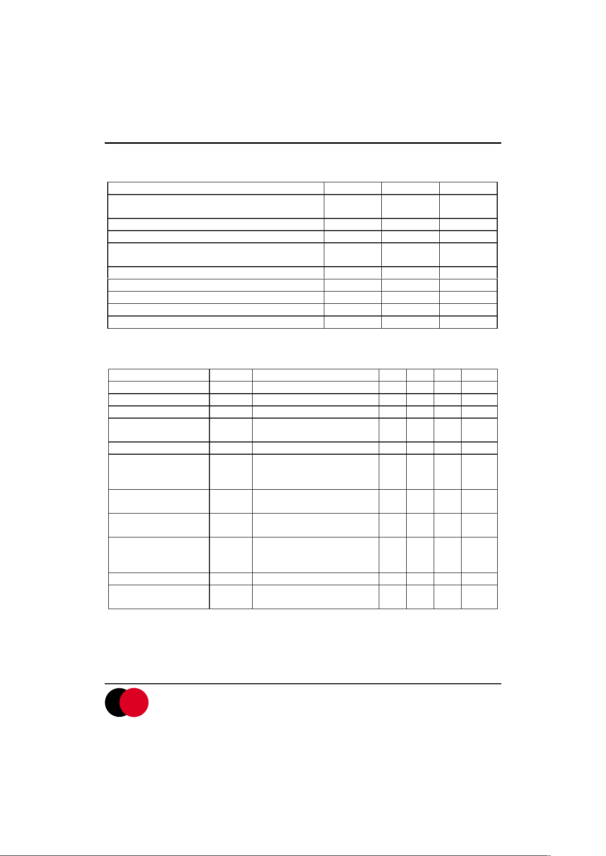
ABSOLUTE MAXIMUM RATINGS(Ta=25 C )
PARAMETER SYMBOL VALUE UNIT
Supply Voltage(between V+ and V-) Vcc 40 V
Pulse Voltage for 50ms Vpulse 50 V
Differential Input-Output Voltage Vd 40 V
Different Input Voltage (Between inverting and non-inverting
inputs)
Vid +-5 V
Different Input Voltage (Between Non-inverting Input and V-) Vid 8 V
Current from Zener Diode Terminal Iz 25 mA
Power Dissipation Pd 900 mW
Operating Temperature Topr -55 ~ 125 C
Storage Temperature Tstr -65 ~ 150 C
ELECTRICAL CHARACTERISTICS(Ta=25 C, V+=Vc=Vi=12V, Vo=5V, IL=1mA, C1=100Pf, Cref=0,
Rscp=0, unless otherwise specified, divider impedance R1*R2/(R1+R2) at non-inverting input, terminal 5=10K W)
PARAMETER SYMBOL TEST CONDITIONS MIN TYP MAX UNIT
Quiescent Regulator Current ICCQ IL=0, VI=30V 2.3 3.5 mA
Input Voltage Range VI 9.5 40 V
Output Voltage Range VO 2 37 V
Differential Input-Output
Voltage
VI-VO 3 38 V
Reference Voltage VREF 6.95 7.15 7.35 V
Line Regulation (note 1) DVO VI=12V to 40V
VI=12V to 15V
VI=12V to 15V, Ta=-55~125
C
0.02
0.01
0.2
0.1
%Vo
Load Regulation (note 1) DVO IL=1mA TO 50mA
IL=1mA TO 50mA,Ta=-55~125
C
0.03 0.15
0.6
%Vo
Output Voltage Temperature
Coefficient
DVO Ta=-55~125 C 0.002 0.015 %/ C
Ripple Rejection (note 2) RR f=50Hz to 10KHz
f=50Hz to 10KHz, Cref=5mF
Tmin<Ttyp<Tmax
74
86
2.5
dB
Short Circuit Limiting Current ILIM Rscp=10W, Vo=0 65 mA
Equivalent Noise RMS
output Voltage (note 2)
VN BW=100Hz to 10KHz, Cref=0
BW=100Hz to 10KHz, Cref=5mF
-20
2.5
mV
NOTE 1: Line and load regulation specifications are given for condit ions of a constant chip temperature. For
high dissipation condition, temperature drifts must be separately taken in account.
NOTE 2: For Cref, see Fig. 1
CONTEK
Contek Microelectronics Co.,Ltd.
http://www.contek-ic.com E-mail:sales@contek-ic.com
 Loading...