

Page 1

F&eIT Series
Isolated Digital Input/Output Module
DIO-16/16(FIT)GY
Isolated Digital Input Module
DI-32(FIT)GY
Isolated Digital Output Module
DO-32(FIT)GY
User’s Manual
CONTEC CO.,LTD.
Page 2

Check Your Package
Thank you for purchasing the CONTEC product.
The product consists of the items listed below.
Check, with the following list, t hat your packa ge is complete. If yo u discover dam aged or missi ng items,
contact your retailer.
Product Configuration List
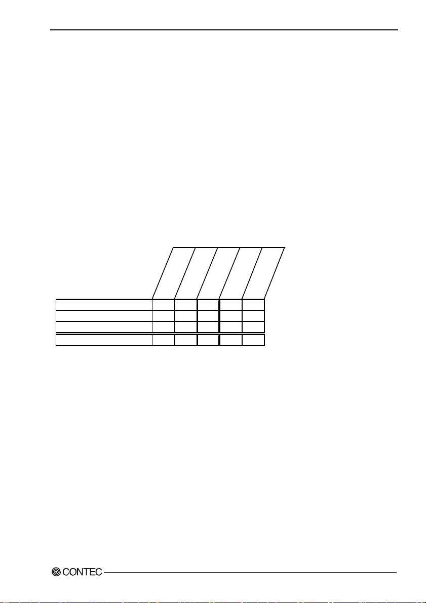
- Module (One of the following) ...1
[DIO-16/16(FIT)GY, DI-32(FIT)GY, or DO-32(FIT)GY]
- First Step Guide … 1
- CD-ROM[F&eIT Series Setup Disk] *1…1
- Interface connector plug ...1
*1 The CD-ROM contains various software and User’s Manual (this manual)
6
7
5
040
Device
4
1
ID
3
2
XY
C1
C0
C2
NC
00
00
01
01
02
02
03
03
04
04
05
05
06
06
07
07
10
10
11
11
12
12
13
13
14
14
15
15
16
16
17
17
DIO-16/16
Interface connector plug
Module
First step guide
CD-ROM
[F&eIT Series Setup Disk]
DIO-16/16(FIT)GY, DI-32(FIT)GY, DO-32(FIT)GY
i
Page 3

Copyright
Copyright 2004 CONTEC CO., LTD. ALL RIGHTS RESERVED.
No part of this document may be copied or reproduced in any form by any means without prior written
consent of CONTEC CO., LTD.
CONTEC CO., LTD. makes no commitment to update or keep c urre nt t he i n formation contained in this
document. The information in this document is subject to change without notice.
All relevant issues hav e be en consid e red in th e prep ar atio n of th is do cu men t. Sh ould yo u no tic e an
omission or any questionable item in this document, please feel free to notify CONTEC CO., LTD.
Regardless of the foregoing statement, CONTEC assumes no responsibility for any errors that may
appear in this document or for results obtained by the user as a result of using this product.
Trademarks
F&eIT is a registered trademark or trademark of CONTEC CO., LTD. Other company and product
names that are referred to in this manual are generally trademarks or registered trade trademark.
DIO-16/16(FIT)GY, DI-32(FIT)GY, DO-32(FIT)GY
ii
Page 4

Table of Contents
Check Your Packag e............................................................................................................................i
Copyright ............................................................................................................................................ii
Trademarks ......................................................................................................................................... ii
Table of Con tents...............................................................................................................................iii
1. Before Using the Product 1
About the Mo d ule............................................................................................................................... 1
Features........................................................................................................................................ 1
Functions...................................................................................................................................... 2
Functions and co n tro l meth o d by co nt ro ll e r co nn e c ted .............................................................. 3
Customer Supp o rt ............................................................................................................................... 5
Web Site....................................................................................................................................... 5
Limited One- Ye ar Wa rr a nt y............................................................................................................... 5
How to Obtain Serv i ce ....................................................................................................................... 5
Liability............................................................................................................................................... 5
Safety Precau t io ns .............................................................................................................................. 6
Safety Infor mat i o n .......................................................................................................................6
Handling Pre ca u tio ns................................................................................................................... 6
Environment................................................................................................................................. 9
Inspection..................................................................................................................................... 9
Storage ......................................................................................................................................... 9
Disposal ....................................................................................................................................... 9
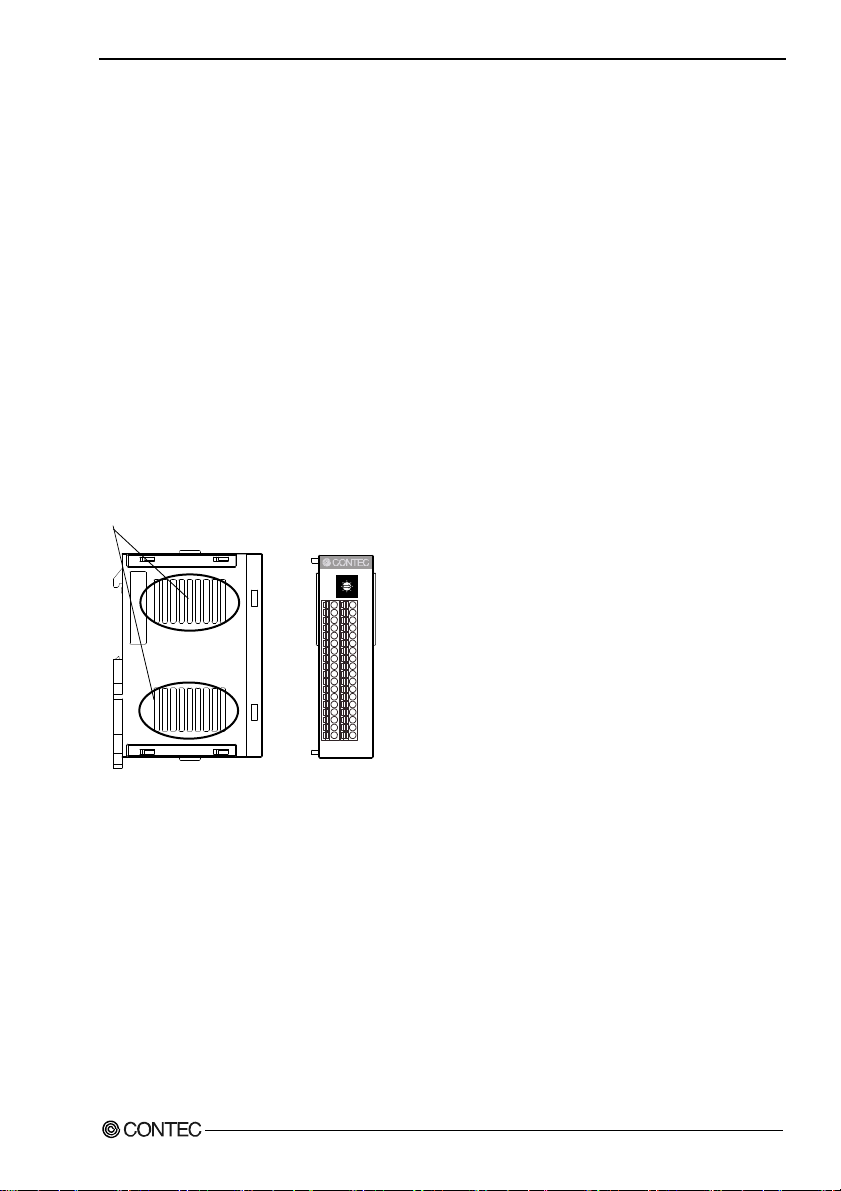
2. Module Nomenclature and Settings 11
Nomenclature of Module Components............................................................................................ 11
Setting a Dev ic e ID........................................................................................................................... 12
Setup Method................................................................................................................... .......... 12
3. Connecting to an External Device 13
Interface Con n ec to r .......................................................................................................................... 13
How to Connect an Interface Connector ................................................................................... 13
Signal Layout on the Interface Connector................................................................................. 14
External I/O C i r cu it s......................................................................................................................... 17
Surge Voltage Co u nt e r mea su r es ...................................................................................................... 20
4. Using the I/O Address Map 21
Starting I/O Ad d r es s ......................................................................................................................... 21
List of I/O Add re s s Ma p s ................................................................................................................. 22
DIO-16/16(FIT)GY, DI-32(FIT)GY, DO-32(FIT)GY
iii
Page 5

Specificatio ns Co mmo n to F &e IT P ro du c ts.....................................................................................29
Product Info r mat i on................................................................................................................... 29
Interrupt Con t ro l Fu n ct io n......................................................................................................... 31
Digital Filter (Hardware).................................................................................................................. 35
Digital Filter Operation Principle..............................................................................................35
Data I/O Oper ati o ns th at D i re ct ly Ac c es s a n I/O Po r t .....................................................................37
Data Input................................................................................................................................... 37
Data Output................................................................................................................................ 38
Monitoring th e O utp u t D a ta ....................................................................................................... 39
Examples........................................................................................................................................... 40
Software Mod e........................................................................................................................... 40
5. Using the Memory Address Map 41
DIO-16/16(FIT)GY .......................................................................................................................... 42
Module Infor ma ti o n Are a ..........................................................................................................42
Module Infor ma ti o n Are a ..........................................................................................................45
Basic I/O Data Ar ea................................................................................................................... 46
DI-32(FIT)GY...................................................................................................................................47
Module Infor ma ti o n Are a ..........................................................................................................47
Module Infor ma ti o n Are a ..........................................................................................................50
Basic I/O Data Ar ea................................................................................................................... 51
DO-32(FIT)G Y .................................................................................................................................52
Module Infor ma ti o n Are a ..........................................................................................................52
Module Infor ma ti o n Are a ..........................................................................................................55
Basic I/O Data Ar ea................................................................................................................... 56
Examples........................................................................................................................................... 57
6. System Reference 61
Circuit Block Di a gr a m < DI O -16 /1 6 (F I T) GY > .............................................................................61
Specificatio ns < DI O -1 6/ 16 ( F IT )G Y > ...........................................................................................62
Circuit Block Di a gr a m < DI -3 2 (F I T) GY > .....................................................................................64
Specificatio ns < DI -3 2 (F IT )G Y > ...................................................................................................65
Circuit Block Di a gr a m < DO -3 2 (F I T) G Y > ................................................................................... 67
Specificatio ns < DO -3 2 (F IT )G Y > .................................................................................................68
External Dime ns i on s......................................................................................................................... 70
DIO-16/16(FIT)GY, DI-32(FIT)GY, DO-32(FIT)GY
iv
Page 6

1. Before Using the Product
1. Before Using the Product
This chapter provides information you should know before using the product.
About the Module
This product is an expansion module (device module) that adds digital signal I/O interfaces to one of
various types of controllers. The product is used in combination with the I/O controller module
< CPU-CAxx(FIT)GY > (*1) or BOX-PC < BX-300-DC5xxx > (*1) or microcontroller unit
< CPU-SBxx(FIT)GY > (*1) in the F&eIT Series.
The < DIO-16/16(FIT)GY > can perform a maximum of 16 points of opto-isolated input and 16 points of
opto-isolated output per module. (Input: 12 - 24 VDC specified, output: 12 - 48 VDC specified)
The < DI-32(FIT)GY > can perform a m a ximum of 32 points of opto-isolated i np ut per m odule. (In p ut:
12 - 24 VDC specified)
The < DO-32(FIT)GY > can perform a maximum of 32 points of opto-isolated output per module.
(Output: 12 - 48 VDC specified)
By reading this manual carefully, please build a system by creating applications programs, setting the
switches, and connecting the module to external devices.
*1 This module is available in different product models. "x" in each model number represents a
blank or one alphanumeric character. This is applicable to the rest of this document.
Features
- A different external power supply can be used for each common pin as it is shared by 16 signal
points.
- The < DIO-16/16(FIT)GY > can perform 16-points digital signal input and 16-points digital signal
output.
- < DI-32(FIT)GY > can perform 32-points digital signal input.
- < DO-32(FIT)GY > can perform 32-points digital signal output.
- The output section is a high sink current, open collector type using high-capacitance transistors.
< DIO-16/16(FIT)GY >: 150 mA/24 VDC or 50 mA/48 VDC max. (per channel)
< DO-32(FIT)GY >: 150 mA/24 VDC or 50 mA/48 VDC max. (per channel))
- Input section is ready to accept both the current sinking output and current source output.
- Isolated I/O operations using an optocoupler improves noise immunity.
- The card has a digital filter to prevent input signals from carrying noise or a chattering.
- A rotary switch allows you to set device IDs, making it easy to keep track of device nu mbers.
- Like other F&eIT series products, the module has a 35mm DIN rail mounting mechanism as
standard. A connection to a controller module can be effected on a lateral, stack basis in a unique
configuration, which perm its a sim ple, sm art sy stem confi gura tion wi thout t he need for a bac kplane
board.
- You can use all of the input signals as interrupt in puts. You can al so select the i nterrupt tri gger edge
of the input signal.
DIO-16/16(FIT)GY, DI-32(FIT)GY, DO-32(FIT)GY
1
Page 7

1. Before Using the Product
Functions
Generic I/O functions (data I/O operations that directly access the I/O ports)
- Input
The Module transmits a maximum of 32 points (< DI-32(FIT)GY >) or 16 points
(< DIO-16/16(FIT)GY >) of externally supplied digital signals to a controller module that is connected
to it. Access to the Module from a controller module is performed through the input port that is
specified by means of a Device ID. When an input port is read by the execution of an input command,t
he buffer gate associated with the input port is opened, and the digital signals supplied from an
external device are fetched in groups. During this operation, if the module is the DI-32(FIT)GY,
DIO-16/16(FIT)GY, signals that are transmitted to the controller module will be [ON (closed): 1, OFF
(open): 0].
- Output
The Module writes a maximum of 32 poi nts (< DO-32(FIT)GY >) or 16 points (< DIO-16/16(FIT)GY >)
of digital signals to an external device. Access to the Module from a controller module is performed
through the output port that is specified by means of a Device ID. When data is written to the output port
by the execution of an output command, the data is held on the latch circuit that is associated with the
output port. After being electrically isolated by an optocoupler, if the module is the DO-32(FIT)GY,
DIO-16/16(FIT)GY, the digital signals are transmitted to the connected external device through
transistors. During this operation, signals that are transmitted to the external device will be [ON
(closed): 1, OFF (open): 0].
Output data monitoring function
This function allows you to keep track of the signal data that is being output.
DIO-16/16(FIT)GY, DI-32(FIT)GY, DO-32(FIT)GY
2
Page 8
1. Before Using the Product
Y
Y
Y
Functions and control method by controller connected
The DIO-16/16(FIT)GY, DI-32(FIT)GY, and DO-32(FIT)GY can be connected to a variety of
controllers.
Supported controllers
BOX-PC : BX-300-DC5xxx
Microcontroller Unit : CPU-SBxx(FIT)GY
I/O Controller Module : CPU-CAxx(FIT)GY
Monitoring & Control Server Unit : SVR-MMF2(FIT)
Check each controller to which the module can be connected as well as the method of controlling the
module when conn ec ted to th at co nt ro ll er .
Connections to controllers
G
)
x
T
x
I
x
F
5
(
C
x
x
x
D
-
0
O: Permitted
: Not permitted
×
DIO- 16/1 6(FIT)GY
DI-32(FIT)GY
DO-32(FIT) GY
Device ID setting range 0 - 70 - 70 - 70 - 70 - 7
0
3
-
X
B
ٛٛٛٛ ×
ٛٛٛٛ ×
ٛٛٛٛ ×
A
B
S
C
-
-
U
U
P
P
C
C
)
G
)
T
I
F
(
x
M
M
-
R
V
S
G
)
T
I
T
I
F
(
F
(
2
F
F
M
M
-
R
V
S
DIO-16/16(FIT)GY, DI-32(FIT)GY, DO-32(FIT)GY
3
Page 9
1. Before Using the Product
Y
Y
Y
Control method by co n tro lle r co n nec te d
)
x
x
x
5
C
D
-
0
S
-
0
3
U
P
X
C
Control using the I/O address map
Control using the memory address map
Control via the Windows driver * FIT Protocol
API -CAP (W32)
API-SBP(W32)
API-USBP(WDM)
Control over the web
(as set from within the browser)
* The API-SBP(W32) is included in the development kit [DTK-SBxx(FIT)GY]; the other drivers are bundled with each
controller.
B
ٛٛ
ٛٛ
T
T
I
I
F
F
(
(
x
x
x
x
B
M
A
C
M
-
-
U
R
P
V
C
S
ٛ
ٛ
ٛ
ٛ
G
G
)
)
G
)
T
I
T
I
F
(
F
(
2
F
F
M
M
-
R
V
S
Control using the I/O address map
When connected to the BX-300-DC5xxx, the CPU-SBxx(FIT)GY, the module can receive I/O
instructions directly from the controller module. For details, see Chapter 4 “Using the I/O Address
Map”.
Control using the memory address map
When connected to the CPU- CAxx ( FI T)G Y, th e mod ule can be accessed from the host computer over
the network. The module is assigned with its device ID in the memory managed by the controller
module. The application running on the host computer controls the module by reading/writing the
memory managed by the controller module. For details, see Chapter 5 “Using the Memory Address
Map”.
Control via the Windows driver
For the functions and settings available when using the Windows driver, refer to the reference manual
and online help for each module.
Control over the web
Control over the web – Connecting to the SVR-MMF2(FIT)
You can monitor collected data and manage the log over t he w eb. You can use your familiar browser to
easily make various settings. For details, refer to the reference manual for the SVR-MMF2(FIT).
DIO-16/16(FIT)GY, DI-32(FIT)GY, DO-32(FIT)GY
4
Page 10

1. Before Using the Product
Customer Support
CONTEC provides the following s upport services fo r you to use CONTEC products more efficiently and
comfortably.
Web Site
Japanese http://www.contec.co.jp/
English http://www.contec.com/
Chinese http://www.contec.com.cn/
Latest product information
CONTEC provides up-to-date information on products.
CONTEC also provides product manuals and various technical documents in the PDF.
Free download
You can download updated driver software a nd diff erenti al files as we ll as sample pr ograms available i n
several languages.
Note! For product information
Contact your retailer if you have any technical question about a CONTEC product or need its price,
delivery time, or estimate information.
Limited One-Year Warranty
CONTEC F&eIT products are warranted by CONTEC CO., LTD. to be free from defects in material and
workmanship for up to one year from the date of purchase by the original purchaser.
Repair will be free of char ge only w hen thi s device is ret urned fr eight pr epaid with a c opy of t he origi nal
invoice and a Return Merchandise Authorization to the distributor or the CONTEC group office, from
which it was purchased.
This warranty is not applicable for scratches or normal wear, but only for the electronic circuitry and
original products. The warranty is not applicable if the device has been tampered with or damaged
through abuse, mistreatment, neglect, or unreasonable use, or if the original invoice is not included, in
which case repairs will be considered beyond the warranty policy.
How to Obtain Service
For replacement or repair, return the device freight prepaid, with a copy of the original invoice. Please
obtain a Return Merchandise Authorization number (RMA) from the CONTEC group office where you
purchased before returning any product.
* No product will be accepted by the CONTEC group without the RMA number.
Liability
The obligation of the warrantor is solely to repair or replace the product. In no event will the warrantor
be liable for any incidental or consequential damages due to s uch defec t or consequence s that arise from
inexperienced usage, misuse, or malfunction of this device.
DIO-16/16(FIT)GY, DI-32(FIT)GY, DO-32(FIT)GY
5
Page 11
1. Before Using the Product
Safety Precautions
Understand the following definitions and precautions to use the product safely.
Safety Information
This document provides safety information u sing the foll owing sym bols to prevent a ccidents res ulting in
injury or death and the destruc tion of equi pment and res ources. Under stand the mean ings of these la bels
to operate the equipment safely.
DANGER
WAR NI NG
CAUTION
DANGER indicates an imminently hazardous situation which, if not avoided, will
result in death or serious injury.
WARNING indicates a potentially hazardous situation which, if not avoided, could
result in death or serious injury.
CAUTION indicates a potentially hazardous situation which, if not avoided, may
result in minor or moderate injury or in property damage.
Handling Precautions
CAUTION
- Do not modify the module. CONTEC will bear no responsibility for any problems, etc., resulting
from modifying this module.
- Do not use or store the module in a hot or cold place, or in a place that is subject to severe
temperature changes.
(Operating temperature range: 0 - 50°C)
- Do not use or store the module in a place subject to direct sunlight or near a heating device, such as
a stove.
- Do not use or store the module in a dusty or humid place.
(Operating humidity range: 10 - 90%RH, No cond ens ation )
- As this module contains precision electronic components, do not use or store it in environments
subject to shock or vibration.
- Do not use or store the module near equipment generating a strong magnetic field or radio waves.
- If you notice any strange odor or overheating, please unplug the power cable immediately.
- In the event of an abnormal condition or malfunction, please consult the dealer from whom the
module was purch as ed .
- To avoid electric shock, please do not touch the module with a wet hand.
- Do not open the module casing. CONTEC will disclaim any resp onsibility for module whose casi ng
has been opened.
- Do not strike or bend the module. Doing so could damage the module.
- To prevent contact malfunction, please do not touch the metallic pins on the external module
connector.
DIO-16/16(FIT)GY, DI-32(FIT)GY, DO-32(FIT)GY
6
Page 12
1. Before Using the Product
r
Q
y
r
Q
y
r
Q
y
- The module contains switches that need to be properly set. Before using the module, please check
its switch settings.
- To avoid malfunction, please do not change the module switch settings in an unauthorized manner.
- Do not connect the device module to the controller module alrea dy energized. T o avoid ma lfunction,
please be sure to turn off the control module before connecting the device module to it.
- Regarding “CE EMC Directive Class A Notice”
The ferrite core must be installed in a digital-input/output interface connecting cable so that this
product may suit the above-mentioned standard.
DIO-16/16(FIT)GY
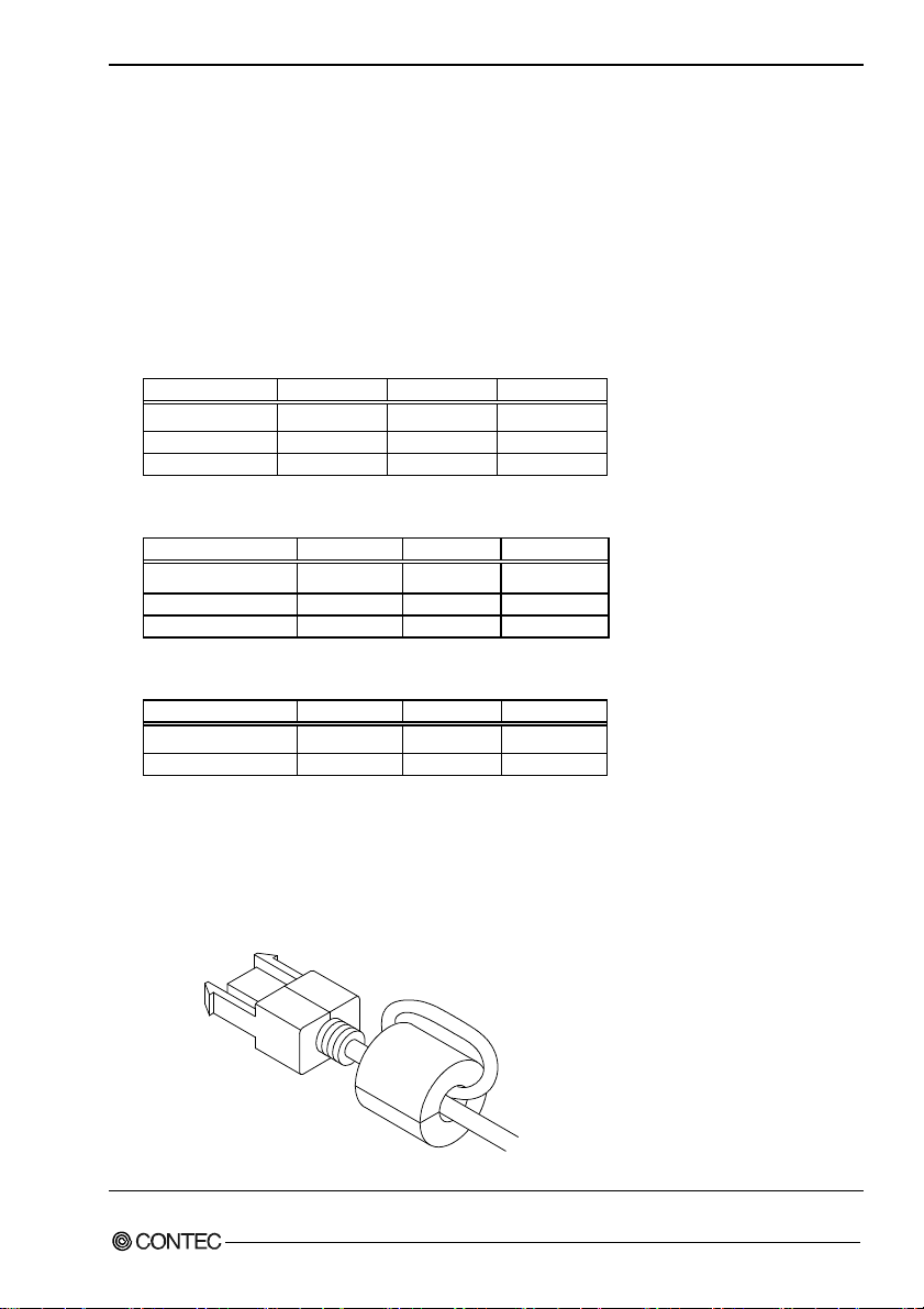
Name Make
E04SS251512 SEIWA 2 2
E04SR301334 SEIWA 2 3
E04SS231114 SEIWA 2 1
DI-32(FIT)GY
Name Make
E04SF440350127 SEIWA 1 1
E04SS251512 SEIWA 1 1
E04SR301334 SEIWA 1 1
DO-32(FIT)GY
Name Make
E04SF360270127 SEIWA 1 2
E04SS251512 SEIWA 1 1
When attaching a ferrite core to the cable, coil it around figure several times fromonce near the
connector while leaving it open, and then close it.
Reference: When twisting around a USB cable once
Turn
Turn
Turn
uantit
uantit
uantit
DIO-16/16(FIT)GY, DI-32(FIT)GY, DO-32(FIT)GY
7
Page 13

1. Before Using the Product
FCC PART 15 Class A Notice
NOTE
This equipment has been tested and found to comply with the limits for a Class A digital
device, pursuant to part 15 of the FCC Rules. These limits are designed to provide reasonable
protection against harmful interference when the equipment is operated in commercial
environment.
This equipment generates, uses, and can radiate radio frequency energy and, if not installed
and used in accordance with the instruction manual, may cause harmful interference to radio
communications. Operation of this equipment in a residential area is likely to cause harmful
interference at his own expense.
WAR NIN G TO USE R
Change or modifications not expressly approved the manufacturer can void the user's
authority to operate this equipment.
DIO-16/16(FIT)GY, DI-32(FIT)GY, DO-32(FIT)GY
8
Page 14
1. Before Using the Product
Environment
Use this product in the following environm ent. If used in an u nauthorize d environm ent, the module m ay
overheat, malfunction, or cause a failure.
Operating temperature
0 - 50°C
Operating humidity
10 - 90%RH (No condensation)
Corrosive gases
None
Floating dust particles
Not to be excessive
Inspection
Inspect the product periodically as follows to use it safely.
- Check that the ventilation slit has no obstruction and
has no dust or foreign matter adhering.
6
7
5
040
Device
4
1
3
ID
2
XY
C1
C0
C2
NC
00
00
01
01
02
02
03
03
04
04
05
05
06
06
07
07
10
10
11
11
12
12
13
13
14
14
15
15
16
16
17
17
DIO-16/16
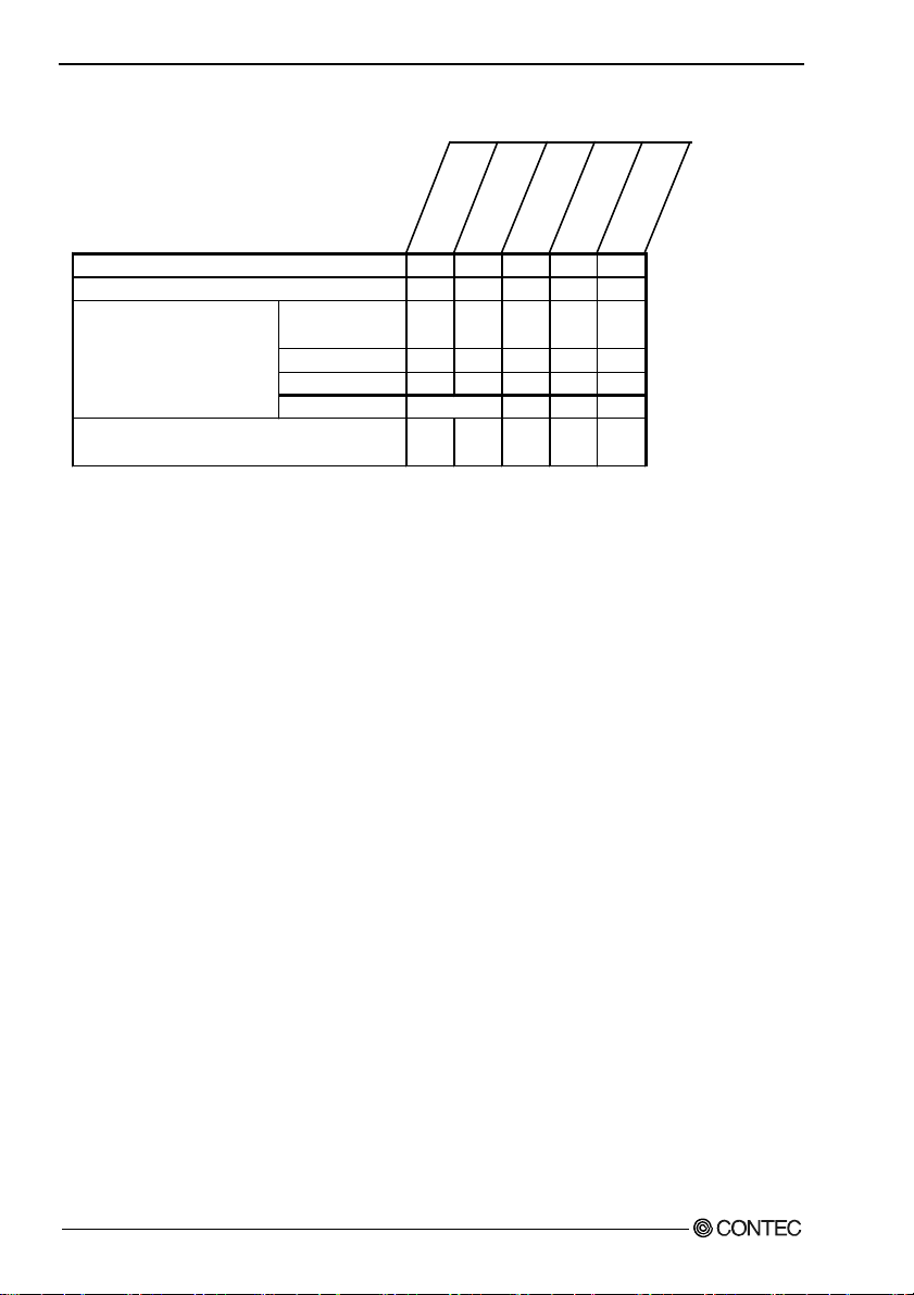
* The above figure is the DIO-16/16(FIT)GY but
it is the same with the DI-32(FIT)GY and
DO-32(FIT)GY.
Storage
When storing this product, keep it in its original packing fo rm.
(1) Put the module in the storage bag.
(2) Wrap it in the packing material, then put it in the box.
(3) Store the package at room temperature at a place free from direct sunlight, moisture, shock,
vibration, magnetism, and static electricity.
Disposal
When disposing of the product, follow the disposal procedures stipulated under the relevant laws and
municipal ordinances.
DIO-16/16(FIT)GY, DI-32(FIT)GY, DO-32(FIT)GY
9
Page 15

1. Before Using the Product
DIO-16/16(FIT)GY, DI-32(FIT)GY, DO-32(FIT)GY
10
Page 16
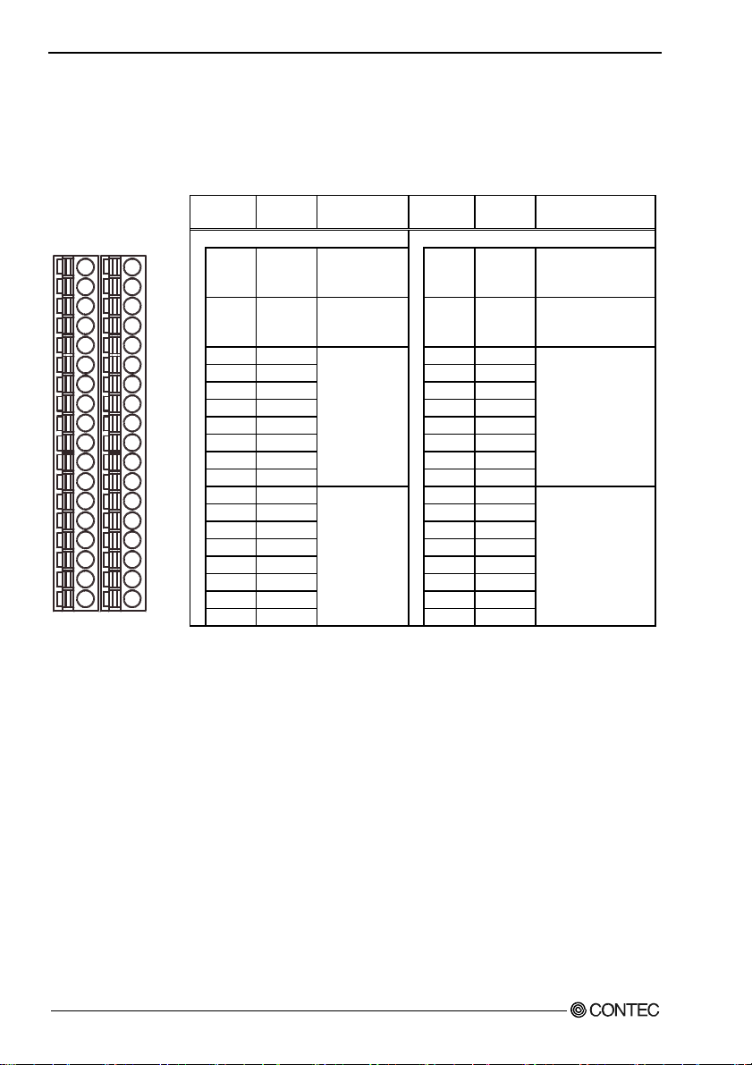
2. Module Nomenclature and Settings
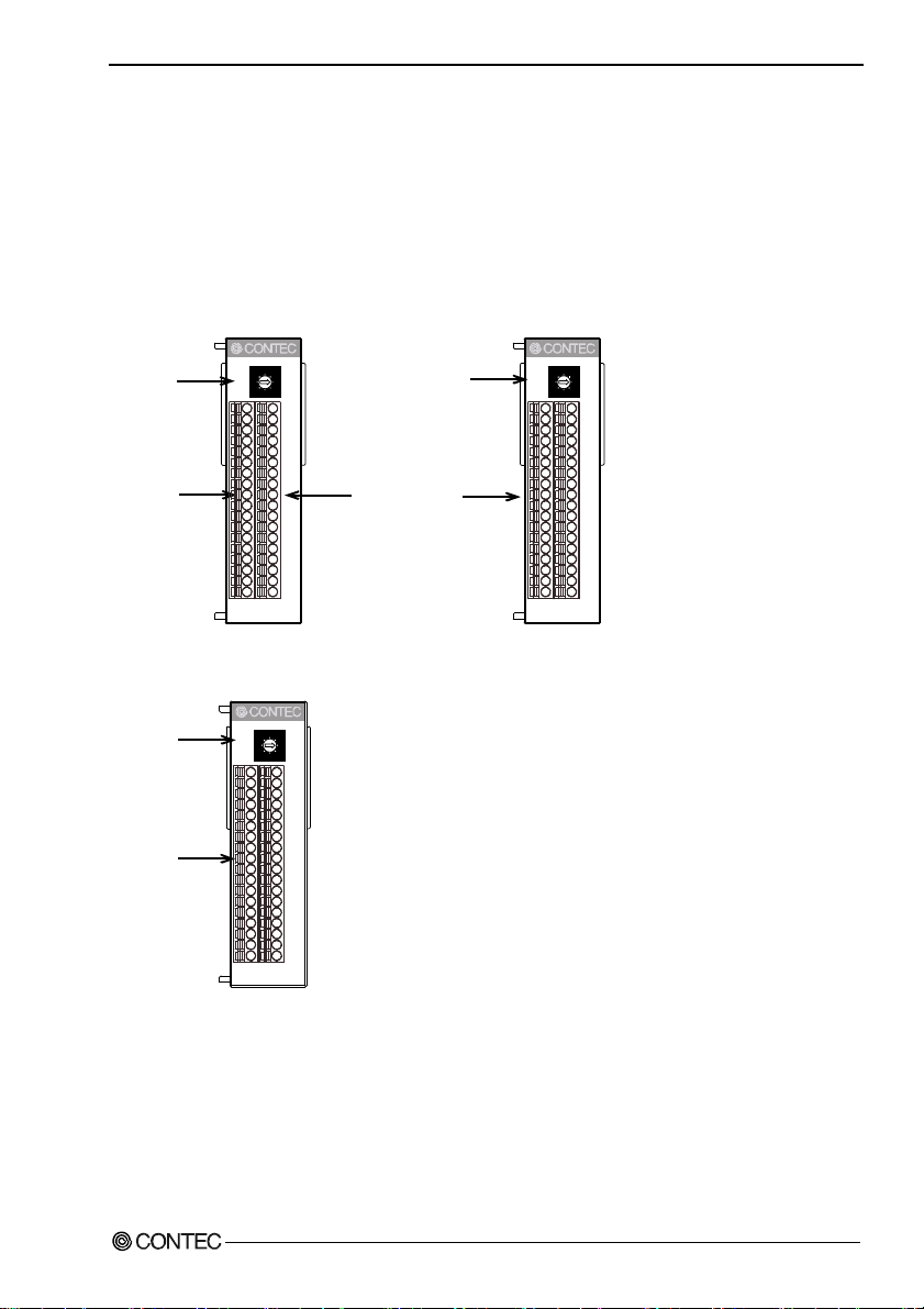
2. Module Nomenclature and Settings
Nomenclature of Module Components
Figure 2.1 shows the names of module components.
In the figure, the indicated switch settings represent factory settings.
DIO-16/16(FIT)GY DI-32(FIT)GY
Device ID
Input
Device
040
4
1
3
ID
2
XY
C0
C1
NC
C2
00
00
01
01
02
02
03
03
04
04
05
05
06
06
07
07
10
10
11
11
12
12
13
13
14
14
15
15
16
16
17
17
Output
Device ID
Input
6
7
5
DIO-16/16
DO-32(FIT)GY
6
7
Device ID
Output
Device
ID
5
4
3
DO-32
040
1
2
Y
C0
C2
C1
C3
00
20
01
21
02
22
03
23
04
24
05
25
06
26
07
27
10
30
11
31
12
32
13
33
14
34
15
35
16
36
17
37
Figure 2.1. Names of Module Components
Device
6
7
5
040
4
1
3
ID
2
X
C0
C1
NC
NC
00
20
01
21
02
22
03
23
04
24
05
25
06
26
07
27
10
30
11
31
12
32
13
33
14
34
15
35
16
36
17
37
DI-32
DIO-16/16(FIT)GY, DI-32(FIT)GY, DO-32(FIT)GY
11
Page 17
2. Module Nomenclature and Settings
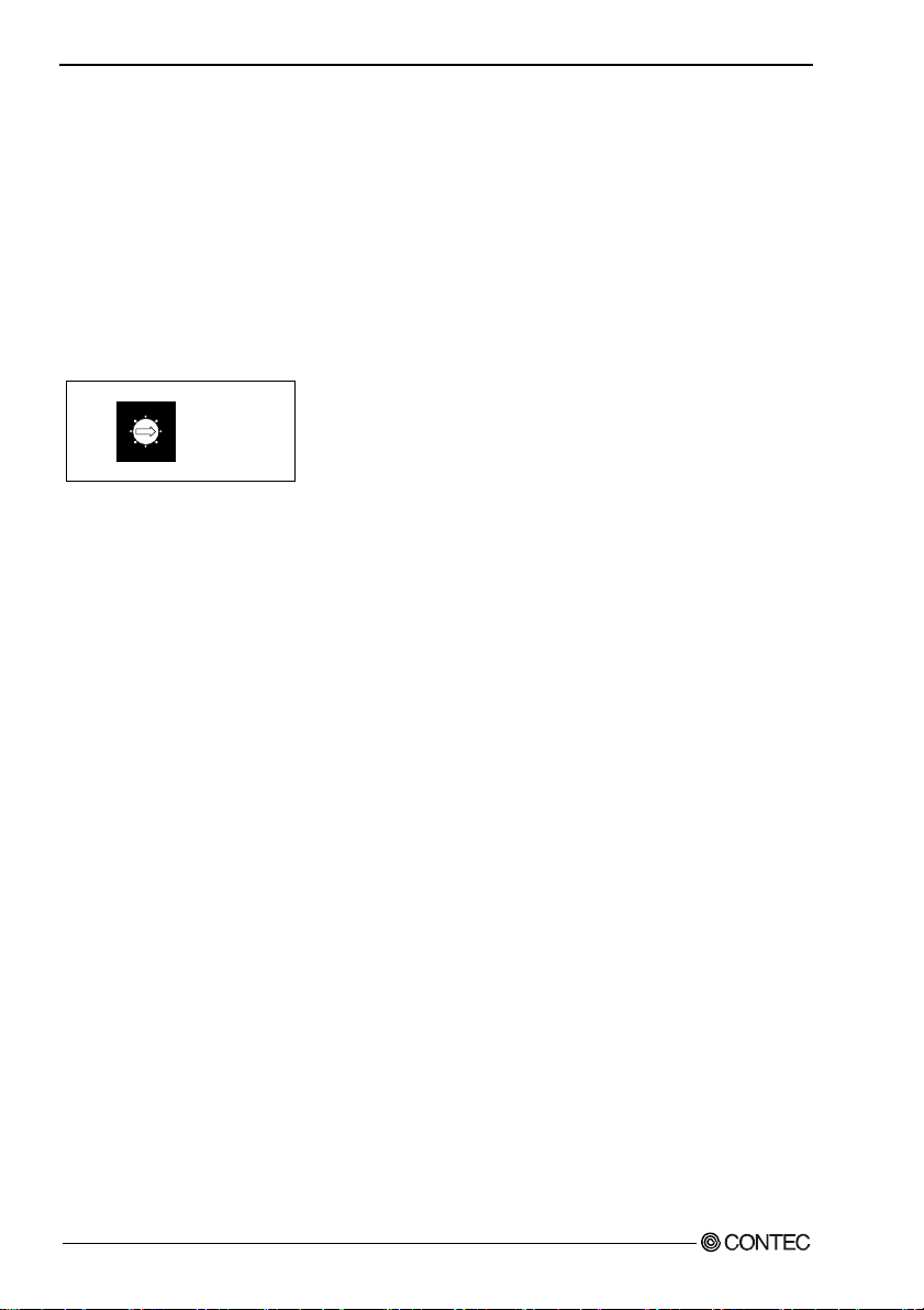
Setting a Device ID
The controller module distinguishes and keeps track of the modules that are c onnecte d to it by ass igning
device IDs to them. Each module, therefore, should be assigned a unique ID.
A Device ID can be assigned in a 0 - 7 range, so t hat a m a ximum of eight modules can be distinguis hed.
The factory setting for the Device ID is [0].
Setup Method
A Device ID can be set by turning the rotary switch that is located on the module face.
A Device ID can be assigned by turning the switch.
6
7
5
4
3
2
040
1
Factory setting:
(Device ID = 0)
Device
ID
Figure 2.2. Setting a Device ID
DIO-16/16(FIT)GY, DI-32(FIT)GY, DO-32(FIT)GY
12
Page 18
3. Connecting to an External Device
3. Connecting to an External Device
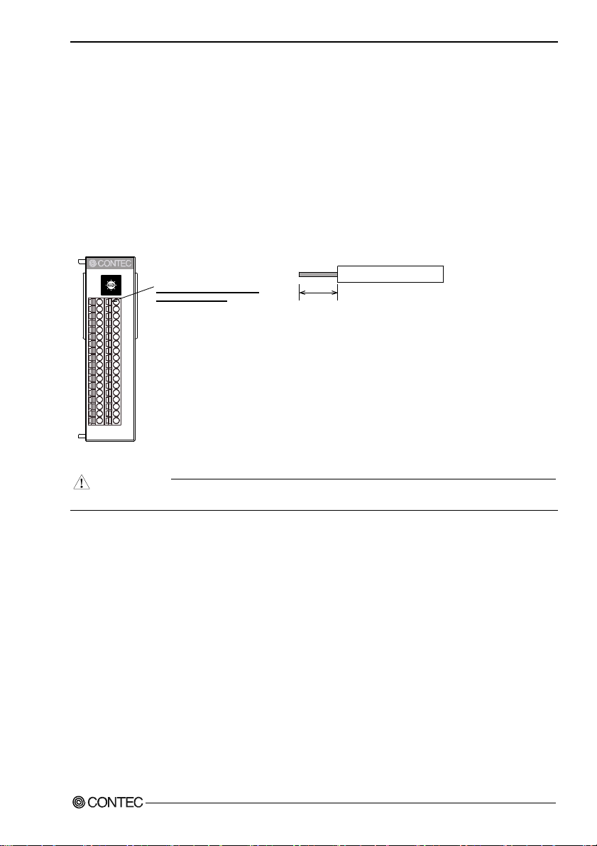
Interface Connector
How to Connect an Interface Connector
When connecting the Module to an external device, you can use the supplied connector plug.
When wiring the Module, strip off approximately 9 - 10mm of the covering for the cable, and insert the
bare wire by pressing the orange button on the connector plug. Releasing the orang e button af ter the
wire is inserted fixes the cable. Compatible wires are AWG 24 - 16.
6
7
5
040
Device
4
1
3
ID
DIO-16/16
Figure 3.1. Connecting an Interface Connector and Connectors That Can Be Used
CAUTION
Removing the connector plug by grasping the cable can break the wire.
Push this section to insert
2
XY
the wire material.
C0
C1
NC
C2
00
00
- Connector used:
01
01
02
02
03
03
04
04
05
05
06
06
07
07
10
10
11
11
12
12
13
13
14
14
15
15
16
16
17
17
3.5mm pitch, 36-pin type, 6.0A rated current
MCDN1, 5 /18-G1-3, 5P26THR [made by Phoenix Contact Corp.]
- Applicable plug (bundled):
Front screw type with connector stopper flange
FMC1, 5/ 18-ST-3, 5 [made by Phoenix Cont act Corp.]
Applicable cable: AWG24-16
9 - 10mm
DIO-16/16(FIT)GY, DI-32(FIT)GY, DO-32(FIT)GY
13
Page 19
3. Connecting to an External Device
Signal Layout on the Interface Connector
The Module can be connected to an external device using two 18-pin connectors that is provided on the
Module face.
DIO-16/16(FIT)GY
NC
Pin No.
X Y
XY
C0
C1
C2
00
00
NC N.C. Unconnected C2 COM(-)
01
01
02
02
00 IN00 00 OUT00
03
03
01 IN01 01 OUT01
04
04
02 IN02 02 OUT02
05
05
03 IN03 03 OUT03
06
06
04 IN04 04 OUT04
05 IN05 05 OUT05
07
07
06 IN06 06 OUT06
10
10
07 IN07
11
11
10 IN10 10 OUT10
12
12
11 IN11 11 OUT11
13
13
12 IN12 12 OUT12
14
14
13 IN13 13 OUT13
15
15
14 IN14 14 OUT14
16
16
15 IN15 15 OUT15
17
17
16 IN16 16 OUT16
17 IN17
Signal
name
C0 COM
Meaning Pin No.
Connmon for
Input+0, +1
group
Input+0 group
Input+1 group
C1 COM(+)
07 OUT07
17 OUT17
Figure 3.2. Signal Layout on the Interface Connector < DIO-16/16(FIT)GY >
Signal
name
Meaning
Plus connmon for
Output+0, +1
group
Minus connmon for
Output+0, +1
group
Output+0 group
Output+1 group
DIO-16/16(FIT)GY, DI-32(FIT)GY, DO-32(FIT)GY
14
Page 20
3. Connecting to an External Device
DI-32(FIT)GY
C0
NC
00
01
02
03
04
05
06
07
10
12
13
14
15
16
17
Pin No.
X
C1
X X
NC
20
21
22
23
24
25
26
27
30
11
31
32
33
34
35
36
37
Signal
name
C0 COM
NC N.C. Unconnected NC N.C. Unconnected
00 IN00 20 IN20
01 IN01 21 IN21
02 IN02 22 IN22
03 IN03 23 IN23
04 IN04 24 IN24
05 IN05 25 IN25
06 IN06 26 IN26
07 IN07
10 IN10 30 IN30
11 IN11 31 IN31
12 IN12 32 IN32
13 IN13 33 IN33
14 IN14 34 IN34
15 IN15 35 IN35
16 IN16 36 IN36
17 IN17
Meaning Pin No.
Connmon for
Input+0, +1
group
Input+0 group
Input+1 group
Signal
name
C1 COM
27 IN27
37 IN37
Meaning
Connmon for
Input+2, +3
group
Input+2 group
Input+3 group
Figure 3.3. Signal Layout on the Interface Connector < DI-32(FIT)GY >
DIO-16/16(FIT)GY, DI-32(FIT)GY, DO-32(FIT)GY
15
Page 21
3. Connecting to an External Device
DO-32(FIT)GY
Pin No.
Y
Y Y
C0
C2
C1
C3
00
20
01
21
C1 COM(-)
02
22
03
23
00 OUT00 20 OUT20
04
24
01 OUT01 21 OUT21
02 OUT02 22 OUT22
05
25
03 OUT03 23 OUT23
06
26
04 OUT04 24 OUT24
07
27
05 OUT05 25 OUT25
10
30
06 OUT06 26 OUT26
11
31
07 OUT07
12
32
10 OUT10 30 OUT30
13
33
11 OUT11 31 OUT31
14
34
12 OUT12 32 OUT32
15
35
13 OUT13 33 OUT33
14 OUT14 34 OUT34
16
36
15 OUT15 35 OUT35
17
37
16 OUT16 36 OUT36
17 OUT17
Signal
name
C0 COM(+)
Meaning Pin No.
Plus connmon
for Output+0,
+1 group
Minus connmon
for Output+0,
+1 group
Output+0
group
Output+1
group
C2 COM(+)
C3 COM(-)
27 OUT27
37 OUT37
Signal
name
Meaning
Plus connmon for
Output+2, +3
group
Minus connmon
for Output+2, +3
group
Output+2 group
Output+3 group
Figure 3.4. Signal Layout on the Interface Connector < DO-32(FIT)GY >
DIO-16/16(FIT)GY, DI-32(FIT)GY, DO-32(FIT)GY
16
Page 22
3. Connecting to an External Device
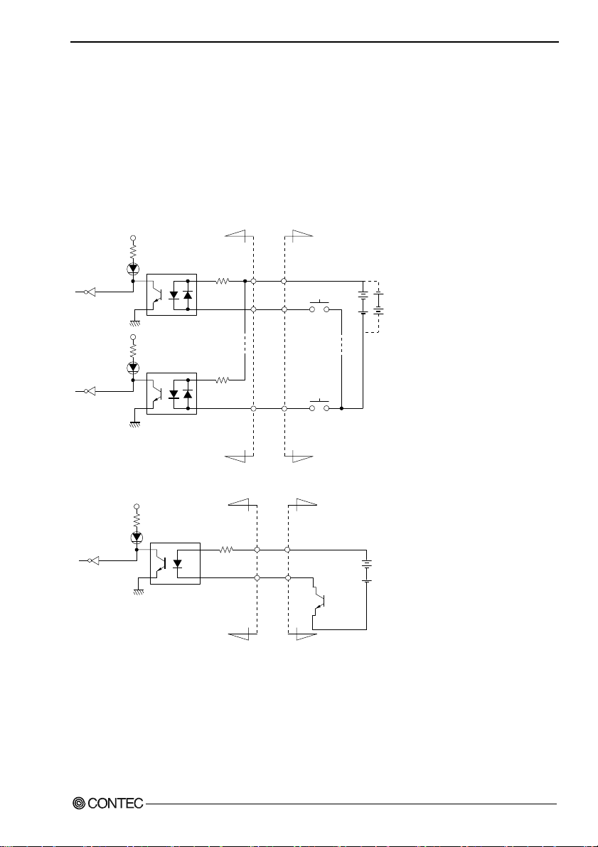
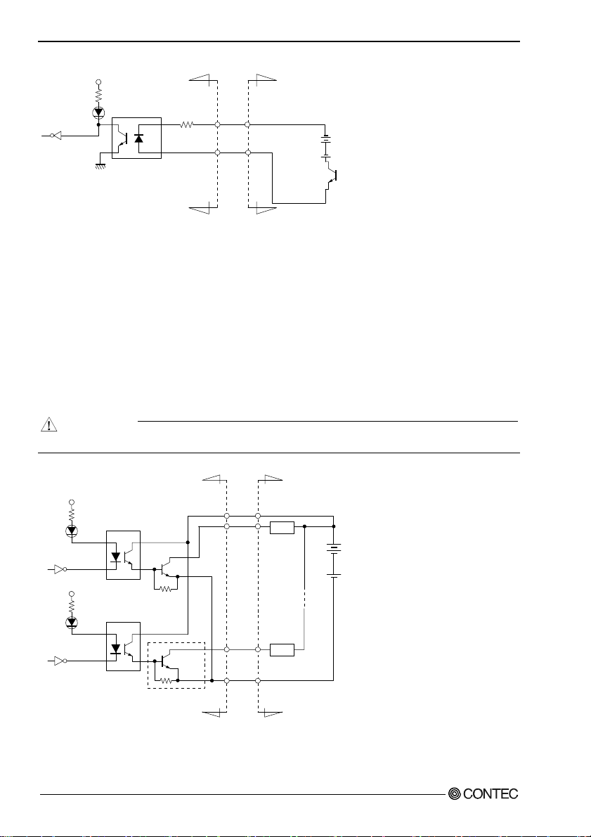
External I/O Circuits
Input section < DIO-16/16(FIT)GY >, < DI-32(FIT)GY >
Figure 3.5 shows the input equivalent c ircuit for t he interfac e section of the < DIO- 16/1 6(FIT)GY > a nd
< DI-32(FIT)GY >.
The signal input section consists o f an opto-i solate d inpu t (com patible wi th both c urre nt sink ou tput a nd
current source output). An external power s upp ly is th erefore requ ired to driv e the inpu t section of this
module. The power requirement for t he < DIO-16/16(FIT) GY > or < DI-32(FIT) GY > is about 8 mA per
input channel at 24 VDC (about 4 mA at 12 VDC).
External circuitModule
Vcc
3kΩ
Optocoupler
Optocoupler
3kΩ
+/-
common
Input
pin
Input
pin
Input contact
point
Input contact
point
External
power supply
12V - 24VDC
Figure 3.5. Input Circuit < DIO-16/16(FIT)GY >, < DI-32(FIT)GY >
External circuitModule
Vcc
3kΩ
Optocoupler
Plus
common
Input
pin
Current sink
output
External
power supply
12V - 24VDC
Figure 3.6. Example of a Connection to Current Sink Output
< DIO-16/16(FIT)GY >, < DI-32(FIT)GY >
DIO-16/16(FIT)GY, DI-32(FIT)GY, DO-32(FIT)GY
17
Page 23
3. Connecting to an External Device
External circuitModule
Vcc
3kΩ
Optocoupler
common
Input
pin
External
power supply
Current
source output
Figure 3.7. Example of a Connection to Current Source Output
< DIO-16/16(FIT)GY >, < DI-32(FIT)GY >
Output section
Figure 3.8 shows the output circuit for the interface section of the < DIO-16/16(FIT)GY > and
< DO-32(FIT)GY >. The signal output section consists of an opto-isolated open collector output
(current sink type). An external power supply is therefore required to drive the output section of this
module.
The maximum output current rating per channel is 150 mA for the < DIO-16/16(FIT)GY > or
< DO-32(FIT)GY > (at 12 - 24 VDC) or 50 mA for the < DIO-16/16(FIT)GY > or < DO-32(FIT)GY >
(at 36 - 48 VDC). A surge voltage protection circuit (zener diode) is provided for the output transist ors
of this module. When the module drives relays, lamps, and other indu ction lo ad s, however, an other
surge voltage countermeasure should be provided on the load side.
CAUTION
When the power is turned on, all output will be OFF.
External circuitModule
Vcc
Plus
common
Output
pin
Load
External
power supply
12V - 48VDC
Vcc
Output
Optocoupler
common
Load
pin
Minus
Figure 3.8. Output Circuit < DIO-16/16(FIT)GY >, < DO-32(FIT)GY >
DIO-16/16(FIT)GY, DI-32(FIT)GY, DO-32(FIT)GY
18
Page 24

3. Connecting to an External Device
Connection example:
Input plus common (e.g., connector COM0)
Input pin (e.g., c onnector X0)
Module side
+
External
power supply
12V - 24VDC
-
Figure 3.9. Using Inputs X0 < DIO-16/16(FIT)GY >, < DI-32(FIT)GY >
+
External
power supply
12V - 48VDC
-
Output plus common
Output pin (e.g., connector Y01)
Module side
Output minus common
Load
Figure 3.10. Using Outputs Y0 < DIO-16/16(FIT)GY >, < DO-32(FIT)GY >
External
power supply
12V - 24VDC
-
+
Output module
Common plus for output
Intput module
Common plus for intput
Output
Intput
Common minus for output
Figure 3.11. Example of Connecting Outputs and Inputs
< DIO-16/16(FIT)GY >, < DI-32(FIT)GY >, < DO-32(FIT)GY >
DIO-16/16(FIT)GY, DI-32(FIT)GY, DO-32(FIT)GY
19
Page 25

3. Connecting to an External Device
Surge Voltage Countermeasures
When a load that genera tes su rge vo lta ges and inr ush cur ren ts , such as a n in duct io n lo ad (re lay c oil ) o r
an incandescent light bulb, is connected to the digital output, appropriate protection must be provided in
order to prevent damage to the output stage or a malfunction due to noise. The rapid shutoff of a coil,
such as in a relay, generates a sudden high-voltage pulse. If this voltage exceeds the withstand voltage of
the output transistor, it can cause the transistor to gradually deteriorate, or even completely damage the
transistor. Therefore, when driving an induction load, such as a relay coil, you should always connect a
surge-absorbing device. The following illus trates a surge voltage countermeasure tha t can be employed:
Examples of use of relay coil
Output pin
Minus common
Examples of use of lump
Output pin
Minus common
Diode
Relay coil
Surge current
prevention
resistor
Output pin
Relay coil
Zener diode
Minus common
External power voltage < Zener diode voltage
Output pin
Resistor
Minus common
Figure 3.12. Surge Voltage Countermeasure < DIO-16/16(FIT)GY >, < DO-32(FIT)GY >
CAUTION
In order for a protection circuit to operate effectively, it must be connected within 50cm from a load
and a contact point.
DIO-16/16(FIT)GY, DI-32(FIT)GY, DO-32(FIT)GY
20
Page 26

4. Using the I/O Address Map
4. Using the I/O Address Map
Starting I/O Address
When connected to a BX-300-DC5xxx or a CPU-SBxx(FIT)GY, the Module can directly receive I/O
commands from the controller module. Depending on how the Device ID is set, the I/O addresses
indicated below will be used exclusively by the Module.
Because the address bus on which I/O address space is allocated is not fully decoded in 16 bits, four
starting I/O addresses exist for each Device ID.
If the Device ID is set to 0h, one of the four addresses (0800h, 0840h, 0880h , or 08C0h ) will be us ed as
a starting I/O address.
Table 4.1. List of Starting I/O Addresses
< DIO-16/16(FIT)GY, DI-32(FIT)GY, DO-32(FIT)GY >
ID No. Occupied I/O address
0 0800h - 081Fh(recommended) 0840h - 085Fh 0880h - 089Fh 08C0h - 08DFh
1 1800h - 181Fh(recommended) 1840h - 185Fh 1880h - 189Fh 18C0h - 18DFh
2 2800h - 281Fh(recommended) 2840h - 285Fh 2880h - 289Fh 28C0h - 28DFh
3 3800h - 381Fh(recommended) 3840h - 385Fh 3880h - 389Fh 38C0h - 38DFh
4 4800h - 481Fh(recommended) 4840h - 485Fh 4880h - 489Fh 48C0h - 48DFh
5 5800h - 581Fh(recommended) 5840h - 585Fh 5880h - 589Fh 58C0h - 58DFh
6 6800h - 681Fh(recommended) 6840h - 685Fh 6880h - 689Fh 68C0h - 68DFh
7 7800h - 781Fh(recommended) 7840h - 785Fh 7880h - 789Fh 78C0h - 78DFh
For detailed specifications on the I/O space that is managed by the controller module, see the controller
module manua l.
DIO-16/16(FIT)GY, DI-32(FIT)GY, DO-32(FIT)GY
21
Page 27

4. Using the I/O Address Map
List of I/O Address Maps
DIO-16/16(FIT)GY
Starting
I/O
address
Input
+0
(00h)
+1
(01h)
Interrupt Status
+2
(02h)
(03h)
+4
(04h)
+15
(0Fh)
(10h)
(11h)
+18H
(11h)
+19
(13h)
(14h)
(15h)
+22
(16h)
+23
(17h)
Interrupt Status 0
+24
(18h)
+25
(19h)
OUTxx is provided for output data read-back purposes. < Next >
D7 D6 D5 D4 D3 D2 D1 D0
0 0 0 1
0 0 0 0 1 0 0 1
Enable
(0)
0 0 0 ST4 ST3 ST2 ST1 ST0
IN 07 IN 06 IN 05 IN 04 IN 03 IN 02 IN 01 IN 00
IN 17 IN 16 IN 15 IN 14 IN 13 IN 12 IN 11 IN 10
OUT 07 OUT 06 OUT 05 OUT 04 OUT 03 OUT 02 OUT 01 OUT 00
OUT 17 OUT 16 OUT 15 OUT 14 OUT 13 OUT 12 OUT 11 OUT 10
IN 07
Status
IN 17
Status
Products Category Rivision Data
Status
(0)
IN 06
Status
IN 16
Status
IN 05
Status
IN 15
Status
Figure 4.1. Input Port < DIO-16/16(FIT)GY > < 1/2 >
Rivision
Products ID Number
Input Group +0 +16
Input Group +1 +17
Output Group +0 +20
Output Group +1 +21
IN 04
Status
Interrupt Status 1
IN 14
Status
Data 3
Digital Filter +3
N/A
N/A
N/A
IN 03
Status
IN 13
Status
Rivision
Data 2
IRQ 9
(0)
IN 02
Status
IN 12
Status
Rivision
Data 1
IRQ 7
(0)
IN 01
Status
IN 11
Status
Rivision
Data 0
IRQ 5
(0)
IN 00
Status
IN 10
Status
DIO-16/16(FIT)GY, DI-32(FIT)GY, DO-32(FIT)GY
22
Page 28

4. Using the I/O Address Map
Starting
I/O
address D7 D6 D5 D4 D3 D2 D1 D0
+26
(1Ah)
+27
(1Bh)
Interrupt Edge Setting Data 0
+28
(1Ch)
+29
(1Dh)
+30
(1Eh)
+31
(1Fh)
OUTxx is provided for output data read-back purposes.
IN 07
Edge
IN 17
Edge
IN 06
Edge
IN 16
Edge
IN 05
Edge
Interrupt Edge Setting Data 1
IN 15
Edge
IN 04
Edge
IN 14
Edge
Reserved
Reserved
IN 03
Edge
IN 13
Edge
IN 02
Edge
IN 12
Edge
IN 01
Edge
IN 11
Edge
IN 00
Edge
IN 10
Edge
Figure 4.1. Input Port < DIO-16/16(FIT)GY > < 2/2 >
DIO-16/16(FIT)GY, DI-32(FIT)GY, DO-32(FIT)GY
23
Page 29

4. Using the I/O Address Map
Starting
I/O
address D7 D6 D5 D4 D3 D2 D1 D0
Output
+0 (00h)
+1
(01h)
(02h)
(03h)
+4
(04h)
+19
(13h)
(14h)
(15h)
+22
(16h)
+23
(17h)
+24
(18h)
+25
(19h)
+26
(1Ah)
+27
(1Bh)
+28
(1Ch)
+29
(1Dh)
+30
(1Eh)
+31
(1Fh)
Enable
0 0 0 ST4 ST3 ST2 ST1 ST0
OUT 07 OUT 06 OUT 05 OUT 04 OUT 03 OUT 02 OUT 01 OUT 00
OUT 17 OUT 16 OUT 15 OUT 14 OUT 13 OUT 12 OUT 11 OUT 10
IN 07
Mask
IN 17
Mask
IN 07
Edge
IN 17
Edge
IN 06
Mask
IN 16
Mask
IN 06
Edge
IN 16
Edge
IN 05
Mask
IN 15
Mask
Interrupt Edge Setting 0
IN 05
Edge
Interrupt Edge Setting 1
IN 15
Edge
N/A
Interrupt Status +2
Digital Filter +3
N/A
Output Group +0 +20
Output Group +1 +21
N/A
Interrupt Mask 0
IN 04
Mask
Interrupt Mask 1
IN 14
Mask
IN 04
Edge
IN 14
Edge
N/A
N/A
IN 03
Mask
IN 13
Mask
IN 03
Edge
IN 13
Edge
IRQ 9 IRQ 7 IRQ 5
IN 02
Mask
IN 12
Mask
IN 02
Edge
IN 12
Edge
IN 01
Mask
IN 11
Mask
IN 01
Edge
IN 11
Edge
IN 00
Mask
IN 10
Mask
IN 00
Edge
IN 10
Edge
Figure 4.2. Output Port < DIO-16/16(FIT)GY >
DIO-16/16(FIT)GY, DI-32(FIT)GY, DO-32(FIT)GY
24
Page 30

4. Using the I/O Address Map
DI-32(FIT)GY
Starting
I/O
address D7 D6 D5 D4 D3 D2 D1 D0
Input
+0
(00h)
+1
(01h)
+2
(02h)
+3
(03h)
+4
(04h)
+15
(0Fh)
+16
(10h)
+17
(11h)
+18
(12h)
+19
(13h)
+20H
(14h)
+23
(17h)
Interrupt Status 0
+24
(18h)
+25
(19h)
+26
(1Ah)
+27
(1Bh)
+28
(1Ch)
+29
(1Dh)
+30
(1Eh)
+31
(1Fh)
0 0 0 1
0 0 0 0 1 0 1 0
Enable
(0)
0 0 0 ST4 ST3 ST2 ST1 ST0
IN 07 IN 06 IN 05 IN 04 IN 03 IN 02 IN 01 IN 00
IN 17 IN 16 IN 15 IN 14 IN 13 IN 12 IN 11 IN 10
IN 27 IN 26 IN 25 IN 24 IN 23 IN 22 IN 21 IN 20
IN 37 IN 36 IN 35 IN 34 IN 33 IN 32 IN 31 IN 30
IN 07
Status
IN 17
Status
IN 27
Status
IN 37
Status
IN 07
Edge
IN 17
Edge
IN 27
Edge
IN 37
Edge
Products Category Rivision Data
Products ID Number
Status
(0)
IN 06
Status
IN 16
Status
IN 26
Status
IN 36
Status
IN 06
Edge
IN 16
Edge
IN 26
Edge
IN 36
Edge
IN 05
Status
IN 15
Status
IN 25
Status
IN 35
Status
IN 05
Edge
IN 15
Edge
IN 25
Edge
IN 35
Edge
Interrupt Status
IN 04
Status
Interrupt Status 1
IN 14
Status
Interrupt Status 2
IN 24
Status
Interrupt Status 3
IN 34
Status
Interrupt Edge Setting Data 0
IN 04
Edge
Interrupt Edge Setting Data 1
IN 14
Edge
Interrupt Edge Setting Data 2
IN 24
Edge
Interrupt Edge Setting Data 3
IN 34
Edge
Rivision
Data 3
Digital Filter
N/A
Input Group +0
Input Group +1
Input Group +2
Input Group +3
N/A
IN 03
Status
IN 13
Status
IN 23
Status
IN 33
Status
IN 03
Edge
IN 13
Edge
IN 23
Edge
IN 33
Edge
Rivision
Data 2
IRQ 9
(0)
IN 02
Status
IN 12
Status
IN 22
Status
IN 32
Status
IN 02
Edge
IN 12
Edge
IN 22
Edge
IN 32
Edge
Rivision
Data 1
Status
Status
Status
Status
IRQ 7
(0)
IN 01
IN 11
IN 21
IN 31
IN 01
Edge
IN 11
Edge
IN 21
Edge
IN 31
Edge
Rivision
Data 0
IRQ 5
(0)
IN 00
Status
IN 10
Status
IN 20
Status
IN 30
Status
IN 00
Edge
IN 10
Edge
IN 20
Edge
IN 30
Edge
Figure 4.3. Input Port < DI-32(FIT)GY >
DIO-16/16(FIT)GY, DI-32(FIT)GY, DO-32(FIT)GY
25
Page 31

4. Using the I/O Address Map
Starting
I/O
address D7 D6 D5 D4 D3 D2 D1 D0
Output
+0 (00h)
+1
(01h)
+2
(02h)
+3
(03h)
+4
(04h)
+23
(17h)
+24
(18h)
+25
(19h)
+26
(1Ah)
+27
(1Bh)
+28
(1Ch)
+29
(1Dh)
+30
(1Eh)
+31
(1Fh)
Enable
(0)
0 0 0 ST4 ST3 ST2 ST1 ST0
IN 07
Mask
IN 17
Mask
IN 27
Mask
IN 37
Mask
IN 07
Edge
IN 17
Edge
IN 27
Edge
IN 37
Edge
IN 06
Mask
IN 16
Mask
IN 26
Mask
IN 36
Mask
IN 06
Edge
IN 16
Edge
IN 26
Edge
IN 36
Edge
IN 05
Mask
IN 15
Mask
IN 25
Mask
IN 35
Mask
Interrupt Edge Setting 0
IN 05
Edge
Interrupt Edge Setting 1
IN 15
Edge
Interrupt Edge Setting 2
IN 25
Edge
Interrupt Edge Setting 3
IN 35
Edge
N/A
Interrupt Status
Digital Filter
N/A
Interrupt Mask 0
IN 04
Mask
Interrupt Mask 1
IN 14
Mask
Interrupt Mask 2
IN 24
Mask
Interrupt Mask 3
IN 34
Mask
IN 04
Edge
IN 14
Edge
IN 24
Edge
IN 34
Edge
IN 03
Mask
IN 13
Mask
IN 23
Mask
IN 33
Mask
IN 03
Edge
IN 13
Edge
IN 23
Edge
IN 33
Edge
IRQ 9
(0)
IN 02
Mask
IN 12
Mask
IN 22
Mask
IN 32
Mask
IN 02
Edge
IN 12
Edge
IN 22
Edge
IN 32
Edge
IRQ 7
(0)
IN 01
Mask
IN 11
Mask
IN 21
Mask
IN 31
Mask
IN 01
Edge
IN 11
Edge
IN 21
Edge
IN 31
Edge
IRQ 5
(0)
IN 00
Mask
IN 10
Mask
IN 20
Mask
IN 30
Mask
IN 00
Edge
IN 10
Edge
IN 20
Edge
IN 30
Edge
Figure 4.4. Output Port < DI-32(FIT)GY >
DIO-16/16(FIT)GY, DI-32(FIT)GY, DO-32(FIT)GY
26
Page 32

4. Using the I/O Address Map
DO-32(FIT)GY
Starting
I/O
address D7 D6 D5 D4 D3 D2 D1 D0
Input
+0
(00h)
Products ID Number
+1
(01h)
+2
(02h)
+19
(13h)
+20
(14h)
+21
(15h)
+22
(16h)
+23
(17h)
+24
(18h)
+31
(1Fh)
OUTxx is provided for output data read-back purposes.
0 0 0 1
0 0 0 0 1 0 1 1
OUT 07 OUT 06 OUT05 OUT 04 OUT 03 OUT 02 OUT 01 OUT 00
OUT 17 OUT 16 OUT 15 OUT 14 OUT 13 OUT 12 OUT 11 OUT 10
OUT 27 OUT 26 OUT 25 OUT 24 OUT 23 OUT 22 OUT 21 OUT 20
OUT 37 OUT 36 OUT 35 OUT 34 OUT 33 OUT 32 OUT 31 OUT 30
Products Category Rivision Data
Rivision
Data 3
Reserved
Output Group +0
Output Group +1
Output Group +2
Output Group +3
Reserved
Rivision
Data 2
Rivision
Data 1
Rivision
Data 0
Figure 4.5. Input Port < DO-32(FIT)GY >
DIO-16/16(FIT)GY, DI-32(FIT)GY, DO-32(FIT)GY
27
Page 33

4. Using the I/O Address Map
Starting
I/O
address D7 D6 D5 D4 D3 D2 D1 D0
Output
+0
N/A
+19
(13h)
+20
(14h)
+21
(15h)
+22
(16h)
+23
(17h)
+24
(18h)
+31
(1Fh)
OUT 07 OUT 06 OUT 05 OUT 04 OUT 03 OUT 02 OUT 01 OUT 00
OUT 17 OUT 16 OUT 15 OUT 14 OUT 13 OUT 12 OUT 11 OUT 10
OUT 27 OUT 26 OUT 25 OUT 24 OUT 23 OUT 22 OUT 21 OUT 20
OUT 37 OUT 36 OUT 35 OUT 34 OUT 33 OUT 32 OUT 31 OUT 30
Output Group +0
Output Group +1
Output Group +2
Output Group +3
N/A
Figure 4.6. Output Port < DO-32(FIT)GY >
DIO-16/16(FIT)GY, DI-32(FIT)GY, DO-32(FIT)GY
28
Page 34

4. Using the I/O Address Map
Specifications Common to F&eIT Products
The starting I/O address range from +0 h to +Fh is mapped comm only to all m odules in the F&eIT ser ies.
Product Information
Starting
I/O
address D7 D6 D5 D4 D3 D2 D1 D0
Input
+0
(00h)
Product ID Number
+1
(01h)
+2
(02h)
0 0 0 1
0 0 0 0 0 0 0 0
Enable(0) Status(0) 0 0 0
Figure 4.7. Product Information
- Revision Data [D3 - D0]:
This is product update information, su bjec t t o cha nge wi th out notice, t hat is m ana ge d by CONTE C.
- Product Category [D7 - D4]:
This is a module function classification code. For the DIO-16/16(FIT)GY, DI-32(FIT)GY and
DO-32(FIT)GY, the code is "1h".
Table 4.2. Product Category
Code Function
0 Bus expansion
1 Digital input-output
2 Analog input-output
3 Counter
4 Serial communications
5 GPIB
6-F Reserved
- Products ID Number [D7 - D0]:
This is the product ID within the same product category.
DIO-16/16(FIT)GY : 9h
DI-32(FIT)GY : Ah
DO-32(FIT)GY : Bh
Following are examples of initialization coded in high-level languages:
Microsoft C
Microsoft QBASIC
ProductID = inp( ADR+1 ); ProductID = INP( ADR+1 )
* ADR is the starting I/O address for the DIO-16/16(FIT)GY, DI-32(FIT)GY and DO-32(FIT)GY.
Product Category Rivision Data
Interruput Status
Revision
Data3
Revision
Data2
IRQ 9
(0)
Revision
Data1
IRQ 7
(0)
Revision
Data0
IRQ 5
(0)
DIO-16/16(FIT)GY, DI-32(FIT)GY, DO-32(FIT)GY
29
Page 35

4. Using the I/O Address Map
Interrupt status
This is a common port on which the interrupt status requested by the Module can be verified.
Information on interrupt sources varies from module to module.
Starting
I/O
address D7 D6 D5 D4 D3 D2 D1 D0
Input
+2
(02h)
Enable
(0)
Status
(0)
0 0 0
Interruput Status
IRQ 9
(0)
IRQ 7
(0)
IRQ 5
(0)
Figure 4.8. Interrupt Status
- Enable [D7]:
This bit verifies the interrupt source enabled/disabled status.
The value "1" indicates that a hardware interrupt on the controller module is enabled.
- Status [D6]:
This bit indicates an interrupt request status in the module. When a n interrupt event ha s occurred i n
the module and IRQ5, IRQ7, or IRQ9 is "1", this bit will also be "1".
- IRQ* [D2 - D0]:
These bits allow you to verify the interrupt level that is currently set. The current interrupt level is
indicated as "1".
Setting an interrupt level
Starting
I/O
address D7 D6 D5 D4 D3 D2 D1 D0
Output
+2
(02h)
Enable
(0)
Status
(0)
0 0 0
Interruput Status
IRQ 9
(0)
IRQ 7
(0)
IRQ 5
(0)
Figure 4.9. Setting an interrupt level
- Enable [D7]:
This bit enables an interrupt source. Setting the bit to “1” enables hardware interrupts to the
controller module.
- IRQ* [D2 - D0]:
The interrupt level used by the module is set in these bits. Setting any of t he IRQs t o “1” make s the
signal on that IRQ active upon reception of an interrupt request.
DIO-16/16(FIT)GY, DI-32(FIT)GY, DO-32(FIT)GY
30
Page 36

4. Using the I/O Address Map
Interrupt Control Function
All of the input signals can be used as interrupt request signals. (DIO-16/16(FIT)GY: 16 points,
DI-32(FIT)GY: 32 points)
When an input signal goes OFF from ON or vice ver sa, an interrupt re quest signal can be genera ted to the
controller.
Note that, when a digital filter is used, the input signal passing through the filter generates an interrupt
request.
Input Port < DIO-16/16(FIT)GY >
Starting
I/O
address D7 D6 D5 D4 D3 D2 D1 D0
+24
(18h)
+25
(19h)
+28
(1Ch)
+29
(1Dh)
IN 07
Status
IN 17
Status
IN 07
Edge
Interrupt Edge Setting Data 1
IN 17
Edge
IN 06
Status
IN 16
Status
IN 06
Edge
IN 16
Edge
IN 05
Status
IN 15
Status
IN 05
Edge
IN 15
Edge
Figure 4.10. Interrupt Control Function Input Port < DIO-16/16(FIT)GY >
Interrupt Status 0
IN 04
Status
Interrupt Status 1
IN 14
Status
Interrupt Edge Setting Data 0
IN 04
Edge
IN 14
Edge
IN 03
Status
IN 13
Status
IN 03
Edge
IN 13
Edge
IN 02
Status
IN 12
Status
IN 02
Edge
IN 12
Edge
IN 01
Status
IN 11
Status
IN 01
Edge
IN 11
Edge
IN 00
Status
IN 10
Status
IN 00
Edge
IN 10
Edge
DIO-16/16(FIT)GY, DI-32(FIT)GY, DO-32(FIT)GY
31
Page 37

4. Using the I/O Address Map
Intput Port < DI-3 2 ( FIT ) GY >
Starting
I/O
address D7 D6 D5 D4 D3 D2 D1 D0
+24
(18h)
+25
(19h)
+26
(1Ah)
+27
(1Bh)
+28
(1Ch)
+29
(1Dh)
+30
(1Eh)
+31
(1Fh)
IN 07
Status
IN 17
Status
IN 27
Status
IN 37
Status
Interrupt Edge Setting Data 0
IN 07
Edge
Interrupt Edge Setting Data 1
IN 17
Edge
Interrupt Edge Setting Data 2
IN 27
Edge
Interrupt Edge Setting Data 3
IN 37
Edge
IN 06
Status
IN 16
Status
IN 26
Status
IN 36
Status
IN 06
Edge
IN 16
Edge
IN 26
Edge
IN 36
Edge
IN 05
Status
IN 15
Status
IN 25
Status
IN 35
Status
IN 05
Edge
IN 15
Edge
IN 25
Edge
IN 35
Edge
Interrupt Status 0
IN 04
Status
Interrupt Status 1
IN 14
Status
Interrupt Status 2
IN 24
Status
Interrupt Status 3
IN 34
Status
IN 04
Edge
IN 14
Edge
IN 24
Edge
IN 34
Edge
IN 03
Status
IN 13
Status
IN 23
Status
IN 33
Status
IN 03
Edge
IN 13
Edge
IN 23
Edge
IN 33
Edge
IN 02
Status
IN 12
Status
IN 22
Status
IN 32
Status
IN 02
Edge
IN 12
Edge
IN 22
Edge
IN 32
Edge
IN 01
Status
IN 11
Status
IN 21
Status
IN 31
Status
IN 01
Edge
IN 11
Edge
IN 21
Edge
IN 31
Edge
IN 00
Status
IN 10
Status
IN 20
Status
IN 30
Status
IN 00
Edge
IN 10
Edge
IN 20
Edge
IN 30
Edge
Figure 4.11. Interrupt Control Function Input Port < DI-32(FIT)GY >
Output Port < DIO-16/16(FIT)GY >
Starting
I/O
address D7 D6 D5 D4 D3 D2 D1 D0
+24
(18h)
+25
(19h)
+28
(1Ch)
+29
(1Dh)
IN 07
Mask
IN 17
Mask
IN 07
Edge
IN 17
Edge
IN 06
Mask
IN 16
Mask
IN 06
Edge
IN 16
Edge
IN 05
Mask
IN 15
Mask
IN 05
Edge
IN 15
Edge
Interrupt Mask 0
IN 04
Mask
Interrupt Mask 1
IN 14
Mask
Interrupt Edge Setting 0
IN 04
Edge
Interrupt Edge Setting 1
IN 14
Edge
IN 03
Mask
IN 13
Mask
IN 03
Edge
IN 13
Edge
IN 02
Mask
IN 12
Mask
IN 02
Edge
IN 12
Edge
IN 01
Mask
IN 11
Mask
IN 01
Edge
IN 11
Edge
IN 00
Mask
IN 10
Mask
IN 00
Edge
IN 10
Edge
Figure 4.12. Interrupt Control Function Output Port < DIO-16/16(FIT)GY >
DIO-16/16(FIT)GY, DI-32(FIT)GY, DO-32(FIT)GY
32
Page 38

4. Using the I/O Address Map
Output Port < DI-32(FIT)GY >
Starting
I/O
address D7 D6 D5 D4 D3 D2 D1 D0
+24
(18h)
+25
(19h)
+26
(1Ah)
+27
(1Bh)
+28
(1Ch)
+29
(1Dh)
+30
(1Eh)
+31
(1Fh)
IN 07
Mask
IN 17
Mask
IN 27
Mask
IN 37
Mask
Interrupt Edge Setting 0
IN 07
Edge
IN 17
Edge
IN 27
Edge
IN 37
Edge
IN 06
Mask
IN 16
Mask
IN 26
Mask
IN 36
Mask
IN 06
Edge
IN 16
Edge
IN 26
Edge
IN 36
Edge
IN 05
Mask
IN 15
Mask
IN 25
Mask
IN 35
Mask
IN 05
Edge
IN 15
Edge
IN 25
Edge
IN 35
Edge
Interrupt Mask 0
IN 04
Mask
Interrupt Mask 1
IN 14
Mask
Interrupt Mask 2
IN 24
Mask
Interrupt Mask 3
IN 34
Mask
IN 04
Edge
Interrupt Edge Setting 1
IN 14
Edge
Interrupt Edge Setting 2
IN 24
Edge
Interrupt Edge Setting 3
IN 34
Edge
IN 03
Mask
IN 13
Mask
IN 23
Mask
IN 33
Mask
IN 03
Edge
IN 13
Edge
IN 23
Edge
IN 33
Edge
IN 02
Mask
IN 12
Mask
IN 22
Mask
IN 32
Mask
IN 02
Edge
IN 12
Edge
IN 22
Edge
IN 32
Edge
IN 01
Mask
IN 11
Mask
IN 21
Mask
IN 31
Mask
IN 01
Edge
IN 11
Edge
IN 21
Edge
IN 31
Edge
IN 00
Mask
IN 10
Mask
IN 20
Mask
IN 30
Mask
IN 00
Edge
IN 10
Edge
IN 20
Edge
IN 30
Edge
Figure 4.13. Interrupt Control Function Output Port < DI-32(FIT)GY >
Interrupt signal status
When an input signal goes OFF from ON or vice versa, an interrupt request generates to the controller.
The “interrupt status” input port is provided to identify the input signal that requests the interrupt.
Clearing an interrupt signal
Once an interrupt has been generated, the next interrupt request cannot be accepted until the current
interrupt signal is cleared. When the interrupt function is used, therefore, the interrupt signal must be
cleared within the interrupt handling program. Reading the interrupt status port clears the interrupt
signal and the status in the port read at the same time.
Disabling/enabling interrupts
Using the interrupt mask port to, set each bit to enable or disable interrupts.
If you set an interrupt mask bit to “1”, no interrupt occurs even when the inp ut sign al of the
corresponding bit causes state transition.
To generate an interrupt, set the corresponding interrupt mask bit to “0” to enable interrupts.
DIO-16/16(FIT)GY, DI-32(FIT)GY, DO-32(FIT)GY
33
Page 39

4. Using the I/O Address Map
Selecting an interrupt trigger edge
Interrupt input logic is set by using the interrupt edge select port.
If you set an interrupt edge select bit to “0”, an interrupt occurs when the input si gnal of th e
corresponding bit falls from ON to OFF (upon “0” to “1” transition).
If you set an interrupt edge select bit to “1”, an interrupt occurs when the input sign al of the
corresponding bit rises from OFF to ON (upon “1” to “0” transition).
DIO-16/16(FIT)GY, DI-32(FIT)GY, DO-32(FIT)GY
34
Page 40

4. Using the I/O Address Map
Digital Filter (Hardware)
Using this feature, this product can apply a digital filter to every input pin, thereby preventing the input
signal from being af f ect ed b y n ois e or ch at te ri ng.
Digital Filter Operation Principle
The digital filter checks the input signal level during the sampling time of 1/4 cycles of digital filter
setting time. When the signal level remains the same for the digital filter setting time (four time
sampling), the digital filter recognizes that signal as t he normal input signal and c hanges the filter output
signal level.
When there will be a change in the signal in the digi tal filter set ting time (sam pling four times), t he input
signal till then is disregarded and it continues the level check again.
If the signal level changes at a frequency shorte r than the set t ime, therefore, the level cha nge is ignored.
Input Signal
Digital
Filter
Filter Setting Time
Filter Output Signal
Input Signal
Invalid
Filter Output Signal
Valid
Figure 4.14. Digital Filter Operation Principle
Set Digital Filter Time
Input Port
D7 D6 D5 D4 D3 D2 D1 D0
+3
(03h)
0 0 0 ST4 ST3 ST2 ST1 ST0
Digital Filter Data
Output Port
D7 D6 D5 D4 D3 D2 D1 D0
+3
(03h)
0 0 0 ST4 ST3 ST2 ST1 ST0
Digital Filter Data
Figure 4.15. Set Digital Filter Time
DIO-16/16(FIT)GY, DI-32(FIT)GY, DO-32(FIT)GY
35
Page 41

4. Using the I/O Address Map
Set Digital Filter Time
Output setting data "ST4 - ST0" to the "time setting" output port to set the digital filter time.
Table 4.3. Digital Filter Time and Setting Data
The table below lists the relationships between digital filter time and setting data.
n
Digital Filter Time [sec] = 2
/ (8 x 10⁶)
n: Setting Data (0 - 20)
Setting Data
(n)
0 (00h) *1 Not used 7 (07h) 16μSec 14 (0Eh) 2.048mSec
1 (01h) 0.25μSec 8 (08h) 32μSec 15 (0Fh) 4.096mSec
2 (02h) 0.5μSec 9 (09h) 64μSec 16 (10h) 8.192mSec
3 (03h) 1μSec 10 (0Ah) 128μSec 17 (11h) 16.384mSec
4 (04h) 2μSec 11 (0Bh) 256μSec 18 (12h) 32.768mSec
5 (05h) 4μSec 12 (0Ch) 512μSec 19 (13h) 65.536mSec
6 (06h) 8μSec 13 (0Dh) 1024μSec 20 (14h) 131.072mSec
*1: Factory setting
CAUTION
Digital
Filter Time
Setting Data
(n)
Digital
Filter Time
Setting Data
(n)
Digital
Filter Time
- The default value for digital filter setting t ime is "Not used". T he defa ult setting is use d when the
power is turned on.
- The digital filter applies to all input channels; it cannot apply to specific input pins only.
- Do no t se t the s ett ing da ta to an y v alue othe r than th e abov e. Doing so ma y resu lt in a
malfunction.
- A digi tal filt er do esn' t wo rk effect iv ely wh en the fi lter ti me is se t in th e opto -coup le r respo ns e
time.
- It differs according to the product at the opto-coupler response time. (For more details, refer to
the functional specification.)
DIO-16/16(FIT)GY, DI-32(FIT)GY, DO-32(FIT)GY
36
Page 42

4. Using the I/O Address Map
p
Data I/O Operations that Directly Access an I/O Port
Data Input
DIO-16/16(FIT)GY
Starting
I/O
address D7 D6 D5 D4 D3 D2 D1 D0
Input Input Group +0
+16
(10h)
+17
(11h)
Figure 4.16. Input Port [Starting I/O Address +10h] < DIO-16/16(FIT)GY >
DI-32(FIT)GY
Starting
I/O
address D7 D6 D5 D4 D3 D2 D1 D0
In
+16
(10h)
+17
(11h)
+18
(12h)
+19
(13h)
Figure 4.17. Input Port [Starting I/O Address +10h] < DI-32(FIT)GY >
Data can be input by using the input port [starting I/O address + 10h, 11h(< DIO-16/16(FIT)GY >,
< DI-32(FIT)GY >) and +12h, 13h(< DI-32(FIT)GY >)].
When input is [ON], the co rrespon ding bit for the input data will be [1]. Conversely, when input is
[OFF], the corresponding bit for the input data will be [0].
IN 07 IN 06 IN 05 IN 04 IN 03 IN 02 IN 01 IN 00
IN 17 IN 16 IN 15 IN 14 IN 13 IN 12 IN 11 IN 10
ut
IN 07 IN 06 IN 05 IN 04 IN 03 IN 02 IN 01 IN 00
Input Group +1
IN 17 IN 16 IN 15 IN 14 IN 13 IN 12 IN 11 IN 10
IN 27 IN 26 IN 25 IN 24 IN 23 IN 22 IN 21 IN 20
IN 37 IN 36 IN 35 IN 34 IN 33 IN 32 IN 31 IN 30
Input Group +1
Input Group +0
Input Group +2
Input Group +3
DIO-16/16(FIT)GY, DI-32(FIT)GY, DO-32(FIT)GY
37
Page 43

4. Using the I/O Address Map
Data Output
DIO-16/16(FIT)GY
Starting
I/O
address D7 D6 D5 D4 D3 D2 D1 D0
Output Output Group +0
+20
(14h)
(15h)
Figure 4.18. Output Port [Starting I/O Address +14h] < DIO-16/16(FIT)GY >
DO-32(FIT)GY
Starting
address D7 D6 D5 D4 D3 D2 D1 D0
Output Output Group +0
(14h)
(15h)
(16h)
(17h)
Figure 4.19. Output Port [Starting I/O Address +14h] < DO-32(FIT)GY >
Data can be output by using the output port [starting I/O address + 14h, 15h
(< DIO-16/16(FIT)GY >,< DO-32(FIT)GY >) and 16h, 17h(< DO-32(FIT)GY >)].
When the value [1] is written to the corresponding bit for the output data, the corresponding transistor
will be [ON]. Conversely, when the value [0] is written to the corre spondi ng bit for the output data, the
corresponding transistor will be [OFF].
When the power is turned on, all output ports will be [0].
OUT 07 OUT 06 OUT 05 OUT 04 OUT 03 OUT 02 OUT 01 OUT 00
Output Group +1
+21
OUT 17 OUT 16 OUT 15 OUT 14 OUT 13 OUT 12 OUT 11 OUT 10
I/O
+20
OUT 07 OUT 06 OUT 05 OUT 04 OUT 03 OUT 02 OUT 01 OUT 00
Output Group +1
+21
OUT 17 OUT 16 OUT 15 OUT 14 OUT 13 OUT 12 OUT 11 OUT 10
Output Group +2
+22
OUT 27 OUT 26 OUT 25 OUT 24 OUT 23 OUT 22 OUT 21 OUT 20
Output Group +3
+23
OUT 37 OUT 36 OUT 35 OUT 34 OUT 33 OUT 32 OUT 31 OUT 30
CAUTION
DIO-16/16(FIT)GY, DI-32(FIT)GY, DO-32(FIT)GY
38
Page 44

4. Using the I/O Address Map
Monitoring the Output Data
In the < DIO-16/16(FIT)GY > or < DO -32(FIT )GY >, th is fun ctio n al lows you to re ad th e st atu s of the
current output data without affecting the output data itself.
DIO-16/16(FIT)GY
Starting
I/O
address D7 D6 D5 D4 D3 D2 D1 D0
Input Output Group +0
+20
(14h)
(15h)
Figure 4.20. Output Data-Monitoring Input Port < DIO-16/16(FIT)GY >
DO-32(FIT)GY
Starting
address D7 D6 D5 D4 D3 D2 D1 D0
Input Output Group +0
(14h)
(15h)
(16h)
(17h)
Figure 4.21. Output Data-Monitoring Input Port < DO-32(FIT)GY >
OUT 07 OUT 06 OUT 05 OUT 04 OUT 03 OUT 02 OUT 01 OUT 00
Output Group +1
+21
OUT 17 OUT 16 OUT 15 OUT 14 OUT 13 OUT 12 OUT 11 OUT 10
I/O
+20
OUT 07 OUT 06 OUT 05 OUT 04 OUT 03 OUT 02 OUT 01 OUT 00
Output Group +1
+21
OUT 17 OUT 16 OUT 15 OUT 14 OUT 13 OUT 12 OUT 11 OUT 10
Output Group +2
+22
OUT 27 OUT 26 OUT 25 OUT 24 OUT 23 OUT 22 OUT 21 OUT 20
Output Group +3
+23
OUT 37 OUT 36 OUT 35 OUT 34 OUT 33 OUT 32 OUT 31 OUT 30
DIO-16/16(FIT)GY, DI-32(FIT)GY, DO-32(FIT)GY
39
Page 45

4. Using the I/O Address Map
Examples
Software Mode
Flowchart
Following is a description of an example where the DIO-16/16(FIT)GY is installed at device ID: 0.
Start
Read input data
Set output data
End
Address: Reading the address "base I/O address + 10h" obtains digital input data.
Address: Data can be output by writing the digital output data to the address
"base I/O address + 14h".
Figure 4.22. Frowchart
Sample program
/* ==========================================================================
Sample program 1
DEVICE ID: 0
Channel: Input 1ch/Output 1ch
========================================================================== */
#include <stdio.h>
#include <conio.h>
/* ----- Constant --------------------------------------------------------- */
#define ADR 0x0800 /* I/O address */
/* ----- Prototype -------------------------------------------------------- */
void main( void );
/* ----- Main ------------------------------------------------------------- */
void main( void )
{
unsigned char inData;
unsigned char outData=0xff;
inData=(unsigned char)inp( ADR+0x10 );
outp( ADR+0x14, outData );
printf("Input Data %02x\n", inData);
printf("Output Data %02x\n", outData);
}
DIO-16/16(FIT)GY, DI-32(FIT)GY, DO-32(FIT)GY
40
Page 46

5. Using the Memory Address Map
5. Using the Memory Address Map
When connected to a CPU-CAxx(FIT)GY, the DIO- 16/16(FIT)GY, DI- 32(FIT)GY and D O-32( FIT)GY
can be accessed by a host computer through a network. In addition, the Module can be allocated to the
memory controlled by the Controller Module according to a given Device ID. Applications running on
the host computer control th e I/O module s by read ing/ wr itin g th e me mor y th at is con trol le d by th e
Controller Module.
For detailed specifications on the memory controlled by the Controller Module, see the Controller
Module manual.
Following is an explanation of the memory areas necessary for the use of this I/O module: the "module
area", the "module information area", and the "basic data area".
Module setting area
This area controls the settings and how the module is started.
The module becomes available when the necessary settings are written into this area and the module
activation option is set in the [module startup register].
Module information area
The current module settings are stored in this area.
When the Module is star ted , th e cont en ts of th e Module Information Area are copied to the Module
Information Area. By reading this area, you can verify the current module settings.
Basic I/O data area
Basic I/O data is read and written in this area.
DIO-16/16(FIT)GY, DI-32(FIT)GY, DO-32(FIT)GY
41
Page 47

5. Using the Memory Address Map
DIO-16/16(FIT)GY
Module Information Area
A module information area, which is a 128-byte (80h) area beginning with address 301000h an d
corresponding to a given Device ID, is where the settings for the given device are read and written.
The starting address can be determined according to the following expression:
Starting address = 301000h + 80h x (Device ID)
Table 5.1. Module Information Area
Access
Address(h) Area Item Size
Starting address+00
Starting address+01
Starting address+02
Starting address+03 Supported functions
Starting address+04
Starting address+05 Basic input data size
Starting address+06
Starting address+07 Basic output data size
Starting address+08
Starting address+09
Starting address+0A
Starting address+0B
Starting address+0C
- Starting address+0F
Starting address+10
Starting address+11
Starting address+12 Hardware Digital filter
Starting address+13
- Starting address+1F
Starting address+20
- Starting address7F
Module-
specific
information
Common to
modules
Channel
settings
Module type (category) 1 R 01
Module type
(serial No.)
System-reserved
(revision No.)
Number of
basic input channels
Number of
basic output channels
Input channel
settings address
Input channel
settings data size
Output channel
settings address
Output channel
settings data size
Reserved
Module startup register
Error status
setting
Reserved
Reserved
Initial
type
value(h)
1 R 09
1 R None
1 R 03
1 R 02 2channels
1 R 01 1byte
1 R 02 2channels
1 R 01 1byte
1 R 20 20h
1 R 18 24bytes
1 R 50 50h
1 R 18 24bytes
4 R None
1 R 01
1 R 00
1 R/W 00 Not used
13 R None
96 R None
Initial
settings
DIO-16/16(FIT)GY
Basic I/O
DIO-16/16(FIT)GY, DI-32(FIT)GY, DO-32(FIT)GY
42
Page 48

5. Using the Memory Address Map
Module-specific information
- Module type (category)
The DIO-16/16(FIT)GY belongs to the digital module (01h) category.
- Module type (serial No.)
The DIO-16/16(FIT)GY is a digital module with a serial No. 9 (09h).
- Supported functions
The DIO-16/16(FIT)GY supports the basic I/O function (03h).
Basic I/O data takes digital values.
- Number of basic input channels
The number of basic input channels for the DIO-16/16(FIT)GY is 2 (02h).
Two digital input channels are provided.
- Basic input data size
The basic input data size for the DIO-16/16(FIT)GY is 1 (01h) byte.
This is equal to an 8-bit data area.
- Number of basic output channels
The number of basic output channels for the DIO-16/16(FIT)GY is 2 (02h).
Two digital output channels are provided.
- Basic output data size
The basic output data size for the DIO-16/16(FIT)GY is 1 (01h) byte.
This is equal to an 8-bit data area.
- Input channel settings address
The DIO-16/16(FIT)GY does not have channel-specific settings. This field is provided for
compatibility with other device modules.
- Input channel settings data size
The DIO-16/16(FIT)GY does not have channel-specific settings. This field is provided for
compatibility with other device modules.
- Output channel settings ad dr ess
The DIO-16/16(FIT)GY does not have channel-specific settings. This field is provided for
compatibility with other device modules.
- Output channel settings dat a si ze
The DIO-16/16(FIT)GY does not have channel-specific settings. This field is provided for
compatibility with other device modules.
DIO-16/16(FIT)GY, DI-32(FIT)GY, DO-32(FIT)GY
43
Page 49

5. Using the Memory Address Map
Items common to mo d u les
- Module startup register
The DIO-16/16(FIT)GY does not contain a module shutdown function.
01h : Module startup
- Error status
The error status bits, which are not reflected in the module information area, always remain [00h].
The error status on a module is stored in the module information area.
- Hardware Digital Filter setup
Set the time for the hardware digital filter. T he fac tory setting i s " 00h" (di gital filter di sabled) . The
other settings available are shown in “Digital Filter (Hardware)”.
DIO-16/16(FIT)GY, DI-32(FIT)GY, DO-32(FIT)GY
44
Page 50

5. Using the Memory Address Map
Module Information Area
The module information area, which is a 128-byte (80h) area beginning with address 300000h and
corresponding to a given Device ID, is the area into which settings are read.
The starting address can be determined according to the following expression:
Starting address = 300000h + 80h x (Device ID)
Table 5.2. Module Information Area
Address(h) Area Item Size
Starting address+00 Module type (category) 1 R 01
Starting address+01 Module type (serial No.) 1 R 09
Starting address+02 System-reserved
Starting address+03 Supported functions 1 R 03
Starting address+04 Number of basic input
Starting address+05 Basic input data size 1 R 01
Starting address+06 Number of basic output
Starting address+07 Basic output data size 1 R 01
Starting address+08 Input channel settings
Starting address+09 Input channel settings data
Starting address+0A Output channel settings
Starting address+0B Output channel settings data
Starting address+0C
- Starting address+0F
Starting address+10 Module startup register 1 R 01
Starting address+11 Error status 1 R 00
Starting address+12 Hardware Digital Filter
Starting address+13
- Starting address+1F
Starting address+20
- Starting address7F
Modulespecific
information
Common to
modules
Channel
settings
(revision No.)
channels
channels
address
size
address
size
Reserved 4 R None
Setting
Reserved 13 R None
Reserved 96 R None
Access
type
1 R None
1 R 02
1 R 02
1 R 20
1 R 18
1 R 50
1 R 18
1 R 00
When the module is started, the contents of the module information area are stored in the module
information area, with the exception of the [Module Startup Register] and the [Error Status].
Module startup register
The DIO-16/16(FIT)GY does not contain a module shutdown function.
01h : Module operating
- Error status
This register stores the error status of the module.
The error status register is reset when the module is restarted.
00h : Normal status
Initial
value (h)
DIO-16/16(FIT)GY, DI-32(FIT)GY, DO-32(FIT)GY
45
Page 51

5. Using the Memory Address Map
Basic I/O Data Area
The basic input data area, which a 128-byte (80h) area beginning with address 304000h, corresponds to
a given Device ID.
The starting address can be determined according to the following expression:
Starting address = 304000h + 80h x (Device ID)
Table 5.3. Basic Input Data Area
Address(h) Area Item Size Access type
Starting address+00 IN0 Digital input values 1 R
Starting address+01 IN1 Digital input values 1 R
Starting address+02
- Starting address+7F
Digital input values
Input values IN00 - IN07 and IN10 - IN17 are stored as follows:
Table 5.4. Digital Input Values
D7 D6 D5 D4 D3 D2 D1 D0
+0h IN07 IN06 IN05 IN04 IN03 IN02 IN01 IN00 IN0
+1h IN17 IN16 IN15 IN14 IN13 IN12 IN11 IN10 IN1
The basic output data area, which is a 128-byte (80h) area beginning with address 305000h, corresponds
to a given Device ID.
The starting address can be determined according to the following expression:
Starting address = 305000h + 80h x (Device ID)
Reserved 126 None
Table 5.5. Basic Output Data Area
Address(h) Area Item Size Access type
Starting address+00 OUT0 Digital output values 1 R/W
Starting address+01 OUT1 Digital output values 1 R/W
Starting address+02
- Starting address+7F
Reserved 126 R
Digital output values
Output values OUT00 - OUT07 and OUT10 - OUT17 are stored as follows:
Table 5.6. Digital Output Values
D7 D6 D5 D4 D3 D2 D1 D0
+0h OUT07 OUT06 OUT05 OUT04 OUT03 OUT02 OUT01 OUT00 OUT0
+1h OUT17 OUT16 OUT15 OUT14 OUT13 OUT12 OUT11 OUT10 OUT1
DIO-16/16(FIT)GY, DI-32(FIT)GY, DO-32(FIT)GY
46
Page 52

5. Using the Memory Address Map
DI-32(FIT)GY
Module Information Area
A module information area, which is a 128-byte (80h) area beginning with address 301000h an d
corresponding to a given Device ID, is where the settings for the given device are read and writen.
The starting address can be determined according to the following expression:
Starting address = 301000h + 80h x (Device ID)
Table 5.7. Module Information Area
Address(h) Area Item Size
Starting address+00
Starting address+01
Starting address+02
Starting address+03 Supported functions 1 R 01 Basic Input
Starting address+04
Starting address+05 Basic input data size 1 R 01 1byte
Starting address+06
Starting address+07
Starting address+08
Starting address+09
Starting address+0A
Starting address+0B
Starting address+0C
- Starting address+0F
Starting address+10 Module startup
Starting address+11
Starting address+12 Hardware Digital
Starting address+13
- Starting address+1F
Starting address+20
- Starting address7F
Modulespecific
information
Common to
modules
Channel
settings
Module type
(category)
Module type
(serial No.)
System-reserved
(revision No.)
Number of
basic input channels
Number of basic
output channels
Basic output data
size
Input channel
settings address
Input channel
settings data size
Output channel
settings address
Output channel
settings data size
Reserved 4 R None
register
Error status 1 R 00
filter setting
Reserved 13 R None
Reserved 96 R None
Access
type
1R 01
1R 0A
1R None
1 R 04 4channels
1 R 00 0channel
1 R 00 0byte
1 R 20 20h
1 R 18 24bytes
1 R 50 50h
1 R 18 24bytes
1R 01
1R/W 00 Not used
Initial
value(h)
Initial
settings
DI-32(FIT)GY
DIO-16/16(FIT)GY, DI-32(FIT)GY, DO-32(FIT)GY
47
Page 53

5. Using the Memory Address Map
Module-specific information
- Module type (category)
The DI-32(FIT)GY belongs to the digital module (01h) category.
- Module type (serial No.)
The DI-32(FIT)GY is a digital module with a serial No. A (0Ah).
- Supported functions
The DI-32(FIT)GY supports the basic input function (01h).
Basic input data takes digital values.
- Number of basic input channels
The number of basic input channels for the DI-32(FIT)GY is 4 (04h).
Four digital input channels are provided.
- Basic input data size
The basic input data size for the DI-32(FIT)GY is 1 (01h) byte.
This is equal to an 8-bit data area.
- Number of basic output channels
The number of basic output channels for the DI-32(FIT)GY is 0 (00h).
No digital output channels are provided.
- Basic output data size
The basic output data size for the DI-32(FIT)GY is 0 (00h) byte.
- Input channel settings address
The DI-32(FIT)GY does not have channel-specific settings. This fiel d is provide d for compatibility
with other device modules.
- Input channel settings data size
The DI-32(FIT)GY does not have channel-specific settings. This fiel d is provide d for compatibility
with other device modules.
- Output channel settings ad dr ess
The DI-32(FIT)GY does not have channel-specific settings. This fiel d is provide d for compatibility
with other device modules.
- Output channel settings dat a si ze
The DI-32(FIT)GY does not have channel-specific settings. This fiel d is provide d for compatibility
with other device modules.
DIO-16/16(FIT)GY, DI-32(FIT)GY, DO-32(FIT)GY
48
Page 54

5. Using the Memory Address Map
Items common to mo d u les
- Module startup register
The DI-32(FIT)GY does not contain a module shutdown f un ction .
01h : Module startup
- Error status
The error status bits, which are not reflected in the module information area, always remain [00h].
The error status on a module is stored in the module information area.
- Hardware Digital Filter setup
Set the time for the hardware digital filter. The factory s ettin g is "0 0h" ( digi tal fil ter disa bled ). T he
other settings available are shown in “Digital Filter (Hardware)”.
DIO-16/16(FIT)GY, DI-32(FIT)GY, DO-32(FIT)GY
49
Page 55

5. Using the Memory Address Map
Module Information Area
The module information area, which is a 128-byte (80h) area beginning with address 300000h and
corresponding to a given Device ID, is the area into which settings are read.
The starting address can be determined according to the following expression:
Starting address = 300000h + 80h x (Device ID)
Table 5.8. Module Information Area
Address(h) Area Item Size
Starting address+00 Module type (category) 1 R 01
Starting address+01 Module type (serial No.) 1 R 0A
Starting address+02
Starting address+03 Supported functions 1 R 01
Starting address+04
Starting address+05 Basic input data size 1 R 01
Starting address+06
Starting address+07 Basic output data size 1 R 00
Starting address+08
Starting address+09
Starting address+0A
Starting address+0B
Starting address+0C
- Starting address+0F
Starting address+10
Starting address+11
Starting address+12 Hardware Digital Filter
Starting address+13
- Starting address+1F
Starting address+20
- Starting address7F
Module-
specific
information
Common to
modules
Channel
settings
System-reserved
(revision No.)
Number of basic input
channels
Number of basic output
channels
Input channel settings
address
Input channel settings data
size
Output channel settings
address
Output channel settings data
size
Reserved 4 R None
Module startup register 1 R 01
Error status 1 R 00
Setting
Reserved 13 R None
Reserved 96 R None
Access
type
1 R None
1 R 04
1 R 00
1 R 20
1 R 18
1 R 50
1 R 18
1 R 00
Initial
value (h)
DIO-16/16(FIT)GY, DI-32(FIT)GY, DO-32(FIT)GY
50
Page 56

5. Using the Memory Address Map
When the module is started, the contents of the module information area are stored in the module
information area, with the exception of the [Module Startup Register] and the [Error Status].
- Module startup register
The DI-32(FIT)GY does not contain a module shutdown f un ction .
01h : Module operating
- Error status
This register stores the error status of the module.
The error status register is reset when the module is restarted.
00h : Normal status
Basic I/O Data Area
The basic I/O data area, which a 128-byte (80h) area beginning with address 304000h, corresponds to a
given Device ID.
The starting address can be determined according to the following expression:
Starting address = 304000h + 80h x (Device ID)
Table 5.9. Basic I/O Data Area
Address(h) Area Item Size Access type
Starting address+00 IN0 Digital input values 1 R
Starting address+01 IN1 Digital input values 1 R
Starting address+02 IN2 Digital input values 1 R
Starting address+03 IN3 Digital input values 1 R
Starting address+04
- Starting address+7F
Reserved 124 R
Digital input values
Input values IN00 - IN07, IN10 - IN17 and IN20 - IN27, IN30 - IN37 are stored as follows:
Table 5.10. Digital Input Values
D7 D6 D5 D4 D3 D2 D1 D0
+0h IN07 IN06 IN05 IN04 IN03 IN02 IN01 IN00 IN0
+1h IN17 IN16 IN15 IN14 IN13 IN12 IN11 IN10 IN1
+2h IN27 IN26 IN25 IN24 IN23 IN22 IN21 IN20 IN2
+3h IN37 IN36 IN35 IN34 IN33 IN32 IN31 IN30 IN3
DIO-16/16(FIT)GY, DI-32(FIT)GY, DO-32(FIT)GY
51
Page 57

5. Using the Memory Address Map
DO-32(FIT)GY
Module Information Area
A module information area, which is a 128-byte (80h) area beginning with address 301000h an d
corresponding to a given Device ID, is where the settings for the given device are read and written.
The starting address can be determined according to the following expression:
Starting address = 301000h + 80h x (Device ID)
Table 5.11. Module Information Area
Address(h) Area Item Size
Starting address+00 Module type (category) 1 R 01
Starting address+01
Starting address+02
Starting address+03 Supported functions 1 R 02 Basic output
Starting address+04
Starting address+05 Basic input data size 1 R 00 0byte
Starting address+06
Starting address+07 Basic output data size 1 R 01 1byte
Starting address+08
Starting address+09
Starting address+0A
Starting address+0B
Starting address+0C
- Starting address+0F
Starting address+10
Starting address+11
Starting address+12 Hardware Digital filter
Starting address+13
- Starting address+1F
Starting address+20
- Starting address7F
Module-
specific
information
Common to
modules
Channel
settings
Access
Initial
type
value(h)
Module type
(serial No.)
System-reserved
(revision No.)
Number of
basic input channels
Number of
basic output channels
Input channel
settings address
Input channel
settings data size
Output channel
settings address
Output channel
settings data size
Reserved 4 R None
Module startup register 1 R 01
Error status 1 R 00
setting
Reserved 13 R None
Reserved 96 R None
1 R 0B
1 R None
1 R 00 0channel
1 R 04 4channels
1 R 20 20h
1 R 18 24bytes
1 R 50 50h
1 R 18 24bytes
1 R/W 00 Not used
Initial
settings
DO-32(FIT)GY
DIO-16/16(FIT)GY, DI-32(FIT)GY, DO-32(FIT)GY
52
Page 58

5. Using the Memory Address Map
Module-specific information
- Module type (category)
The DO-32(FIT)GY belongs to the digital module (01h) category.
- Module type (serial No.)
The DO-32(FIT)GY is a digital module with a serial No. B (0Bh).
- Supported functions
The DO-32(FIT)GY supports the basic output function (02h).
Basic output data takes digital values.
- Number of basic input channels
The number of basic input channels for the DO-32(FIT)GY is 0 (00h).
No digital input channels are provided.
- Basic input data size
The basic input data size for the DO-32(FIT)GY is 0 (00h) byte.
- Number of basic output channels
The number of basic output channels for the DO-32(FIT)GY is 4 (04h).
Four digital output channels are provided.
- Basic output data size
The basic output data size for the DO-32(FIT)GY is 1 (01h) byte.
- Input channel settings address
The DO-32(FIT)GY does not have channel-specific settings. This field is provided for
compatibility with other device modules.
- Input channel settings data size
The DO-32(FIT)GY does not have channel-specific settings. This field is provided for
compatibility with other device modules.
- Output channel settings ad dr ess
The DO-32(FIT)GY does not have channel-specific settings. This field is provided for
compatibility with other device modules.
- Output channel settings dat a si ze
The DO-32(FIT)GY does not have channel-specific settings. This field is provided for
compatibility with other device modules.
DIO-16/16(FIT)GY, DI-32(FIT)GY, DO-32(FIT)GY
53
Page 59

5. Using the Memory Address Map
Items common to mo d u les
- Module startup register
The DO-32(FIT)GY does not contain a module shutdown fun ction .
01h : Module startup
- Error status
The error status bits, which are not reflected in the module information area, always remain [00h].
The error status on a module is stored in the module information area.
Chanel settings
The DO-32(FIT)GY does not have channel-specific settings. This field is provided for compatibility
with other device modules.
DIO-16/16(FIT)GY, DI-32(FIT)GY, DO-32(FIT)GY
54
Page 60

5. Using the Memory Address Map
Module Information Area
The module information area, which is a 128-byte (80h) area beginning with address 300000h and
corresponding to a given Device ID, is the area into which settings are read.
The starting address can be determined according to the following expression:
Starting address = 300000h + 80h x (Device ID)
Table 5.12. Module Information Area
Address(h) Area Item Size Access type Initial value (h)
Starting address+00 Module type (category) 1 R 01
Starting address+01
Starting address+02
Starting address+03 Supported functions 1 R 02
Starting address+04
Starting address+05 Basic input data size 1 R 00
Starting address+06
Starting address+07 Basic output data size 1 R 01
Starting address+08
Starting address+09
Starting address+0A
Starting address+0B
Starting address+0C
- Starting address+0F
Starting address+10
Starting address+11
Starting address+12 Hardware Digital filter
Starting address+13
- Starting address+1F
Starting address+20
- Starting address7F
Modulespecific
information
Common to
modules
Channel
settings
Module type
(serial No.)
System-reserved
(revision No.)
Number of
basic input channels
Number of
basic output channels
Input channel
settings address
Input channel
settings data size
Output channel
settings address
Output channel
settings data size
Reserved 4 R None
Module startup register 1 R 01
Error status 1 R 00
setting
Reserved 13 R None
Reserved 96 R None
When the module is started, the contents of the module information area are stored in the module
information area, with the exception of the [Module Startup Register] and the [Error Status].
- Module startup register
The DO-32(FIT)GY does not contain a module shutdown fun ction .
01h : Module operating
- Error status
This register stores the error status of the module.
The error status register is reset when the module is restarted.
00h : Normal status
1 R 0B
1 R None
1 R 00
1 R 04
1 R 20
1 R 18
1 R 50
1 R 18
1 R 00
DIO-16/16(FIT)GY, DI-32(FIT)GY, DO-32(FIT)GY
55
Page 61

5. Using the Memory Address Map
Basic I/O Data Area
The basic I/O data area, which a 128-byte (80h) area beginning with address 305000h, corresponds to a
given Device ID.
The starting address can be determined according to the following expression:
Starting address = 305000h + 80h x (Device ID)
Table 5.13. Basic I/O Data Area
Address(h) Area Item Size Access type
Starting address+00 OUT0 Digital output values 1 R/W
Starting address+01 OUT1 Digital output values 1 R/W
Starting address+02 OUT2 Digital output values 1 R/W
Starting address+03 OUT3 Digital output values 1 R/W
Starting address+04
- Starting address+7F
Digital output values
Output values OUT00 - OUT07, OUT10 - OUY 17 a nd OUT 20 - OUT 27, OUT30 - OUT37 ar e st ored as
follows:
Table 5.14. Digital Output Values
D7 D6 D5 D4 D3 D2 D1 D0
+0h OUT 07 OUT 06 OUT 05 OUT 04 OUT 03 OUT 02 OUT 01 OUT 00 OUT0
+1h OUT 17 OUT 16 OUT 15 OUT 14 OUT 13 OUT 12 OUT 11 OUT 10 OUT1
+2h OUT 27 OUT 26 OUT 25 OUT 24 OUT 23 OUT 22 OUT 21 OUT 20 OUT2
+3h OUT 37 OUT 36 OUT 35 OUT 34 OUT 33 OUT 32 OUT 31 OUT 30 OUT3
Reserved 124 R
DIO-16/16(FIT)GY, DI-32(FIT)GY, DO-32(FIT)GY
56
Page 62

5. Using the Memory Address Map
Examples
Flowchart
The following flowchart illustrates an example where the DIO-16/16(FIT)GY is installed at device ID:
0.
Start
Address: Reading the address 301000h identifies the module type (category).
Digital I/O
module type?
Yes
Read input data
Set output data
If the module is a digital I/O module, the module type (category)
No
will be [01h].
This operation also determines the existence of a module.
(If no modules are found, the result will be [00h].)
Address: Reading the address 304000h obtains digital input data.
Address: Writing the digital output data to 35000h enables output the digital data.
End
Figure 5.1. Frowchart
Sample program
/*=========================================================================
F&eIT I/F Sample Program
DEVICE ID: 0
======================================================================== */
#include <windows.h>
#include <stdio.h>
#include <stdlib.h>
#include <conio.h>
#include "Fit.h"
/* Address(common) */
#define FIT_IO (0x00300000)
#define FIT_IO_DEVICE_INFOR (0x0000)
#define FIT_IO_DEVICE_CONFIG (0x1000)
#define FIT_IO_INPUT (0x4000)
#define FIT_IO_OUTPUT (0x5000)
#define FIT_IO_DEVICE_SIZE (0x0080)
#define FIT_PRODUCT_CATEGORY (0x00)
#define FIT_INPUT_CHANNELS (0x04)
#define FIT_OUTPUT_CHANNELS (0x06)
DIO-16/16(FIT)GY, DI-32(FIT)GY, DO-32(FIT)GY
57
Page 63

5. Using the Memory Address Map
#define FIT_MODULE_START (0x10)
#define FIT_ERROR_STATUS (0x11)
/* Information(Common) */
#define FIT_PRODUCT_DIGITAL (0x01)
#define FIT_PRODUCT_ANALOG (0x02)
#define FIT_PRODUCT_COUNTER (0x03)
#define FIT_MODULE_START_OFF (0x00)
#define FIT_MODULE_START_ON (0x01)
/* Sample */
#define FIT_SAMPLE_IP_ADDRESS "192.168.132.211"
#define FIT_SAMPLE_PORT (0x5007)
#define FIT_SAMPLE_DEVICE_ID (0)
int main(void)
{
DWORD dwIpAddress;
DWORD dwVaBase;
DWORD dwVaOffset;
WORD hHandle;
WORD wStatus;
BYTE byCategory;
BYTE byInputChannels;
BYTE byOutputChannels;
BYTE byData[0x80];
BYTE byChCount;
/* Open */
dwIpAddress = FIT_IpChenge((BYTE *)FIT_SAMPLE_IP_ADDRESS);
hHandle = FIT_Open((BYTE *)&dwIpAddress, FIT_SAMPLE_PORT, NULL);
if (hHandle == 0) {
printf("Error! FIT_Open = %04X(H)\n", hHandle);
return 1;
}
/* Offset Address */
dwVaOffset = FIT_IO_DEVICE_SIZE * FIT_SAMPLE_DEVICE_ID;
/* Read 'Category' */
dwVaBase = FIT_IO + FIT_IO_DEVICE_CONFIG;
wStatus = FIT_Read(hHandle, dwVaBase + dwVaOffset + FIT_PRODUCT_CATEGORY, 1,
byCategory);
DIO-16/16(FIT)GY, DI-32(FIT)GY, DO-32(FIT)GY
58
Page 64

5. Using the Memory Address Map
if (wStatus != 0) {
printf("Error! FIT_Read = %04X(H)\n", wStatus);
return 1;
}
if (byCategory != FIT_PRODUCT_DIGITAL) {
printf("Error! Category = %02X(H)\n", byCategory);
return 1;
}
/* Read 'Input Channels' */
wStatus = FIT_Read(hHandle, dwVaBase + dwVaOffset + FIT_INPUT_CHANNELS,
1, &byInputChannels);
if (wStatus != 0) {
printf("Error! FIT_Read = %04X(H)\n", wStatus);
return 1;
}
/* Read 'Output Channels' */
wStatus = FIT_Read(hHandle, dwVaBase + dwVaOffset + FIT_OUTPUT_CHANNELS,
1, &byOutputChannels);
if (wStatus != 0) {
printf("Error! FIT_Read = %04X(H)\n", wStatus);
return 1;
}
/* Read 'Input Data' */
dwVaBase = FIT_IO + FIT_IO_INPUT;
wStatus = FIT_Read(hHandle, dwVaBase + dwVaOffset, byInputChannels,
&byData[0]);
if (wStatus != 0) {
printf("Error! FIT_Read = %04X(H)\n", wStatus);
return 1;
}
for (byChCount = 0; byChCount < byInputChannels; byChCount++) {
printf("Input CH%d Data:%02X(H)\n", byChCount, byData[byChCount]);
}
/* Write 'Output Data' */
for (byChCount = 0; byChCount < byOutputChannels; byChCount++) {
byData[byChCount] = 0x55;
printf("Output CH%d Data:%02X(H)\n", byChCount, byData[byChCount]);
}
dwVaBase = FIT_IO + FIT_IO_OUTPUT;
wStatus = FIT_Write(hHandle, dwVaBase + dwVaOffset, byOutputChannels,
&byData[0]);
DIO-16/16(FIT)GY, DI-32(FIT)GY, DO-32(FIT)GY
59
Page 65

5. Using the Memory Address Map
if (wStatus != 0) {
printf("Error! FIT_Write = %04X(H)\n", wStatus);
return 1;
}
/* Close */
FIT_Close(hHandle);
return 0;
}
DIO-16/16(FIT)GY, DI-32(FIT)GY, DO-32(FIT)GY
60
Page 66

6. System Reference
6. System Reference
Circuit Block Diagram < DIO-16/16(FIT)GY >
Interface Connector IN00 - IN07
IN10 - IN17
Opto-Coupler
Tri- State
Buffer
Interface Connector OUT00 - OUT07
Opto-Coupler &
Tra nsis tor
Output Data
Control Circuit
Stack Connector
OUT10 - OUT17
Latch
Device ID
Figure 6.1. Circuit Block Diagram < DIO-16/16(FIT)GY >
DIO-16/16(FIT)GY, DI-32(FIT)GY, DO-32(FIT)GY
61
Page 67

6. System Reference
Specifications < DIO-16/16(FIT)GY >
Table 6.1. Specifications
Item
Input section
Input format Opto-isolated input
Input resistance 3kΩ
Input ON current 3.4 mA or more
Input OFF current 0.16 mA or less
Number of input signal points 16 points (16 points/common)
Response time Within 1msec
External circuit power supply 12 - 24 VDC (±15%)
Output section
Output format Opto-isolated open collector output (current sink type)
Output voltage 12 - 48 VDC (±15%) Ratings
Output current 150 mA (12 - 24V) (per channel) (Max.)
Number of output signal points 16 points (16 points/common)
Response time Within 1msec
External circuit power supply 12 to 48 VDC (±15%)
Common section
Interrupt level Using BX-300-DC5xxx or CPU-SBxx(FIT)GY: IRQ 5, 7, or 9
Internal current consumption 5 VDC(±5%) 150 mA(Max.) *1
Allowable distance of signal
extension
External dimensions (mm) 25.2(W) x 64.7(D) x 94.0(H) (exclusive of protrusions)
Weight of the module itself 100g
Module connection method Stack connection by means of a connection mechanism standard with the
Module installation method One-touch connection to 35mm DIN rails
Applicable wire AWG24 - 16
Applicable plug FMC 1,5/18-ST-3,5(made by Phoenix Contact Corp.)
*1 The stack connector accepts currents of up to 3.0A (Max.).
(compatible with current sink output and current source output)
(4 mA/12V - 8 mA/24V per channel)
50 mA (36 - 48V) (per channel) (Max.)
Approx. 50m (depending on wiring environment)
system.
(standard connection mechanism provided in the system)
Specifications
DIO-16/16(FIT)GY
DIO-16/16(FIT)GY, DI-32(FIT)GY, DO-32(FIT)GY
62
Page 68

6. System Reference
Table 6.2. Installation Environment Requirements
Item Requirement description
Operating temperature 0 - 50°C
Storage temperature -10 - 60°C
Operating humidity 10 - 90%RH (No condensation)
Floating dust particles Not to be excessive
Corrosive gases None
Noise immunity
Vibration
resistance
Impact resistance 15G half-sine shock for 11ms in X, Y, and Z directions
*1 When using a POW-AD22GY
CAUTION
Line-noise *1 AC line/2kV, Signal line/1kV
Static electricity
resistance
Sweep resistance 10 - 57Hz/semi-amplitude 0.15mm, 57 - 150Hz/2.0G
(IEC1000-4-4Level 3, EN61000-4-4Level 3)
Contact discharge/4kV (IEC1000-4-2Level 2, EN61000-4-2Level 2)
Atmospheric discharge/8kV (IEC1000-4-2Level 3, EN61000-4-2Level 3)
80minutes each in X, Y, and Z directions
(JIS C0040-compliant, IEC68-2-6-compliant)
(JIS C0041-compliant, IEC68-2-27-compliant)
When connecting one of the modu les to a co ntrol le r modu le, the int ern al curren t con su mpt ion
should be taken into account. If the total current exceeds the capacity of the power supply unit, the
integrity of the operation cannot be guaranteed. For further details, please see the Controller
Module manual.
DIO-16/16(FIT)GY, DI-32(FIT)GY, DO-32(FIT)GY
63
Page 69

6. System Reference
Circuit Block Diagram < DI-32(FIT)GY >
Interface Connector IN00 - IN07
Interface Connector IN10 - IN17
Interface Connector IN20 - IN27
Interface Connector IN30 - IN37
Opto-Coupler
Tri -St ate
Buffer
Device ID
Control Circuit
Stack Connect or
Figure 6.2. Circuit Block
DIO-16/16(FIT)GY, DI-32(FIT)GY, DO-32(FIT)GY
64
Page 70

6. System Reference
Specifications < DI-32(FIT)GY >
Table 6.3. Specifications
Item
Input section
Input format Opto-isolated input
Input resistance 3kΩ
Input ON current 3.4 mA or more
Input OFF current 0.16 mA or less
Number of input signal points 32 points (16 points/common)
Response time Within 1msec
External circuit power supply 12 - 24 VDC (±15%)
Common section
Interrupt level Using BX-300-DC5xxx or CPU-SBxx(FIT)GY: IRQ 5, 7, or 9
External circuit power supply 12 - 24 VDC (±15%)
Internal current consumption 5 VDC(±5%) 150 mA(Max.) *1
Allowable distance of signal
extension
External dimensions (mm) 25.2(W) x 64.7(D) x 94.0(H) (exclusive of protrusions)
Weight of the module itself 100g
Module connection method Stack connection by means of a connection mechanism standard with the
Module installation method One-touch connection to 35mm DIN rails
Applicable wire AWG24 - 16
Applicable plug FMC 1,5/18-ST-3,5(made by Phoenix Contact Corp.)
*1 The stack connector accepts currents of up to 3.0A (Max.).
(compatible with current sink output and current source output)
(4 mA/12V - 8 mA/24V per channel)
Approx. 50m (depending on wiring environment)
system
(standard connection mechanism provided in the system)
Specifications
DI-32(FIT)GY
DIO-16/16(FIT)GY, DI-32(FIT)GY, DO-32(FIT)GY
65
Page 71

6. System Reference
Table 6.4. Installation Environment Requirements
Item Requirement description
Operating temperature 0 - 50°C
Storage temperature -10 - 60°C
Operating humidity 10 - 90%RH (No condensation)
Floating dust particles Not to be excessive
Corrosive gases None
Noise immunity
Vibration
resistance
Impact resistance 15G half-sine shock for 11ms in X, Y, and Z directions
*1 When using a POW-AD22GY
CAUTION
Line-noise *1 AC line/2kV, Signal line/1kV
Static electricity
resistance
Sweep resistance 10 - 57Hz/semi-amplitude 0.15mm, 57 - 150Hz/2.0G
(IEC1000-4-4Level 3, EN61000-4-4Level 3)
Contact discharge/4kV (IEC1000-4-2Level 2, EN61000-4-2Level 2)
Atmospheric discharge/8kV (IEC1000-4-2Level 3, EN61000-4-2Level 3)
80minutes each in X, Y, and Z directions
(JIS C0040-compliant, IEC68-2-6-compliant)
(JIS C0041-compliant, IEC68-2-27-compliant)
When connecting one of the modu les to a co ntrol le r modu le, the int ern al curren t con su mpt ion
should be taken into account. If the total current exceeds the capacity of the power supply unit, the
integrity of the operation cannot be guaranteed. For further details, please see the Controller
Module manual.
DIO-16/16(FIT)GY, DI-32(FIT)GY, DO-32(FIT)GY
66
Page 72

6. System Reference
Circuit Block Diagram < DO-32(FIT)GY >
Interface Connector OUT00 - OUT07
Interface Connector OUT10 - OUT17
Interface Connector OUT20 - OUT27
Interface Connector OUT30 - OUT37
Opto-Coupler &
Tra nsi sto r
Output Data
Latch
Device ID
Control Circuit
Stack Connector
Figure 6.3. Circuit Block Diagram
DIO-16/16(FIT)GY, DI-32(FIT)GY, DO-32(FIT)GY
67
Page 73

6. System Reference
Specifications < DO-32(FIT)GY >
Table 6.5. Specifications
Item
Output section
Output format Opto-isolated open collector output (current sink type)
Output voltage 12 - 48 VDC (±15%) Ratings
Output current 150 mA (12 - 24V) (per channel) (Max.)
Number of output signal points 32 points (16 points/common)
Response time Within 1msec
Common section
External circuit power supply 12 - 48 VDC (±15%)
Internal current consumption 5 VDC(±5%) 150 mA(Max.) *1
Allowable distance of signal
extension
External dimensions (mm) 25.2(W) x 64.7(D) x 94.0(H) (exclusive of protrusions)
Weight of the module itself 100g
Module connection method Stack connection by means of a connection mechanism standard with the
Module installation method One-touch connection to 35mm DIN rails
Applicable wire AWG28 - 16
Applicable plug FMC 1,5/18-ST-3,5(made by Phoenix Contact Corp.)
*1 The stack connector accepts currents of up to 3.0A (Max.).
50 mA (36 - 48V) (per channel) (Max.)
Approx. 50m (depending on wiring environment)
system
(standard connection mechanism provided in the system)
Specifications
DO-32(FIT)GY
DIO-16/16(FIT)GY, DI-32(FIT)GY, DO-32(FIT)GY
68
Page 74

6. System Reference
Table 6.6. Installation Environment Requirements
Item Requirement description
Operating temperature 0 - 50°C
Storage temperature -10 - 60°C
Operating humidity 10 - 90%RH (No condensation)
Floating dust particles Not to be excessive
Corrosive gases None
Noise immunity
Vibration
resistance
Impact resistance 15G half-sine shock for 11ms in X, Y, and Z directions
*1 When using a POW-AD22GY
CAUTION
Line-noise *1 AC line/2kV, Signal line/1kV
Static electricity
resistance
Sweep resistance 10 - 57Hz/semi-amplitude 0.15mm, 57 - 150Hz/2.0G
(IEC1000-4-4Level 3, EN61000-4-4Level 3)
Contact discharge/4kV (IEC1000-4-2Level 2, EN61000-4-2Level 2)
Atmospheric discharge/8kV (IEC1000-4-2Level 3, EN61000-4-2Level 3)
80minutes each in X, Y, and Z directions
(JIS C0040-compliant, IEC68-2-6-compliant)
(JIS C0041-compliant, IEC68-2-27-compliant)
When connecting one of the modu les to a co ntrol le r modu le, the int ern al curren t con su mpt ion
should be taken into account. If the total current exceeds the capacity of the power supply unit, the
integrity of the operation cannot be guaranteed. For further details, please see the Controller
Module manual.
DIO-16/16(FIT)GY, DI-32(FIT)GY, DO-32(FIT)GY
69
Page 75

6. System Reference
External Dimensions
(1.2)
14.0
31.5
Device
3.5
Figure 6.4. External Dimensions
(1.2)
6
7
5
040
4
1
ID
3
2
XY
C0
C1
NC
C2
00
00
01
01
02
02
03
03
04
04
05
05
06
06
94.0
07
07
10
10
11
11
12
12
13
13
14
14
15
15
16
16
17
17
DIO-16/16
25.2 64.7 4.0
The above figure is the DIO-16/16(FIT)GY.
14.0
35.0
45.0
[mm]
DIO-16/16(FIT)GY, DI-32(FIT)GY, DO-32(FIT)GY
70
Page 76

DIO-16/16(FIT)GY
DI-32(FIT)GY
DO-32(FIT)GY
User’s Manual
CONTEC CO., LTD. June 2012 Edition
3-9-31, Himesato, Nishiyodogawa-ku, Osaka 555-0025, Japan
Japanese http://www.contec.co.jp/
English http://www.contec.com/
Chinese http://www.contec.com.cn/
No part of this document may be copied or reproduced in any form by any means without prior written
consent of CONTEC CO., LTD. [11152006]
[07132004] Management No. A-46-855
[06262012_rev4] Parts No. LYDM864
 Loading...