

Consumer Microcircuits Limited FX602P3, FX602D4 Datasheet

CML Semiconductor Products
Calling Line Identifier
1.0 Features Provisional Information
•• CLI and CIDCW Detector with:
•• On-Hook and Off-Hook Operation •• Low Voltage Operation
•• 'Zero-Power' Ring or Line Polarity
Reversal Detector
•• V23/Bell202 FSK Demodulator
with Data Retiming facility
•• Dual-Tone Alert Detector •• 16-pin SOIC and DIL packages
•• For Bellcore, ETSI, British Telecom
and Mercury Systems
••µµC Interrupt/Wake-up output to
minimise system operating power
FX602
D/602/5 April 1996
1.1 Brief Description
The FX602 is a low power CMOS integrated circuit for the reception of the physical layer signals used in BT's
Calling Line Identification Service (CLIP), Bellcore's Calling Identity Delivery system (CID), the Cable
Communications Association's Caller Display Services (CDS), and similar evolving services. It also meets the
requirements of emerging Caller Identity with Call Waiting services.
The device includes a 'zero-power' ring or line polarity reversal detector, a dual-tone (2130Hz plus 2750Hz)
Tone Alert Signal detector and a 1200-baud FSK V23/Bell202 compatible asynchronous data demodulator with
a data retiming circuit which removes the need for a UART in the associated µC.
It is suitable for use in systems to BT specifications SIN227 and SIN242, Bellcore TR-NWT-000030 and SRTSV-002476, CCA TW/P&E/312, ETSI ETS 300 659 parts 1 and 2, and Mercury Communications MNR 19.
1996 Consumer Microcircuits Limited

Calling Line Identifier FX602
CONTENTS
Section Page
1.0 Features..........................................................................................................1
1.1 Brief Description............................................................................................1
1.2 Block Diagram................................................................................................3
1.3 Signal List.......................................................................................................4
1.4 External Components....................................................................................6
1.5 General Description.......................................................................................7
1.5.1 Mode Control Logic .........................................................................7
1.5.2 Input Signal Amplifier.......................................................................7
1.5.3 Bandpass Filter................................................................................8
1.5.4 Level Detector ................................................................................. 8
1.5.5 FSK Demodulator............................................................................9
1.5.6 FSK Data Retiming..........................................................................9
1.5.7 Tone Alert Detector ....................................................................... 10
1.5.8 Ring or Line Polarity Reversal Detector ........................................11
1.5.9 Xtal Osc and Clock Dividers..........................................................13
1.6 Application Notes........................................................................................14
1.6.1 'On-Hook' Operation......................................................................14
1.6.2 'Off-Hook' Operation......................................................................15
1.7 Performance Specification .........................................................................24
1.7.1 Electrical Performance .................................................................. 24
1.7.2 Packaging......................................................................................28
1996 Consumer Microcircuits Limited 2 D/602/5
Calling Line Identifier FX602
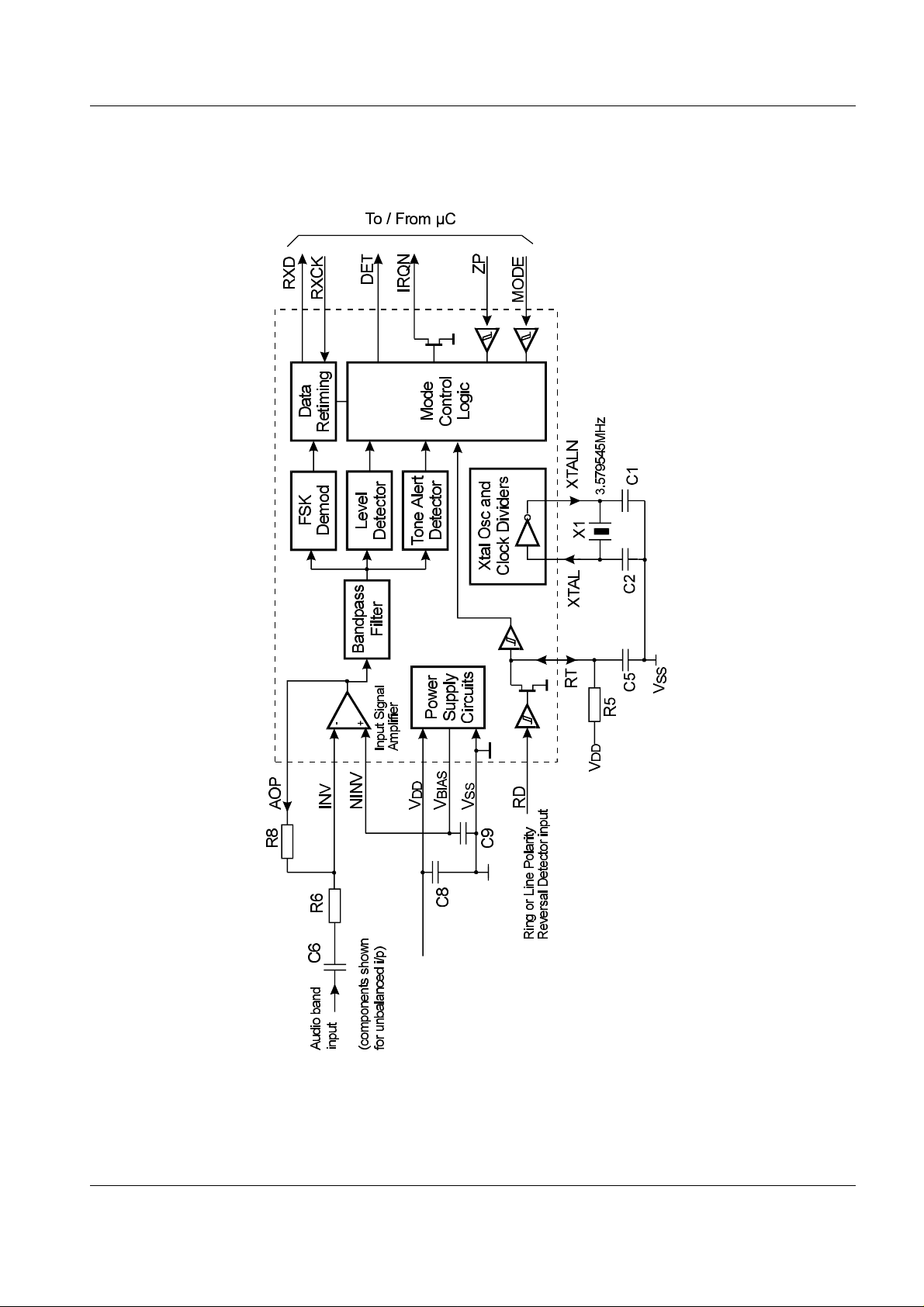
1.2 Block Diagram
Figure 1 Block Diagram
1996 Consumer Microcircuits Limited 3 D/602/5

Calling Line Identifier FX602
1.3 Signal List
Packages
D4 / P3
Signal Description
Pin No. Name Type
1 XTALN O/P The output of the on-chip Xtal oscillator inverter.
2 XTAL I/P The input to the on-chip Xtal oscillator inverter.
3 RD I/P (S) Input to the Ring or Line Polarity Reversal
Detector.
4 RT BI Open-drain output and Schmitt trigger input
forming part of the Ring or Line Polarity Reversal
detector. An external resistor to V
capacitor to V
should be connected to RT to
SS
DD
and a
filter and extend the RD input signal.
5 AOP BI The output of the on-chip Input Signal Amplifier
and the input to the Bandpass Filter.
6 INV I/P The inverting input to the on-chip Input Signal
Amplifier.
7 NINV I/P The non-inverting input to the on-chip Input
Signal Amplifier.
8 V
9 V
SS
BIAS
Power Negative supply rail (signal ground).
O/P Internally generated bias voltage, held at VDD/2
when the device is not in 'Zero-Power' mode.
Should be decoupled to V
by a capacitor
SS
mounted close to the device pins.
10 MODE I/P (S) Input used to select the operating mode. See
section 1.5.1.
11 ZP I/P (S) A high level on this input selects 'Zero-Power'
mode, a low level enables the Input Signal
Amplifier, the Bandpass Filter and either the FSK
or the Tone Alert circuits depending on the
MODE input.
1996 Consumer Microcircuits Limited 4 D/602/5

Calling Line Identifier FX602
Packages
D4 / P3
Signal Description
Pin No. Name Type
12 IRQN O/P An open-drain active low output that may be
used as an Interrupt Request / Wake-up input to
the associated µC. An external pull-up resistor
should be connected between this output and
.
V
DD
13 DET O/P A logic level output driven by the Ring or Line
Polarity Reversal Detector, the Tone Alert
Detector or the FSK Level detect circuits,
depending on the operating mode. See section
1.5.1.
14 RXCK I/P A logic level input which may be used to clock
received data bits out of the FSK Data Retiming
block.
15 RXD O/P A logic level output carrying either the raw output
of the FSK Demodulator or re-timed 8-bit
characters depending on the state of the RXCK
input. See section 1.5.6
16 V
DD
Notes: I/P = Input
I/P (S) = Schmitt trigger input
O/P = Output
BI = Bidirectional
Power The positive supply rail. Levels and thresholds
within the device are proportional to this voltage.
Should be decoupled to VSS by a capacitor
mounted close to the device pins.
1996 Consumer Microcircuits Limited 5 D/602/5
Calling Line Identifier FX602
µ
µ
µ
1.4 External Components
R1
470k
Ω
R2 See section 1.5.8 C1, C2 18pF
R3, R4, R5
R6, R7
R8
470k
470k
470k
680k
Ω
Ω
Ω for V
Ω for V
= 3.3V
DD
DD
= 5.0V
C3, C4
C5
C6, C7
C8,C9
0.1
0.33
680pF
0.1
(See section 1.5.2)
R9
240k
200k
Ω for V
Ω for V
= 3.3V
DD
= 5.0V
DD
(See section 1.5.2)
R10
R11
Ω
160k
Ω ±20%
100k
Resistors
±1%, capacitors ±20% unless otherwise stated.
X1 3.579545MHz
D1 - D4 1N4004
Figure 2 Recommended External Components for Typical Application
F
F
F
1996 Consumer Microcircuits Limited 6 D/602/5
Calling Line Identifier FX602
1.5 General Description
1.5.1 Mode Control Logic
The FX602's operating mode and the source of the DET and IRQN outputs are determined by the logic levels
applied to the MODE and ZP input pins;
ZP MODE Mode DET o/p from IRQN o/p from
0 0 Tone Alert Detect Tone Alert Signal
Detection
0 1 FSK Receive FSK Level Detector FSK Data Retiming
1 0 'Zero-Power' Ring or Line Polarity
Reversal Detector.
1 1 'Zero-Power' Ring or Line Polarity
Reversal Detector.
[1]
If enabled.
End of Tone Alert Signal.
Ring or Line Polarity
Reversal Detector.
[1]
.
Ring or Line Polarity
Reversal Detector.
Ring or Line Polarity
Reversal Detector.
-
In the 'Zero-Power' modes, power is removed from all of the internal circuitry except for the Ring or Line
Polarity Reversal Detector and the DET and IRQN outputs.
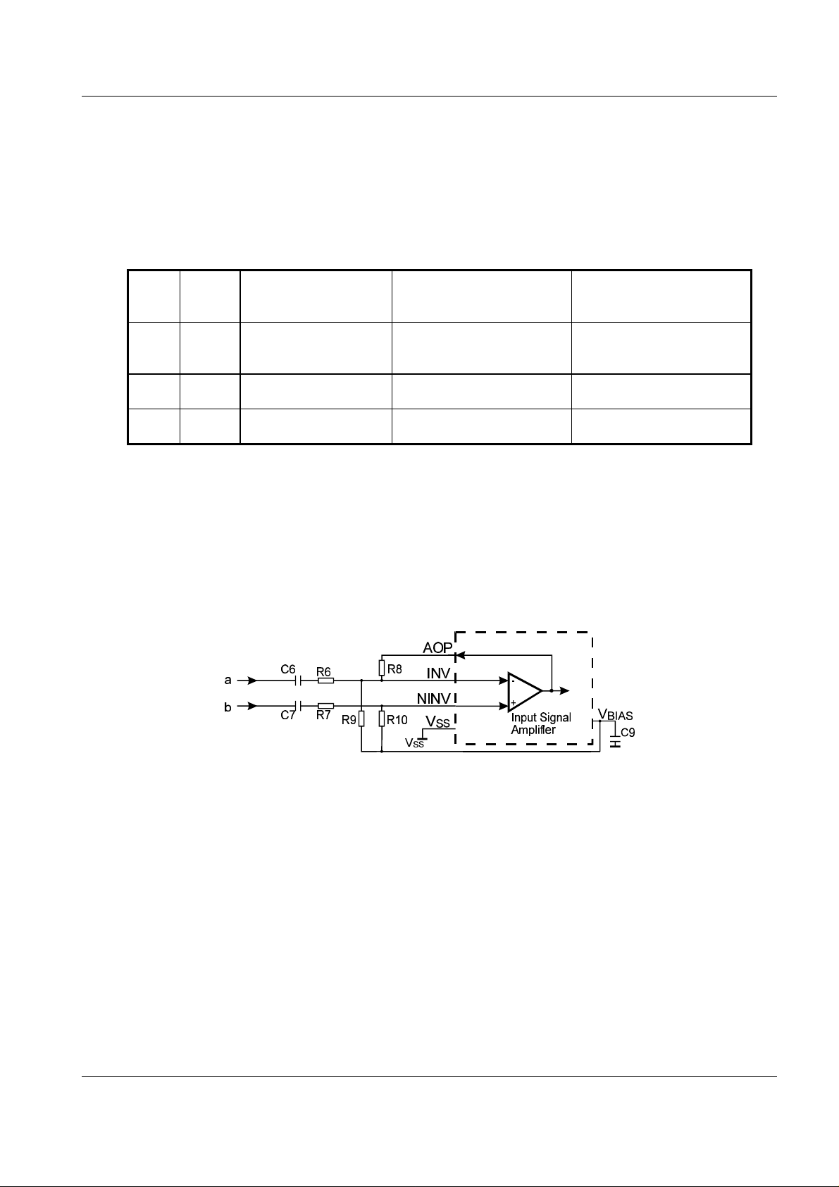
1.5.2 Input Signal Amplifier
This amplifier is used to convert the balanced FSK and Tone Alert signals received over the telephone line to
an unbalanced signal of the correct amplitude for the FSK receiver and Tone Alert Detector circuits.
Figure 3a : Input Signal Amplifier, balanced input configuration
The design equations for this circuit are;
Differential voltage gain V
R6 = R7 = 470k
Ω
/ V(b-a) = R8/R6
AOP
R10 = 160kΩ
R9 = R8 x R10 / (R8 - R10)
The target differential voltage gain depends on the expected signal levels between the A and B wires and the
FX602's internal threshold levels, which are proportional to the supply voltage.
The FX602 has been designed to meet the applicable specifications with R8 = 470k
rising to 680k
Ω at V
= 5.0V, and R9 should be 240kΩ at V
DD
= 3.3V and 200kΩ at V
DD
Ω at V
= 3.3V nominal,
DD
= 5.0V as shown in
DD
section 1.4 and Fig 3c.
1996 Consumer Microcircuits Limited 7 D/602/5
Calling Line Identifier FX602
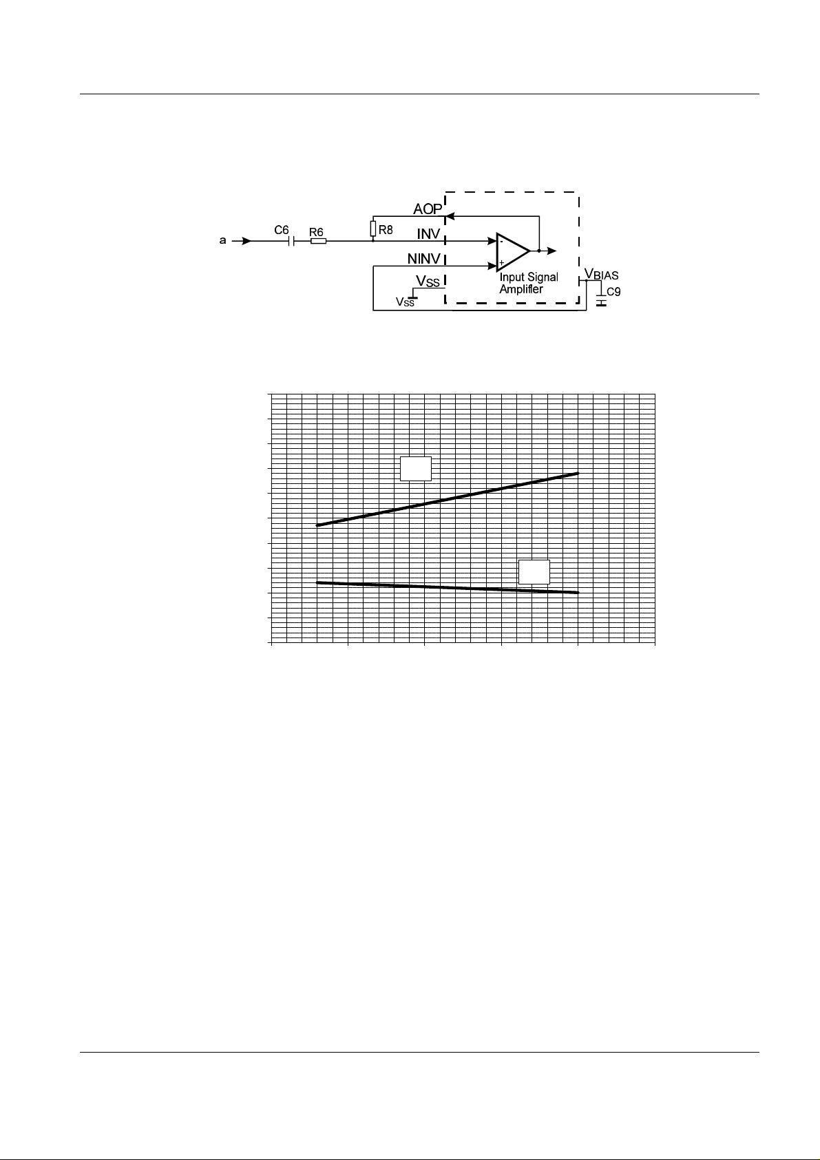
R8 and R9 : k ohms
The Input Signal Amplifier may also be used with an unbalanced signal source as shown in Figure 3b. The
values of R6 and R8 are as for the balanced input case.
Figure 3b : Input Signal Amplifier, unbalanced input configuration
1000
900
800
700
R8
600
500
400
300
R9
200
100
0
3 3.5 4 4.5 5 5.5
Nominal V
Figure 3c : Input Signal Amplifier, optimum values of R8 and R9 vs V
1.5.3 Bandpass Filter
Is used to attenuate out of band noise and interfering signals which might otherwise reach the FSK
Demodulator, Tone Alert Detector and Level Detector circuits. The characteristics of this filter differ in FSK and
Tone Alert modes. Most of the filtering is provided by Switched Capacitor stages clocked at 57.7kHz.
1.5.4 Level Detector
DD
DD
This block operates by measuring the level of the signal at the output of the Bandpass Filter, and comparing it
against a threshold which depends on whether FSK Receive or Tone Alert Detect mode has been selected.
In Tone Alert Detect mode the output of the Level Detector block provides an input to the Tone Alert Signal
Detector.
1996 Consumer Microcircuits Limited 8 D/602/5

Calling Line Identifier FX602
µ
µ
µ
µ
In FSK Receive mode the FX602 DET output will be set high when the level has exceeded the threshold for
sufficient time. Amplitude and time hysteresis are used to reduce chattering of the DET output in marginal
conditions.
Note that in FSK Receive mode this circuit may also respond to non-FSK signals such as speech.
See section 1.7.1 for definitions of Teon and Teoff
Figure 4 : FSK Level Detector operation
1.5.5 FSK Demodulator
This block converts the 1200 baud FSK input signal to a logic level received data signal which is output via the
RXD pin as long as the Data Retiming function is not enabled (see section 1.5.6). This output does not depend
on the state of the FSK Level Detector output.
Note that in the absence of a valid FSK signal, the demodulator may falsely interpret speech or other
extraneous signals as data.
1.5.6 FSK Data Retiming
The Data Retiming block extracts the 8 data bits of each character from the received asynchronous data
stream, and presents them to the
C under the control of strobe pulses applied to the RXCK input. The timing
of these pulses is not critical and they may easily be generated by a simple software loop. This facility removes
the need for a UART in the
C without incurring an excessive software overhead.
The block operates on a character by character basis by first looking for the mark to space transition which
signals the beginning of the start bit, then, using this as a timing reference, sampling the output of the FSK
Demodulator in the middle of each of the following 8 received data bits, storing the results in an internal 8-bit
shift register.
When the eighth data bit has been clocked into the internal shift register, the FX602 examines the RXCK input.
If this is low then the IRQN output will be pulled low and the first of the stored data bits put onto the RXD output
pin. On detecting that the IRQN output has gone low, the
C should pulse the RXCK pin high 8 times. The high
to low transition at the end of the first 7 of these pulses will be used by the FX602 to shift the next data bit from
the shift register onto the RXD output. At the end of the eighth pulse the FSK Demodulator output will be
reconnected to the RXD output pin. The IRQN output will be cleared the first time the RXCK input goes high.
Thus to use the Data Retiming function, the RXCK input should be kept low until the IRQN output goes low; if
the Data Retiming function is not required the RXCK input should be kept high.
The only restrictions on the timing of the RXCK waveform are those shown in Figure 5a and the need to
complete the transfer of all eight bits into the
C within 8.3mSec (the time of a complete character at 1200
baud).
1996 Consumer Microcircuits Limited 9 D/602/5
 Loading...