

Page 1

Xtreme/Multi-I/O
Users Guide
Connect Tech Inc.
42 Arrow Road
Guelph, ON CANADA
N1K 1S6
Tel: 519.836.1291
Toll Free: 800.426.8979 (North America Only)
Fax: 519.836.4878
Email: sales@connecttech.com
Web: www.connecttech.com
CTIM-00116 Revision: 0.02, Apr. 14, 2015
Page 2

Connect Tech - Xtreme/Multi-I/O - Users Guide
Document: CTIM-00116
Revision: 0.02 0.02
Page 2 of 50
Connect Tech Inc. Proprietary Information
Date: Apr. 14, 2015
Table of Contents
Table of Contents ................................................................................................................................ 2
Customer Support Overview ............................................................................................................. 4
Contact Information ............................................................................................................................ 4
Limited Lifetime Warranty .................................................................................................................. 5
Copyright Notice ................................................................................................................................. 5
Trademark Acknowledgment ............................................................................................................. 5
Revision History .................................................................................................................................. 6
Introduction ......................................................................................................................................... 7
Configuration....................................................................................................................................... 8
USB Configuration File Method .................................................................................................................. 8
USB Virtual COM Port Configuration Method ........................................................................................ 11
Serial Port Configuration Method ............................................................................................................. 13
Configuration Commands ................................................................................................................ 14
Memory vs IO Spaces ................................................................................................................................ 14
Memory Space ................................................................................................................................. 14
I/O Space .......................................................................................................................................... 14
Board Address Decoding Capabilities ................................ .......................................................... 14
Command Groups ...................................................................................................................................... 14
Serial Ports (UARTS) ................................................................................................................................. 15
Serial Ports Enable / Disable .................................................................................................................... 16
Serial Port Clocking ................................ ................................ ................................................................ .... 16
Serial Port DTR DSR Wrapback .......................................................................................................... 16
RS422/485 (Port-5) Settings ..................................................................................................................... 17
CAN Ports (SJA1000) ................................................................................................................................ 18
CAN Port Clocking ...................................................................................................................................... 19
Board Configuration ................................................................................................................................... 19
J1708 Configuration ................................................................................................................................... 19
Misc Configuration ................................................................................................................................ ...... 20
IO Address Ranges set with IOD command ................................................................................ 20
Testing / Debugging ................................................................................................................................... 20
Operation ........................................................................................................................................... 21
MultiTech Modules ..................................................................................................................................... 21
Serial Ports (Uarts) ..................................................................................................................................... 22
Uart Registers ................................................................................................................................... 22
RS232 Serial Ports .......................................................................................................................... 23
RS422/RS485 Serial & J1708 Port ............................................................................................... 24
CAN Ports (SJA1000) ................................................................................................................................ 25
CAN Port Registers ......................................................................................................................... 26
LED Header ................................................................................................................................................. 27
Board Control/Status Registers ................................................................................................................ 28
INTR_STAT Register (Offset 0x00, read-only) ............................................................................ 28
RESET_CONT Register (Offset 0x00, write-only) ...................................................................... 28
PC104 Bus Test .............................................................................................................................................................. 28
LED_CONT Register (Offset 0x01, read-write) ........................................................................... 29
J1708 Bus Interface .......................................................................................................................... 30
Page 3

Connect Tech - Xtreme/Multi-I/O - Users Guide
Document: CTIM-00116
Revision: 0.02 0.02
Page 3 of 50
Connect Tech Inc. Proprietary Information
Date: Apr. 14, 2015
Operation ..................................................................................................................................................... 30
Receiver ............................................................................................................................................ 30
Transmitter ........................................................................................................................................ 31
Detecting Transmission Errors or Potential Problems ............................................................................................... 31
Transmission Success ................................................................................................................................................... 31
J1708 Interrupts ............................................................................................................................... 32
Command, Control, Status Registers ...................................................................................................... 33
Command Register (Offset: 0x00) ................................................................................................. 33
Restart J1708 Bus SYNC .............................................................................................................................................. 33
Abort TX ........................................................................................................................................................................... 33
TX Kick ................................................................................................ ................................................................ ............. 33
Control Register (Offset: 0x01, Mem=0x04) ................................................................................ 34
Mask Reception of Good Transmitted Bytes .............................................................................................................. 34
TX Priority Register (Offset: 0x02) ................................................................................................................................ 34
TX Problem Limit Register (Offset: 0x03)..................................................................................... 34
J1708 Interrupt Status Register (Offset: 0x04) ............................................................................ 35
FIFO Status Register (Offset: 0x05) .............................................................................................. 35
RX EOM Level Register (Offset: 0x06) ......................................................................................... 36
RX Almost Full Level Register (Offset: 0x07) .............................................................................. 36
User-Ta Register (Offset: 0x08).................................................................................................... 37
Data FIFO’s ....................................................................................................................................... 37
J1708 IO ....................................................................................................................................................... 37
IO Connector & Jumper Locations ................................................................................................. 38
Serial Port-8 to Module GPIO Configuration .................................................................................. 39
Location of Resistors .................................................................................................................................. 39
FPGA Configuration Registers via SPI ........................................................................................... 40
Configuration Enhancements ................................................................................................................... 40
FPGA Configuration Registers ................................................................................................................. 41
PORT_CONFIG[N] (Reg 0 10) .................................................................................................. 43
IRQ_CONFIG[N] (Reg 12 16) ................................................................................................... 46
MEM_CONFIG (Reg 17)................................................................................................................. 47
MISC_CONFIG (Reg 18) ................................................................................................................ 49
FPGA_VERSION (Reg 19)............................................................................................................. 50
Page 4

Connect Tech - Xtreme/Multi-I/O - Users Guide
Document: CTIM-00116
Revision: 0.02 0.02
Page 4 of 50
Connect Tech Inc. Proprietary Information
Date: Apr. 14, 2015
Customer Support Overview
If you experience difficulties after reading the manual and/or using the product, contact the Connect Tech
Inc. reseller from which you purchased the product. In most cases the reseller can help you with product
installation and difficulties.
In the event that the reseller is unable to resolve your problem, our highly qualified support staff can
assist you. Our support section is available 24 hours a day, 7 days a week on our website at:
www.connecttech.com/sub/support/support.asp. See the contact information section below for more
information on how to contact us directly. Our technical support is always free.
Contact Information
Mail/Courier
Connect Tech Inc.
Technical Support
42 Arrow Road, Guelph, ON
Canada N1K 1S6
Email/Internet
sales@connecttech.com
support@connecttech.com
www.connecttech.com
Note:
Please go to the Download Zone or the Knowledge Database in the Support Center on the Connect Tech
Inc. website for product manuals, installation guides, device driver software and technical tips.
Submit your technical support questions to our customer support engineers via the Support Center on the
Connect Tech Inc. website.
Telephone/Facsimile
Technical Support Representatives are ready to answer your call Monday through Friday, from 8:30 a.m.
to 5:00 p.m. Eastern Standard Time. Our numbers for calls are:
Toll Free: 800-426-8979 (North America only)
Telephone: 519-836-1291 (Live assistance available 8:30 a.m. to 5:00 p.m. EST, Monday to Friday)
Facsimile: 519-836-4878 (online 24 hours)
Page 5

Connect Tech - Xtreme/Multi-I/O - Users Guide
Document: CTIM-00116
Revision: 0.02 0.02
Page 5 of 50
Connect Tech Inc. Proprietary Information
Date: Apr. 14, 2015
Limited Lifetime Warranty
Connect Tech Inc. provides a lifetime warranty for all of our products. Should this product, in Connect
Tech Inc.’s opinion, fail to be in good working order during the warranty period, Connect Tech Inc. will,
at our option, repair or replace this product at no charge, provided that the product has not been subjected
to abuse, misuse, accident, disaster or non Connect Tech Inc. authorized modification or repair.
You may obtain warranty service by delivering this product to an authorized Connect Tech Inc. business
partner or directly to Connect Tech Inc. along with proof of purchase. Product returned to Connect Tech
Inc. must be pre-authorized by Connect Tech Inc. with an RMA (Return Material Authorization) number
marked on the outside of the package and sent prepaid, insured and packaged for safe shipment. Connect
Tech Inc. will return this product by prepaid ground shipment service.
The Connect Tech Inc. lifetime warranty is defined as the serviceable life of the product. This is defined
as the period during which all components are available. Should the product prove to be irreparable,
Connect Tech Inc. reserves the right to substitute an equivalent product if available or to retract lifetime
warranty if no replacement is available.
The above warranty is the only warranty authorized by Connect Tech Inc. Under no circumstances will
Connect Tech Inc. be liable in any way for any damages, including any lost profits, lost savings or other
incidental or consequential damages arising out of the use of, or inability to use, such product.
Copyright Notice
The information contained in this document is subject to change without notice. Connect Tech Inc. shall
not be liable for errors contained herein or for incidental consequential damages in connection with the
furnishing, performance, or use of this material. This document contains proprietary information that is
protected by copyright. All rights are reserved. No part of this document may be photocopied,
reproduced, or translated to another language without the prior written consent of Connect Tech Inc.
Copyright 2013 by Connect Tech Inc.
Trademark Acknowledgment
Connect Tech Inc. acknowledges all trademarks, registered trademarks and/or copyrights referred to in
this document as the property of their respective owners.
Not listing all possible trademarks or copyright acknowledgments does not constitute a lack of
acknowledgment to the rightful owners of the trademarks and copyrights mentioned in this document.
Page 6

Connect Tech - Xtreme/Multi-I/O - Users Guide
Document: CTIM-00116
Revision: 0.02 0.02
Page 6 of 50
Connect Tech Inc. Proprietary Information
Date: Apr. 14, 2015
Revsion
Date
Changes
0.01
June 11, 2013
Original
0.02
Apr. 14, 2015
Add/revise information in the “Configuration” section, to clarify some important
points.
Revision History
Page 7

Connect Tech - Xtreme/Multi-I/O - Users Guide
Document: CTIM-00116
Revision: 0.02 0.02
Page 7 of 50
Connect Tech Inc. Proprietary Information
Date: Apr. 14, 2015
ESD Warning
Electronic components and circuits are sensitive to
ElectroStatic Discharge (ESD). When handling any circuit
board assemblies including Connect Tech COM Express
carrier assemblies, it is recommended that ESD safety
precautions be observed. ESD safe best practices include,
but are not limited to:
Leaving circuit boards in their antistatic packaging
until they are ready to be installed.
Using a grounded wrist strap when handling circuit
boards, at a minimum you should touch a grounded
metal object to dissipate any static charge that may
be present on you.
Only handling circuit boards in ESD safe areas,
which may include ESD floor and table mats, wrist
strap stations and ESD safe lab coats.
Avoiding handling circuit boards in carpeted areas.
Try to handle the board by the edges, avoiding
contact with components.
Introduction
Connect Tech’s Xtreme/Multi-I/O features dual SJA1000 CANbus controllers, isolated serial and CAN ports, and
two MultiTech Universal compatible sockets on a single PC/104 board design. This high density communication
board offers an all-in-one communication solution, optimizing Size, Weight, and Performance requirements. This
innovative product takes full advantage of the latest technologies in jumperless configuration, high voltage isolation
and advanced communication functionality.
Page 8

Connect Tech - Xtreme/Multi-I/O - Users Guide
Document: CTIM-00116
Revision: 0.02 0.02
Page 8 of 50
Connect Tech Inc. Proprietary Information
Date: Apr. 14, 2015
Configuration
This product can be configured for operation by 3 different modes.
1. In or Out of the target system, via a USB connection, using a configuration file.
2. In or Out of the target system, via a USB connection, using the Virtual COM port interface.
3. In the target system using an on-board serial port (which is usually accessed from the target system by
a Serial Port Driver software).
When the board is not installed in the target system, and then plugged into a USB port, a portion of the board’s
circuits are powered from the USB port which causes a (very small) USB Mass Storage Device and a Virtual
COM port interface to be available to the computer.
It is highly recommended that the USB port be used for configuring the board due to its simplicity.
USB Configuration File Method
When connected to a Windows computer the USB Plug&Play mechanism will automatically detect the
Xtreme/Multi-I/O as a small Mass Storage Device. This allows the board’s settings to be defined by a file
which is “placed” onto the storage device implemented on the product. The storage space is very limited
(about 8K bytes) and is only intended for the files related to the board’s setup.
The product is shipped with a default CONFIG.TXT file which has been placed there when the unit was tested.
This file is a good starting point for any customer desired settings.
Copy this file to some other folder on your computer system.
Edit the copy, and save it.
Delete the CONFIG.TXT file from the folder on the Xtreme/Multi-I/O board.
Copy the file back to the folder on the Xtreme/Multi-I/O board.
This file is processed (and the settings stored in non-volatile memory) as the file is streamed to the
board from the USB interface. The file cannot be edited directly on the device.
Remember, to change the configuration file, first delete it from the Xtreme/Multi-I/O board , then
copy a new file to the folder on the board.
If the board is “in” the target system (powered by the target system), then that system must be reset
(shutdown and powered back up) so that all the configuration changes will take effect.
If the board is “out of” the target system, then the settings are just retained for use when the board is
installed in the target system.
On power-up the on-board FPGA applies defaults for all configuration settings, and then, within 500
mS, the PIC32 applies all the settings that have been stored.
Three files are used
CONFIG.TXT
o Is the file that contains the configuration commands (see sample on install disk).
o This file is processed as soon as the file is “placed” onto the USB drive, with results placed
into the ERRORS.TXT file.
ERRORS.TXT
o A file that shows results of processing the CONFIG.TXT file (after it has been read and
processed).
README.TXT
o A short reminder file about how to perform the configuration.
Page 9

Connect Tech - Xtreme/Multi-I/O - Users Guide
Document: CTIM-00116
Revision: 0.02 0.02
Page 9 of 50
Connect Tech Inc. Proprietary Information
Date: Apr. 14, 2015
Page 10

Connect Tech - Xtreme/Multi-I/O - Users Guide
Document: CTIM-00116
Revision: 0.02 0.02
Page 10 of 50
Connect Tech Inc. Proprietary Information
Date: Apr. 14, 2015
Typical CONFIG.TXT file:
U1P=0x300
U2P=0x320
U1I=10
U2I=10
RS1=E
RS2=E
RS3=E
RS4=E
RS5=E
RS6=E
RS7=E
RS8=E
UPD
Resulting ERRRORS.TXT file:
U1P = (IO) 0x0300
U2P = (IO) 0x0320
U1I interrupt set to 10
U2I interrupt set to 10
Page 11

Connect Tech - Xtreme/Multi-I/O - Users Guide
Document: CTIM-00116
Revision: 0.02 0.02
Page 11 of 50
Connect Tech Inc. Proprietary Information
Date: Apr. 14, 2015
USB Virtual COM Port Configuration Method
When the Xtreme/Multi-I/O USB port is connected to a Windows computer and combined with the supplied
inf file it will create a virtual serial port that can be accessed using a serial terminal program like putty,
realterm, or equivalent, to configure the port settings interactively.
This method is great for doing experiments with the board’s setup for your application. The final setting
choices could then the committed to a CONFIG.TXT file so that the settings can be applied to other boards
using the Configuration File Method (described above).
NOTE: Port settings like baud rate, bits etc. do not matter when configuring the board via the virtual serial
port
Setup commands are entered by typing them on the terminal application’s used interface, or by using the file
sending (or transfer) facility of that application.
Each command is processed upon pressing “ENTER” key (CR character) and feedback is given in an “OK” or
“ERROR” with details format.
IMPORTANT: In order to have the settings committed to Non Volatile memory the “UPD” command must be
the last command executed. Certain settings will take effect as soon as the UPD command is executed, but
some settings (which affect the PC/104 IO or Memory address settings or interrupt settings) will not take effect
until the board is reset (or powered down then up again).
Page 12

Connect Tech - Xtreme/Multi-I/O - Users Guide
Document: CTIM-00116
Revision: 0.02 0.02
Page 12 of 50
Connect Tech Inc. Proprietary Information
Date: Apr. 14, 2015
Typical programming sequence:
CFG?
Xtreme/Multi-I/O Configuration
Firmware Version V1.00
FPGA Version A
Decode IO region is 10 bits
U1
U1P1 = (IO) 0x0300, 10
U1P2 = (IO) 0x0308, 10
U1P3 = (IO) 0x0310, 10
U1P4 = (IO) 0x0318, 10
U2
U2P1 = (IO) 0x0320, 10
U2P2 = (IO) 0x0328, 10
U2P3 = (IO) 0x0330, 10
U2P4 = (IO) 0x0338, 10
Uart Clock Setting = Mode 3 (1.8432MHz)
Uart 1 is ENABLED
Uart 2 is ENABLED
Uart 3 is ENABLED
Uart 4 is ENABLED
Uart 5 is ENABLED
Uart 6 is ENABLED
Uart 7 is ENABLED
Uart 8 is ENABLED
Port 5 termination enable/disable setting = T
Uart 1 DTR/DSR wrapback is CONNECTED
Uart 2 DTR/DSR wrapback is CONNECTED
Uart 3 DTR/DSR wrapback is CONNECTED
Uart 4 DTR/DSR wrapback is CONNECTED
Uart 5 DTR/DSR wrapback is CONNECTED
S1R?
Socket 1 RESET = NO
S2R?
Socket 2 RESET = NO
C1?
CAN1 = (IO) 0x0000, 255
CAN1 is DISABLED
C2?
CAN2 = (IO) 0x0000, 255
CAN2 is DISABLED
CM?
BASIC
Port 5 mode of operation set to J1708_MODE
Board base = (IO) 0x0ffe
CAN clock rate is currently set to 24MHz
J?
J1708 = (MEM) 0x00ff80, 255
Temperature is 301.65 K (28.50 C)
OK
DIS?
Invalid Command
RS8=D
OK
RS8?
Uart 8 is DISABLED
OK
SER?
SER
U1P1 = (IO) 0x0300, 10
U1P2 = (IO) 0x0308, 10
U1P3 = (IO) 0x0310, 10
U1P4 = (IO) 0x0318, 10
U2P1 = (IO) 0x0320, 10
U2P2 = (IO) 0x0328, 10
U2P3 = (IO) 0x0330, 10
U2P4 = (IO) 0x0338, 10
OK
UPD
OK
Page 13

Connect Tech - Xtreme/Multi-I/O - Users Guide
Document: CTIM-00116
Revision: 0.02 0.02
Page 13 of 50
Connect Tech Inc. Proprietary Information
Date: Apr. 14, 2015
Serial Port Configuration Method
When the Xtreme/Multi-I/O is installed into a computer and Serial Port 8 is enabled, a terminal program can be
used to access the settings of the board much like the Virtual Serial Port method using the OS running on the
PC/104 stack. Use a terminal program like qtalk, minicom, realterm, etc to configure the port settings
interactively.
This method is also applicable to situations where the application needs to change certain settings dynamically
as part of the application’s operation. However, the primary PC/104 Bus settings (like IO/Memory addresses or
interrupts) would not be candidates for any dynamic operations.
NOTE: Because this method requires some settings to already be enabled, we do not recommend this as a
primary way to configure the board, but rather suggest using the USB port.
Each command is processed upon pressing “ENTER” key (CR character) and feedback is given in an “OK” or
“ERROR” with details format.
Page 14

Connect Tech - Xtreme/Multi-I/O - Users Guide
Document: CTIM-00116
Revision: 0.02 0.02
Page 14 of 50
Connect Tech Inc. Proprietary Information
Date: Apr. 14, 2015
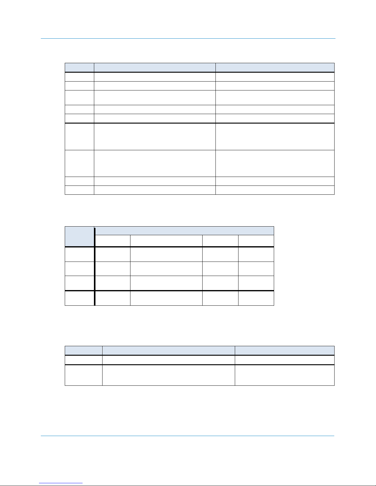
Group
Comment(s)
Serial Ports (UARTS)
Commands that set, or show, the Base Address (IO or Memory) or the IRQ assignments of
the UART Serial Ports.
Serial Ports Enable / Disable
Commands that allow individual serial ports to be Enabled or Disabled.
Serial Port Clocking
Commands that select, or show, a clock source for all Uart Serial Ports.
Serial Port DTR DSR
Wrapback
Commands that setup, or show the DTR to DSR wrapback on the chosen Port.
RS422/485 Port Settings
Commands that setup and show the RS422/485 Port settings.
CAN Ports (SJA1000)
Commands that set, or show, the Base Address (IO or Memory) or the IRQ assignments of
the CAN Ports.
CAN Ports Clocking
Commands that select, or show, a clock source for the CAN Ports.
Board Configuration
Commands to set, show the Base IO Address for the Board Control/Status Register.
J1708 Configuration
Commands to set, show the Base Address (IO or Memory) or the IRQ assignments of
J1708 Port.
Misc Configuration
Command to set, show a variety of miscellaneous settings.
Testing / Debugging
Commands that are used to test/debug the SPI interface between the PIC32 and FPGA.
Mainly used by software developers.
Configuration Commands
Memory vs IO Spaces
The first decision to make when configuring this board, is to determine whether the board will operate within
the Memory or I/O address Space of the computer system in which the board is installed. First, a quick
description of the two different Spaces.
Memory Space
Most (but not all) PC/104 CPU System board vendors provide one or more regions of Memory Addresses that
can be configured (or allocated) to the PC/104 Expansion bus connector(s) on CPU System board. This setup
may be performed via the BIOS setup or via jumpers or switches on the System board. This memory region is
usually located at addresses below the 1-Meg CPU memory address (commonly referred to as the Upper
Memory addresses), although some System boards allow the PC/104 Expansion Bus to be allocated to blocks of
addresses within the first 16-Meg of memory.
I/O Space
This region is supported by all PC/104 CPU System board vendors, and commonly consists of I/O Addresses
from 0x000 to 0x3FF, although some System boards support I/O addresses beyond 0x3FF, some even support
the full 16 bit IO range (0x0000 to 0xFFFF). (Note: Some I/O mapped PC/104 expansion boards only decode
the lowest 10 bits of the I/O address, therefore these boards restrict the usable I/O space to 0x3FF).
Board Address Decoding Capabilities
All the ports (Uart, CAN, J1708) of this board can be setup to reside in either IO or MEMORY space.
However, in most situations the Uart Serial Ports will be setup in IO space due to software limitations, and the
CAN Ports in MEMORY space because the SJA1000 devices have too many registers to fit easily in IO space.
The J1708 Port could be in either IO or MEMORY space as desired.
Command Groups
Page 15

Connect Tech - Xtreme/Multi-I/O - Users Guide
Document: CTIM-00116
Revision: 0.02 0.02
Page 15 of 50
Connect Tech Inc. Proprietary Information
Date: Apr. 14, 2015
Command
Operation
Notes
SER?
Query all the Address and IRQ settings for
both Uarts (1 and 2), (Ports 1 through 8)
Un?
Query the Address and IRQ settings for a Port group
n = 1 for Ports 1 through 4
n = 2 for Ports 5 through 8
UnP?
Query the Address setting for a Port group
n = (as above)
UnPx?
Query the Address setting for a specific Port.
n = (as above)
x = 1,2,3,4 for a specific Port
UnI?
Query the IRQ setting for a Port group
n = (as above)
UnIx?
Query the IRQ setting for a specific Port
n and x = (as above)
UnP=v
Set the Address for a group of Ports.
See Note [1] below.
n = (as above)
v= Base Address value can be from:
See the IOD command for setting the IO decoding
width, and the resulting IO address range.
UnI=v
Set the IRQ for a group of Ports.
n = (as above)
v= one of these possible IRQ selections:
3,4,5,6,7,9,10,11,12,14,15
Serial Ports (UARTS)
These commands allow the 8 Uart Serial Ports to be configured with Address and IRQ assignments. The
assignments can also be queried.
Notes:
1. When the Address is entered as a single value (ie: U1P=0x300), then this is the Base Address for the group of Ports,
with each successive Port being set 0x08 bytes beyond the previous Port. (for this example: 0x300, 0x308, 0x310,
0x318). However, when the Addresses are entered as a comma separated list (ie: U2P=0x200,0x250,0x300,0x410),
then each Port is set to the Address value indicated.
2. Each enabled Port must have a unique Address which is at least 8 bytes away from any other Port’s Address.
3. All Uart Serial Ports can be set to the same IRQ number.
4. Ports are assumed to be IO Space if the address is entered as 3 or 4 HEX digits (ie: 0x300), otherwise Memory Space
if the address is longer (ie: 0xD0000).
5. The “0x” preceding an address value signifies HEX, otherwise decimal is assumed.
Page 16

Connect Tech - Xtreme/Multi-I/O - Users Guide
Document: CTIM-00116
Revision: 0.02 0.02
Page 16 of 50
Connect Tech Inc. Proprietary Information
Date: Apr. 14, 2015
Command
Operation
Notes
RSn?
Query the Enable / Disable state of a Port.
n = 1 through 8
RSn=v
Set the Enable / Disable state of a Port.
n = (as above)
v = ‘E’ to enable the Port
‘D’ to disable the Port
‘C’ to connect port to PIC32 CPU (Port 8 only)
‘S’ to connect port to Module Socket-2 (Port 8 only)
note [2] below.
Command
Operation
Notes
UCD?
Query the Uart clock setting
UCD=v
Set the Uart clock setting
v = 0 (or ‘F’) for 14.7456 MHz
1 for 7.3728 MHz
2 for 3.6864 MHz
3 (or ‘S’) for 1.8432 MHz
Command
Operation
Notes
DSRn?
Query the DTR to DSR wrapback.
n = 1 through 5, Port number
DSRn=v
Set the DTR to DSR wrapback.
n = (as above)
v = ‘C’ = connected (enabled)
‘D’ = disconnected (disabled)
Serial Ports Enable / Disable
These commands allow the 8 Uart Serial Ports to be enabled or disabled. The assignments can also be queried.
When a port is disabled…
The respective Isolated Line Transceiver is turned-off, to reduce power consumption.
The decoding of the IO or Memory space is disabled.
The Port’s interrupt signal is disconnected (disabled) from asserting the IRQ.
Notes:
1. The LED Outputs obtain their isolated power from the Port-4 Isolated Line Transceiver, therefore
Port-4 must be Enabled to allow the LED outputs to operate properly.
2. The connections between Serial Port-8 and the GPIO pins of Module Socket-2 are implemented with
zero ohm resistors to select which GPIO pins to use (see the “Serial Port-8 to Module GPIO
Configuration”section for details).
Serial Port Clocking
These commands allow 4 different clock choices for the Uart Serial Ports. Both Uart (all serial ports) are
clocked from the same source.
Serial Port DTR DSR Wrapback
These commands allow the DTR signal to be wrapped back (connected) to the DSR signal for the first 5 Uart
Serial Ports. When the wrapback is disable, the DSR signal is held at the inactive state.
Page 17

Connect Tech - Xtreme/Multi-I/O - Users Guide
Document: CTIM-00116
Revision: 0.02 0.02
Page 17 of 50
Connect Tech Inc. Proprietary Information
Date: Apr. 14, 2015
Command
Operation
Notes
P5?
Query the Port-5 mode of operation
RSZ?
Query the Termination state of Port-5
P5=v
Set the Port-5 mode of operation
v = ‘F’ for Full Duplex
‘H’ for ½ Duplex
‘J’ for J1708 mode
RSZ=v
Set the Termination state of Port-5
v = ‘T’ to enable the Termination
‘O’ to disable the Termination
See note [1] below.
RS422/485 (Port-5) Settings
Page 18

Connect Tech - Xtreme/Multi-I/O - Users Guide
Document: CTIM-00116
Revision: 0.02 0.02
Page 18 of 50
Connect Tech Inc. Proprietary Information
Date: Apr. 14, 2015
Command
Operation
Notes
CAN?
Query all the Address and IRQ settings for
both CAN (1 and 2) Ports
Cn?
Query the Address and IRQ settings for a CAN Port
n = 1 for CAN1
n = 2 for CAN2
CnP?
Query the Address setting for a CAN Port
n = (as above)
CI?
Query the IRQ setting for both CAN Ports
CnI?
Query the IRQ setting for a CAN Port
n = (as above)
CD?
Query the CAN Port IO or MEMORY region setting
CM?
Query the CAN decoding mode as BASIC or PELICAN
CSn?
Query the Enable or Disable state of a CAN Ports
n = 1 for CAN1
n = 2 for CAN2
CP=v
Set the Address for a CAN Port
See Note [1] below.
v= Base Address value
See Note [3] below.
CI=v
Set the IRQ for both CAN Ports.
See Note [2] below.
v= IRQ selections:
3,4,5,6,7,9,10,11,12,14,15
CnI=v
Set the IRQ for a specific CAN Port.
n = (as above)
v= IRQ selections:
3,4,5,6,7,9,10,11,12,14,15
CD=v
Set the CAN Port decoding region.
v = ‘P’ for IO region decoded
‘M’ for MEMORY region decoded
CM=v
Set the CAN Port Address decoding mode.
v = ‘B’ for “BASIC” mode (0x20 boundary)
‘P’ for “PeliCAN” mode (0x80 boundary)
See Note [4] below.
CSn=v
Set the Enable / Disable state of a CAN Port
v = ‘E’ to enable the Port
‘D’ to disable the Port
CAN Ports (SJA1000)
These commands allow the 2 CAN Ports to be configured with Address and IRQ assignments. The
assignments can also be queried.
Notes:
1. When the Address is entered as a single value (ie: CP=0x400), then this is the Base Address for the group of Ports,
with the next Port being set Base+0x80 bytes. However, when the Addresses are entered as a comma separated list (ie:
CP=0x400,0x500), then each Port is set to the Address value indicated.
Examples:
o With CM=B, CP=0x400
CAN Port-1 = 0x400, CAN Port-2 = 0x480 (decoding width = 0x20)
o With CM=P, CP=0x400
CAN Port-1 = 0x400, CAN Port-2 = 0x480 (decoding width = 0x80)
o With CP=0x0C0000 (the CM setting is ignored)
CAN Port-1 = 0x0C0000, CAN Port-2 = 0x0C0080 (decoding width = 0x80)
o With CP=0x0C0000,0x0C2000 (the CM setting is ignored)
CAN Port-1 = 0x0C0000, CAN Port-2 = 0x0C2000 (decoding width = 0x80)
2. When the IRQ is entered as a single value (ie: CI=5), then this IRQ number is applied to both CAN Ports. However,
when the IRQs are entered as a comma separated list (ie: CI=9,11) then each CAN Port is set to the IRQ value
indicated.
3. The value specified for the CP= command implies either IO or Memory Space. When the value for the CP command
is a 3 digit IO address in Hex (0x000 to 0xFE0 or 0xF80), the IO Space is implied. When the value for the CP
command is a 6 digit Hex value (0x000000 to 0xFFFFE0 or 0xFFFF80).
decoding width, and the resulting IO address range.
See the IOD command for setting the IO
4. The address decoding mode is used only when the CAN Ports are mapped into and IO region (with CD=P). The
SJA1000 must be set to operate in the mode that matches this address decoding mode (see the CLOCK DIVIDER
REGISTER in the SJA1000 data sheet for details).
Page 19

Connect Tech - Xtreme/Multi-I/O - Users Guide
Document: CTIM-00116
Revision: 0.02 0.02
Page 19 of 50
Connect Tech Inc. Proprietary Information
Date: Apr. 14, 2015
Command
Operation
Notes
CC?
Query the CAN clocking selection.
CC=v
Set the CAN clock selection.
v = 16 or 24 (value indicates the frequency in MHz)
Command
Operation
Notes
BP?
Query the Board Base IO Address setting.
BP=v
Set the Board Base IO Address setting.
v= Base Address value can be from:
See the IOD command for setting the IO decoding
width, and the resulting IO address range.
Command
Operation
Notes
J?
Query the J1708 Base Address and IRQ settings
JP?
Query the J1708 Base Address setting
JI?
Query the J1708 IRQ setting
JS?
Query the Enable / Disable state of the J1708 Port.
JP=v
Set the J1708 Port Base Address.
v= Base Address value
See Note [1] below.
See the IOD command for setting the IO decoding
width, and the resulting IO address range.
JI=v
Set the J1708 Port IRQ.
v= IRQ selections:
3,4,5,6,7,9,10,11,12,14,15
JS=v
Set the Enable / Disable state of the J1708 Port.
v = ‘E’ to enable the Port
‘D’ to disable the Port
See note [2] below
CAN Port Clocking
The CAN controller (SJA1000) can be clocked by 2 different frequencies.
Board Configuration
This product contains a group of registers that are used at “run-time” to perform a variety of functions. This
Command sets or shows the Base IO Address setting for these registers.
J1708 Configuration
On this product the J1708 controller is implemented within the FPGA and is separate from the Uart Serial
Ports. These commands allow the J1708 Port to be configured with Address and IRQ assignments. The
assignments can also be queried.
Notes:
1. The value specified for the JP= command varies depending on whether the IO or MEMORY region is desired for the
J1708 Port. When IO region is desired, the value for the JP= command is a 3 digit IO address in Hex (000 to FE0 or
F80). When MEMORY region is desired, the value is a 6 digit Hex value (000000 to FFFFE0 or FFFF80).
2. When the J1708 Port is disabled…
The decoding of the IO or Memory space is disabled.
The Port’s interrupt signal is disconnected (disabled) from asserting the IRQ.
Page 20
Connect Tech - Xtreme/Multi-I/O - Users Guide
Document: CTIM-00116
Revision: 0.02 0.02
Page 20 of 50
Connect Tech Inc. Proprietary Information
Date: Apr. 14, 2015
Command
Operation
Notes
TRD?
Query the board temperature.
Value return is degrees Kelvin
CFG?
Query all configuration settings.
VER?
Query the PIC32 and FPGA firmware version.
PIC32 firmware version appears as “Vx.y”
FPGA version appears as a letter “A”, “B”, “C”, etc.
IOD?
Query the IO Address decoding range (or width).
SnR?
Query the reset state of the Module Sockets
IOD=v
Set the IO Address decoding width.
v = 10, 11 or 12
=10 performs “10-bit” IO decoding.
=11 performs “11-bit” IO decoding.
=12 performs “12-bit” IO decoding.
SnR=v
Set the reset state of the Module Sockets
v = ‘Y’ to Assert the reset
‘N’ to De-assert reset
n = 1 = Apply to Socket #1
2 = Apply to Socket #2
UPD
Write configuration changes to Non-Volatile storage
IO
Decode
Width
Base IO Address Range
Uart Ports
CAN Ports
J1708 Port
Board
10
0x000 to
0x3F8
0x000 to 0x3E0 (Basic mode)
0x000 to 0x380 (Pelican mode)
0x000 to
0x3E0
0x000 to
0x3FE
11
0x000 to
0x7F8
0x000 to 0x7E0 (Basic mode)
0x000 to 0x780 (Pelican mode)
0x000 to
0x7E0
0x000 to
0x7FE
12
0x000 to
0xFF8
0x000 to 0xFE0 (Basic mode)
0x000 to 0xF80 (Pelican mode)
0x000 to
0xFE0
0x000 to
0xFFE
Address
Boundaries
0x08
0x20 (Basic mode)
0x80 (Pelican mode)
0x20
0x02
Command
Operation
Notes
SPIR reg
Perform an SPI read operation from the indicated register.
reg is a decimal number 0 to N
SPIW reg value
Perform an SPI write operation to the indicated register.
reg is a decimal number 0 to N
value is a 16 bit HEX number as appropriate
for the register.
Misc Configuration
IO Address Ranges set with IOD command
The IO Address range depends on the IO Address decoding width.
Testing / Debugging
A couple of commands are available that directly write or read the FPGA registers that are accessed via an SPI
port between the PIC32 and the FPGA.
Page 21

Connect Tech - Xtreme/Multi-I/O - Users Guide
Document: CTIM-00116
Revision: 0.02 0.02
Page 21 of 50
Connect Tech Inc. Proprietary Information
Date: Apr. 14, 2015
Operation
MultiTech Modules
Two Multitech wireless modules can be plugged into the top side of this board. Each communicates through a
serial port as described in the next section.
Refer to the “IO Connector & Jumper Locations”section for the locations of the Sockets.
Each module can be powered by either 5V or 3.3V by installing jumpers in the appropriate locations. Jumpers
are installed in pairs as shown below…
PCB Locations
Page 22

Connect Tech - Xtreme/Multi-I/O - Users Guide
Document: CTIM-00116
Revision: 0.02 0.02
Page 22 of 50
Connect Tech Inc. Proprietary Information
Date: Apr. 14, 2015
Serial Ports (Uarts)
These serial ports are implemented with two, “554” style (quad) Uart devices, for a total of 8 serial ports.
These are used for various purposes on the board.
First Quad Uart
o Four isolated RS232 interface
o Port Order
1 = Header P1
2 = Header P2
3 = Header P3
4 = Header P4
Second Quad Uart
o One isolated RS422/RS485 Port
o Two ports connected to Module sockets P6 and P7
o One port connected to PIC32 (for Command line based configuration changes)
o Port Order
1 = RS422/RS485 to Header P5
2 = MultiTech module P6
3 = MultiTech module P7
4 = To PIC32
Uart Registers
Refer to the Exar ST16C554 data sheet for details of the Uart registers. A brief screenshot is shown here for
convenience.
Page 23

Connect Tech - Xtreme/Multi-I/O - Users Guide
Document: CTIM-00116
Revision: 0.02 0.02
Page 23 of 50
Connect Tech Inc. Proprietary Information
Date: Apr. 14, 2015
Pin
Number
Signal
1
N/C 2 N/C
3
RxD
4
RTS 5 TxD
6
CTS
7
N/C 8 N/C
9
GND (Isolated)
10
+5V (Isolated), limited to 100 mA
RS232 Serial Ports
These 4 serial ports connect to Header group P1to P4 as indicated in the sketch below, as viewed from the edge
of the board. Each port can support bit rates up to 921.6K, and has xxxx V
from the main circuits.
[1]
of isolation, from each other and
N/C = Not Connected
Page 24

Connect Tech - Xtreme/Multi-I/O - Users Guide
Document: CTIM-00116
Revision: 0.02 0.02
Page 24 of 50
Connect Tech Inc. Proprietary Information
Date: Apr. 14, 2015
Pin
Number
Signal
1
J1708+
2
J1708-
3
RX+ 4 TX+
5
TX-
6
RX-
7
Slow Slew Rate enable (strap to pin-9)
8
Termination Enable (strap to pin-10)
9
GND (Isolated)
10
+5V (Isolated), limited to 100 mA
RS422/RS485 Serial & J1708 Port
This serial port connects to Header P5 as indicated in the sketch below, as viewed from the edge of the board.
Each port can support bit rates up to 921.6K, and has xxxx V
[1]
of isolation, from each other and from the main
circuits.
When the J1708 Port is enabled (by the JS= command), this isolated interface circuit is re-commissioned for
the J1708 port. The IO header has special connection pins for the J1708 Port. Pins 3-4 and 5-6 must be
shorted so that the J1708 interface will operate properly.
Note: On the Rev.C version of the board, the Pins 3-4 and 5-6 connections are not required, instead a jumper
(J5) is provided to perform the signal shorting. Install 2, 50 mil jumpers on J5 as shown here…
Page 25

Connect Tech - Xtreme/Multi-I/O - Users Guide
Document: CTIM-00116
Revision: 0.02 0.02
Page 25 of 50
Connect Tech Inc. Proprietary Information
Date: Apr. 14, 2015
Pin
Number
Signal
1
N/C
2
GND (Isolated)
3
CAN-
4
CAN+
5
GND (Isolated)
6
CAN+ (for termination strap)
7
CAN Bus Termination Resistor
(strap to pin-6)
8
+5V (Isolated), limited to 5 mA
9
N/C
10
N/C
CAN Ports (SJA1000)
These CAN Ports are implemented with industry standard SJA1000 devices. The CAN Bus interface circuits
are isolated from the other circuits on the board, and are connected to IO headers P9 and P10.
Each port can support bit rates up to 1M, and has xxxx V
circuits.
Both CAN controllers are clocked from the same source, which can be setup to be either 16 MHz or 24 MHz.
[1]
of isolation, from each other and from the main
Page 26

Connect Tech - Xtreme/Multi-I/O - Users Guide
Document: CTIM-00116
Revision: 0.02 0.02
Page 26 of 50
Connect Tech Inc. Proprietary Information
Date: Apr. 14, 2015
CAN Port Registers
Refer to the NXP SJA1000 data sheet for details of the CAN Controller registers. A brief screenshot is shown
here for convenience.
Page 27

Connect Tech - Xtreme/Multi-I/O - Users Guide
Document: CTIM-00116
Revision: 0.02 0.02
Page 27 of 50
Connect Tech Inc. Proprietary Information
Date: Apr. 14, 2015
Pin
Number
Signal
Primary Function
Secondary Function
1
LED1-
Link-Activity from Module-1 (P6)
Software driven, from register in FPGA
2
LED1+
3
LED2+
Link-Activity from Module-2 (P7)
Software driven, from register in FPGA
4
LED2-
5
LED3+
From GPIO (pin-51) Module-2 (P7)
Software driven, from register in FPGA
6
LED3-
7
LED4+
Uart ports operating at highest
clock rate (14.7456 MHz)
Software driven, from register in FPGA
8
LED4-
9
LED5+
Software driven, from PIC32
Software driven, from PIC32
10
LED5-
LED Header
Five LED’s can be connected to the P11 header. The LED drive circuit is isolated from the other circuits on the
board, and gets its power from the P4 serial port isolator (U24). Port-4 must be enabled (see the “Serial Ports
Enable / Disable” section for details) so that power is available for the LED outputs.
Each LED is current limited on the board to approximately 6.5 mA.
Notes:
1. The software driven function of LED’s 1 through 4, is described in the “LED_CONT Register (Offset
0x01, read-write)” section.
Page 28

Connect Tech - Xtreme/Multi-I/O - Users Guide
Document: CTIM-00116
Revision: 0.02 0.02
Page 28 of 50
Connect Tech Inc. Proprietary Information
Date: Apr. 14, 2015
Register
Function
IO Offset
INTR_STAT
Interrupt Status
0x00 (read-only)
RESET_CONT
Reset Control
0x00 (write-only)
LED_CONT
LED Control
0x01 (write-read)
Control Item
Bit
Offset
Bit
Value
Comment(s)
Uart Group-1
0
0x1
Uart Ports 1 through 4 interrupt is active
Uart Group-2
1
0x2
Uart Ports 5 through 8 interrupt is active
CAN Port-1
2
0x4
CAN Port 1 interrupt is active
CAN Port-2
3
0x8
CAN Port 2 interrupt is active
J1708 Port
4
0x10
J1708 Port interrupt is active
Unused
5 7
Reserved for future use
Control Item
Bit
Offset
Bit
Value
Comment(s)
PIC32_RST
0
0x1
PIC32 Microcontroller Reset
Uart Group-1_RST
1
0x2
Uart Ports 1 through 4 reset
Uart Group-2_RST
2
0x4
Uart Ports 5 through 8 reset
CAN Port-1_RST
3
0x8
CAN Port 1 reset
CAN Port-1_RST
4
0x10
CAN Port 2 reset
Module-1_RST
5
0x20
MultiTech Module-1 reset
Module-2_RST
6
0x40
MultiTech Module-2 reset
BUS_TEST
7
0x80
PC104 Address Bus test mode enable
Board Control/Status Registers
Implemented in the FPGA is 2 registers which assist with the operation of the board. The Base PC/104
IO-Address for these registers is defined by the BP= command.
INTR_STAT Register (Offset 0x00, read-only)
Software can use the Interrupt Status register to determine which interrupts are active. All bits are
“active-high”.
RESET_CONT Register (Offset 0x00, write-only)
Software can use the Miscellaneous Control register to reset various circuits on the board. Writing a “1” to the
respective bit, will hold the reset on the respective circuit.
PC104 Bus Test
This bit enables a mode where the PC104 Address Bus signals can be confirmed as functioning. This bit
should be set to zero for normal operation of the board.
Page 29

Connect Tech - Xtreme/Multi-I/O - Users Guide
Document: CTIM-00116
Revision: 0.02 0.02
Page 29 of 50
Connect Tech Inc. Proprietary Information
Date: Apr. 14, 2015
Control Item
Bit
Offset
Bit
Value
Comment(s)
LED1_STATE
0
0x1
=0, LED Off (after approximately 75 mS)
=1, LED On immediately
See Note [2] below
LED1_ENAB
1
0x2
=0, Primary LED function is active
=1, LED operation controlled by the LEDn_STATE bit.
See Note [1] below
LED2_STATE
2
0x4
Same as above for LED2
LED2_ENAB
3
0x8
Same as above for LED2
LED3_STATE
4
0x10
Same as above for LED3
LED3_ENAB
5
0x20
Same as above for LED3
LED4_STATE
6
0x40
Same as above for LED4
LED4_ENAB
7
0x80
Same as above for LED4
LED_CONT Register (Offset 0x01, read-write)
This register provides the secondary LED functions for the LED header (P11).
Notes:
1. The ENAB bit(s) allows software to take control the LED outputs (1 to 4). The primary function of the
LED is inhibited when the ENAB bit is On.
2. The LED output remains ON for as long as the STATE bit in ON (=1). When the STATE bit is turned
OFF, a timer in the FPGA hardware holds the LED output ON for 50 to 100 mS. This allows software to
“blink” an LED without needing to perform any timing.
Page 30

Connect Tech - Xtreme/Multi-I/O - Users Guide
Document: CTIM-00116
Revision: 0.02 0.02
Page 30 of 50
Connect Tech Inc. Proprietary Information
Date: Apr. 14, 2015
Control Item
Address Offset
Command, Control, Status Registers
0x00 0x0F
Data FIFO’s
0x10 0x1F
J1708 Bus Interface
Operation
The J1708 specification goes to significant detail about the requirements of the J1708 Bus interface, this
section elaborates on the specifics of this implementation of that interface. The J1708 specification should be
consulted to get a general sense of the nature of this communications protocol before continuing with the
description below.
The J1708 controller is implemented entirely in the FPGA. It consists of three (3) tightly coupled control
blocks; the Transmitter, Receiver and Interrupt Generator. The Transmitter and Receiver blocks share a
common Data Bit PLL clocking mechanism which clocks data bits at 9600 bps.
By its nature, the J1708 Bus is a ½ Duplex Bus, which causes any transmitted bits to also be received. It is this
behaviour that allows transmitted bytes to be checked for collisions with other bits being transmitted by other
device(s) on the J1708 Bus.
Receiver
The Receiver consists of a PLL clock recovery block, a control state machine, data bit shifting block and
controlling registers. The clock recovery block finds falling edges within the receive data stream and uses them
the align the phase of the data clock, in order to properly receive the data bits. This clock is also used by the
Transmitter.
Upon power up (or when the Restart J1708 Bus SYNC command is issued) the Receiver will begin hunting for
19 consecutive Bus Idle periods. During this time both the Receiver and Transmitter will not receive/send any
data bits. Once 19 Idles are found the Receiver and Transmitter become operational.
Data bytes are framed in the usual asynchronous fashion, ie: 1-START bit, 8 data bits, 1-STOP bit.
When a legal START bit is detected, the following data bits are shifted into the Receiver data shift register
(only 8 bits are collected). The following bit is considered to be the STOP bit, and if it is legal (=1) the data
byte is placed into the FIFO.
Note: Because the J1708 Bus is ½ duplex, any transmitted bits are also received. This implementation
can either store the transmitted bytes into the Receiver FIFO, or can mask (prevent) them from being
stored. This feature is controlled by the Mask Reception of Good Transmitted Bytes control bit. Refer to
the Control Register section below for more details. Even with this feature enabled, the Receiver
always receives the transmitted bits, so that error conditions in the Transmitter can be detected.
Messages are groups of one or more data bytes that can be considered to belong together. Since there are no
delineating features in the data bytes themselves, the only feasible way to delineate (separate) received
messages is by determining when the J1708 Bus has gone Idle for a certain amount of time. The RX EOM Level
register allows the host software to be notified when the desired Bus Idle interval has been reached (via and
interrupt), so that data can be retrieved from the Receiver FIFO.
Various Receiver conditions cause an interrupt to be generated. The situations/conditions that generate
interrupts are covered in more detail later in the J1708 Interrupts section, but are listed here for reference…
Receiver EOM (End of Message)
Page 31

Connect Tech - Xtreme/Multi-I/O - Users Guide
Document: CTIM-00116
Revision: 0.02 0.02
Page 31 of 50
Connect Tech Inc. Proprietary Information
Date: Apr. 14, 2015
Receiver FIFO Almost Full
Receiver FIFO Full
Transmitter
The Transmitter consists of a control state machine block, data bit shifting block, and controlling registers. It is
clocked by the Data Clock that is recovered by the Receiver. In this way the starting of a transmitted message
can be accurately timed from the end of the last message “seen” on the J1708 Bus. This accurate timing is the
essence of J1708 Bus messaging.
Transmission starts as soon as data byte(s) are written to the Transmitter FIFO, however the actual bit
transmission is delayed until after the J1708 Bus has been Idle for a certain amount of time. This time is
measured in Bit intervals from the end of the last message “seen” on the J1708 Bus. The duration of the delay
is controlled by the TX Priority register setting, and by a collision and re-transmission algorithm (which delays a
random number of Bus Idle periods). In special circumstances a user controlled delay can be setup (with the
User-Ta register setting).
Software Implementation Note:
An alternate method to “kick off” Transmitter activity, is by using the TX Kick command, which causes the
TX FIFO Empty interrupt to occur. In response to this interrupt, software can load data into the TX FIFO,
which causes the transmission to begin.
Transmission continues until one of 3 situations occur.
The Transmitter FIFO becomes empty.
An error is detected in the data bytes sent.
The software issues an Abort TX command.
Detecting Transmission Errors or Potential Problems
Since multiple devices can begin their bit transmissions at the same (or nearly same) point in time, there is a
variety of transmission issues that are detected and acted upon by the this J1708 controller. The detection is
possible because all transmitted bits are also received. At each byte boundary the byte sent is compared to the
byte received.
1. In circumstances where there is heavy data traffic on the Bus, there may be situations where the
transmission of a message cannot begin because there is never a sufficiently long enough Idle period
on the bus. Each time a transmission is refused (preempted) by another transmission on the bus, this
condition is counted in a “TX Problem” counter. Also, if a collision occurs while the first byte of the
message is being transmitted, then again, this problem counter is incremented. This problem counter
value is compared against the TX Problem Limit register value. If the limit is reached an interrupt is
generated to the software. With the collision scenario, the Transmitter will again delay for the
required amount of Idle periods and attempt to re-send the message. This process repeats (forever)
until the transmission start is successful or software takes some action (in response to the problem
interrupt).
2. In rare circumstances there may be a collision on the Bus after the first byte is successfully sent. In
this case the Transmitter self aborts as soon as the current byte is finished, the Transmitter FIFO is
flushed (emptied) and the TX Abort interrupt occurs.
This TX Problem counter is reset (to zero) when the first byte of a new/next message (packet) is
loaded from the FIFO into the TX data shift register.
Transmission Success
In the absence of any errors or commanded aborts, the Transmitter will continue sending data bytes until the
data FIFO is empty. When the last bit of the last byte is sent, this is the moment in time where the transmission
Page 32

Connect Tech - Xtreme/Multi-I/O - Users Guide
Document: CTIM-00116
Revision: 0.02 0.02
Page 32 of 50
Connect Tech Inc. Proprietary Information
Date: Apr. 14, 2015
of a “message” is deemed to have finished, any further data placed into the FIFO is treated as the “next”
message and will wait for the appropriate J1708 Bus Idle interval. The application software is notified by the
generation of the TX Success interrupt. This interrupt occurs just after the last bit of the last byte is sent (during
the STOP bit).
J1708 Interrupts
A variety of events are detected during the operation of the J1708 controller. These events are reported to the
software via interrupts. These interrupts are…
TX Success
TX Aborted
TX Problem
TX FIFO Almost Empty
TX FIFO Empty
RX FIFO Almost Full
RX FIFO Full
RX EOM
Details of these interrupts can be found in the section for the J1708 Interrupt Status Register.
Page 33

Connect Tech - Xtreme/Multi-I/O - Users Guide
Document: CTIM-00116
Revision: 0.02 0.02
Page 33 of 50
Connect Tech Inc. Proprietary Information
Date: Apr. 14, 2015
Register Name
IO
Address
Offset
MEM
Address
Offset
Access Comments
Command
0x00
0x00
R/W(1)
Control
0x01
0x04
R/W
TX Priority
0x02
0x08
R/W
TX Problem Limit
0x03
0x0C
R/W
J1708 Interrupt Status
0x04
0x10
R/W(1)
FIFO Status
0x05
0x14
RO
RX EOM Level
0x06
0x18
R/W
RX Afull Level
0x07
0x1C
R/W
User-Ta
0x08
0x20
R/W
Control Item
Bit
Offset
Bit
Value
Comment(s)
Restart J1708 Bus SYNC
0
0x1
Bit clears when the Receiver enters the SYNC state
Abort TX
1
0x2
Bit clears when Abort is completed
TX Kick
2
0x4
Force the generation of the TX FIFO Empty interrupt
Unused
3 31
Not used
Command, Control, Status Registers
These registers provide the complete control and operation of the J1708 port.
R/W Read or Write, unused bits are ignored on write, and return zero’s on read.
RO Read only, unused bits return zero’s
R/W(1) Read or Write, Writing a zero (0) has no effect. Unused bits are ignored on write, and return
zero’s on read.
Command Register (Offset: 0x00)
This register is setup so that it’s control bits operate independently. Only when a one (1) is written to the
appropriate bit, does the indicated action take place. Writing a zero(0) to a bit has NO effect. All bits in this
register will self-clear when the operation takes place.
Restart J1708 Bus SYNC
This bit will restart the J1708 Bus re-synchroniation process. See the above Operation section for details.
Abort TX
This bit causes the Transmitter to abort sending bytes as soon as the current byte has been completely sent. The
Transmitter FIFO is also flushed (emptied) by this command.
TX Kick
This bit causes the TX FIFO Empty interrupt to occur, but only if the TX FIFO is actually empty at the time
when the TX Kick command is issued. If the TX FIFO is not empty, then this command is ignored, and the TX
FIFO Empty interrupt will occur when the TX FIFO gets to the empty point (or some other TX event occurs,
which terminates the transmission).
Page 34
Connect Tech - Xtreme/Multi-I/O - Users Guide
Document: CTIM-00116
Revision: 0.02 0.02
Page 34 of 50
Connect Tech Inc. Proprietary Information
Date: Apr. 14, 2015
Control Item
Bit
Offset
Bit
Value
Comment(s)
Mask Reception
of Good Transmitted Bytes
0
0x1
Bytes that are transmitted without error are not placed into
the receiver FIFO.
Port Enable
1
0x2
1=Enable the J1708 port
0=Port disabled… Interrupts won’t occur, RX is inhibited,
and TX will consume any data placed into the TX Fifo.
Unused
2 7
Not used
Control Item
Bit
Offset
Comment(s)
TX Priority Value
0 2
Values of 0 to 7 represent the 8 priority levels, with “0” being the highest priority.
Default value is “7” (lowest priority).
Unused
3 7
Not used
Spec
Priority
Reg
Value
Bus
Idles
Spec
Priority
Reg
Value
Bus
Idles
“1” 0 12 “5” 4 20
“2” 1 14 “6” 5 22
“3” 2 16 “7” 6 24
“4” 3 18 “8” 7 26
Control Item
Bit
Offset
Comment(s)
TX Problem Limit Value
0 7
Values of 2 to 254 (even numbers only) represent the limit point at which the
number of TX problems will cause an interrupt.
Non even numbers written will be rounded down to the next lowest even
number. A value written less than 2 will be set to 2.
Default value is 10.
Control Register (Offset: 0x01, Mem=0x04)
This register has bits the influence the operation of the J1708 interface.
Mask Reception of Good Transmitted Bytes
Because the J1708 Bus is ½ duplex, any transmitted bits are also received. When this bit is set (=1), bytes that
are transmitted without error, are NOT placed into the Receiver FIFO. This reduces the data processing burden
on the host CPU.
TX Priority Register (Offset: 0x02)
This register sets the priority for all transmitted messages. (see the J1708 specification for details about the
meaning of “Priority”). This setting controls how long the J1708 Bus must be Idle before a transmitted
message can begin. This Idle period is measured in Bit Intervals.
Each priority value translates into a number of Bus Idle periods as follows (see J1708 specification for more
details)…
TX Problem Limit Register (Offset: 0x03)
This register is used to set the threshold for Transmitter problems that will cause an interrupt. See the above
Detecting Transmission Errors or Potential Problems section for more information about Transmitter
problems.
Page 35

Connect Tech - Xtreme/Multi-I/O - Users Guide
Document: CTIM-00116
Revision: 0.02 0.02
Page 35 of 50
Connect Tech Inc. Proprietary Information
Date: Apr. 14, 2015
Control Item
Bit
Offset
Bit
Value
Comment(s)
TX Success
0
0x1
A transmitted message has completed successfully.
TX Aborted
1
0x2
A transmission error was detected, and transmission was aborted.
TX Problem
2
0x4
“N” transmission problems have been counted.
“N” is set by the TX Problem Limit register
TX FIFO Almost Empty
3
0x8
Transmitter FIFO has reached the Almost empty point
Occurs when less than 4 bytes remain in the Transmitter FIFO
TX FIFO Empty
4
0x10
Transmitter FIFO has been emptied.
This interrupt can also be initiated by the TX Kick command.
RX FIFO Almost Full
5
0x20
Receiver FIFO has reached the “Almost Full” level as defined by the
RX Almost Full Level Register.
Remaining FIFO space is 512-N, where N is defined by the RX Almost Full
Level Register.
RX FIFO Full
6
0x40
Receiver FIFO is Full (not a desirable situation)
RX EOM
7
0x80
Receiver EOM detected.
Control Item
Bit
Offset
Bit
Value
Comment(s)
TX FIFO Empty
0
0x1
Outgoing message FIFO is empty
TX FIFO Almost Empty
1
0x2
Outgoing message FIFO is almost empty
Occurs when less than 4 bytes remain in the Transmitter FIFO
TX FIFO Almost Full
2
0x4
Outgoing message FIFO is almost full
Remaining FIFO space is 512-16 = 496 bytes
TX FIFO Full
3
0x8
Outgoing message FIFO is full (NO space)
RX FIFO Empty
4
0x10
Incoming message FIFO is empty
RX FIFO Almost Empty
5
0x20
Incoming message FIFO is almost empty
Occurs when less than 4 bytes remain in the Receiver FIFO
RX FIFO Almost Full
6
0x40
Incoming message FIFO is almost full
Remaining FIFO space is 512-N, where N is defined by the RX Almost Full
Level Register.
RX FIFO Full
7
0x80
Incoming message FIFO is full (NO space)
J1708 Interrupt Status Register (Offset: 0x04)
This register is used as both an indication of which J1708 interrupts are active, and as a method of clearing
selected interrupts. An interrupt is cleared by writing a “1” to its bit (writing a zero has no effect). Reading this
register clears the J1708 interrupt signal that is routed to the PC/104 Interrupt.
FIFO Status Register (Offset: 0x05)
The Transmitter and Receiver FIFO’s have signals that indicate the state of the respective FIFO, these can be
accessed through this (read-only) register. These signals are useful for software operations that read or write to
the data FIFO’s. The state transitions of some of these signals are used to generate interrupts (see above).
Page 36

Connect Tech - Xtreme/Multi-I/O - Users Guide
Document: CTIM-00116
Revision: 0.02 0.02
Page 36 of 50
Connect Tech Inc. Proprietary Information
Date: Apr. 14, 2015
Control Item
Bit
Offset
Comment(s)
RX EOM Level value
0 3
Values of 0 to 15, although a value lower that 3 would probably give false EOM
interrupts.
Default value is 6.
Unused
4 7
Not used
Control Item
Bit
Offset
Comment(s)
RX Almost Full Level value
0 4
Values of 1 to 31.
Writing a value of zero will be ignored, and the current value will be retained.
Default value is 16.
Unused
5 7
Not used
RX EOM Level Register (Offset: 0x06)
As described in the Receiver section above, this register sets the number of Bus Idle intervals that are desired
to cause an RX EOM interrupt.
RX Almost Full Level Register (Offset: 0x07)
As bytes enter the Receiver FIFO they are counted. When the count reaches the threshold set in this register,
the RX FIFO Almost Full interrupt is generated. This allows software to empty the data FIFO periodically during
the reception of a message.
Software Implementation Notes:
The range of values for this register seems a little low, considering that the FIFO is 512 bytes deep. But it’s
been setup this way because most J1708 messages are relatively short. This value should be set to
correspond to the typical (or average) received message length.
Using the RX FIFO Almost Full interrupt is somewhat optional, the RX EOM interrupt could be used
exclusively in many applications.
Page 37

Connect Tech - Xtreme/Multi-I/O - Users Guide
Document: CTIM-00116
Revision: 0.02 0.02
Page 37 of 50
Connect Tech Inc. Proprietary Information
Date: Apr. 14, 2015
Control Item
Bit
Offset
Bit
Value
Comment(s)
User-Ta value
0 4
---
R/W
Values of 0 to 31.
User Ta in effect
5
0x20
RO
0= Priority derived Bus access.
1= User specified Bus access (User-Ta value is
in effect).
Ignore Ta in effect
6
0x40
RO
0= Some Bus access delay is being used.
1= No access delay will be used (data collisions
can occur).
Unused
7
---
Not used
Register Name
Address
Offset
Access Comments
TX FIFO (512 bytes)
0x10 0x1F
Write accesses
RX FIFO (512 bytes)
0x10 0x1F
Read accesses
User-Ta Register (Offset: 0x08)
Normally the transmission of bytes does not begin until a specific number of J1708 Bus Idle periods have
occurred (controlled by the TX Priority register setting). Under special circumstances it may be appropriate to
use this register to override the normal “priority/random” Bus access mechanisms.
Values 1 to 31 cause the transmitter to wait the specified number of Bus Idles before transmitting. Values
below 12 and above 26 (and odd values between 13 and 25) are outside the range specified by J1708 and must
be used with caution/wisdom.
Setting this register to zero has special meaning. It causes the transmitter to begin transmission immediately
(as soon as data is placed in the data FIFO), which can cause a collision with data being transmitted by some
other device. This feature is mainly useful for testing scenarios. When this condition exists, the Ignore Ta bit
in the Control register will read as a one (1).
To place the transmitter back into its normal “priority” derived delay mode, the TX Priority register value must
be written with an appropriate value. (ie: the current value could be read and written back to the register).
Data FIFO’s
The data FIFO’s for the J1708 controller are 512 bytes in length. There is one FIFO for the Receiver and one
for the Transmitter.
Although the FIFO’s are addressed over a range of offsets, there is no requirement to write/read from
consecutive offsets, however the FIFO’s can be addressed as consecutive locations, if that is more convenient
for software. Writes (or reads) from any offset in the range will cause bytes to be placed into (or removed
from) the FIFO’s.
J1708 IO
The J1708 Port shares the isolated IO circuits with the RS422/RS485 Port. When the J1708 port is enabled (by
the JS= command), the P5 connector becomes the J1708 port connection point. See the “RS422/RS485 Serial
& J1708 Port” section for details of the electrical connections and jumpering.
Page 38

Connect Tech - Xtreme/Multi-I/O - Users Guide
Document: CTIM-00116
Revision: 0.02 0.02
Page 38 of 50
Connect Tech Inc. Proprietary Information
Date: Apr. 14, 2015
IO Connector & Jumper Locations
Page 39

Connect Tech - Xtreme/Multi-I/O - Users Guide
Document: CTIM-00116
Revision: 0.02 0.02
Page 39 of 50
Connect Tech Inc. Proprietary Information
Date: Apr. 14, 2015
Signal
GPIO-0
GPIO-1
GPIO-2
TXD
R82
R80
R78
RXD
R83
R81
R79
Serial Port-8 to Module GPIO Configuration
When Uart Serial Port-8 is routed to the Socket Module-2 (see the “Serial Ports Enable / Disable” section), the
TXD and RXD signals from the serial port are routed through zero ohm resistors to 3 of the GPIO pins on the
Socket module as indicated here:
The appropriate resistors need to be installed to connect the 2 serial signals to appropriate GPIO pins on the
socket module.
Only 2 resistors should be installed (one for each serial signal).
Do NOT install resistors so that both signals go to the same GPIO.
It is best to consult with CTI Technical Support before
Location of Resistors
The resistors are located on the TOP side of the PCB, near the center of the PCB. They are 0402 sized
components.
Page 40

Connect Tech - Xtreme/Multi-I/O - Users Guide
Document: CTIM-00116
Revision: 0.02 0.02
Page 40 of 50
Connect Tech Inc. Proprietary Information
Date: Apr. 14, 2015
FPGA Configuration Registers via SPI
This information is mostly intended for developers of PIC32 software for the hardware of this board.
The configuration information is transferred from the PIC32 microcontroller to the FPGA via an SPI Bus interface.
That interface is setup with the PIC32 software. The clocking for the FPGA’s SPI port (and other logic) is supplied
by the PIC32.
For setup purposes, these registers can be queried with the SPIR command (see the “Testing / Debugging” section
for a description of this command.
Configuration Enhancements
Relative to a competitor’s product, our product offers configurations enhancements in these areas.
Any Port can be IO or Memory Space mapped.
Memory mapping extends to the full PC/104 Bus addressing range (24 bits).
IO decoding range extendable to 12 bits (0x000 to 0xFFF).
Additional IRQ selections.
CAN Port clock selections.
Board level “IO” Port for Resets, Interrupt Status and LED operations.
Comprehensive J1708 support via FPGA (additional J1708 Port).
RS485 options ( ½ Duplex, Termination).
5V or 3.3V Socket Module powering.
Page 41

Connect Tech - Xtreme/Multi-I/O - Users Guide
Document: CTIM-00116
Revision: 0.02 0.02
Page 41 of 50
Connect Tech Inc. Proprietary Information
Date: Apr. 14, 2015
Control Item
(Bit name)
Bit
Offset
Comment(s)
READ_WRITE
31
1= Read operation is performed
0= Write operation is performed
Not used
30
For possible future use
REG_ADDR
29 24
Address of the Configuration Register to be accessed
Not used
23 16
For possible future use
REG_DATA
15 0
Register Data
When the operation is Write, these bits must contain data
appropriate for the register being addressed.
When the operation is Read, these bits can be any value,
however zero is probably a good choice.
FPGA Configuration Registers
The “Configuration” registers are accessed via an SPI operation that either sets (writes) the contents of a register, or
retrieves (reads) its contents.
One 32 bit word is sent to the FPGA which controls the operation to be performed. It is encoded as follows…
When the 32 bit word is sent to the FPGA, one 32 bit word is simultaneously received by the SPI port on the PIC32,
according to the following conditions…
When the operation is a Write, the value returned is:
o equal to the sent word, with all bits inverted.
When the operation is a Read, the value returned has:
o the upper 16 bits equal to the upper 16 bits of the sent word, inverted.
o the lower 16 bits equal to the value of the register addressed.
This is the method by which the PIC32 can verify that the operation was “seen” by the FPGA.
Page 42

Connect Tech - Xtreme/Multi-I/O - Users Guide
Document: CTIM-00116
Revision: 0.02 0.02
Page 42 of 50
Connect Tech Inc. Proprietary Information
Date: Apr. 14, 2015
Config
Reg
Address
Register Name
Comments
0
PORT_CONFIG[0]
Mem/IO Configuration for Uart Port 1 (RS232)
1
PORT_CONFIG[1]
Mem/IO Configuration for Uart Port 2 (RS232)
2
PORT_CONFIG[2]
Mem/IO Configuration for Uart Port 3 (RS232)
3
PORT_CONFIG[3]
Mem/IO Configuration for Uart Port 4 (RS232)
4
PORT_CONFIG[4]
Mem/IO Configuration for Uart Port 5 (RS422/485/J1708)
5
PORT_CONFIG[5]
Mem/IO Configuration for Uart Port 6 (MultiTech Module 1)
6
PORT_CONFIG[6]
Mem/IO Configuration for Uart Port 7 (MultiTech Module 2)
7
PORT_CONFIG[7]
Mem/IO Configuration for Uart Port 8 (PIC32 Serial
Command Port)
8
PORT_CONFIG[8]
Mem/IO Configuration for CAN Port 1
9
PORT_CONFIG[9]
Mem/IO Configuration for CAN Port 2
10
PORT_CONFIG[10]
Mem/IO Configuration for J1708 Port (Uses RS485 Interface
circuit)
11
BOARD_CONFIG
IO Configuration for the Board Control functions
12
IRQ_CONFIG[0]
IRQ Configuration for Uart Ports 1 through 4
13
IRQ_CONFIG[1]
IRQ Configuration for Uart Ports 5 through 8
14
IRQ_CONFIG[2]
IRQ Configuration for CAN Port 1
15
IRQ_CONFIG[3]
IRQ Configuration for CAN Port 2
16
IRQ_CONFIG[4]
IRQ Configuration for J1708 Port
17
MEM_CONFIG
Memory / IO Configuration
18
MISC_CONFIG
Misc Configuration functions
19
FPGA_VERSION
FPGA version information
The Configuration Registers establish the following settings.
Enable/Disable any given Port.
PC/104 Base IO or Memory Address setting for each Port.
IRQ assignment for each Port on the board.
PC/104 Memory Region setup (upper address decoding).
IO decoding width (10, 11 or 12 bits).
CAN controller (SJA1000) address decoding mode.
Uart ports clock frequency selection.
Wrapback of DTR to DSR for certain Uart ports.
Enable of J1708 mode for Uart Port #5
RS422/485 Port settings
PIC32 Microcontroller reset.
MultiTech module reset.
CAN clock frequency selection.
Page 43

Connect Tech - Xtreme/Multi-I/O - Users Guide
Document: CTIM-00116
Revision: 0.02 0.02
Page 43 of 50
Connect Tech Inc. Proprietary Information
Date: Apr. 14, 2015
Control Item
Bit
Offset
Comment(s)
PORT_ENAB
15
1= Enabled, 0= Disabled.
When a Port is enabled, its Base Address is decoded, and its interrupt is
enabled.
MEM_IO
14
Memory or IO address mapping
1= Memory
0= IO
Not used
13 8
Ignored on a Write, Read as zero’s
ADDR_SEL
8 0
Address selection bits. These bits are compared to PC/104 address bits
to “select” the Port during read or write accesses on the PC/104 bus.
The bits are compared according to the table below.
PORT_CONFIG[N] (Reg 0 10)
These registers establish whether a Port is enabled and where in the Memory or IO space it will be decoded.
Power-up default values for these registers implements the following default settings:
All Serial (Uart) Ports disabled, but with the following IO address assignments:
o P1 = 0x300
o P2 = 0x308
o P3 = 0x310
o P4 = 0x318
o P5 = 0x320
o P6 = 0x328
o P7 = 0x330
o P8 = 0x338
Both CAN Ports disabled, but with the following MEMORY address assignments:
o P9 = 0x0D0000
o P10 = 0x0D0080
J1708 Port disabled, but with the following MEMORY address assignment:
o P11 = 0x0D0200
Page 44

Connect Tech - Xtreme/Multi-I/O - Users Guide
Document: CTIM-00116
Revision: 0.02 0.02
Page 44 of 50
Connect Tech Inc. Proprietary Information
Date: Apr. 14, 2015
ADDR_SEL
Bit
PC/104 Address Bit Number
IO Mode
Conditions for decoding
MEM
Mode
Conditions
8
11
All Ports (when IO decoding of Bit 11 is
enabled)
15
All Ports
7
10
All Ports (when IO decoding of Bit 10 is
enabled)
14
All Ports
6 9 All Ports
13
All Ports
5 8 All Ports
12
All Ports
4 7 All Ports
11
All Ports
3 6 Uart Ports, J1708 Port, and CAN Ports
operating in “Basic” Mode
10
All Ports
2 5 Uart Ports, J1708 Port, and CAN Ports
operating in “Basic” Mode
9
All Ports
1 4 Uart Ports,
J1708 Port: selects Data Fifo’s
8
All Ports
0 3 Uart Ports only
7
All Ports
1.1.1.1 Address Bit Comparisons
Address Selection bits, from the PORT_CONFIG[N] registers, are compared to PC/104 Bus address bits in order to
“select” a given port.
This comparison is different depending on the mode (IO or Memory) selected for the Port. Also, each port has
different decoding widths due to the nature of the control device that is selected.
In Memory mode, all Ports decode a 128 byte width.
In IO Mode the width depends on the device.
o Uart Ports decode an 8 byte width.
o CAN Ports decode a 128 byte width, when operated in “Pelican” mode.
o CAN Ports decode a 32 byte width, when operated in “Basic” mode.
The choice of CAN Port decoding width is in the MEM_CONFIG register.
o J1708 Port decodes a 32 byte width.
Notes:
“All Ports” = Uart Ports, CAN Ports and J1708 Port.
IO decoding of PC/104 address bits 10 and 11 is optional, and is controlled by settings in the
MEM_CONFIG register. When either bit is enabled, this allows a wider IO decoding range for the
board.
Page 45

Connect Tech - Xtreme/Multi-I/O - Users Guide
Document: CTIM-00116
Revision: 0.02 0.02
Page 45 of 50
Connect Tech Inc. Proprietary Information
Date: Apr. 14, 2015
Control Item
Bit
Offset
Comment(s)
Not Used
15 11
Ignored on a Write, Read as zero’s
ADDR_SEL
10 0
Address selection bits. These bits are compared to PC/104
address bits to “select” the Port during read or write
accesses on the PC/104 bus. The bits are compared
according to the table below.
ADDR_SEL
Bit
PC/104
Address
Bit
Conditions for decoding
10
11
When IO decoding of Bit 11 is
enabled
9
10
When IO decoding of Bit 10 is
enabled
8 9 Always
7 8 Always
6 7 Always
5 6 Always
4 5 Always
3 4 Always
2 3 Always
1 2 Always
0 1 Always
1.1.2 BOARD_CONFIG (Reg 11)
This register establishes the IO address setting for the Board Control/Status Registers.
This Port is always located in IO space and is always enabled, and has a power-up default of 0x3FE.
1.1.2.1 Address Bit Comparisons
Address Selection bits, from the BOARD_CONFIG register, are compared to PC/104 Bus address bits in order to
“select” the Board Control registers, according to the following table.
Page 46

Connect Tech - Xtreme/Multi-I/O - Users Guide
Document: CTIM-00116
Revision: 0.02 0.02
Page 46 of 50
Connect Tech Inc. Proprietary Information
Date: Apr. 14, 2015
Control Item
Bit
Offset
Bit
Value
Comment(s)
Not Used
15 11
----
IRQ15
10
0x400
Use IRQ15
IRQ14
9
0x200
Use IRQ14
IRQ12
8
0x100
Use IRQ12
IRQ11
7
0x80
Use IRQ11
IRQ10
6
0x40
Use IRQ10
IRQ9
5
0x20
Use IRQ9
IRQ7
4
0x10
Use IRQ7
IRQ6
3
0x8
Use IRQ6
IRQ5
2
0x4
Use IRQ5
IRQ4
1
0x2
Use IRQ4
IRQ3
0
0x1
Use IRQ3
IRQ_CONFIG[N] (Reg 12 16)
These registers establish the PC/104 Bus IRQ (Interrupt Request) assignment for each of the Ports (or Port Groups
in the case of the Uart Ports).
Power-up default value for these registers establishes the following default settings (although all ports are disabled):
Uart Ports 1 to 4 on IRQ-10
Uart Ports 5 to 8 on IRQ-10
CAN Ports on IRQ-11
J1708 Port on IRQ-15
Important Notes:
Multiple Ports can be assigned to any IRQ, but any Port cannot be assigned to more than one IRQ.
For that reason each IRQ_CONFIG register must have no more than one bit set.
To operate a Port (or Port Group) without interrupts, set the appropriate register(s) to zero.
When any particular IRQ is not used by any Port, then that IRQ is disabled (tri-stated) on the PC/104
Bus.
Page 47

Connect Tech - Xtreme/Multi-I/O - Users Guide
Document: CTIM-00116
Revision: 0.02 0.02
Page 47 of 50
Connect Tech Inc. Proprietary Information
Date: Apr. 14, 2015
Control Item
Bit
Offset
Comment(s)
Not Used
15 12
Ignored on a Write, Read as zero’s
DEC_10_11
11 10
Bits which enable the decoding of PC/104 Bus address bits 10 and 11,
when operating a Port in IO Space. Set either bit to ‘1’ to enable the
respective address bit to be included in the decoding.
Bit 11 enables the decoding of PC/104 address bit 11.
This bit must not be set with bit 10 reset !
Bit 10 enables the decoding of PC/104 address bit 10.
Not used
9
CAN_PEL
8
Enable “Pelican” mode decoding for the CAN Ports (when using IO space
decoding).
MEM_REGION
7 0
Address selection bits. These bits are compared to PC/104 address bits to
“select” a Memory region for all Ports that use Memory Space decoding.
The bits are compared according to the table below.
MEM_REGION
Bit
PC/104
Address
Bit
7
23
6
22
5
21 4 20 3 19 2 18
1
17
0
16
MEM_CONFIG (Reg 17)
This register is a collection of Memory, IO and CAN decoding options.
Power-up default value for this registers implements these default settings:
CAN decoding set to “Pelican”
IO decoding is 12 bits wide (0x000 to 0xFFF).
Memory Region Setting is 0x0D0000
1.1.2.2 Address Bit Comparisons
MEM_REGION Address selection bits are compared to PC/104 Bus address bits in order to set the memory region
for all Ports that are setup to be Memory “mapped”.
Page 48

Connect Tech - Xtreme/Multi-I/O - Users Guide
Document: CTIM-00116
Revision: 0.02 0.02
Page 48 of 50
Connect Tech Inc. Proprietary Information
Date: Apr. 14, 2015
Memory
Address
PC/104 Address Bit
MEM_REGION
value
23
22
21
20
19
18
17
16
0x0C0000
0 0 0 0 1 1 0 0 0x0C
0x0D0000
0 0 0 0 1 1 0 1 0x0D
0xF90000
1 1 1 1 1 0 0 1 0xF9
1.1.2.2.1 Common Memory Locations
Page 49

Connect Tech - Xtreme/Multi-I/O - Users Guide
Document: CTIM-00116
Revision: 0.02 0.02
Page 49 of 50
Connect Tech Inc. Proprietary Information
Date: Apr. 14, 2015
Control Item
Bit
Offset
Comment(s)
P8_MT
15
0= Uart Port #8 is routed to microcontroller (PIC32), default
1= Uart Port #8 is routed to GPIO of Module Socket #2
The routing is the Serial TX and RX signals only.
CAN_CLK
14
CAN Clock selection
0= 16 MHz
1= 24 MHz
PIC32_RST
13
1= PIC32 Reset applied
0= Reset released
Reset of the PIC32 can also be activated via the Board Control register
MOD_RST
12 11
0= Module Reset applied
1= Reset released
Bit-12 = Module #1 (Uart Port-6)
Bit-11 = Module #2 (Uart Port-7)
Reset of the Modules can also be activated via the Board Control register
P5_HD
10
1= Port 5 operated in RD485 (Half duplex) mode
P5_RX_ONLY
9
1= Port 5 operated in Receive only
(Line Driver of the Isolated line transceiver, is held Tri-stated).
P5_TERM_EN
8
1= Port 5 Termination enabled
(120 ohm load in the Line Driver of the Isolated line transceiver, is enabled)
P5_J1708
7
1= Enable J1708 operation.
Port-5 is disconnected from the Uart and is connected to the J1708 Port within the
FPGA.
Setting this bit overrides the all other Port-5 settings (in this register).
DTR_DSR_WRAP
6 2
1= Uart DTR signal is wrapped back to DSR, for Uart Ports 1 to 5
Bit-6 = Uart Port-5
Bit-5 = Uart Port-4
Bit-4 = Uart Port-3
Bit-3 = Uart Port-2
Bit-2 = Uart Port-1
UART_CLK
1 0
Uart Clock Selection
00 = 14.7556 MHz
01 = 7.3728 MHz
10 = 3.6864 MHz
11 = 1.8432 MHz
MISC_CONFIG (Reg 18)
This register is a collection of configuration settings that affect
Power-up default value for this register (all bits zero) implements these default settings:
Port #8 is routed to microcontroller.
CAN clock is 16 MHz.
PIC32 is NOT reset.
Module Sockets are NOT reset.
Serial Port #5 is in RD485, Full Duplex mode, no termination.
Uart Ports 1 to 5 have their DSR signal disconnected from their respective DTR.
Uart clock is 14.7456 MHz.
Page 50

Connect Tech - Xtreme/Multi-I/O - Users Guide
Document: CTIM-00116
Revision: 0.02 0.02
Page 50 of 50
Connect Tech Inc. Proprietary Information
Date: Apr. 14, 2015
Control Item
Bit
Offset
Comment(s)
Not Used
15 8
Ignored on a Write, Read as zero’s
VER
7 0
Version letter (ASCII value of a alphabetic character)
‘A’, ‘B’, ‘C’, etc.
FPGA_VERSION (Reg 19)
This is a read-only register, that provides version information.
 Loading...