

Page 1
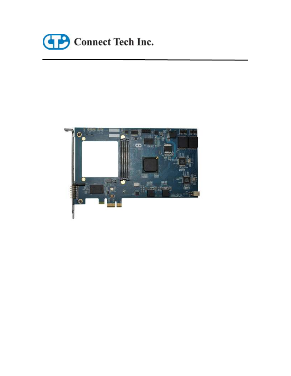
FreeForm/Express S6
PCIe Spartan-6 FMC Carrier
User Manual
Connect Tech Inc.
42 Arrow Road
Guelph, Ontario
N1K 1S6
Tel: 519-836-1291
Toll: 800-426-8979 (North America only)
Fax: 519-836-4878
Email: sales@connecttech.com
support@connecttech.com
Web: www.connecttech.com
CTIM-00060 | Revision 0.01 | 2011/06/27
Page 2

Connect Tech Inc. | FreeForm/Express S6 - PCIe Spartan-6 FMC Carrier | User Manual
Table of Contents
Customer Support Overview .......................................................................................................................... 3
Contact Information........................................................................................................................................ 3
Limited Lifetime Warranty ............................................................................................................................. 4
Copyright Notice ............................................................................................................................................ 4
Trademark Acknowledgment ......................................................................................................................... 4
Revision History ............................................................................................................................................. 4
Introduction .................................................................................................................................................... 5
Features ..................................................................................................................................................................... 5
What is an FPGA Mezzanine Card (FMC)?.............................................................................................................. 5
System Block Diagram ............................................................................................................................................. 6
Hardware Description ..................................................................................................................................... 7
FPGA ........................................................................................................................................................................ 7
Description ..................................................................................................................................................... 7
PCI Express Bus ....................................................................................................................................................... 7
Description ..................................................................................................................................................... 7
Memory & Flash ....................................................................................................................................................... 7
Description ..................................................................................................................................................... 7
Low Pin Count FMC Interface .................................................................................................................................. 7
Description ..................................................................................................................................................... 7
Connector ....................................................................................................................................................... 8
Configuration .......................................................................................................................................................... 12
Ethernet ................................................................................................................................................................... 13
Description ....................................................................................................................................................13
Connector & LEDs .......................................................................................................................................13
Serial ....................................................................................................................................................................... 15
Description ....................................................................................................................................................15
Connectors ....................................................................................................................................................15
Power ...................................................................................................................................................................... 15
Description ....................................................................................................................................................15
Connectors & Jumpers ..................................................................................................................................15
Hardware Installation ....................................................................................................................................16
Standard computer .................................................................................................................................................. 16
Cables & Interconnect ...................................................................................................................................17
Mating Cables ......................................................................................................................................................... 17
Mating Connectors .................................................................................................................................................. 17
FPGA Design ................................................................................................................................................18
FPGA Pinout .................................................................................................................................................19
Specifications ................................................................................................................................................25
Revision 0.01 2
Page 3

Connect Tech Inc. | FreeForm/Express S6 - PCIe Spartan-6 FMC Carrier | User Manual
Customer Support Overview
If you experience difficulties after reading the manual and/or using the product, contact the
Connect Tech reseller from which you purchased the product. In most cases the reseller can help
you with product installation and difficulties.
In the event that the reseller is unable to resolve your problem, our highly qualified support staff
can assist you. Our support section is available 24 hours a day, 7 days a week on our website at:
www.connecttech.com/sub/support/support.asp. See the contact information section below for
more information on how to contact us directly. Our technical support is always free.
Contact Information
We offer three ways for you to contact us:
Mail/Courier
You may contact us by letter at:
Connect Tech Inc.
Technical Support
42 Arrow Road
Guelph, Ontario
Canada N1K 1S6
Email/Internet
You may contact us through the Internet. Our email and URL addresses on the Internet are:
sales@connecttech.com
support@connecttech.com
www.connecttech.com
Note:
Please go to the Download Zone or the Knowledge Database in the Support Center on the Connect
Tech website for product manuals, installation guides, device driver software and technical tips.
Submit your technical support questions to our customer support engineers via the Support Center
on the Connect Tech website.
Telephone/Facsimile
Technical Support representatives are ready to answer your call Monday through Friday, from
8:30 a.m. to 5:00 p.m. Eastern Standard Time. Our numbers for calls are:
Toll Free: 800-426-8979 (North America only)
Telephone: 519-836-1291 (Live assistance available 8:30 a.m. to 5:00 p.m. EST,
Monday to Friday)
Facsimile: 519-836-4878 (on-line 24 hours)
Revision 0.01 3
Page 4

Connect Tech Inc. | FreeForm/Express S6 - PCIe Spartan-6 FMC Carrier | User Manual
Limited Lifetime Warranty
Connect Tech Inc. provides a Lifetime Warranty for all Connect Tech Inc. products. Should this
product, in Connect Tech Inc.'s opinion, fail to be in good working order during the warranty
period, Connect Tech Inc. will, at its option, repair or replace this product at no charge, provided
that the product has not been subjected to abuse, misuse, accident, disaster or non-Connect Tech
Inc. authorized modification or repair.
You may obtain warranty service by delivering this product to an authorized Connect Tech Inc.
business partner or to Connect Tech Inc. along with proof of purchase. Product returned to
Connect Tech Inc. must be pre-authorized by Connect Tech Inc. with an RMA (Return Material
Authorization) number marked on the outside of the package and sent prepaid, insured and
packaged for safe shipment. Connect Tech Inc. will return this product by prepaid ground
shipment service.
The Connect Tech Inc. Lifetime Warranty is defined as the serviceable life of the product. This is
defined as the period during which all components are available. Should the product prove to be
irreparable, Connect Tech Inc. reserves the right to substitute an equivalent product if available or
to retract Lifetime Warranty if no replacement is available.
The above warranty is the only warranty authorized by Connect Tech Inc. Under no
circumstances will Connect Tech Inc. be liable in any way for any damages, including any lost
profits, lost savings or other incidental or consequential damages arising out of the use of, or
inability to use, such product.
Copyright Notice
The information contained in this document is subject to change without notice. Connect Tech
Inc. shall not be liable for errors contained herein or for incidental consequential damages in
connection with the furnishing, performance, or use of this material. This document contains
proprietary information that is protected by copyright. All rights are reserved. No part of this
document may be photocopied, reproduced, or translated to another language without the prior
written consent of Connect Tech Inc.
Copyright 1997 - 2011 by Connect Tech Inc.
Trademark Acknowledgment
Connect Tech Inc. acknowledges all trademarks, registered trademarks and/or copyrights referred
to in this document as the property of their respective owners.
Not listing all possible trademarks or copyright acknowledgments does not constitute a lack of
acknowledgment to the rightful owners of the trademarks and copyrights mentioned in this
document.
Revision History
Revision 0.00e – 2011/01/26
Revision 0.00f – 2011/03/28
Revision 0.00g – 2011/06/27
Revision 0.01 4
Page 5

Connect Tech Inc. | FreeForm/Express S6 - PCIe Spartan-6 FMC Carrier | User Manual
Introduction
Connect Tech’s FreeForm/Express S6 is a reconfigurable computing platform that is based on the
Xilinx Spartan-6 FPGA; featuring integrated PCI Express® blocks, advanced memory support,
and 3.125 Gbps low-power transceivers. The FreeForm/Express S6 includes an industry-standard
FPGA Mezzanine Card (FMC) connector, which provides a flexible I/O interface for future
scaling and customization. The PCIe bus bandwidth ensures high speed communication between
the host system and the application’s interfaces.
A wide range of available FMC modules adds interfaces such as ADC and digital video, which
makes the FreeForm/Express S6 a highly versatile platform for system development. It is ideally
suited for applications requiring both prototyping and field deployment including real-time data
acquisition, high performance video processing, and software defined radio. The
FreeForm/Express S6 is optimized for embedded processor designs, supporting development with
Xilinx’s MicroBlaze.
Features
Spartan-6 LX45T FPGA
PCIe x1 form factor
128MB DDR3 Memory
Low Pin Count FMC connector
o 36 LVDS pairs
o 1 Rocket I/O channel
o I2C interface
2x 10/100/1000 Ethernet ports
1x RS-232 port
4 MB Flash for FPGA configuration
2 MB Flash for embedded code storage
200 MHz oscillator
JTAG debugging
Industrial temperature (-40 to 85C)
Lifetime warranty and free technical support.
What is an FPGA Mezzanine Card (FMC)?
An FPGA Mezzanine Card (FMC) is a standard created by VITA (VMEbus International Trade
Association). The FMC standard (VITA 57.1) defines a module size and connector interface with
generic reconfigurable I/O, making it perfect for FPGA daughter board applications. The standard
defines two pin-outs, low pin count (LPC) and high pin count (HPC); with each type using the
same connector form factor.
For more information visit http://www.vita.com/fmc.html.
Revision 0.01 5
Page 6
Connect Tech Inc. | FreeForm/Express S6 - PCIe Spartan-6 FMC Carrier | User Manual
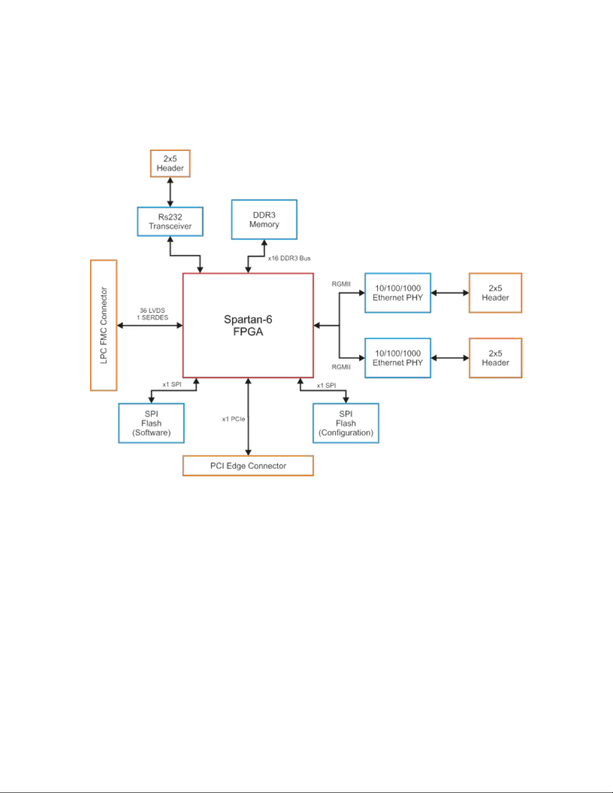
System Block Diagram
The following block diagram depicts component and connector interconnect, along with the appropriate
bus definitions.
Revision 0.01 6
Page 7

Connect Tech Inc. | FreeForm/Express S6 - PCIe Spartan-6 FMC Carrier | User Manual
Hardware Description
FPGA
Description
The FreeForm/Express S6 features the Xilinx Spartan-6 LX45T FPGA in a 484 pin BGA package
(Xilinx XC6SLX45T-2FGG484I). The Spartan-6 simplifies FPGA design by providing a
integrated memory controller and PCI express end point, along with high performance general I/O,
clocking, and internal memory resources comparable to be previous generation Virtex-class
FPGAs.
For more details on the Spartan-6 capabilities, visit:
http://www.xilinx.com/products/spartan6/index.htm.
PCI Express Bus
Description
The FreeForm/Express S6 has a single x1 PCIe express lane, connected directly to the Spartan-6
FPGA. The PCIe interface is facilitated by the Spartan-6’s integrated PCI express endpoint.
Memory & Flash
Description
A single 1024 Mbit x16 DDR3 component (Micron MT41J64M16JT-15E) is connected to the
Spartan-6 FPGA, providing 128 MB of high speed memory. The Spartan-6’s integrated memory
controller provides a generic high speed interface to FPGA logic.
In addition, a 16 Mbit SPI flash component (Numonyx M25P16) is connected to the FPGA’s user
I/O for storage of embedded processor code.
Low Pin Count FMC Interface
Description
The FreeForm/Express S6 provides a single Low Pin Count FPGA Mezzanine Card (FMC) Interface.
The LPC connector provides the following features
36 LVDS pairs, 2 designated as global clocks (or 68 2.5V LVCMOS pairs)
I2C interface
1 SERDES TX / RX channel (Rocket I/O , GTP), with clock
Power : +12VDC, +3.3V DC, +2.5V DC
The FreeForm/Express S6 LPC implementation differs from the VITA 57.1 specification as follows:
VADJ is fixed to +2.5 V DC
Only LVDS or 2.5V LVCMOS I/O is supported.
Revision 0.01 7
Page 8
Function
LPC FMC
Location
P7
Type
Samtec ASP-134603-01
Pinout
Pin
Signal
Description
C1
GND
Digital Ground
C2
DP0_C2M_P
Serdes pair from FPGA
C3
DP0_C2M_N
Serdes pair from FPGA
C4
GND
Digital Ground
C5
GND
Digital Ground
C6
DP0_M2C_P
Serdes pair to FPGA
C7
DP0_M2C_N
Serdes pair to FPGA
C8
GND
Digital Ground
C9
GND
Digital Ground
C10
LA06_P
LVDS pair
C11
LA06_N
LVDS pair
C12
GND
Digital Ground
C13
GND
Digital Ground
C14
LA10_P
LVDS pair
C15
LA10_N
LVDS pair
C16
GND
Digital Ground
C17
GND
Digital Ground
C18
LA14_P
LVDS pair
C19
LA14_N
LVDS pair
C20
GND
Digital Ground
C21
GND
Digital Ground
C22
LA18_P_CC
LVDS clock capable pair
C23
LA18_N_CC
LVDS clock capable pair
C24
GND
Digital Ground
C25
GND
Digital Ground
C26
LA27_P
LVDS pair
C27
LA27_N
LVDS pair
C28
GND
Digital Ground
C29
GND
Digital Ground
C30
SCL
I2C clock
C31
SDA
I2C data
C32
GND
Digital Ground
C33
GND
Digital Ground
C34
GA0
I2C address
C35
12P0V
+12V DC
Connect Tech Inc. | FreeForm/Express S6 - PCIe Spartan-6 FMC Carrier | User Manual
Connector
Revision 0.01 8
Page 9

Connect Tech Inc. | FreeForm/Express S6 - PCIe Spartan-6 FMC Carrier | User Manual
C36
GND
Digital Ground
C37
12P0V
+12V DC
C38
GND
Digital Ground
C39
3P3V
+3.3V DC
C40
GND
Digital Ground
D1
PG_C2M
Power good
D2
GND
Digital Ground
D3
GND
Digital Ground
D4
GBTCLK0_M2C_P
Serdes clock to FPGA
D5
GBTCLK0_M2C_N
Serdes clock to FPGA
D6
GND
Digital Ground
D7
GND
Digital Ground
D8
LA01_P_CC
LVDS clock capable pair
D9
LA01_N_CC
LVDS clock capable pair
D10
GND
Digital Ground
D11
LA05_P
LVDS pair
D12
LA05_N
LVDS pair
D13
GND
Digital Ground
D14
LA09_P
LVDS pair
D15
LA09_N
LVDS pair
D16
GND
Digital Ground
D17
LA13_P
LVDS pair
D18
LA13_N
LVDS pair
D19
GND
Digital Ground
D20
LA17_P_CC
LVDS clock capable pair
D21
LA17_N_CC
LVDS clock capable pair
D22
GND
Digital Ground
D23
LA23_P
LVDS pair
D24
LA23_N
LVDS pair
D25
GND
Digital Ground
D26
LA26_P
LVDS pair
D27
LA26_N
LVDS pair
D28
GND
Digital Ground
D29
TCK
JTAG
D30
TDI
JTAG
D31
TDO
JTAG
D32
3P3VAUX
+3.3V DC
D33
TMS
JTAG
D34
TRST_L
JTAG
D35
GA1
I2C address
D36
3P3V
+3.3V DC
D37
GND
Digital Ground
D38
3P3V
+3.3V DC
Revision 0.01 9
Page 10

Connect Tech Inc. | FreeForm/Express S6 - PCIe Spartan-6 FMC Carrier | User Manual
D39
GND
Digital Ground
D40
3P3V
+3.3V DC
G1
GND
Digital Ground
G2
CLK1_M2C_P
LVDS clock to FPGA
G3
CLK1_M2C_N
LVDS clock to FPGA
G4
GND
Digital Ground
G5
GND
Digital Ground
G6
LA00_P_CC
LVDS clock capable pair
G7
LA00_N_CC
LVDS clock capable pair
G8
GND
Digital Ground
G9
LA03_P
LVDS pair
G10
LA03_N
LVDS pair
G11
GND
Digital Ground
G12
LA08_P
LVDS pair
G13
LA08_N
LVDS pair
G14
GND
Digital Ground
G15
LA12_P
LVDS pair
G16
LA12_N
LVDS pair
G17
GND
Digital Ground
G18
LA16_P
LVDS pair
G19
LA16_N
LVDS pair
G20
GND
Digital Ground
G21
LA20_P
LVDS pair
G22
LA20_N
LVDS pair
G23
GND
Digital Ground
G24
LA22_P
LVDS pair
G25
LA22_N
LVDS pair
G26
GND
Digital Ground
G27
LA25_P
LVDS pair
G28
LA25_N
LVDS pair
G29
GND
Digital Ground
G30
LA29_P
LVDS pair
G31
LA29_N
LVDS pair
G32
GND
Digital Ground
G33
LA31_P
LVDS pair
G34
LA31_N
LVDS pair
G35
GND
Digital Ground
G36
LA33_P
LVDS pair
G37
LA33_N
LVDS pair
G38
GND
Digital Ground
G39
VADJ
+2.5V DC
G40
GND
Digital Ground
H1
VREF_A_M2C
Not used
Revision 0.01 10
Page 11

Connect Tech Inc. | FreeForm/Express S6 - PCIe Spartan-6 FMC Carrier | User Manual
H2
PRSNT_M2C_L
Present signal to FPGA
H3
GND
Digital Ground
H4
CLK0_M2C_P
LVDS clock to FPGA
H5
CLK0_M2C_N
LVDS clock to FPGA
H6
GND
Digital Ground
H7
LA02_P
LVDS pair
H8
LA02_N
LVDS pair
H9
GND
Digital Ground
H10
LA04_P
LVDS pair
H11
LA04_N
LVDS pair
H12
GND
Digital Ground
H13
LA07_P
LVDS pair
H14
LA07_N
LVDS pair
H15
GND
Digital Ground
H16
LA11_P
LVDS pair
H17
LA11_N
LVDS pair
H18
GND
Digital Ground
H19
LA15_P
LVDS pair
H20
LA15_N
LVDS pair
H21
GND
Digital Ground
H22
LA19_P
LVDS pair
H23
LA19_N
LVDS pair
H24
GND
Digital Ground
H25
LA21_P
LVDS pair
H26
LA21_N
LVDS pair
H27
GND
Digital Ground
H28
LA24_P
LVDS pair
H29
LA24_N
LVDS pair
H30
GND
Digital Ground
H31
LA28_P
LVDS pair
H32
LA28_N
LVDS pair
H33
GND
Digital Ground
H34
LA30_P
LVDS pair
H35
LA30_N
LVDS pair
H36
GND
Digital Ground
H37
LA32_P
LVDS pair
H38
LA32_N
LVDS pair
H39
GND
Digital Ground
H40
VADJ
+2.5V DC
Revision 0.01 11
Page 12

Connect Tech Inc. | FreeForm/Express S6 - PCIe Spartan-6 FMC Carrier | User Manual
Function
JTAG programming
Location
P5
Type
1x7 0.100” header
Samtec TSW-107-08-F-S-RA
Pinout
Pin
Signal
Description
1
TRST#
Reset, not used by Xilinx
products
2
TMS
Select
3
TDI
Data In
4
TDO
Data Out
5
TCK
Clock
6
GND
Digital Ground
7
VCC
Chain power, 3.3V
Function
Manual Reset
Pulls the Spartan-6 PROG_B pin to ground, resetting and
reconfiguring the FPGA
Location
J1
Type
1x2 0.100” jumper block
Pinout
Position
Description
1-2
+5V
off
floating
Default
Floating
Configuration
The FreeForm/Express S6 is designed so that the Spartan-6 configuration image is automatically loaded
from the on-board SPI flash at power- up. When a valid configuration is loaded, led D4 is illuminated.
JTAG configuration can be used at any time to program the FPGA.
The FreeForm/Express S6 is fitted with a x4 32 Mbit SPI flash (Winbond W25Q32BVSFIG), which can be
programmed indirectly via JTAG using Xilinx’s IMPACT.
Revision 0.01 12
Page 13

Connect Tech Inc. | FreeForm/Express S6 - PCIe Spartan-6 FMC Carrier | User Manual
Function
Hot Swap
When the is being configured, FPGA I/Os will be pulled
high with weak internal pull-ups
Location
J2
Type
1x2 0.100” jumper block
Pinout
Position
Description
1-2
I/Os have pullups
off
I/Os are floating
Default
Floating
Function
FMC JTAG Bypass
Selects either whether or not to include the FMC module
in the JTA chain
Location
J3
Type
2x2 0.100” jumper block
Pinout
Position
Description
1-3
TDI to FMC
2-4
TDO from FMC
3-4
Bypass
off
Not applicable
Default
Bypass
Function
Ethernet
Location
P6A, P6B
Type
2x5 2mm header
MLE TSHSM-205-D-06-G-V-L (or equivalent)
Ethernet
Description
Two 10/100/1000 Ethernet ports are connected to the FPGA, via two separate RGMII capable Ethernet
physical layer devices (PHYs). The FPGA logic resources are used to implement the Ethernet media
access controller (MAC).
Connector & LEDs
Revision 0.01 13
Page 14

Connect Tech Inc. | FreeForm/Express S6 - PCIe Spartan-6 FMC Carrier | User Manual
Pinout
Pin
Signal
Description
Pin
Signal
Description
1
MX1-
Data
2
MX1+
Data
3
MX2-
Data
4
MX2+
Data
5
FGND
Frame
Ground
6
FGND
Frame
Ground
7
MX3-
Data
8
MX3+
Data
9
MX4-
Data
10
MX4+
Data
Function
Ethernet Status LEDs
Locations
Pin
Signal
D16A
ETH0 Activity
D17A
ETH0 Link
D16B
ETH1 Activity
D17B
ETH1 Link
Revision 0.01 14
Page 15

Connect Tech Inc. | FreeForm/Express S6 - PCIe Spartan-6 FMC Carrier | User Manual
Function
RS232
Locations
P4
Type
2x5 0.100” header
Samtec TSW-105-07-L-D
Pinout
Pin
Signal
Pin
Signal
1
N/C 2 N/C 3 RXD1
4
RTS1
5
TXD1
6
CTS1 7 N/C 8 N/C 9 GND
10
N/C
Function
Standalone power
Location
P1
Type
2x3 0.100” power header, shrouded
Samtec IPL1-103-01-L-D-RA-K
Pinout
Pin
Signal
Description
1
GND
Digital Ground
2
GND
Digital Ground
3
GND
Digital Ground
4
+3.3V
+3.3V DC, used by circuitry and
power regulators
5
+3.3V
+3.3V DC, used by circuitry and
power regulators
6
+12V
+12V DC used by FMC module,
and power good circuit
Serial
Description
A standard RS232 serial ports is provided on P4, with UART implementation provided by FPGA logic.
Connectors
Power
Description
The FreeForm/Express S6 is designed to be powered from the PCIe bus. The board requires +3.3V DC for
all circuitry. +12VDC is required for the FMC power good signal and as the FMC module’s power source.
The FreeForm/Express S6 generates all other required power rails on-board.
In addition, a programming / desktop debugging standalone power connector P1 is provided.
WARNING: Do not plug the FreeForm/Express S6 into a PCIe slot with an external power source
connected to P1. This could lead to board damage and void the product warranty.
Connectors & Jumpers
Revision 0.01 15
Page 16

Connect Tech Inc. | FreeForm/Express S6 - PCIe Spartan-6 FMC Carrier | User Manual
Hardware Installation
Standard computer
1. Ensure all computer power supplies are off and disconnected (remove AC line cord)
2. Install the FMC module, if required.
3. Verify all jumper settings from the relevant sections
4. Install the necessary cables for the application.
WARNING: Do not plug the FreeForm/Express S6 into a PCIe slot with an external power source
connected to P1. This could lead to board damage and void the product warranty.
5. Install the FreeForm/Express S6 module into x1 PCIe slot.
6. Connect the appropriate interface cables to the FMC bracket I/O.
7. Connect the computer’s AC line cord to the computer’s power supply.
8. Turn on the computer system.
Revision 0.01 16
Page 17

Connect Tech Inc. | FreeForm/Express S6 - PCIe Spartan-6 FMC Carrier | User Manual
Description
Location
PCB Connector
Cable Part Number
[Drawing Number]
PCB End
Interface End
Power
P1
Samtec
IPL1-103-01-L-D-RA-K
Samtec
MMSD-03-20-L-03.25-S-K
2x3 IPD
Un-terminated
Serial
P4
Samtec
TSW-105-07-L-D
CAG104
[ CTIC-00048 ]
2x5 0.100” IDC
DB-9
GBE
P6A, P6B
MLE
TSHSM-205-D-06-G-V-L
CBG065
[CTIC-00181 ]
2x5 2mm socket
RJ45 socket
Description
Location
PCB Connector
Mating Connector
Note
FMC
P7
Samtec ASP-134603-01
Samtec
ASP-134604-01
10 mm stack
Samtec
ASP-134606-01
8.5 mm stack
Cables & Interconnect
Mating Cables
Cable drawings are available upon request
Mating Connectors
Revision 0.01 17
Page 18

Connect Tech Inc. | FreeForm/Express S6 - PCIe Spartan-6 FMC Carrier | User Manual
Function
IP
Version
Note
Memory
MIG
3.6
Rocket I/O
Spartan-6 FPGA GTP
Transceiver Wizard
1.7 PCIe
Spartan-6 Integrated
Block for PCI Express
1.4 Ethernet
Tri Mode Ethernet MAC
4.4
A valid license is required to use this IP, contact Xilinx
for details
FPGA Design
In general, FPGA designs developed for the FreeForm/Express S6 can be based on IP generated with
Xilinx’s CORE Generator. The following table lists the CORE Generator IP proven to be compatible,
along with their current versions numbers.
For the latest reference designs developed by Connect Tech Inc., visit http://devel.connecttech.com
Revision 0.01 18
Page 19

Connect Tech Inc. | FreeForm/Express S6 - PCIe Spartan-6 FMC Carrier | User Manual
Pin Number
Signal Name
Pin Name
IO Standard
Bank
V20
cfg_busy
IO_L74N_DOUT_BUSY_1
LVCMOS25*
1
Y20
cfg_cclk
IO_L1P_CCLK_2
LVCMOS25*
2
AB20
cfg_csi_b_mosi_miso0
IO_L3N_MOSI_CSI_B_MISO0_2
LVCMOS25*
2
AA3
cfg_cso_b_csn
IO_L65N_CSO_B_2
LVCMOS25*
2
AA20
cfg_d0_miso1
IO_L3P_D0_DIN_MISO_MISO1_2
LVCMOS25*
2
R13
cfg_d1_miso2
IO_L12P_D1_MISO2_2
LVCMOS25*
2
T14
cfg_d2_miso3
IO_L12N_D2_MISO3_2
LVCMOS25*
2
AA6
cfg_d3
IO_L49P_D3_2
LVCMOS25*
2
AB6
cfg_d4
IO_L49N_D4_2
LVCMOS25*
2
Y5
cfg_d5
IO_L62P_D5_2
LVCMOS25*
2
AB5
cfg_d6
IO_L62N_D6_2
LVCMOS25*
2
W9
cfg_d7
IO_L48P_D7_2
LVCMOS25*
2
C3
cfg_hswapen
IO_L1P_HSWAPEN_0
LVCMOS25*
0
Y4
cfg_init_b
IO_L65P_INIT_B_2
LVCMOS25*
2
AA21
cfg_m0
IO_L1N_M0_CMPMISO_2
LVCMOS25*
2
Y8
cfg_rdwr_b
IO_L48N_RDWR_B_VREF_2
LVCMOS25*
2
K2
ddr3_a<0>
IO_L47P_M3A0_3
SSTL15_II
3
K1
ddr3_a<1>
IO_L47N_M3A1_3
SSTL15_II
3
K5
ddr3_a<2>
IO_L49N_M3A2_3
SSTL15_II
3
M6
ddr3_a<3>
IO_L45P_M3A3_3
SSTL15_II
3
H3
ddr3_a<4>
IO_L51N_M3A4_3
SSTL15_II
3
M3
ddr3_a<5>
IO_L44P_GCLK21_M3A5_3
SSTL15_II
3
L4
ddr3_a<6>
IO_L44N_GCLK20_M3A6_3
SSTL15_II
3
K6
ddr3_a<7>
IO_L49P_M3A7_3
SSTL15_II
3
G3
ddr3_a<8>
IO_L52P_M3A8_3
SSTL15_II
3
G1
ddr3_a<9>
IO_L52N_M3A9_3
SSTL15_II
3
J4
ddr3_a<10>
IO_L51P_M3A10_3
SSTL15_II
3
E1
ddr3_a<11>
IO_L54N_M3A11_3
SSTL15_II
3
F1
ddr3_a<12>
IO_L53N_M3A12_3
SSTL15_II
3
J6
ddr3_a<13>
IO_L55P_M3A13_3
SSTL15_II
3
H5
ddr3_a<14>
IO_L55N_M3A14_3
SSTL15_II
3
J3
ddr3_ba<0>
IO_L48P_M3BA0_3
SSTL15_II
3
J1
ddr3_ba<1>
IO_L48N_M3BA1_3
SSTL15_II
3
H1
ddr3_ba<2>
IO_L50N_M3BA2_3
SSTL15_II
3
M4
ddr3_cas_n
IO_L43N_GCLK22_IRDY2_M3CASN_3
SSTL15_II
3
K3
ddr3_ck_n
IO_L46N_M3CLKN_3
DIFF_SSTL15_II
3
FPGA Pinout
The following table lists the FPGA pin (ball) to signal mapping. The standard Spartan-6 pin name is listed,
along with the I/O standard used and bank number.
Revision 0.01 19
Page 20

Connect Tech Inc. | FreeForm/Express S6 - PCIe Spartan-6 FMC Carrier | User Manual
Pin Number
Signal Name
Pin Name
IO Standard
Bank
K4
ddr3_ck_p
IO_L46P_M3CLK_3
DIFF_SSTL15_II
3
F2
ddr3_cke
IO_L53P_M3CKE_3
SSTL15_II
3
N4
ddr3_dm
IO_L42N_GCLK24_M3LDM_3
SSTL15_II
3
R3
ddr3_dq<0>
IO_L37P_M3DQ0_3
SSTL15_II
3
R1
ddr3_dq<1>
IO_L37N_M3DQ1_3
SSTL15_II
3
P2
ddr3_dq<2>
IO_L38P_M3DQ2_3
SSTL15_II
3
P1
ddr3_dq<3>
IO_L38N_M3DQ3_3
SSTL15_II
3
L3
ddr3_dq<4>
IO_L41P_GCLK27_M3DQ4_3
SSTL15_II
3
L1
ddr3_dq<5>
IO_L41N_GCLK26_M3DQ5_3
SSTL15_II
3
M2
ddr3_dq<6>
IO_L40P_M3DQ6_3
SSTL15_II
3
M1
ddr3_dq<7>
IO_L40N_M3DQ7_3
SSTL15_II
3
T2
ddr3_dq<8>
IO_L36P_M3DQ8_3
SSTL15_II
3
T1
ddr3_dq<9>
IO_L36N_M3DQ9_3
SSTL15_II
3
U3
ddr3_dq<10>
IO_L35P_M3DQ10_3
SSTL15_II
3
U1
ddr3_dq<11>
IO_L35N_M3DQ11_3
SSTL15_II
3
W3
ddr3_dq<12>
IO_L33P_M3DQ12_3
SSTL15_II
3
W1
ddr3_dq<13>
IO_L33N_M3DQ13_3
SSTL15_II
3
Y2
ddr3_dq<14>
IO_L32P_M3DQ14_3
SSTL15_II
3
Y1
ddr3_dq<15>
IO_L32N_M3DQ15_3
SSTL15_II
3
N1
ddr3_dqs_n
IO_L39N_M3LDQSN_3
DIFF_SSTL15_II
3
N3
ddr3_dqs_p
IO_L39P_M3LDQS_3
DIFF_SSTL15_II
3
L6
ddr3_odt
IO_L45N_M3ODT_3
SSTL15_II
3
M5
ddr3_ras_n
IO_L43P_GCLK23_M3RASN_3
SSTL15_II
3
E3
ddr3_reset_n
IO_L54P_M3RESET_3
LVCMOS15
3
P3
ddr3_udm
IO_L42P_GCLK25_TRDY2_M3UDM_3
SSTL15_II
3
V1
ddr3_udqs_n
IO_L34N_M3UDQSN_3
DIFF_SSTL15_II
3
V2
ddr3_udqs_p
IO_L34P_M3UDQS_3
DIFF_SSTL15_II
3
H2
ddr3_we_n
IO_L50P_M3WE_3
SSTL15_II
3
G11
fmc_clk0_m2c_n
IO_L35N_GCLK16_0
LVDS_25
0
H12
fmc_clk0_m2c_p
IO_L35P_GCLK17_0
LVDS_25
0
F16
fmc_clk1_m2c_n
IO_L37N_GCLK12_0
LVDS_25
0
E16
fmc_clk1_m2c_p
IO_L37P_GCLK13_0
LVDS_25
0
A8
fmc_dp0_c2m_n
MGTTXN1_101
B8
fmc_dp0_c2m_p
MGTTXP1_101
C9
fmc_dp0_m2c_n
MGTRXN1_101
D9
fmc_dp0_m2c_p
MGTRXP1_101
D11
fmc_gbtclk0_m2c_n
MGTREFCLK1N_101
C11
fmc_gbtclk0_m2c_p
MGTREFCLK1P_101
T5
fmc_i2c_scl
IO_L7N_3
LVCMOS15
3
T6
fmc_i2c_sda
IO_L7P_3
LVCMOS15
3
Revision 0.01 20
Page 21

Connect Tech Inc. | FreeForm/Express S6 - PCIe Spartan-6 FMC Carrier | User Manual
Pin Number
Signal Name
Pin Name
IO Standard
Bank
AB11
fmc_la00_cc_n
IO_L32N_GCLK28_2
LVDS_25
2
Y11
fmc_la00_cc_p
IO_L32P_GCLK29_2
LVDS_25
2
AB12
fmc_la01_cc_n
IO_L31N_GCLK30_D15_2
LVDS_25
2
AA12
fmc_la01_cc_p
IO_L31P_GCLK31_D14_2
LVDS_25
2
AB4
fmc_la02_n
IO_L63N_2
LVDS_25
2
AA4
fmc_la02_p
IO_L63P_2
LVDS_25
2
AB7
fmc_la03_n
IO_L47N_2
LVDS_25
2
Y7
fmc_la03_p
IO_L47P_2
LVDS_25
2
R8
fmc_la04_n
IO_L59N_2
LVDS_25
2
R9
fmc_la04_p
IO_L59P_2
LVDS_25
2
U6
fmc_la05_n
IO_L64N_D9_2
LVDS_25
2
T7
fmc_la05_p
IO_L64P_D8_2
LVDS_25
2
Y6
fmc_la06_n
IO_L60N_2
LVDS_25
2
W6
fmc_la06_p
IO_L60P_2
LVDS_25
2
AB9
fmc_la07_n
IO_L43N_2
LVDS_25
2
Y9
fmc_la07_p
IO_L43P_2
LVDS_25
2
AB8
fmc_la08_n
IO_L45N_2
LVDS_25
2
AA8
fmc_la08_p
IO_L45P_2
LVDS_25
2
U8
fmc_la09_n
IO_L57N_2
LVDS_25
2
T8
fmc_la09_p
IO_L57P_2
LVDS_25
2
W8
fmc_la10_n
IO_L58N_2
LVDS_25
2
V7
fmc_la10_p
IO_L58P_2
LVDS_25
2
AB10
fmc_la11_n
IO_L41N_VREF_2
LVDS_25
2
AA10
fmc_la11_p
IO_L41P_2
LVDS_25
2
V9
fmc_la12_n
IO_L50N_2
LVDS_25
2
U9
fmc_la12_p
IO_L50P_2
LVDS_25
2
Y10
fmc_la13_n
IO_L44N_2
LVDS_25
2
W10
fmc_la13_p
IO_L44P_2
LVDS_25
2
W11
fmc_la14_n
IO_L42N_2
LVDS_25
2
V11
fmc_la14_p
IO_L42P_2
LVDS_25
2
Y12
fmc_la15_n
IO_L40N_2
LVDS_25
2
W12
fmc_la15_p
IO_L40P_2
LVDS_25
2
U10
fmc_la16_n
IO_L46N_2
LVDS_25
2
T10
fmc_la16_p
IO_L46P_2
LVDS_25
2
U12
fmc_la17_cc_n
IO_L29N_GCLK2_2
LVDS_25
2
T12
fmc_la17_cc_p
IO_L29P_GCLK3_2
LVDS_25
2
AB13
fmc_la18_cc_n
IO_L30N_GCLK0_USERCCLK_2
LVDS_25
2
Y13
fmc_la18_cc_p
IO_L30P_GCLK1_D13_2
LVDS_25
2
U13
fmc_la19_n
IO_L16N_VREF_2
LVDS_25
2
U14
fmc_la19_p
IO_L16P_2
LVDS_25
2
Revision 0.01 21
Page 22

Connect Tech Inc. | FreeForm/Express S6 - PCIe Spartan-6 FMC Carrier | User Manual
Pin Number
Signal Name
Pin Name
IO Standard
Bank
T11
fmc_la20_n
IO_L22N_2
LVDS_25
2
R11
fmc_la20_p
IO_L22P_2
LVDS_25
2
U15
fmc_la21_n
IO_L23N_2
LVDS_25
2
T15
fmc_la21_p
IO_L23P_2
LVDS_25
2
Y14
fmc_la22_n
IO_L20N_2
LVDS_25
2
W14
fmc_la22_p
IO_L20P_2
LVDS_25
2
W13
fmc_la23_n
IO_L18N_2
LVDS_25
2
V13
fmc_la23_p
IO_L18P_2
LVDS_25
2
AB15
fmc_la24_n
IO_L21N_2
LVDS_25
2
Y15
fmc_la24_p
IO_L21P_2
LVDS_25
2
AB14
fmc_la25_n
IO_L6N_2
LVDS_25
2
AA14
fmc_la25_p
IO_L6P_2
LVDS_25
2
V15
fmc_la26_n
IO_L4N_VREF_2
LVDS_25
2
U16
fmc_la26_p
IO_L4P_2
LVDS_25
2
W15
fmc_la27_n
IO_L17N_2
LVDS_25
2
Y16
fmc_la27_p
IO_L17P_2
LVDS_25
2
Y18
fmc_la28_n
IO_L5N_2
LVDS_25
2
W17
fmc_la28_p
IO_L5P_2
LVDS_25
2
W18
fmc_la29_n
IO_L2N_CMPMOSI_2
LVDS_25
2
V17
fmc_la29_p
IO_L2P_CMPCLK_2
LVDS_25
2
AB17
fmc_la30_n
IO_L15N_2
LVDS_25
2
Y17
fmc_la30_p
IO_L15P_2
LVDS_25
2
AB16
fmc_la31_n
IO_L19N_2
LVDS_25
2
AA16
fmc_la31_p
IO_L19P_2
LVDS_25
2
AB19
fmc_la32_n
IO_L13N_D10_2
LVDS_25
2
Y19
fmc_la32_p
IO_L13P_M1_2
LVDS_25
2
AB18
fmc_la33_n
IO_L14N_D12_2
LVDS_25
2
AA18
fmc_la33_p
IO_L14P_D11_2
LVDS_25
2
R16
fmc_prsnt_m2c_l
IO_L70N_1
LVCMOS25*
1
F10
main_clk_n
IO_L34N_GCLK18_0
LVDS_25
0
G9
main_clk_p
IO_L34P_GCLK19_0
LVDS_25
0
A2
mig_calib_done_led
IO_L3N_0
LVCMOS25*
0
E5
mig_error_led
IO_L4P_0
LVCMOS25*
0
R7
mig_rzq
IO_L1P_3
SSTL15_II
3
W4
mig_zio
IO_L2P_3
SSTL15_II
3
D5
pcie_perst
IO_L2N_0
LVCMOS25*
0
B10
pcie_refclk_n
MGTREFCLK0N_101
A10
pcie_refclk_p
MGTREFCLK0P_101
C7
pcie_rx_n
MGTRXN0_101
D7
pcie_rx_p
MGTRXP0_101
Revision 0.01 22
Page 23

Connect Tech Inc. | FreeForm/Express S6 - PCIe Spartan-6 FMC Carrier | User Manual
Pin Number
Signal Name
Pin Name
IO Standard
Bank
E6
pcie_stat_led<0>
IO_L4N_0
LVCMOS25*
0
B3
pcie_stat_led<1>
IO_L5P_0
LVCMOS25*
0
A3
pcie_stat_led<2>
IO_L5N_0
LVCMOS25*
0
A6
pcie_tx_n
MGTTXN0_101
B6
pcie_tx_p
MGTTXP0_101
M19
rgmii0_clk
IO_L40N_GCLK10_M1A6_1
LVCMOS25*
1
K19
rgmii0_intn
IO_L34P_A13_M1WE_1
LVCMOS25*
1
H20
rgmii0_mdc
IO_L33N_A14_M1A4_1
LVCMOS25*
1
J19
rgmii0_mdio
IO_L33P_A15_M1A10_1
LVCMOS25*
1
K17
rgmii0_resetn
IO_L36P_A9_M1BA0_1
LVCMOS25*
1
H21
rgmii0_rx_ctl
IO_L37P_A7_M1A0_1
LVCMOS25*
1
K22
rgmii0_rxc
IO_L41N_GCLK8_M1CASN_1
LVCMOS25*
1
H22
rgmii0_rxd<0>
IO_L37N_A6_M1A1_1
LVCMOS25*
1
G22
rgmii0_rxd<1>
IO_L35N_A10_M1A2_1
LVCMOS25*
1
F21
rgmii0_rxd<2>
IO_L31P_A19_M1CKE_1
LVCMOS25*
1
F22
rgmii0_rxd<3>
IO_L31N_A18_M1A12_1
LVCMOS25*
1
E22
rgmii0_tx_ctl
IO_L32N_A16_M1A9_1
LVCMOS25*
1
D22
rgmii0_txc
IO_L28N_VREF_1
LVCMOS25*
1
B21
rgmii0_txd<0>
IO_L10P_1
LVCMOS25*
1
B22
rgmii0_txd<1>
IO_L10N_1
LVCMOS25*
1
C22
rgmii0_txd<2>
IO_L20N_1
LVCMOS25*
1
D21
rgmii0_txd<3>
IO_L28P_1
LVCMOS25*
1
P20
rgmii1_clk
IO_L42P_GCLK7_M1UDM_1
LVCMOS25*
1
P21
rgmii1_intn
IO_L46P_FCS_B_M1DQ2_1
LVCMOS25*
1
U20
rgmii1_mdc
IO_L49P_M1DQ10_1
LVCMOS25*
1
T22
rgmii1_mdio
IO_L48N_M1DQ9_1
LVCMOS25*
1
T21
rgmii1_resetn
IO_L48P_HDC_M1DQ8_1
LVCMOS25*
1
R22
rgmii1_rx_ctl
IO_L47N_LDC_M1DQ1_1
LVCMOS25*
1
L22
rgmii1_rxc
IO_L43N_GCLK4_M1DQ5_1
LVCMOS25*
1
P22
rgmii1_rxd<0>
IO_L46N_FOE_B_M1DQ3_1
LVCMOS25*
1
N22
rgmii1_rxd<1>
IO_L45N_A0_M1LDQSN_1
LVCMOS25*
1
M22
rgmii1_rxd<2>
IO_L44N_A2_M1DQ7_1
LVCMOS25*
1
M21
rgmii1_rxd<3>
IO_L44P_A3_M1DQ6_1
LVCMOS25*
1
Y21
rgmii1_tx_ctl
IO_L52P_M1DQ14_1
LVCMOS25*
1
Y22
rgmii1_txc
IO_L52N_M1DQ15_1
LVCMOS25*
1
U22
rgmii1_txd<0>
IO_L49N_M1DQ11_1
LVCMOS25*
1
V22
rgmii1_txd<1>
IO_L50N_M1UDQSN_1
LVCMOS25*
1
V21
rgmii1_txd<2>
IO_L50P_M1UDQS_1
LVCMOS25*
1
W22
rgmii1_txd<3>
IO_L51N_M1DQ13_1
LVCMOS25*
1
R17
rs232_cts
IO_L72P_1
LVCMOS25*
1
Revision 0.01 23
Page 24

Connect Tech Inc. | FreeForm/Express S6 - PCIe Spartan-6 FMC Carrier | User Manual
Pin Number
Signal Name
Pin Name
IO Standard
Bank
P18
rs232_rts
IO_L71N_1
LVCMOS25*
1
T18
rs232_rx
IO_L73N_1
LVCMOS25*
1
T19
rs232_tx
IO_L73P_1
LVCMOS25*
1
A4
tmp
IO_L6N_0
LVCMOS25*
0
F7
user_led0
IO_L7P_0
LVCMOS25*
0
F8
user_led1
IO_L7N_0
LVCMOS25*
0
C5
user_led2
IO_L8P_0
LVCMOS25*
0
U19
X1_SPI_CLK
IO_L59P_1
LVCMOS25*
1
T17
X1_SPI_CSN
IO_L72N_1
LVCMOS25*
1
W20
X1_SPI_MISO
IO_L51P_M1DQ12_1
LVCMOS25*
1
P19
X1_SPI_MOSI
IO_L53P_1
LVCMOS25*
1
Revision 0.01 24
Page 25

Connect Tech Inc. | FreeForm/Express S6 - PCIe Spartan-6 FMC Carrier | User Manual
Form Factor
PCIe x1, half-length
FPGA
Spartan-6 LX45T FPGA
General Purpose I/O
Low Pin Count FMC connector
36 LVDS pairs
1 Rocket I/O channel
I2C interface
Memory
128MB DDR3 RAM
4 MB Flash for FPGA configuration
2 MB Flash for embedded code storage
Ethernet
2x Gigabit Ethernet Ports
Serial
1x RS-232
Temperature
-40 to 85C
[1]
Power
+3.3V DC, +12V DC required by some FMC
Power Consumption
TBD
Dimensions
4.375” x 6.600”
Weight
TBD
Warranty and Support
Lifetime warranty and free technical support
Specifications
[1] Actual operating temperature depends on the user FPGA configuration, refer to ISE reports for details
Revision 0.01 25
 Loading...