

Page 1

USER MANUAL
CANpro/104-Plus Opto
CTIM-00052 Revision 0.00 - April 23, 2009
Page 2

CANpro/104-Plus Opto User Manual
Copyright Notice
The information contained in this document is subject to change without notice. Connect Tech Inc. shall not
be liable for errors contained herein or for incidental consequential damages in connection with the furnishing,
performance, or use of this material. This document contains proprietary information that is protected by
copyright. All rights are reserved. No part of this document may be photocopied, reproduced, or translated to
another language without the prior written consent of Connect Tech, Inc.
Copyright © 2009 by Connect Tech Inc.
Trademark Acknowledgement
Connect Tech Inc. acknowledges all trademarks, registered trademarks and/or copyrights referred to in this
document as the property of their respective owners.
Not listing all possible trademarks or copyright acknowledgments does not constitute a lack of
acknowledgment to the rightful owners of the trademarks and copyrights mentioned in this document.
Revision History
Revision 0.00 April 23, 2009
Original Document
CTIM-00052 Revision 0.00 4/23/2009 www.connecttech.com 2
800-426-8979 | 519-836-1291
Page 3

CANpro/104-Plus Opto User Manual
Table of Contents
Copyright Notice ................................................................................................................................................ 2
Trademark Acknowledgement ................................................................................................ ............................ 2
Revision History ................................................................................................................................................. 2
Table of Contents ................................................................................................................................................ 3
Introduction......................................................................................................................................................... 4
Features ............................................................................................................................................................... 4
CANpro/104-Plus Opto Diagrams ...................................................................................................................... 5
Hardware Installation .......................................................................................................................................... 7
PCI Interrupt, Clock and ID Selection ........................................................................................................... 8
On-Board Jumper Configuration .................................................................................................................... 9
120 Ohm Termination Jumpers ................................................................................................................. 9
Slew Rate Control Jumpers ..................................................................................................................... 10
DB-9 Frame Ground Connect ................................................................................................................. 10
Connector Pinouts ............................................................................................................................................. 11
Software Configuration ..................................................................................................................................... 12
GPIO Details ..................................................................................................................................................... 18
GPIO Header ................................................................................................................................................ 18
GPIO Control and Addressing ..................................................................................................................... 19
Specifications .................................................................................................................................................... 20
Operating Environment ........................................................................................................................... 20
Power Requirements ............................................................................................................................... 20
PC Bus Interface...................................................................................................................................... 20
Optical/Power Isolation ................................................................ ................................ ........................... 20
Dimensions .............................................................................................................................................. 20
Connectors/Interface ............................................................................................................................... 20
GPIO ....................................................................................................................................................... 20
Certification ...................................................................................................................................................... 21
Certification for CANpro/104-Plus Opto ..................................................................................................... 21
Limited Lifetime Warranty ............................................................................................................................... 22
Customer Support Overview............................................................................................................................. 22
Contact Information ................................ ................................ ................................................................ .......... 22
3 www.connecttech.com CTIM-00052 Revision 0.00 4/23/2009
800-426-8979 | 519-836-1291
Page 4

CANpro/104-Plus Opto User Manual
Introduction
CANpro/104-Plus Opto combines the power of two independent NXP SJA1000 CAN controllers with 3kV
optical isolation to provide maximum protection for industrial control applications exposed to harsh
conditions. Based on the PCI bus and a PCI-104 form factor, CANpro/104-Plus Opto frees up valuable I/O
space for greater flexibility in your embedded system.
Features
● Two independent, industry standard NXP SJA1000 CAN controllers (2.0B compliant)
● PCI-104 2.2 compliant
● 16MHz SJA1000 input clock
● 32MHz local bus clock
● Fail-safe power-up/power-down using on-board impendence transceivers to maximize nodes on the bus
and ensure glitch-free operation.
● Supports up to 1.0 Mbps operation and over 120 nodes on the bus
● 3kV optical isolation for each port from the host system
● Output slew rate limiting for lower radiated emissions
● Memory mapped addressing to save valuable I/O space (no jumpers required)
● Decoded address range is configurable for BasicCAN and PeliCAN modes
● Two ten pin right angled headers as standard I/O connectors (DB-9 option available)
● GPIO: 8-bit 3.3V I/O header
● Operating temperature range of -40°C to 85°C
● +5V DC 500mA (max.) power output
RoHS compliant
CTIM-00052 Revision 0.00 4/23/2009 www.connecttech.com 4
800-426-8979 | 519-836-1291
Page 5
CANpro/104-Plus Opto User Manual
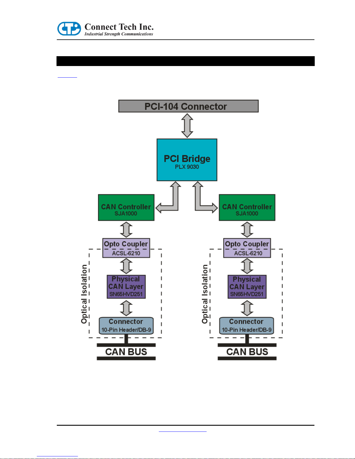
CANpro/104-Plus Opto Diagrams
Figure 1 illustrates the location of each component on the CANpro/104-Plus Opto.
Figure 1: CANpro/104-Plus Opto Block Diagram
5 www.connecttech.com CTIM-00052 Revision 0.00 4/23/2009
800-426-8979 | 519-836-1291
Page 6

CANpro/104-Plus Opto User Manual
Figure 2: CANpro/104-Plus Opto Board Diagram
CTIM-00052 Revision 0.00 4/23/2009 www.connecttech.com 6
800-426-8979 | 519-836-1291
Page 7

CANpro/104-Plus Opto User Manual
Hardware Installation
Before You Begin
Before you begin, take a minute to ensure that your package includes the required components that should
have shipped with your CANpro/104-Plus Opto.
● One CANpro/104-Plus Opto CAN controller board
● One CD containing documentation
If anything is missing, contact Connect Tech or your reseller. Also, visit the Download Zone of the Support
Center on the Connect Tech website for the latest product manuals, installation guides, diagnostic utilities and
device driver software.
Installing the CANpro/104-Plus Opto Into Your System
Turn off the power to your embedded computer and open any enclosures needed to access the PC/104-
Plus or PCI-104 expansion connectors.
Carefully insert the board into the PC/104-Plus or PCI-104 connector.
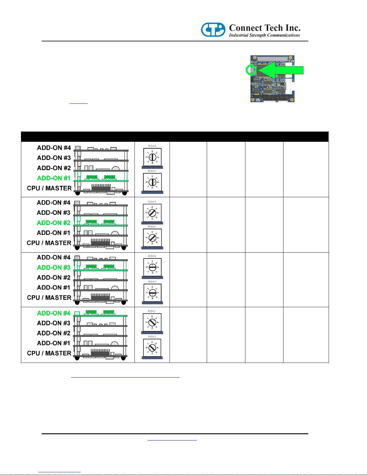
Set the ID rotary switch accordingly (see Table 1).
Set the correct on-board jumpers for each CAN port (J1 – J6) (see pages 9-10 for more details).
Power on your embedded computer and install the appropriate drivers for your operating system.
7 www.connecttech.com CTIM-00052 Revision 0.00 4/23/2009
800-426-8979 | 519-836-1291
Page 8
CANpro/104-Plus Opto User Manual
The following PCI signals, (INTA#, INTB# INTC# INTD#), (CLK0, CLK1,
CLK2, CLK3), (IDSEL0, IDSEL1, IDSEL2, IDSEL3), are selected by using the
Rotary Switch on the CANpro/104-Plus Opto board (RSW1). Selections need to
match the stack location of the CANpro/104-Plus Opto in your PC/104-Plus
stack. See Table 1 below for more details.
Rotary Switch Location
Stack Location
Rotary Setting
PCI INT#
PCI CLK
PCI IDSEL
0 or 4
INTA#
CLK0
IDSEL0
1 or 5
INTB#
CLK1
IDSEL1
2 or 6
INTC#
CLK2
IDSEL2
3 or 7
INTD#
CLK3
IDSEL3
PCI Interrupt, Clock and ID Selection
Table 1: Rotary Selection
Please visit http://www.pc104.org/pc104_plus_specs.php to request the full PC/104-Plus specification for
more details on signals.
CTIM-00052 Revision 0.00 4/23/2009 www.connecttech.com 8
800-426-8979 | 519-836-1291
Page 9

CANpro/104-Plus Opto User Manual
On-Board Jumper Configuration
Figure 3: CAN Ports and Jumper Locations
120 Ohm Termination Jumpers
Jumpers J1 and J4 will enable a 120 Ohm termination resistor across the CAN-H and CAN-L lines.
Termination is always recommended for improved signal integrity, especially for long transmission lines.
Termination requirements should be evaluated on a case by case basis. Typically both ends of a CAN bus are
terminated, but termination is not enabled on cards that sit in the middle of the bus. See Figure 4 and Figure 5
for examples that indicate when to use this jumper selection.
Figure 4: Example – CANpro/104-Plus Opto at the end of a CAN bus
NOTE:
The 120 Ohm termination jumper must be installed in this
situation.
9 www.connecttech.com CTIM-00052 Revision 0.00 4/23/2009
800-426-8979 | 519-836-1291
Page 10

CANpro/104-Plus Opto User Manual
Figure 5: Example CANpro/104-Plus Opto in the middle of the CAN bus
NOTE:
The 120 Ohm termination jumper does not need to be installed
in this situation.
Slew Rate Control Jumpers
Installing a jumper on J2 or J5 (see Figure 3) will disable slew rate limiting for the associated CAN port. Slew
rate limiting will reduce the emitted switching noise that is sent out onto the CAN bus lines and radiated from
those lines. Switching noise may cause EMI/EMC incompatibilities depending on the cabling used to support
the system. The use of slew rate limiting may aid in a system that is nearing the maximum limit of emissions.
Properly shielded cabling will also dramatically reduce emissions. Slew rate limiting may only be used on
busses operating at slower baud rates. With the jumper installed, full 1Mbps operation is possible.
DB-9 Frame Ground Connect
CANpro/104-Plus Opto models that have DB-9 connectors, will allow you optionally enable the Frame
Ground to be tied to ports isolated ground plane with J3 and J6.
CTIM-00052 Revision 0.00 4/23/2009 www.connecttech.com 10
800-426-8979 | 519-836-1291
Page 11
CANpro/104-Plus Opto User Manual
Pin No.
Signal
1
+5V
2
CAN-L
3
CAN GND (isolated or non)
4
N/C 5 N/C 6 CAN GND (isolated or non)
7
CAN-H
8
N/C 9 +5V
Male DB-9 Connector
1
5
6
9
Pin No.
Signal
1
+5V
2
CAN-GND (isolated or non)
3
CAN-L
4
CANH
5
CAN-GND (isolated or non)
6
NC 7 NC 8 +5V
9
NC
10
NC
7 5 3
1
2
4 6 8
Printed circuit board
9
10
10-pin header
View facing 10-pin header
Connector Pinouts
Table 2: DB-9 Cable Connector Pinouts
Boards that are populated with right angled 2x5 0.100” headers will include a cable (CAG104) that will
break out from the on-board 2x5 header to a DB-9 connector.
Table 3: 10-pin Header Pinouts
11 www.connecttech.com CTIM-00052 Revision 0.00 4/23/2009
800-426-8979 | 519-836-1291
Page 12

CANpro/104-Plus Opto User Manual
Software Configuration
The information provided below is intended for advanced users and developers that wish to create their own
custom drivers. Typical CANpro/104-Plus Opto users will used the driver provided by Connect Tech.
PCI Properties of CANpro/104-Plus Opto
The CANpro/104-Plus Opto card will appear in your system with the following PCI information:
Vender ID: 0x10b5
Device ID: 0x9030
SubVender ID: 0x12c4
SubVender Device ID: 0x900
CAN Controller Address Space
CAN controllers are mapped on the PLX 9030 PCI Base Address 2 (BAR2) to Local Address Space 0. This
address space is re-mapped to a local offset of 0x00. Each CAN controller is allotted 256 bytes of address
space. CAN controller #1 has a local address range of 0x000 - 0x0FF, while CAN controller #2 has a local
address range 0x100 – 0x1FF. See below for the full address/register allocation details in both BasicCAN and
PeliCAN modes.
CTIM-00052 Revision 0.00 4/23/2009 www.connecttech.com 12
800-426-8979 | 519-836-1291
Page 13

CANpro/104-Plus Opto User Manual
READ WRITE READ WRITE
0x000 CR CR CR CR
0x001 CMR CMR
0x002 SR SR
0x003 IR IR
0x004 AC AC
0x005 AM AM
0x006 BTR0 BTR0
0x007 BTR1 BTR1
0x008 OC OC
0x009 TEST TEST TEST TEST
0x00A TX Buffer Identifier Byte 1 TX Buffer I dentifi er Byte 1
0x00B TX Buffer Identifi er Byte 2 TX Buffer Identifier Byte 1
0x00C TX Buffer Data Byte 1 TX Buffer Data Byte 1
0x00D TX Buffer Data Byte 2 TX Buffer Data Byte 2
0x00E TX Buffer Data Byte 3 TX Buffer Data Byte 3
0x00F TX Buffer Da ta Byte 4 TX Buffer Data Byte 4
0x010 TX Buffer Data Byte 5 TX Buffer Data Byte 5
0x011 TX Buffer Data Byte 6 TX Buffer Data Byte 6
0x012 TX Buffer Data Byte 7 TX Buffer Data Byte 7
0x013 TX Buffer Data Byte 8 TX Buffer Data Byte 8
0x014 RX Buffer Identifi er Byte 1 RX Buffer Identifi er Byte 1 RX Buffer Identifier Byte 1 RX Buffer Identifier Byte 1
0x015 RX Buffer Identifi er Byte 2 RX Buffer Identifi er Byte 2 RX Buffer Identifier Byte 2 RX Buffer Identifier Byte 2
0x016 RX Buffer Data Byte 1 RX Buffer Data Byte 1 RX Buffer Data Byte 1 RX Buffer Data Byte 1
0x017 RX Buffer Data Byte 2 RX Buffer Data Byte 2 RX Buffer Data Byte 2 RX Buffer Data Byte 2
0x018 RX Buffer Data Byte 3 RX Buffer Data Byte 3 RX Buffer Data Byte 3 RX Buffer Data Byte 3
0x019 RX Buffer Data Byte 4 RX Buffer Data Byte 4 RX Buffer Data Byte 4 RX Buffer Data Byte 4
0x01A RX Buffer Data Byte 5 RX Buffer Data Byte 5 RX Buffer Data Byte 5 RX Buffer Data Byte 5
0x01B RX Buffer Data Byte 6 RX Buffer Data Byte 6 RX Buffer Data Byte 6 RX Buffer Da ta Byte 6
0x01C RX Buffer Data Byte 7 RX Buffer Data Byte 7 RX Buffer Data Byte 7 RX Buffer Data Byte 7
0x01D RX Buffer Data Byte 8 RX Buffer Data Byte 8 RX Buffer Data Byte 8 RX Buffer Data Byte 8
0x01E
0x01F CDR CDR CDR CDR
...
0x0FF
OPERATING MODE
RESET MODE
Table 4: CAN Controller #1 (BasicCAN)
13 www.connecttech.com CTIM-00052 Revision 0.00 4/23/2009
800-426-8979 | 519-836-1291
Page 14

CANpro/104-Plus Opto User Manual
READ WRITE READ WRITE
0x100 CR CR CR CR
0x101 CMR CMR
0x102 SR SR
0x103 IR IR
0x104 AC AC
0x105 AM AM
0x106 BTR0 BTR0
0x107 BTR1 BTR1
0x108 OC OC
0x109 TEST TEST TEST TEST
0x10A TX Buffer Identifier Byte 1 TX Buffer I dentifi er Byte 1
0x10B TX Buffer Identifi er Byte 2 TX Buffer Identifier Byte 1
0x10C TX Buffer Data Byte 1 TX Buffer Data Byte 1
0x10D TX Buffer Data Byte 2 TX Buffer Data Byte 2
0x10E TX Buffer Data Byte 3 TX Buffer Data Byte 3
0x10F TX Buffer Da ta Byte 4 TX Buffer Da ta Byte 4
0x110 TX Buffer Data Byte 5 TX Buffer Data Byte 5
0x111 TX Buffer Data Byte 6 TX Buffer Data Byte 6
0x112 TX Buffer Data Byte 7 TX Buffer Data Byte 7
0x113 TX Buffer Data Byte 8 TX Buffer Data Byte 8
0x114 RX Buffer Identifi er Byte 1 RX Buffer Identifi er Byte 1 RX Buffer Identifier Byte 1 RX Buffer Identifier Byte 1
0x115 RX Buffer Identifi er Byte 2 RX Buffer Identifi er Byte 2 RX Buffer Identifier Byte 2 RX Buffer Identifier Byte 2
0x116 RX Buffer Data Byte 1 RX Buffer Da ta Byte 1 RX Buffer Data Byte 1 RX Buffer Data Byte 1
0x117 RX Buffer Data Byte 2 RX Buffer Da ta Byte 2 RX Buffer Data Byte 2 RX Buffer Data Byte 2
0x118 RX Buffer Data Byte 3 RX Buffer Da ta Byte 3 RX Buffer Data Byte 3 RX Buffer Data Byte 3
0x119 RX Buffer Data Byte 4 RX Buffer Da ta Byte 4 RX Buffer Data Byte 4 RX Buffer Data Byte 4
0x11A RX Buffer Data Byte 5 RX Buffer Data Byte 5 RX Buffer Da ta Byte 5 RX Buffer Data Byte 5
0x11B RX Buffer Data Byte 6 RX Buffer Data Byte 6 RX Buffer Data Byte 6 RX Buffer Data Byte 6
0x11C RX Buffer Data Byte 7 RX Buffer Data Byte 7 RX Buffer Da ta Byte 7 RX Buffer Data Byte 7
0x11D RX Buffer Data Byte 8 RX Buffer Data Byte 8 RX Buffer Data Byte 8 RX Buffer Da ta Byte 8
0x11E
0x11F CDR CDR CDR CDR
...
0x1FF
OPERATING MODE
RESET MODE
Table 5: CAN Controller #2 (BasicCAN)
CTIM-00052 Revision 0.00 4/23/2009 www.connecttech.com 14
800-426-8979 | 519-836-1291
Page 15

Page 16

CANpro/104-Plus Opto User Manual
CTIM-00052 Revision 0.00 4/23/2009 www.connecttech.com 16
800-426-8979 | 519-836-1291
Table 6: CAN Controller #1 (PeliCAN)
Local
Address READ WRITE
0x000 MOD MOD
0x001 CMR
0x002 SR
0x003 IR
0x004 IER IER
0x005 AM AM
0x006 BTR0 BTR0
0x007 BTR1 BTR1
0x008 OC OC
0x009 TEST TEST
0x00A
0x00B ALC
0x00C ECC
0x00D EWLR EWLR
0x00E RXERR RXERR
0x00F TXERR TXERR
0x010 RX Frame Info - SFF RX Frame Info - EFF TX Frame Info - SFF TX Frame Info - EFF ACR0
0x011 RX Buffer Identifier Byte 1 RX Buffer Identifi er Byte 1 TX Buffer Identifi er Byte 1 TX Buffer Id entifi er Byte 1 ACR1 ACR1
0x012 RX Buffer Identifier Byte 2 RX Buffer Identifi er Byte 2 TX Buffer Identifi er Byte 2 TX Buffer Id entifi er Byte 2 ACR2 ACR2
0x013 RX Buffer Data Byte 1 RX Buffer I dentifi er Byte 3 TX Buffer Da ta Byte 1 TX Buffer Identifi er Byte 3 ACR3 ACR3
0x014 RX Buffer Data Byte 2 RX Buffer I dentifi er Byte 4 TX Buffer Da ta Byte 2 TX Buffer Identifi er Byte 4 AMR0 AMR0
0x015 RX Buffer Data Byte 3 RX Buffer Data Byte 1 TX Buffer Data Byte 3 TX Buffer Da ta Byte 1 AMR1 AMR1
0x016 RX Buffer Data Byte 4 RX Buffer Da ta Byte 2 TX Buffer Da ta Byte 4 TX Buffer Da ta Byte 2 AMR2 AMR2
0x017 RX Buffer Data Byte 5 RX Buffer Da ta Byte 3 TX Buffer Da ta Byte 5 TX Buffer Da ta Byte 3 AMR3 AMR3
0x018 RX Buffer Data Byte 6 RX Buffer Da ta Byte 4 TX Buffer Da ta Byte 6 TX Buffer Da ta Byte 4
0x019 RX Buffer Data Byte 7 RX Buffer Da ta Byte 5 TX Buffer Da ta Byte 7 TX Buffer Da ta Byte 5
0x01A RX Buffer Data Byte 8 RX Buffer Da ta Byte 6 TX Buffer Da ta Byte 8 TX Buffer Da ta Byte 6
0x01B RX Buffer Data Byte 7 TX Buffer Data Byte 7
0x01C RX Buffer Data Byte 8 TX Buffer Data Byte 8
0x01D RX Messa ge Counter
0x01E RX Buffer Start Address RX Buffer Start Address
0x01F CDR CDR
0x020 Internal RAM Address 0 Internal RAM Address 0
0x021 Internal RAM Address 1 Internal RAM Address 1
0x022 Internal RAM Address 2 Internal RAM Address 2
0x023 Internal RAM Address 3 Internal RAM Address 3
... ... ...
0x06D Internal RAM Address 77 Internal RAM Address 77
0x06E In ternal RAM Address 78 Internal RAM Address 78
0x06F I nterna l RAM Address 79 I nterna l RAM Address 79
0x070
0x071
... ... ...
0x0FF
SR
CMR
TXERR
RXERR
EWLR
ECC
ALC
TEST
OC
BTR1
BTR0
READ
MOD
IERIRIER
MOD
WRITE
OPERATING MODE
RESET MODE
RX Messa ge Counter
RX Buffer Start Address
TEST
CDR
CDR
...
Internal RAM Address 3
Internal RAM Address 2
Internal RAM Address 1
Internal RAM Address 0
Internal RAM Address 79
Internal RAM Address 78
Internal RAM Address 77
...
...
...
Page 17

CANpro/104-Plus Opto User Manual
17 www.connecttech.com CTIM-00052 Revision 0.00 4/23/2009
800-426-8979 | 519-836-1291
Table 7: CAN Controller #2 (PeliCAN)
Local
Address READ WRITE
0x100 MOD MOD
0x101 CMR
0x102 SR
0x103 IR
0x104 I ER IER
0x105 AM AM
0x106 BTR0 BTR0
0x107 BTR1 BTR1
0x108 OC OC
0x109 TEST TEST
0x10A
0x10B ALC
0x10C ECC
0x10D EWLR EWLR
0x10E RXERR RXERR
0x10F TXERR TXERR
0x110 RX Frame Info - SFF RX Frame In fo - EFF TX Frame Info - SFF TX Fr ame Info - EFF ACR0
0x111 RX Buffer Identifi er Byte 1 RX Buffer Identifier Byte 1 TX Buffer Identifi er Byte 1 TX Buffer Identifier Byte 1 ACR1 ACR1
0x112 RX Buffer Identifi er Byte 2 RX Buffer Identifier Byte 2 TX Buffer Identifi er Byte 2 TX Buffer Identifier Byte 2 ACR2 ACR2
0x113 RX Buffer Data Byte 1 RX Buffer I dentifi er Byte 3 TX Buffer Data Byte 1 TX Buffer I dentifi er Byte 3 ACR3 ACR3
0x114 RX Buffer Data Byte 2 RX Buffer I dentifi er Byte 4 TX Buffer Data Byte 2 TX Buffer I dentifi er Byte 4 AMR0 AMR0
0x115 RX Buffer Data Byte 3 RX Buffer Data Byte 1 TX Buffer Data Byte 3 TX Buffer Da ta Byte 1 AMR1 AMR1
0x116 RX Buffer Data Byte 4 RX Buffer Data Byte 2 TX Buffer Data Byte 4 TX Buffer Da ta Byte 2 AMR2 AMR2
0x117 RX Buffer Data Byte 5 RX Buffer Data Byte 3 TX Buffer Data Byte 5 TX Buffer Da ta Byte 3 AMR3 AMR3
0x118 RX Buffer Data Byte 6 RX Buffer Data Byte 4 TX Buffer Data Byte 6 TX Buffer Da ta Byte 4
0x119 RX Buffer Data Byte 7 RX Buffer Data Byte 5 TX Buffer Data Byte 7 TX Buffer Da ta Byte 5
0x11A RX Buffer Data Byte 8 RX Buff er Da ta Byte 6 TX Buffer Da ta Byte 8 TX Buffer Da ta Byte 6
0x11B RX Buffer Data Byte 7 TX Buff er Da ta Byte 7
0x11C RX Buffer Data Byte 8 TX Buffer Data By te 8
0x11D RX Messa ge Counter
0x11E RX Buffer Star t Address RX Buffer Start Address
0x11F C DR CDR
0x120 Internal RAM Addres s 0 Interna l RAM Address 0
0x121 Internal RAM Addres s 1 Interna l RAM Address 1
0x122 Internal RAM Addres s 2 Interna l RAM Address 2
0x123 Internal RAM Addres s 3 Interna l RAM Address 3
... ... ...
0x16D Internal RAM Addres s 77 Interna l RAM Address 77
0x16E In ternal RAM Addres s 78 Interna l RAM Address 78
0x16F I nterna l RAM Address 79 Internal RAM Address 79
0x170
0x171
... ... ...
0x1FF
OPERATING MODE
RESET MODE
READ
WRITE
MOD
MOD
CMR
SRIRIER
IER
BTR0
BTR1OCTEST
TEST
ALC
ECC
EWLR
RXERR
TXERR
RX Messa ge Counter
RX Buffer Start Addres s
CDR
CDR
Internal RAM Addres s 0
Internal RAM Addres s 1
Internal RAM Addres s 2
Internal RAM Addres s 3
...
...
Internal RAM Addres s 77
Internal RAM Addres s 78
Internal RAM Addres s 79
...
...
Page 18
CANpro/104-Plus Opto User Manual
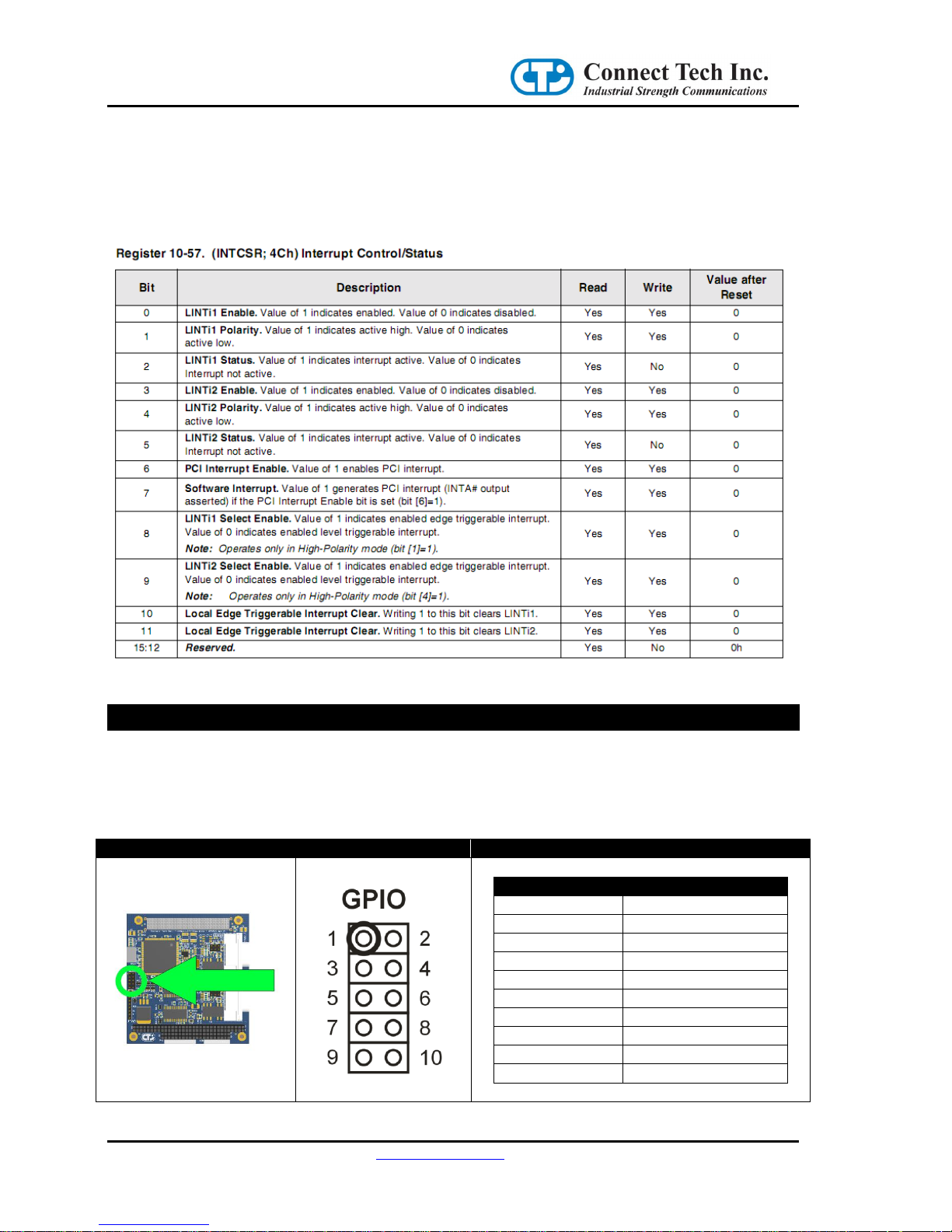
Header Location
Pin Locations
Signal Descriptions
_
Pin Number
Signal
1
GPIO BIT 0
2
GPIO BIT 1
3
GPIO BIT 2
4
GPIO BIT 3
5
GPIO BIT 4
6
GPIO BIT 5
7
GPIO BIT 6
8
GPIO BIT 7
9
+3.3V
10
GND
CAN Controller Interrupts
Each CAN controller is tied to a local interrupt on the PLX9030 which is then forwarded to a single interrupt
on the PCI bus. Access to the PLX9030 interrupt control/status register can be done by accessing the
INTCSR register at offset 4Ch from the PCI base address of the CANpro/104-Plus Opto.
This diagram is taken from the PLX9030 Data Book v1.4.
GPIO Details
GPIO Header
CANpro/104-Plus Opto includes a 10-pin header with 8-bits of 3.3V General Purpose IO. The location and
description of this header can be found below.
CTIM-00052 Revision 0.00 4/23/2009 www.connecttech.com 18
800-426-8979 | 519-836-1291
Page 19

CANpro/104-Plus Opto User Manual
GPIO Control and Addressing
GPIO pins on the CANpro/104-Plus Opto are controlled via the GPIOC register within the PLX 9030. The
register is located at offset 0x54 from the PLX9030 PCI Base Address. The CANpro/104-Plus Opto ships
with all GPIO pins set up as a data output pin by default.
This diagram is taken from the PLX9030 Data Book v1.4.
19 www.connecttech.com CTIM-00052 Revision 0.00 4/23/2009
800-426-8979 | 519-836-1291
Page 20

CANpro/104-Plus Opto User Manual
Specifications
Operating Environment
Storage temperature: -40 C to 125 C
Operating temperature: -40 C to 85 C
Humidity: 95%, non-condensing
Power Requirements
+5 VDC @ 500mA (maximum)
380 mA (minimum)
NOTE:
External power output pins on each CAN port is limited up to
125 mA per port .
PC Bus Interface
PC/104-Plus
Optical/Power Isolation
3kV for each CAN port from the host system and other isolated CAN ports.
Dimensions
Compliant to PC/104-Plus specification 2.2
Connectors/Interface
Standard: 10-pin, right angled header
Optional: DB-9
GPIO
8-bit 3.3V I/O header
CTIM-00052 Revision 0.00 4/23/2009 www.connecttech.com 20
800-426-8979 | 519-836-1291
Page 21

CANpro/104-Plus Opto User Manual
Certification
Certification for CANpro/104-Plus Opto
The CANpro/104-Plus Opto product family is to be included into a device ultimately subject to FCC, DOC/IC,
and CE certification. The customer is responsible for bringing the completed device into compliance prior to
resale.
Connect Tech has designed CANpro/104-Plus Opto with EMI and EMC considerations such as:
Ground and power planes
Controlled slew-rate signals
EMI/EMC reducing PCB layout
21 www.connecttech.com CTIM-00052 Revision 0.00 4/23/2009
800-426-8979 | 519-836-1291
Page 22

CANpro/104-Plus Opto User Manual
Limited Lifetime Warranty
Connect Tech Inc. provides a Lifetime Warranty for all Connect Tech Inc. products. Should this product, in
Connect Tech Inc.'s opinion, fail to be in good working order during the warranty period, Connect Tech Inc.
will, at its option, repair or replace this product at no charge, provided that the product has not been subjected
to abuse, misuse, accident, disaster or non Connect Tech Inc. authorized modification or repair.
You may obtain warranty service by delivering this product to an authorized Connect Tech Inc. business
partner or to Connect Tech Inc. along with proof of purchase. Product returned to Connect Tech Inc. must be
pre-authorized by Connect Tech Inc. with an RMA (Return Material Authorization) number marked on the
outside of the package and sent prepaid, insured and packaged for safe shipment. Connect Tech Inc. will
return this product by prepaid shipment service.
The Connect Tech Inc. lifetime warranty is defined as the serviceable life of the product. This is defined as
the period during which all components are available. Should the product prove to be irreparable, Connect
Tech Inc. reserves the right to substitute an equivalent product if available or to retract lifetime warranty if no
replacement is available.
The above warranty is the only warranty authorized by Connect Tech Inc. Under no circumstances will
Connect Tech Inc. be liable in any way for any damages, including any lost profits, lost savings or other
incidental or consequential damages arising out of the use of, or inability to use, such product.
Customer Support Overview
If you experience difficulties after reading the manual and/or using the product, contact the Connect Tech
reseller from which you purchased the product. In most cases the reseller can help you with product
installation and difficulties.
In the event that the reseller is unable to resolve your problem, our highly qualified support staff can assist
you. Our online Support Center is available 24 hours a day, seven days a week on our website at:
www.connecttech.com/sub/support/support.asp. Please go to the Download Zone or the Knowledge Database
for product manuals, installation guides, device driver software and technical tips. Submit your questions to
our technical support engineers at support@connecttech.com. Our technical support is always free.
Contact Information
Telephone/Facsimile
Technical Support representatives are ready to answer your call Monday through Friday, from 8:30 a.m. to
5:00 p.m. Eastern Standard Time. Our numbers for calls are:
Toll: 800-426-8979 (North America only) | Tel: 519-836-1291 | Fax: 519-836-4878 (online 24 hours)
Email/Internet
You may contact us through the Internet. Our email and URL addresses are:
sales@connecttech.com | support@connecttech.com | www.connecttech.com
Mail/Courier
Connect Tech Inc.
42 Arrow Road
Guelph, Ontario, N1K 1S6, Canada
CTIM-00052 Revision 0.00 4/23/2009 www.connecttech.com 22
800-426-8979 | 519-836-1291
 Loading...