

Page 1
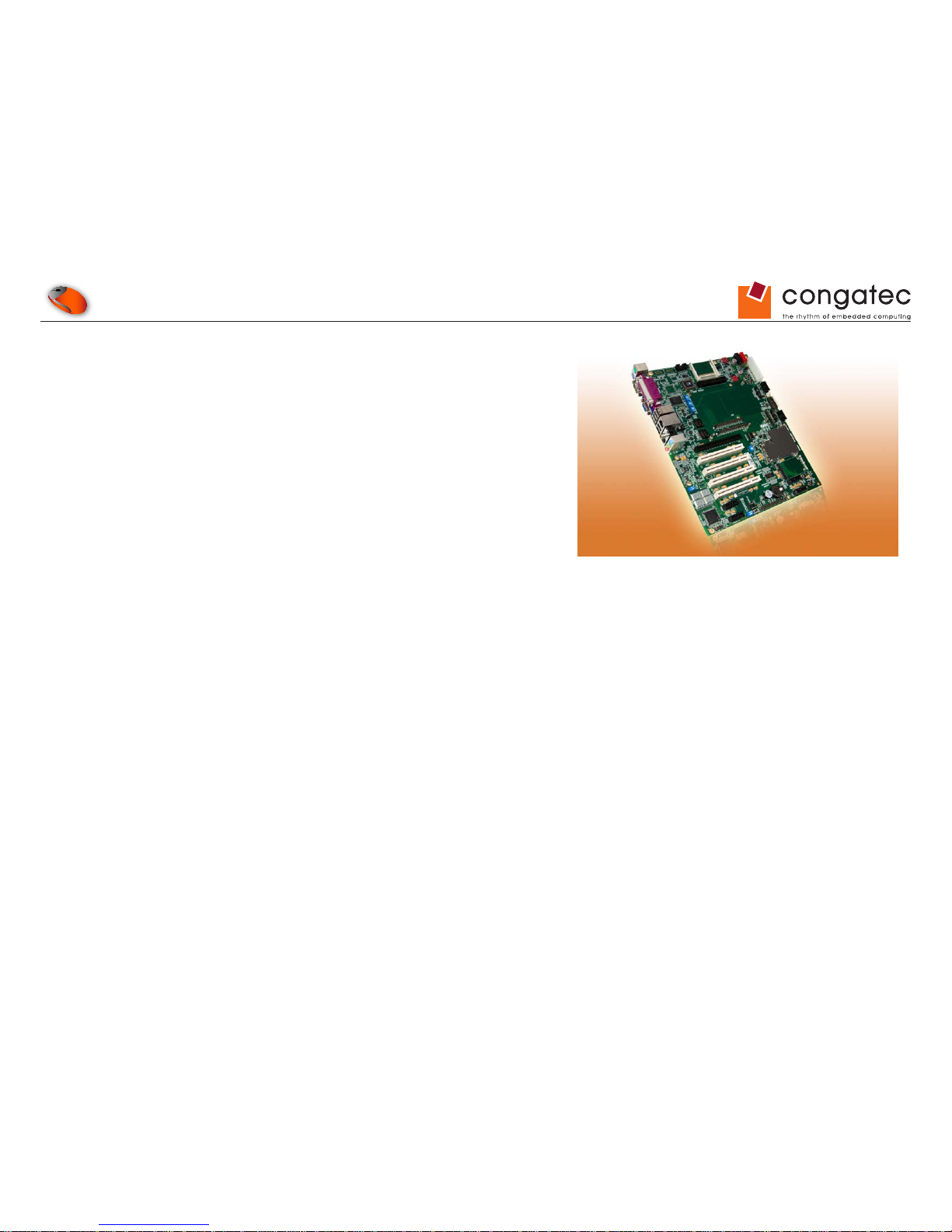
COM Express™ conga-CEVAL
Detailed description of the congatec COM Express™ Type 2 evaluation carrier board
User’s Guide (Rev C.x)
Revision 1.0
Page 2
Copyright © 2012 congatec AG CEVA_c_m10 2/47
Revision History
Revision Date (yyyy.mm.dd) Author Changes
1.0 2013.09.17 AEM • Initial release.
Page 3
Copyright © 2012 congatec AG CEVA_c_m10 3/47
Preface
This user’s guide provides information about the components, features and connectors available on the congatec COM Express™ Type 2
evaluation carrier board.
Disclaimer
The information contained within this user’s guide, including but not limited to any product specication, is subject to change without notice.
congatec AG provides no warranty with regard to this user’s guide or any other information contained herein and hereby expressly disclaims
any implied warranties of merchantability or tness for any particular purpose with regard to any of the foregoing. congatec AG assumes
no liability for any damages incurred directly or indirectly from any technical or typographical errors or omissions contained herein or for
discrepancies between the product and the user’s guide. In no event shall congatec AG be liable for any incidental, consequential, special, or
exemplary damages, whether based on tort, contract or otherwise, arising out of or in connection with this user’s guide or any other information
contained herein or the use thereof.
Intended Audience
This user’s guide is intended for technically qualied personnel. It is not intended for general audiences.
Lead-Free Designs (RoHS)
All congatec AG designs are created from lead‑free components and are completely RoHS compliant.
Electrostatic Sensitive Device
All congatec AG products are electrostatic sensitive devices and are packaged accordingly. Do not open or handle a congatec AG product
except at an electrostatic‑free workstation. Additionally, do not ship or store congatec AG products near strong electrostatic, electromagnetic,
magnetic, or radioactive elds unless the device is contained within its original manufacturer’s packaging. Be aware that failure to comply with
these guidelines will void the congatec AG Limited Warranty.
Page 4
Copyright © 2012 congatec AG CEVA_c_m10 4/47
Symbols
The following symbols are used in this user’s guide:
Warning
Warnings indicate conditions that, if not observed, can cause personal injury.
Caution
Cautions warn the user about how to prevent damage to hardware or loss of data.
Note
Notes call attention to important information that should be observed.
Connector Type
Describes the connector that must be used with the conga‑CEVAL evaluation carrier board, not the connector found on the conga‑CEVAL
evaluation carrier board.
Link to connector layout diagram
This link icon is located in the top left corner of each page. It provides a direct link to the conga‑CEVAL connector layout diagram.
Copyright Notice
Copyright © 2007, congatec AG. All rights reserved. All text, pictures and graphics are protected by copyrights. No copying is permitted without
written permission from congatec AG.
congatec AG has made every attempt to ensure that the information in this document is accurate yet the information contained within is
supplied “as‑is”.
Page 5
Copyright © 2012 congatec AG CEVA_c_m10 5/47
Trademarks
Product names, logos, brands, and other trademarks featured or referred to within this user’s guide, or the congatec website, are the property
of their respective trademark holders. These trademark holders are not afliated with congatec AG, our products, or our website.
Warranty
congatec AG makes no representation, warranty or guaranty, express or implied regarding the products except its standard form of limited
warranty (“Limited Warranty”). congatec AG may in its sole discretion modify its Limited Warranty at any time and from time to time.
Beginning on the date of shipment to its direct customer and continuing for the published warranty period, congatec AG represents that the
products are new and warrants that each product failing to function properly under normal use, due to a defect in materials or workmanship or
due to non conformance to the agreed upon specications, will be repaired or exchanged, at congatec AG’
s option and expense.
Customer will obtain a Return Material Authorization (“RMA”) number from congatec AG prior to returning the non conforming product freight
prepaid. congatec AG will pay for transporting the repaired or exchanged product to the customer.
Repaired, replaced or exchanged product will be warranted for the repair warranty period in effect as of the date the repaired, exchanged or
replaced product is shipped by congatec AG, or the remainder of the original warranty, whichever is longer. This Limited Warranty extends to
congatec AG’s direct customer only and is not assignable or transferable.
Except as set forth in writing in the Limited Warranty, congatec AG makes no performance representations, warranties, or guarantees, either
express or implied, oral or written, with respect to the products, including without limitation any implied warranty (a) of merchantability, (b) of
tness for a particular purpose, or (c) arising from course of performance, course of dealing, or usage of trade.
congatec AG shall in no event be liable to the end user for collateral or consequential damages of any kind. congatec AG shall not otherwise
be liable for loss, damage or expense directly or indirectly arising from the use of the product or from any other cause. The sole and exclusive
remedy against congatec AG, whether a claim sound in contract, warranty, tort or any other legal theory, shall be repair or replacement of the
product only
Certication
congatec AG is certied to DIN EN ISO 9001 standard.
C
E
R
T
I
F
I
C
A
T
I
O
N
I
S
O
9
0
0
1
TM
Page 6
Copyright © 2012 congatec AG CEVA_c_m10 6/47
Technical Support
congatec AG technicians and engineers are committed to providing the best possible technical support for our customers so that our products
can be easily used and implemented. We request that you rst visit our website at www.congatec.com for the latest documentation, utilities and
drivers, which have been made available to assist you. If you still require assistance after visiting our website then contact our technical support
department by email at [email protected]
Terminology
Term Description
PCI Express (PCIe) Peripheral Component Interface Express – next‑generation high speed Serialized I/O bus
PCI Express Lane One PCI Express Lane is a set of 4 signals that contains one differential line for
transmitter and one differential line for receiver. Clocking information is embedded into the
data stream.
x1, x2, x4, x16 x1 refers to one PCI Express Lane of basic bandwidth; x2 to a collection of two PCI Express
Lanes; etc. Also referred to as x1, x2, x4 or x16 link.
ExpressCard A PCMCIA standard built on the latest USB 2.0 and PCI Express buses.
USB Universal Serial Bus
SATA
Serial AT Attachment: serial‑interface standard for hard disks
AC ‘97/HDA Audio CODEC (Coder-Decoder) / High Denition Audio
LPC
Low Pin‑Count Interface: a low speed interface used for peripheral circuits such as Super
I/O controllers, which typically combine legacy‑device support into a single IC.
I²C Bus Inter-Integrated Circuit Bus: is a simple two-wire bus with a software-dened protocol that
was developed to provide the communications link between integrated circuits in a system.
SM Bus System Management Bus: is a popular derivative of the I²C-bus.
SPI Bus Serial Peripheral Bus
GBE Gigabit Ethernet
LVDS
Low‑Voltage Differential Signaling
SDVO Serial Digital Video Out is a proprietary technology introduced by Intel
®
to add additional
video signaling interfaces to a system.
CRT Cathode Ray Tube
DDC Display Data Channel is an I²C bus interface between a display and a graphics adapter.
N.C. Not connected
N.A. Not available
T.B.D. To be determined
Page 7
Copyright © 2012 congatec AG CEVA_c_m10 7/47
Contents
1 COM Express™ Specication Overview ....................................8
1.1 Concept of COM Express™ .......................................................8
1.2 Module Form Factors .................................................................8
1.3 Module Types Overview ...........................................................10
2 Connector Layout .....................................................................12
3 Specications ...........................................................................13
3.1 Mechanical Dimensions ...........................................................13
3.2 Power Supply ...........................................................................13
3.2.1 Status LEDs D1‑D4 ..................................................................15
3.2.2 PWR_OK Signal ......................................................................15
3.2.3 Power‑up Control .....................................................................16
3.2.4 Module Type Detection ............................................................16
3.3 CMOS Battery ..........................................................................17
3.4 Environmental Specications ...................................................17
4 Connector Subsystems Rows A,B,C,D ....................................18
4.1 Connector Pinout Rows A and B ..............................................18
4.1.1 SM Bus ....................................................................................19
4.1.2 I²C Bus .....................................................................................20
4.1.3 SPI Bus ....................................................................................20
4.1.4 HDA Audio ................................................................................21
4.1.4.1 HDA/AC97 Header X49 ...........................................................22
4.1.4.2 Low Pin Count Bus (LPC) ........................................................22
4.1.4.3 LPC Super I/O device ..............................................................23
4.1.4.4 LPC Firmware Hubs .................................................................25
4.1.5 Universal Serial Bus (USB) ......................................................25
4.1.6 LAN 10/100/1000 .....................................................................26
4.1.7 Serial ATA
™ .............................................................................26
4.1.8 VGA ..........................................................................................27
4.1.9 LVDS Flat Panel Interface ........................................................28
4.1.9.1 Flat Panel and Backlight Power Supply ...................................29
4.1.9.2 Flat Panel and Backlight Power Supply Connection ................30
4.1.10 PCI Express x1 Connectors .....................................................31
4.1.11 ExpressCard and PCI Express Mini Card ................................33
4.1.11.1 ExpressCard ............................................................................33
4.1.11.2 PCI Express Mini Card .............................................................34
4.1.12 TV‑Out ......................................................................................36
4.2 Connector Pinout Rows C and D .............................................37
4.2.1 PCI Express Graphics (PEG) ...................................................38
4.2.2 PATA 100 ..................................................................................39
4.2.3 CompactFlash Socket ..............................................................40
4.2.4 PCI BUS ...................................................................................41
5 Additional Features ..................................................................42
5.1 Reset .......................................................................................42
5.2 PC Speaker (Beeper) ...............................................................42
5.3 Debug Display ..........................................................................43
5.4 TPM Physical Presence Pin .....................................................43
5.5 Ground Test Points ..................................................................43
5.6 Fan Connector and Power Conguration .................................44
5.7 SMART Battery Management Module .....................................44
5.8 Feature Connector ...................................................................45
6 Mechanical Drawing conga‑CEVAL ......................................... 46
7 Industry Specications .............................................................47
Page 8
Copyright © 2012 congatec AG CEVA_c_m10 8/47
1 COM Express™ Specication Overview
1.1 Concept of COM Express™
Computer On Module (COM) is off‑the‑shelf technology that has been in the embedded computer industry for years. A Computer On Module
integrates all the core components and standard I/O interfaces of a common PC onto an application specic carrier board. The key advantage
of the COM in the embedded computer industries is that all the highly integrated, high speed components such as CPU, chipsets and memory
are combined on a small module form factor for easy adaptation to different applications across multiple market segments.
COM Express™ modules have standardized form factors and have specied pinouts on the two system connectors that remain the same
regardless of the vendor. The COM Express™ module reects the functional requirements for a wide range of embedded applications. These
functions include, but are not limited to, PCI Express, PCI, Graphics, High Denition Audio, parallel ATA, serial ATA, Gigabit Ethernet and USB
ports. Two ruggedized, shielded connectors provide the carrier board interface and carry all the I/O signals to and from the COM Express™
module.
Carrier board designers can utilize as little or as many of the I/O interfaces as deemed necessary. Therefore the carrier board can provide all
the interface connectors required to attach the system to the application specic peripherals. This versatility allows the designer to create a
dense and optimized package, which results in a more reliable product while simplifying system integration. Most importantly COM Express™
applications are scalable, which means once a product has been created there is the ability to diversify the product range through the use of
different performance class COM Express™ modules. Simply unplug one module and replace it with another ‑ no redesign is necessary.
1.2 Module Form Factors
The COM Express™ specication was developed by the PCI Industrial Computer Manufacturing Group (PICMG) in close collaboration with
many leading companies across the embedded industry in order to nd an implementation solution to handle high speed serial I/Os, processors
and chipsets. COM Express™ 2.0 species three form factors, as well as seven different types of connector pinouts.
The three form factors are Compact, Basic and Extended.
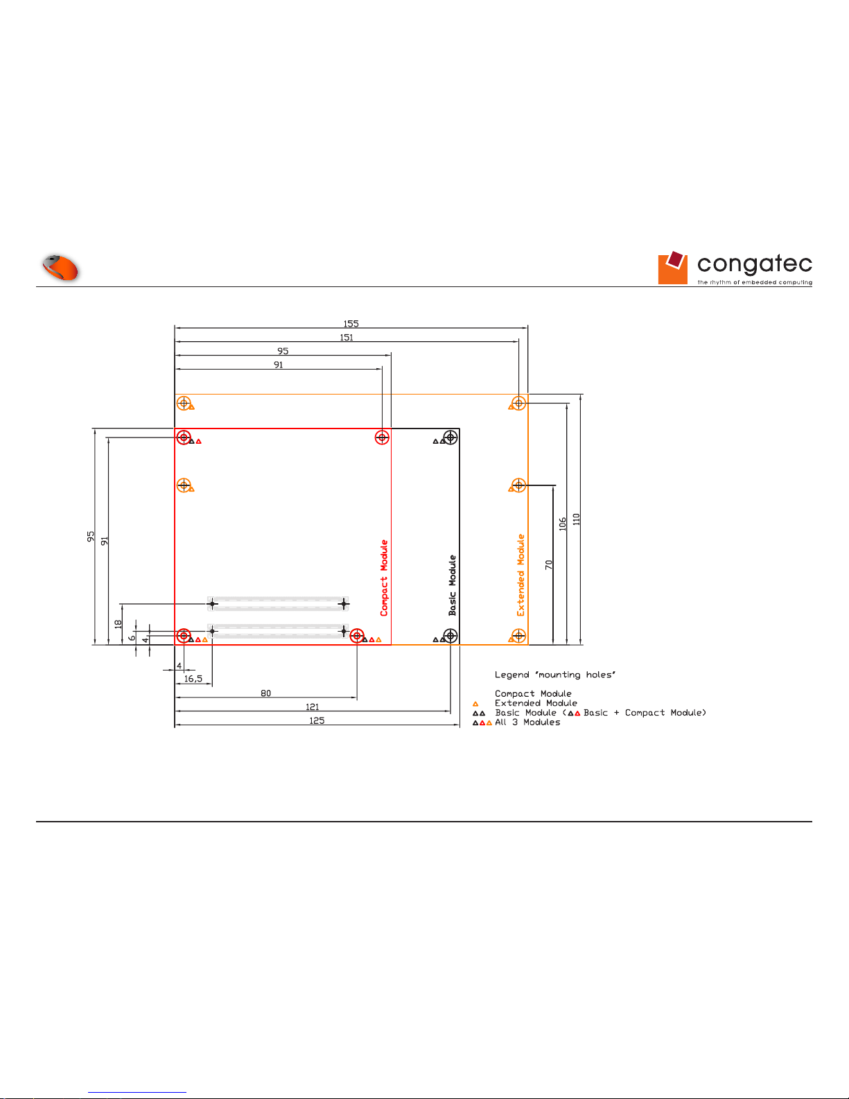
With a form factor of 95x95mm and single (or two stacked) horizontal mount SO‑
DIMM, the Compact module targets space-constrained mobile systems The Basic module footprint is 125mm x 95mm and focuses also on
space‑constrained, low power systems which typically contain one (or two stacked) horizontal mounted SO‑DIMM. The Extended footprint is
slightly larger at 155mm x 110mm and supports up to two full size DIMM (or mini DIMM) modules or two horizontal/vertical mount SO‑DIMMS to
accommodate larger memory congurations for high-performance CPUs, chipsets and multiprocessor systems. The placement of the shielded
220‑pin connectors and the mounting holes are identical between these form factors.
Note
The conga-CEVAL COM Express™ Type 2 evaluation carrier board can host either Compact or Basic form factor CPU modules.
Page 9
Copyright © 2012 congatec AG CEVA_c_m10 9/47
Compact, Basic and Extended Form Factor
Page 10
Copyright © 2012 congatec AG CEVA_c_m10 10/47
1.3 Module Types Overview
The COM Express™ specication 2.0 denes seven different pinout types.
Table 1 COM Express™ Specication 2.0 Pinout Types Denitions
Types Connector
Rows
PCI Express
Lanes
PEG/
SDVO
PCI IDE
Ports
SATA
Ports
LAN
Ports
USB 2.0/
SuperSpeed USB
Display
Interfaces
Type 1 A-B Up to 6 4 1 8/0 VGA, TV Out, LVDS
Type 2 A-B C-D Up to 22 1/2 32 bit 1 4 1 8/0 VGA, TV Out, LVDS, PEG/SDVO
Type 3 A-B C-D Up to 22 1/2 32 bit 4 3 8/0 VGA, TV Out, LVDS, PEG/SDVO
Type 4 A-B C-D Up to 32 1/2 1 4 1 8/0 VGA, TV Out, LVDS, PEG/SDVO
Type 5 A-B C-D Up to 32 1/2 4 3 8/0 VGA, TV Out, LVDS, PEG/SDVO
Type 6 A-B C-D Up to 24
1/‑ 4 1 8/4 3xDDI, PEG, VGA, LVDS
Type 10 A-B Up to 4
‑/1 2 1 8/0 1xDDI
The conga-CEVAL evaluation board uses the Type 2 pin-out denition. This pinout offers the balance between older technology such as PCI
and Parallel ATA while providing the latest technologies including PCI Express, Serial ATA and PCI Express graphics.
The Type 2 pinout denition features the following:
• Dual 220 pin connectors (A-B and C-D)
• 32bit PCI interface
• IDE port (to support legacy ATA devices)
• Up to 22 PCI Express lanes (up to 6 on A-B and up to 16 on C-D)
• 16 of the 22 PCI Express lanes commonly used for PCI Express Graphics
• Option for SDVO (pins shared with PCI Express Graphics)
• Up to 8 USB 2.0 ports
• Up to 4 Serial ATA
• Up to 6 PCI Express lanes (Gen1/Gen2)
• Support pins for up to 2 ExpressCards
Page 11
Copyright © 2012 congatec AG CEVA_c_m10 11/47
• Dual 24‑bit LVDS channels ExpressCards
• Analog VGA
• TV Out
• HDA/AC ‘97 digital audio interface
• Gigabit Ethernet
• LPC interface
• 8 GPIO pins
Page 12
Copyright © 2012 congatec AG CEVA_c_m10 12/47
2 Connector Layout
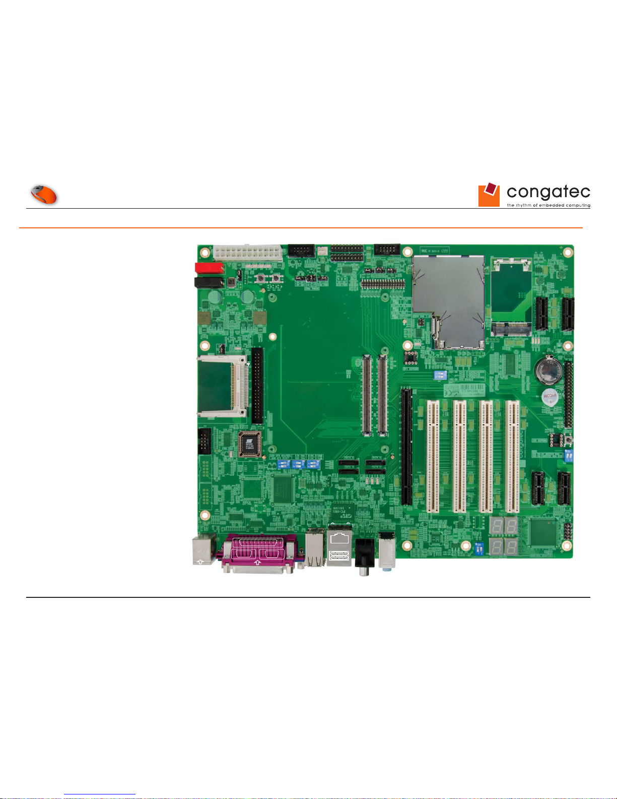
The conga‑CEVAL rev C.x
evaluation board layout
picture on the right features
component description overlay
that includes pinout indicators
as well as name designators.
Select the Adobe ‘Zoom‑
In‑Tool’ and zoom in on a
given component to see the
descriptive text. Hover over the
component and the ‘Zoom‑In‑
Tool’ will change, indicating a
link. Click on the link to navigate
to the area in the document
where the component is
described in detail.
Use the mouse icon in the
top left hand corner of the
destination page to return to
the connector layout picture.
COM1
LPT1
VGA
S1
U16
LAN
USB4
USB5
X47
X39
X1
1-
1
1
2
2
2
9-
9
9
10
10
10
19- 20
X5
X2
D1 10 20 30 40 50 60 70
80
90 100 D110
10
5 15
20 25 30 35 40 45
50
55 60 65
70 75 80
10
5 15
20 25 30 35 40 45
50
55 60 65
70 75 80
AB2
X13
AB1
BB1
LED D21 (WWAN)
LED D22 (WLAN)
LED D21 (WPAN)
A2S3A1
B1
B2
C1 10 20 30 40 50 60 70
80
90 100 C110
B1 10 20 30 40 50 60 70
80
90 100 B110
A1 10 20 30 40 50 60 70
80
90 100 A110
X14
U33
LED D28
X28
X25
X26
X21
Compact Flash Master/Slave
LED D25
M2
X70
Fan Power Cong
X63
PwrGood Cong
X11
X12
X7
M6
X72
X45
X44
M3
TEST PT
TEST PT
TEST PT TEST PT
COMe PWROK
M1
Backlight Power Cong
X67
LCD Power Cong
X66
Backlight Polariy
X69
X16
M40
1
1
1
2
2
5
10152025303334
9 10
19
20
1224
13
5VSBY
LED D1 LED D3 LED D4LED D2
Power Mode
Cong
COM 2
COM 4
optional
COM 3
optional
COM Express A-B Connector
Feature Connector
12V 5V 3.3V
X6
M7
U47
M16
M15
M12
M47
M11
M10
M50
M50
SW1 ON: Enables PC Speaker (beeper)
SW2 ON: Disables HDA
For port selection
M45
X27
EXCD OC
ExpressCard Overcurrent Event
LED D24
X29
X30
X17 X18
X49
X31 X32
X33
XCD1
X34
X41 X42
X35
XAB1
PLCC SOCKET
U27
U25
U31
X54
(Up)
(Down)
X55
X51
L1
L8
ACT LINK
X50
X57
X53
(up)
(down)
C6
C1
V5 V1
V6
V11
V10
V15
13 1
1425
C5
C9
FWH ENA
COMPACT FLASH
+12V
GND
PATA
PATA AC T
Mouse
USB 3
USB 2
USB 1
USB 0
Keyboard
U21
M53 M52 M46
C199 C197
1
9 10
2
4
21
2014
13
5
29
1
9 10
2
1
9 10
2
....
....
....
....
....
....
ATX
SATA 1
TV OUT
Line IN
Line Out
Mic
SATA 3
SATA 0
RESET
SATA 2
PEG
DEBUG DISPLAY
PCI1
PCIe0
PCIe3 PCIe4
PCIe1
HDA/AC97
PCI4
I
2
C EEPROM
Socket
EPI EEPROM
Socket
Express Card
LCD Power
Mini PCI Express
PCI2 PCI3
Pwr On
LCD
FAN
Battery SMB3
I
2
C Digital I/O
Speaker
Battery
Page 13
Copyright © 2012 congatec AG CEVA_c_m10 13/47
3 Specications
3.1 Mechanical Dimensions
294.0 mm x 244.0mm
Height approx. 43mm
3.2 Power Supply
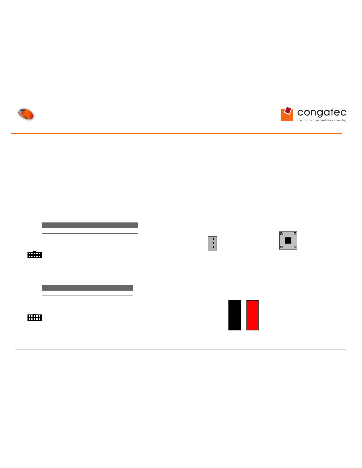
The conga‑CEVAL can be used with standard ATX (Connector X70) power supplies.
When using an ATX power supply, the COM Express™ module starts after the power‑on button M1 is pressed. The ATX power supply can also
be used in AT mode. In this case the module will start after the power switch on the power supply is turned on
Jumper X6 Conguration
1 ‑ 2 ATX Power supply mode (default)
2 ‑ 3 ATX Power supply runs in AT mode
Connector Type
X6: 2.54mm grid jumper.
The conga‑CEVAL can also be used with 12V DC power supply (connector M2 and M7).
Connector Conguration
M7 Ground
M2 +12VDC (11,4 – 12,6V)
Connector Type
4mm diameter plug
1
2
3
Power Mode
Config
(X6)
Pwr On
(M1)
GND
(M7)
+12V
(M2)
Page 14
Copyright © 2012 congatec AG CEVA_c_m10 14/47
The +3.3V and +5V used by some devices on the COM Express™ evaluation carrier board are generated onboard only if 12V DC input (M2,
M7) is used and ATX power connector not plugged in. Otherwise the voltages +3.3V and +5V are delivered by ATX power supply with voltage
regulators disabled.
The voltages used are the +3.3V and +5V. The ‑5V is not available and the ‑12V is not used.
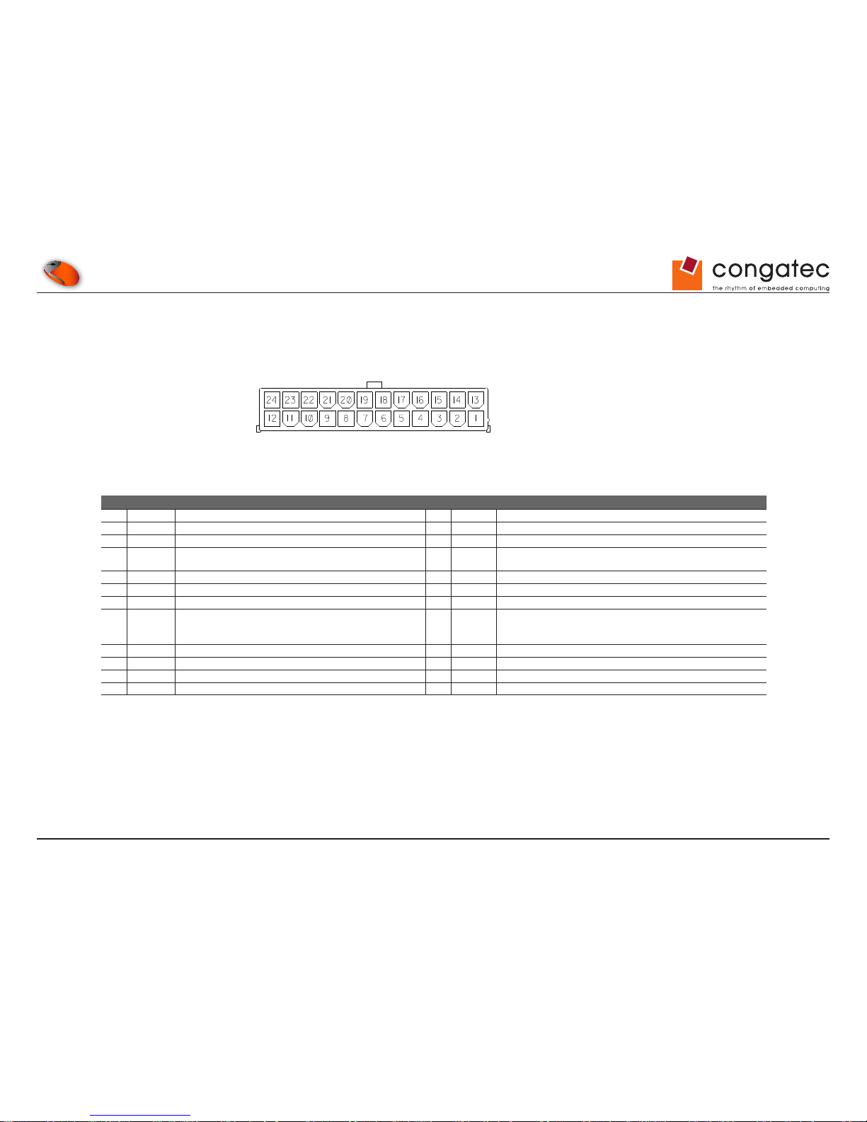
The following table lists the pinout for connector X70.
Table 2 Connector X70 Pinout
Pin Signal Description Pin Signal Description
1 +3.3V Power Supply +3.3VDC 13 +3.3V Power Supply +3.3VDC
2 +3.3V Power Supply +3.3VDC 14
‑12V Power Supply ‑12DC
3 GND Power Ground 15 GND Power Ground
4 +5V Power Supply +5VDC 16 PS_ON# Power Supply On (active low). Short this pin to GND to switch
power supply ON, disconnect from GND to switch OFF.
5 GND Power Ground 17 GND Power Ground
6 +5V Power Supply +5VDC 18 GND Power Ground
7 GND Power Ground 19 GND Power Ground
8 PWR_OK Power Ok: A status signal generated by the power supply
to notify the computer that the DC operating voltages are
within the ranges required for proper computer operation.
20 NC
9 5V_SB Standby Power Supply +5VDC 21 +5V Power Supply +5VDC
10 +12V Power Supply +12DC 22 +5V Power Supply +5VDC
11 +12V Power Supply +12DC 23 +5V Power Supply +5VDC
12 +3.3V Power Supply +3.3VDC 24 GND Power Ground
ATX Power
X70
Page 15
Copyright © 2012 congatec AG CEVA_c_m10 15/47
3.2.1 Status LEDs D1-D4
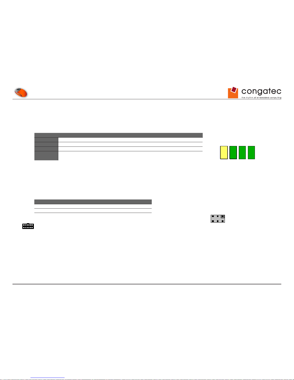
The four status LEDs D1, D2, D3 and D3 indicate different power states of the conga‑CEV AL. The LEDs indicate if the power rail is ON or OFF
even if the power rail is generated by ATX PSU or by onboard voltage regulator. Refer to the following table for detailed information.
Table 3 Power LEDs
LEDs D1-D4 Power state
All Off
No power applied.
D1
Indicates that 12V is present on the baseboard
D2
Indicates that 5V standby is present on the baseboard
D3
Indicates that 5V is present on the baseboard
D4
Indicates that 3.3V is present on the baseboard
3.2.2 PWR_OK Signal
The COM Express™ specication denes the signal PWR_OK, which is a HIGH active input from the main power supply to the module and
indicates whether the power is good.
Jumper X11 on the conga‑CEVAL provides the ability to choose different settings for this signal.
Jumper X11 Conguration
1 ‑ 2 Add 3.3V Pullup with 10K to signal PWR_OK.
3 ‑ 4 Connect PWRGOOD of ATX power supply (default).
5 ‑ 6 Connect PWRGOOD of onboard DCDC regulator.
Connector Type
X11: 2.54 mm grid jumper.
D3 D4D2 D1
LEDs D1-D4
13
24
PWRGOOD Config.
(X11)
5
6
Page 16
Copyright © 2012 congatec AG CEVA_c_m10 16/47
3.2.3 Power-up Control
The Power‑up control switches the ATX power supply on or off. The SUS_S3# activates the ATX power supply by driving the PS_ON# signal.
If DC power input (M2, M7) is used, voltage regulators start after applying +12V.
The native system power‑up support of congatec modules uses the ‘SUS_S3#’ signal to control the ‘PS_ON#’ signal, which switches the ATX
power supply on or off. When using the SUS_S3#’ signal, the COM Express™ module is capable of supporting Suspend to RAM (S3).
When the system goes to Suspend to RAM (S3) or Soft Off (S5), the ‘SUS_S3#’ signal is asserted by the chipset of the module. Through the
use of an inverter, the low active ‘PS_ON#’ signal goes high and switches off the ATX power supply. If the system resides in a power‑down
system state, any system wake‑up event invokes the chipset of the module to deassert the ‘SUS_S3#’ signal. This transitions the system to
Full‑on (S0).
How Suspend to RAM is implemented on a COM Express™ module may differ depending on the module manufacturer. For this reason, it is
recommended that a hardware jumper be implemented on the carrier board in order to provide the ability to choose if the ‘PS_ON#’ signal
should be controlled either by the ‘SUS_S3#’ signal or ‘SUS_S5#’
signal. This is accomplished on earlier conga‑CEVAL revisions through the
use of jumper X63. The conga-CEVAL revision B.0 and later do not implement the jumper X63 (see note below).
Note
On conga-CEVAL revision B.0 and later, the X63 4-pin jumper connector that switches between SUS_S3# and SUS_S5# is not available
because the PS_ON# is driven only by SUS_S3#.
3.2.4 Module Type Detection
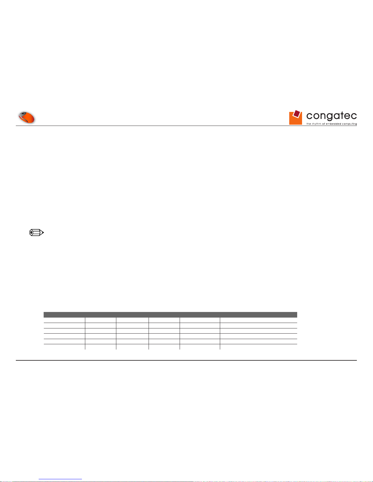
The COM Express™ Specication includes four signals (‘TYPE0#’, ‘TYPE1#’, ‘TYPE2#’ and ‘TYPE10#’) to determine the pinout type of the
module connected to the carrier board. These pins are either left open (NC) or strapped to ground (GND) by the module to encode the pinout
type according to the table below. The ‘TYPE10#’ pin is for dual use. It indicates to the carrier board that a Type 10 module is installed. It also
indicates that a Rev 1.0 or Rev 2.0 module is installed. For more information, refer to the COM Express™ Specication Rev 2.0.
Table 4 Module Type Detection
Module Type Pin TYPE0# Pin TYPE1# Pin TYPE2# Pin TYPE10#
Module Type 1 X (not present) X (not present) X (not present) NC
Module Type 2 NC NC NC NC
Module Type 3 GND NC NC NC No IDE interface
Module Type 4 NC GND NC NC No PCI interface
Module Type 5 GND GND NC NC No IDE, no PCI interface
Module Type 6 NC NC GND NC No IDE, no PCI interface
Page 17
Copyright © 2012 congatec AG CEVA_c_m10 17/47
Module Type Pin TYPE0# Pin TYPE1# Pin TYPE2# Pin TYPE10#
Module Type 10 X (not present) X (not present) X (not present) NC/PD (4.7k)/12V NC indicates Pin‑out Rev. 2.0
PD (4.7k) indicates Pin‑out Type 10
12V indicates Pin‑out Rev.1.0
Note
If an incompatible module pinout type is detected on the conga-CEVAL, an onboard logic will prevent the board from powering up the whole
system by controlling the ‘PS_ON#’ signal of the ATX power supply.
The ‘TYPE[0:2]0#’ signals are not present in Type 1 and Type 10 modules.
3.3 CMOS Battery
The conga‑CEVAL includes a battery that supplies power to the RTC circuit of the COM Express™ CPU module. The battery provides 3V of
power. The specied battery type is CR2032.
Note
To fulll the requirements of the EN60950, the conga-CEVAL incorporates two current-limiting devices (resistor and diode) in the battery power
supply path.
Warning
Danger of explosion if battery is incorrectly replaced. Replace only with the same or equivalent type recommended by the manufacturer.
Dispose used batteries according to the manufacturer’s instructions.
3.4 Environmental Specications
Temperature Operation: 0° to 60°C Storage: ‑20° to +80°C
Humidity Operation: 10% to 90% Storage: 5% to 95%
Note
The above operating temperatures must be strictly adhered to at all times.
Humidity specications are for non-condensing conditions.
Page 18
Copyright © 2012 congatec AG CEVA_c_m10 18/47
4 Connector Subsystems Rows A,B,C,D
4.1 Connector Pinout Rows A and B
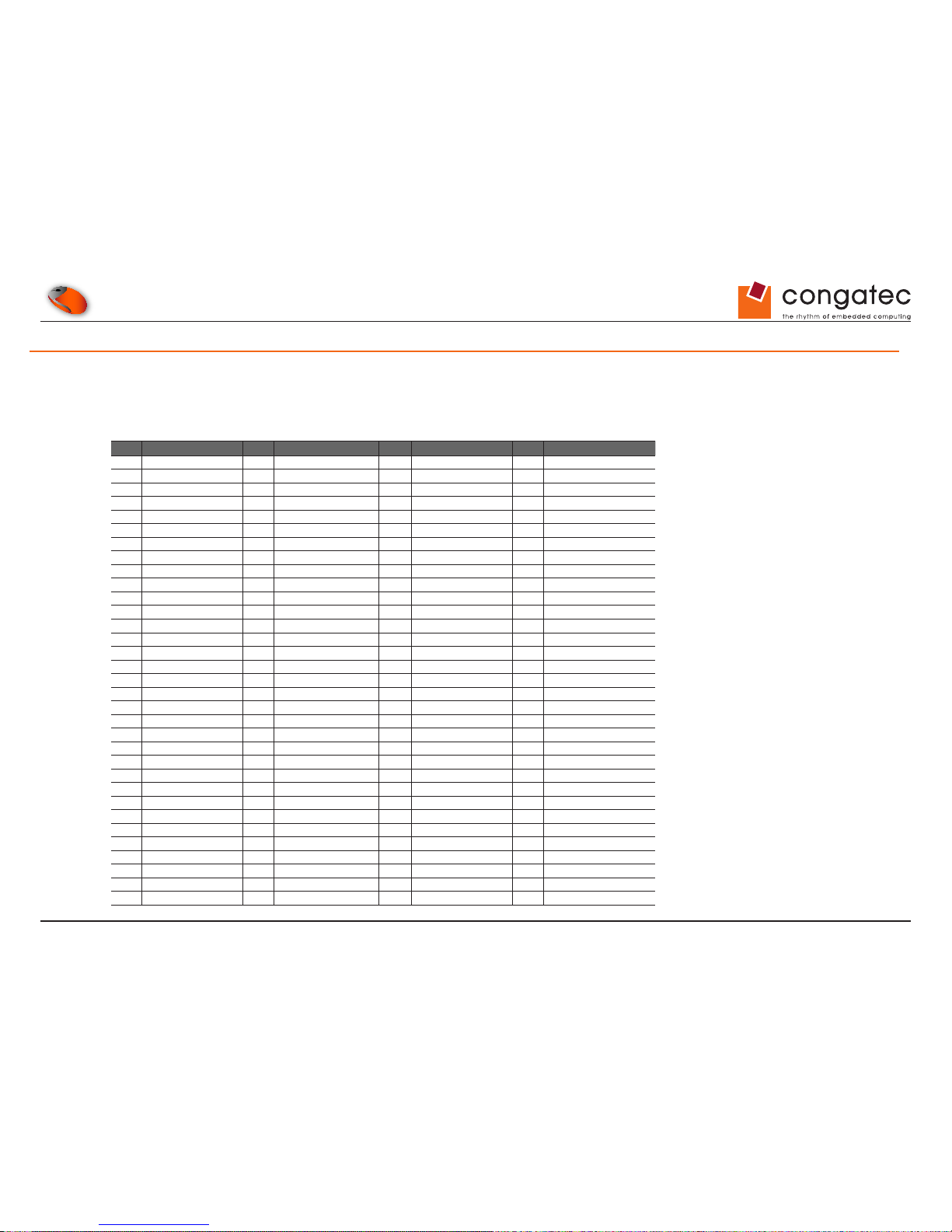
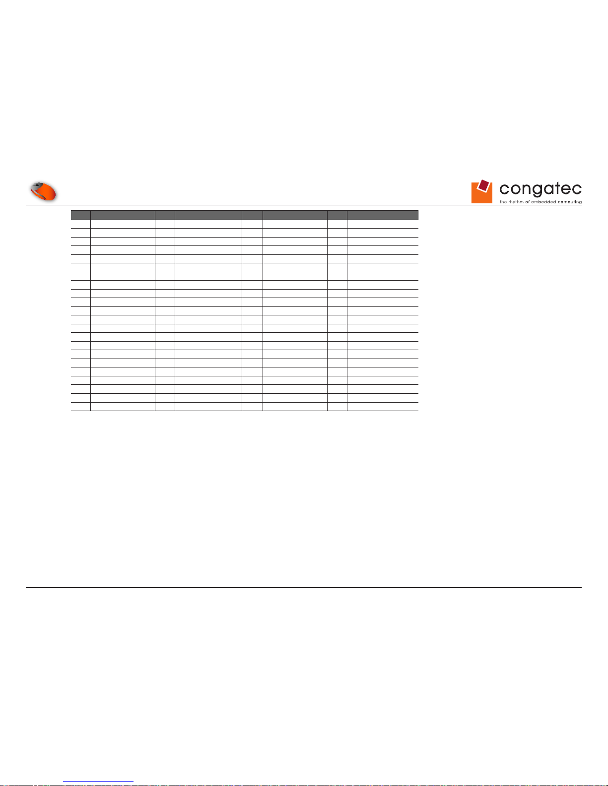
Table 5 Module Type 2 Connector Pinout Rows A and B
Pin Row A Pin Row B Pin Row A Pin Row B
A1 GND (FIXED) B1 GND (FIXED) A56 PCIE_TX4‑ B56 PCIE_RX4‑
A2 GBE0_MDI3- B2 GBE0_ACT# A57 GND B57 GPO2
A3 GBE0_MDI3+ B3 LPC_FRAME# A58 PCIE_TX3+ B58 PCIE_RX3+
A4 GBE0_LINK100# B4 LPC_AD0 A59
PCIE_TX3‑ B59 PCIE_RX3‑
A5 GBE0_LINK1000# B5 LPC_AD1 A60 GND (FIXED) B60 GND (FIXED)
A6 GBE0_MDI2- B6 LPC_AD2 A61 PCIE_TX2+ B61 PCIE_RX2+
A7 GBE0_MDI2+ B7 LPC_AD3 A62
PCIE_TX2‑ B62 PCIE_RX2‑
A8 GBE0_LINK# B8 LPC_DRQ0# A63 GPI1 B63 GPO3
A9 GBE0_MDI1- B9 LPC_DRQ1# A64 PCIE_TX1+ B64 PCIE_RX1+
A10 GBE0_MDI1+ B10 LPC_CLK A65
PCIE_TX1‑ B65 PCIE_RX1‑
A11 GND (FIXED) B11 GND (FIXED) A66 GND B66 WAKE0#
A12 GBE0_MDI0- B12 PWRBTN# A67 GPI2 B67 WAKE1#
A13 GBE0_MDI0+ B13 SMB_CK A68 PCIE_TX0+ B68 PCIE_RX0+
A14 GBE0_CTREF B14 SMB_DAT A69
PCIE_TX0‑ B69 PCIE_RX0‑
A15 SUS_S3# B15 SMB_ALERT# A70 GND (FIXED) B70 GND (FIXED)
A16 SATA0_TX+ B16 SATA1_TX+ A71 LVDS_A0+ B71 LVDS_B0+
A17
SATA0_TX‑ B17 SATA1_TX‑ A72 LVDS_A0‑ B72 LVDS_B0-
A18 SUS_S4# B18 SUS_STAT# A73 LVDS_A1+ B73 LVDS_B1+
A19 SATA0_RX+ B19 SATA1_RX+ A74
LVDS_A1‑ B74 LVDS_B1-
A20
SATA0_RX‑ B20 SATA1_RX‑ A75 LVDS_A2+ B75 LVDS_B2+
A21 GND (FIXED) B21 GND (FIXED) A76
LVDS_A2‑ B76 LVDS_B2-
A22 SATA2_TX+ B22 SATA3_TX+ A77 LVDS_VDD_EN B77 LVDS_B3+
A23
SATA2_TX‑ B23 SATA3_TX‑ A78 LVDS_A3+ B78 LVDS_B3-
A24 SUS_S5# B24 PWR_OK A79
LVDS_A3‑ B79 LVDS_BKLT_EN
A25 SATA2_RX+ B25 SATA3_RX+ A80 GND (FIXED) B80 GND (FIXED)
A26
SATA2_RX‑ B26 SATA3_RX‑ A81 LVDS_A_CK+ B81 LVDS_B_CK+
A27 BATLOW# B27 WDT A82
LVDS_A_CK‑ B82 LVDS_B_CK-
A28 (S)ATA_ACT# B28 AC/HDA_SDIN2 A83 LVDS_I2C_CK B83 LVDS_BKLT_CTRL
A29 AC/HDA_SYNC B29 AC/HDA_SDIN1 A84 LVDS_I2C_DAT B84 VCC_5V_SBY
A30 AC/HDA_RST# B30 AC/HDA_SDIN0 A85 GPI3 B85 VCC_5V_SBY
A31 GND (FIXED) B31 GND (FIXED) A86 KBD_RST# B86 VCC_5V_SBY
A32 AC/HDA_BITCLK B32 SPKR A87 KBD_A20GATE B87 VCC_5V_SBY
A33 AC/HDA_SDOUT B33 I2C_CK A88 PCIE0_CK_REF+ B88 BIOS_DIS1#
Page 19
Copyright © 2012 congatec AG CEVA_c_m10 19/47
Pin Row A Pin Row B Pin Row A Pin Row B
A34 BIOS_DIS0# B34 I2C_DAT A89 PCIE0_CK_REF‑ B89 VGA_RED
A35 THRMTRIP# B35 THRM# A90 GND (FIXED) B90 GND (FIXED)
A36 USB6- B36 USB7- A91 SPI_POWER B91 VGA_GRN
A37 USB6+ B37 USB7+ A92 SPI_MISO B92 VGA_BLU
A38 USB_6_7_OC# B38 USB_4_5_OC# A93 GPO0 B93 VGA_HSYNC
A39 USB4- B39 USB5- A94 SPI_CLK B94 VGA_VSYNC
A40 USB4+ B40 USB5+ A95 SPI_MOSI B95 VGA_I2C_CK
A41 GND (FIXED) B41 GND (FIXED) A96 GND B96 VGA_I2C_DAT
A42 USB2- B42 USB3- A97 TYPE10# B97 SPI_CS#
A43 USB2+ B43 USB3+ A98 RSVD B98 RSVD
A44 USB_2_3_OC# B44 USB_0_1_OC# A99 RSVD B99 RSVD
A45 USB0- B45 USB1- A100 GND (FIXED) B100 GND (FIXED)
A46 USB0+ B46 USB1+ A101 RSVD B101 RSVD
A47 VCC_RTC B47 EXCD1_PERST# A102 RSVD B102 RSVD
A48 EXCD0_PERST# B48 EXCD1_CPPE# A103 RSVD B103 RSVD
A49 EXCD0_CPPE# B49 SYS_RESET# A104 VCC_12V B104 VCC_12V
A50 LPC_SERIRQ B50 CB_RESET# A105 VCC_12V B105 VCC_12V
A51 GND (FIXED) B51 GND (FIXED)
A106 VCC_12V B106 VCC_12V
A52 PCIE_TX5+ B52 PCIE_RX5+ A107 VCC_12V B107 VCC_12V
A53
PCIE_TX5‑ B53 PCIE_RX5‑ A108 VCC_12V B108 VCC_12V
A54 GPI0 B54 GPO1 A109 VCC_12V B109 VCC_12V
A55 PCIE_TX4+ B55 PCIE_RX4+ A110 GND (FIXED) B110 GND (FIXED)
4.1.1 SM Bus
On the COM Express™ module, the System Management Bus (SMB) is powered by the standby power rail in order to have control over the
system during the system states S0‑S5. The devices on the conga‑CEV AL (e.g. PCI Express clock buffer or PCI Express connectors) using the
SMB are normally powered by the 3.3V main power. To avoid current leakage between the main power of the carrier board and the standby
power of the module, a bus switch separates the SMB on the conga-CEVAL carrier board from the SMB of the module.
The SM Bus signals are available on the feature connector (X27) described in section 5.8.
Page 20
Copyright © 2012 congatec AG CEVA_c_m10 20/47
4.1.2 I²C Bus
The I²C signals are available in different locations on the conga‑CEVAL including the feature connector (X27) described in section 5.8 of this
document.
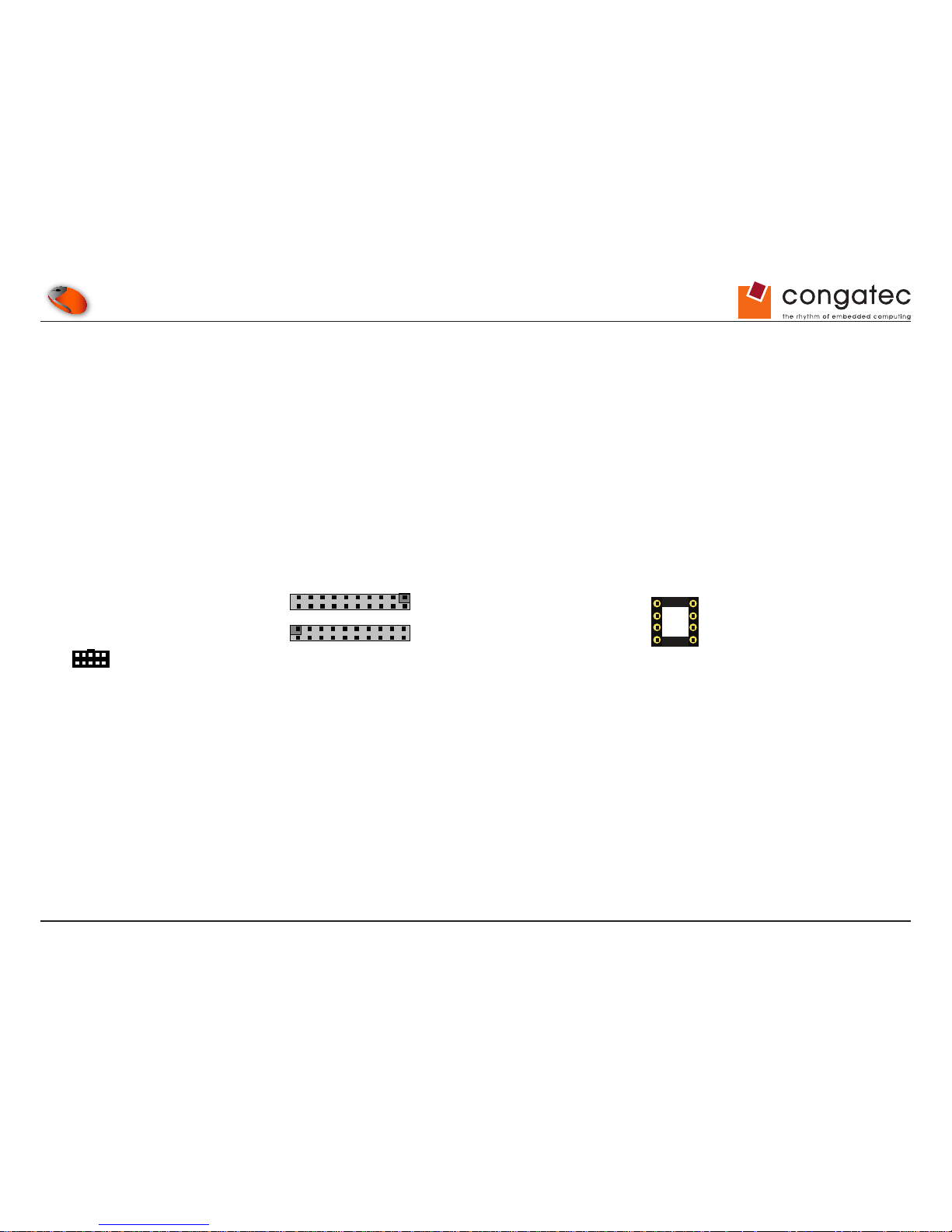
The conga‑CEVAL includes a socket for an I²C EEPROM (U17) that can be used for test purposes during the system development. This 8 pin
DIP socket can be used with different 2‑wire serial EEPROMS (for example 24C04 / 08 / 16 ...) and can be accessed easily by using the I²C
control commands implemented in the congatec CGOS API driver. Refer to the COM Express™ module's user's guide and CGOS manual for
details.
Furthermore, the conga‑CEVAL includes an I²C application implemented by a PCA9555 device from Philips, a 16‑bit I²C I/O port with interrupt.
This device provides 16 bits of general purpose parallel Input/Output (GPIO) expansion for I²C applications. It provides the ability to display and
read different byte congurations via the I²C digital I/O jumper connectors X5 and X12.
Contact the congatec AG support team for more information.
Connector Type
X5/X12: 2.54mm grid header
4.1.3 SPI Bus
The SPI Bus is connected to the SPI BIOS ash that supports off-module BIOS ash boot. The conga-CEVAL revision C1 has onboard an SPI
socket for 8‑lead Small Outline Integrated Circuit (200 mils).
I2C EEPROM
(S3)
1
2
3
4
5
6
7
8
9
10
I²C Digital I/O
X5
X12
11
12
131415
16
17
18
19
20
13245678910111213141516171819
20
Page 21
Copyright © 2012 congatec AG CEVA_c_m10 21/47
4.1.4 HDA Audio
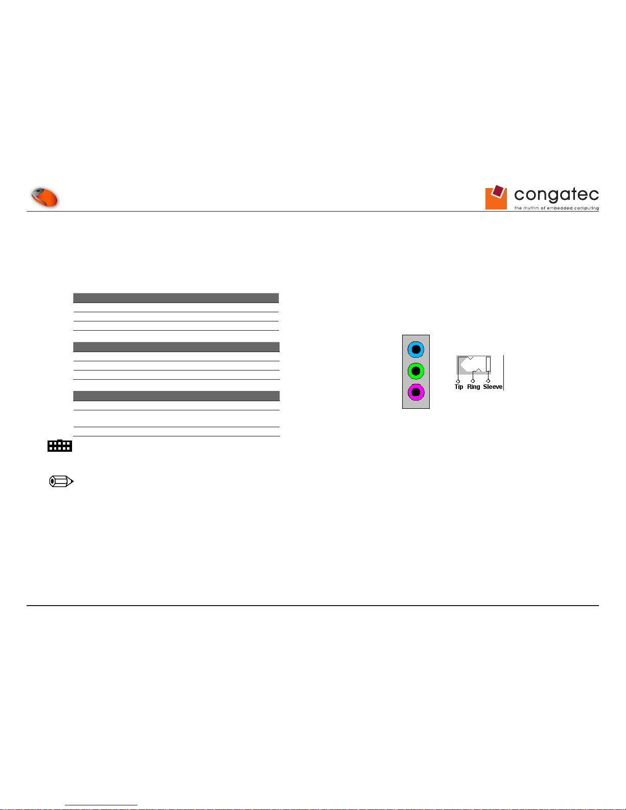
The Realtek ALC888 HDA audio codec is mounted onboard the conga‑CEVAL. The stereo audio output interface of this codec is available
on the X53 connector. The Windows driver for this audio codec can be found on the congatec website at www.congatec.com in the 'Products'
section under 'Accessories'.
The HDA codec can be used either in stereo mode or 5.1 audio mode. The modes can be changed in the audio codec driver.
Stereo Jack 1 Stereo Mode 5.1 Channel Mode
Tip Line Input Left Rear Channel Output Left
Ring Line Input Right Rear Channel Output Right
Sleeve Ground Ground
Stereo Jack 2 Stereo Mode 5.1 Channel Mode
Tip Line Output Left Front Channel Output Left
Ring Line Output Right Front Channel Output Right
Sleeve Ground Ground
Stereo Jack 3 Stereo Mode 5.1 Channel Mode
Tip Microphone Center Output
Ring Not used Low Frequency Effects
Output (Sub Woofer)
Sleeve Ground Ground
Connector Type
X53: triple 3.5mm stereo plug
Note
Mono and stereo microphones can be used on the conga-CEVAL.
SDIN0 and SDIN2 switching are available as assembly option with jumper resistors.
1
2
3
HDA Audio
(X53)
(front view)
Page 22
Copyright © 2012 congatec AG CEVA_c_m10 22/47
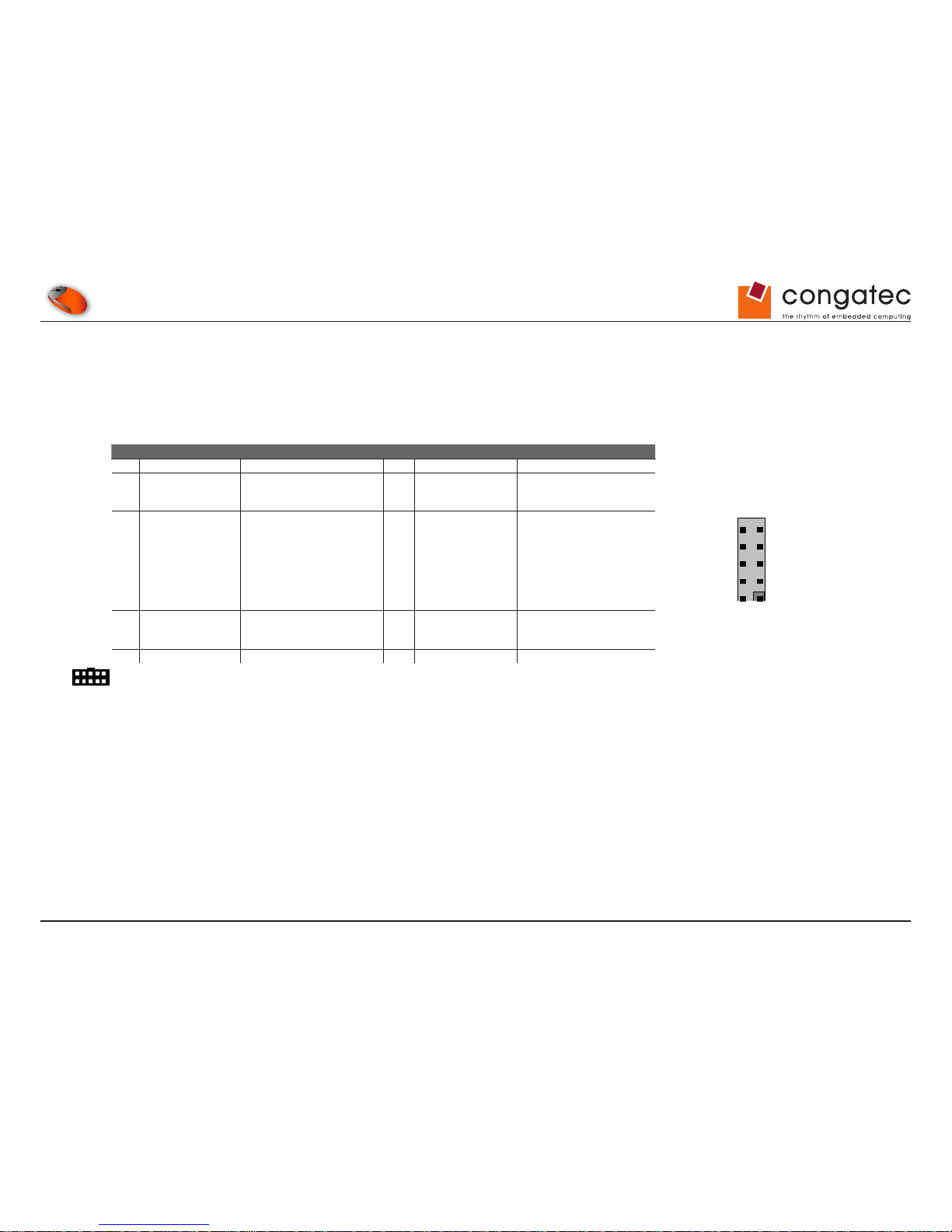
4.1.4.1 HDA/AC97 Header X49
The conga-CEVAL includes a HDA header (X49), which allows the connection of other AC'97/HDA solutions. By attaching a solution to this
connector, the onboard codec switches off and the connected application is then operated. congatec developed a HDA evaluation sound board
that features the VIA VT1708 HDA codec. For more information about this product, contact the congatec AG support team.
The following table describes the pinout of connector X49.
Pin Signal Description Pin Signal Description
1 +12V (750 mA fuse) Power Supply +12VDC 2 +3.3V (750 mA fuse) Power Supply +3.3VDC
3 AC_SYNC/HDA_
SYNC
48kHz xed-rate, sample-
synchronization signal to the
CODEC(s).
4 AC_RST#/HDA_
RST#
Reset output to AC'97/HDA
CODEC, active low.
5 AC_SDIN0/2/HDA_
SDOUT0/2
Serial TDM data inputs from
up to 3 CODECs. SDIN2 is
connected to X49 and SDIN0
is connected to the onboard
HDA codec.
SDIN0 and SDIN2 can be
switched with resistor jumpers
as assembly option.
6 AC_BITCLK/HDA_
SDOUT
12.228 MHz serial data clock
generated by the external
CODEC(s).
7 AC_SDOUT/HDA_
SDOUT
Serial TDM data output to the
CODEC.
8 CODECSET
(Input 3.3V)
Onboard codec disable
input. Pull high to disable
onboard audio codec.
9 GND Power Ground 10 GND Power Ground
Connector Type
X49: 2.54mm grid header.
4.1.4.2 Low Pin Count Bus (LPC)
To use LPC devices, they must be supported by the COM Express™ module's BIOS. Contact the congatec AG support team for more
information about this subject.
13
24
5
6
7
8
9
10
HDA/AC97
(X49)
Page 23
Copyright © 2012 congatec AG CEVA_c_m10 23/47
4.1.4.3 LPC Super I/O device
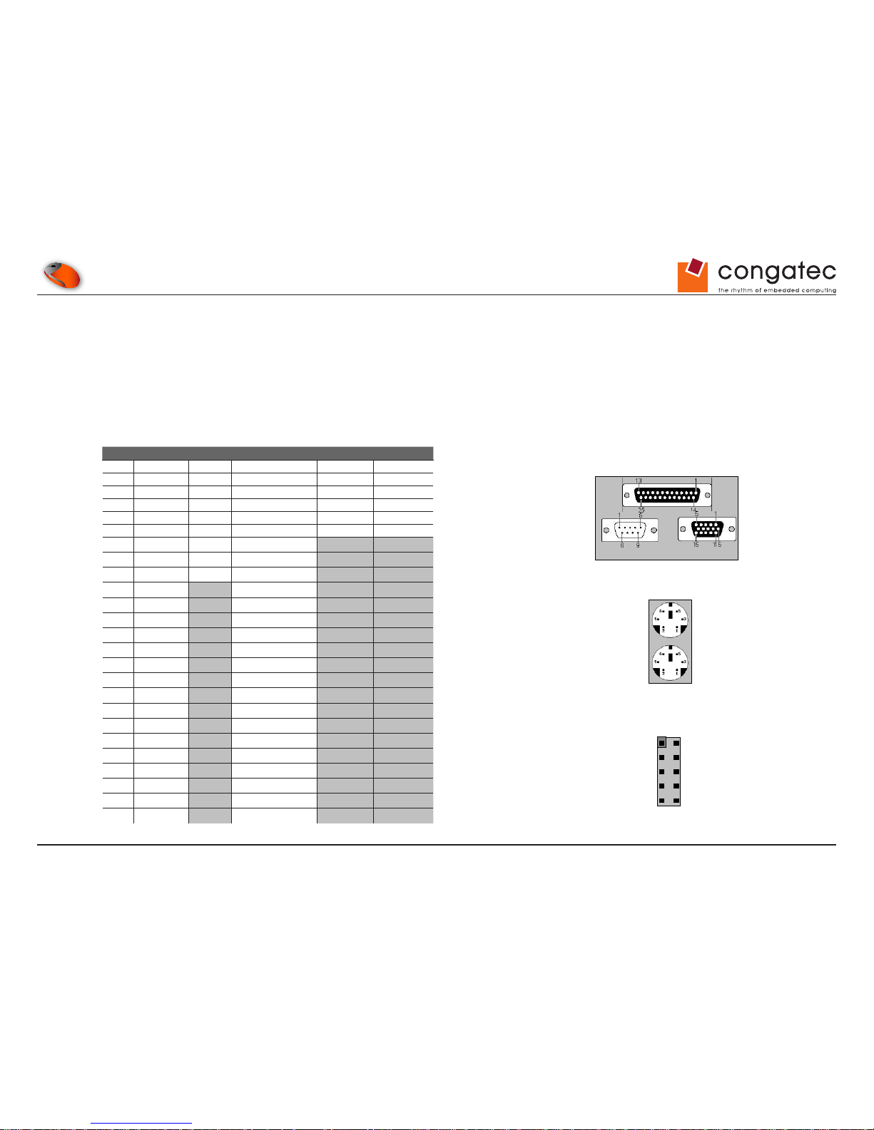
The conga‑CEVAL integrates a Super I/O controller that provides additional interfaces such as PS/2 keyboard and mouse, two serial ports, and
a parallel port. The Winbond W83627HG controller is connected to the LPC Bus of the COM Express™ module and the module must support
these interfaces in order for them to function. Refer to the module's user's guide for information about supported features.
The interfaces provided by this Super I/O controller are available on connectors X28, X38, X54 and X55. Both Serial port COM1 and COM2
are based on RS232 standard.
For the pinout of the mouse, keyboard, COM1, COM2, LPT1 and the Floppy port see the table below.
Pin LPT1 COM1 COM2 Mouse Keyboard
1 STROBE# DCD# DCD# MSDAT KBDAT
2 PD0 RXD DSR N.C. N.C.
3 PD1 TXD RXD GND GND
4 PD2 DTR# RTS# +5V +5V
5 PD3 GND TXD MSCLK KBCLK
6 PD4 DSR CTS# N.C. N.C.
7 PD5 RTS# DTR#
8 PD6 CTS# RI#
9 PD7 RI# GND
10 ACK# +5V (750mA fuse)
11 BUSY
12 PE
13 SEL
14 AUTOFD#
15 ERROR#
16 INIT#
17 SELIN#
18 GND
19 GND
20 GND
21 GND
22 GND
23 GND
24 GND
25 GND
COM1
X55
(front view)
LPT1
VGA
X54
Mouse
Keyboard
1
3
2 4
5
6
7
8
9
10
COM2
(X28)
Page 24
Copyright © 2012 congatec AG CEVA_c_m10 24/47
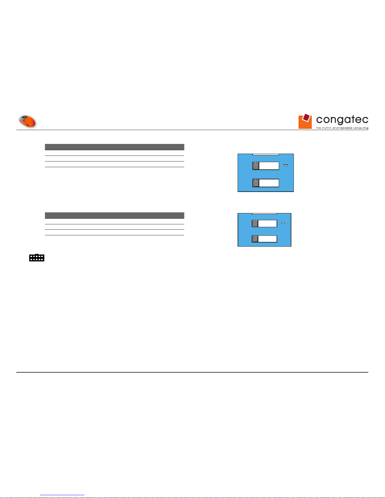
The DIP switch M52 enables or disables the Super I/O and the KB Controller.
DIP Switch M52 Conguration
SW1 On Super I/O Controller Enabled (default)
SW1 Off Super I/O Controller Disabled
SW2 On KB Controller Enabled (default)
SW2 Off KB Controller Disabled
The LPC Super IO address can be selected with the DIP switch M53.
DIP Switch M53 Conguration
SW1 On Super I/O Controller PnP reg. 4Eh
SW1 Off Super I/O Controller PnP reg. 2Eh (default)
SW2 On No defaults for FDC UARTs LPT
SW2 Off Default setting for FDC UARTs LPT
Connector Type
Mouse and Keyboard (X54): 6 pin MINI-DIN female
COM1 (X55): 9 pin, D-SUB male.
LPT1 (X55): 24 pin, D-SUB female. VGA: 15 pin, high density D-SUB female.
COM2 (X28): 10 pin, 2 row 2.54mm grid header.
21
ON
DIP SWITCH
(M52)
21
ON
DIP SWITCH
(M53)
Page 25
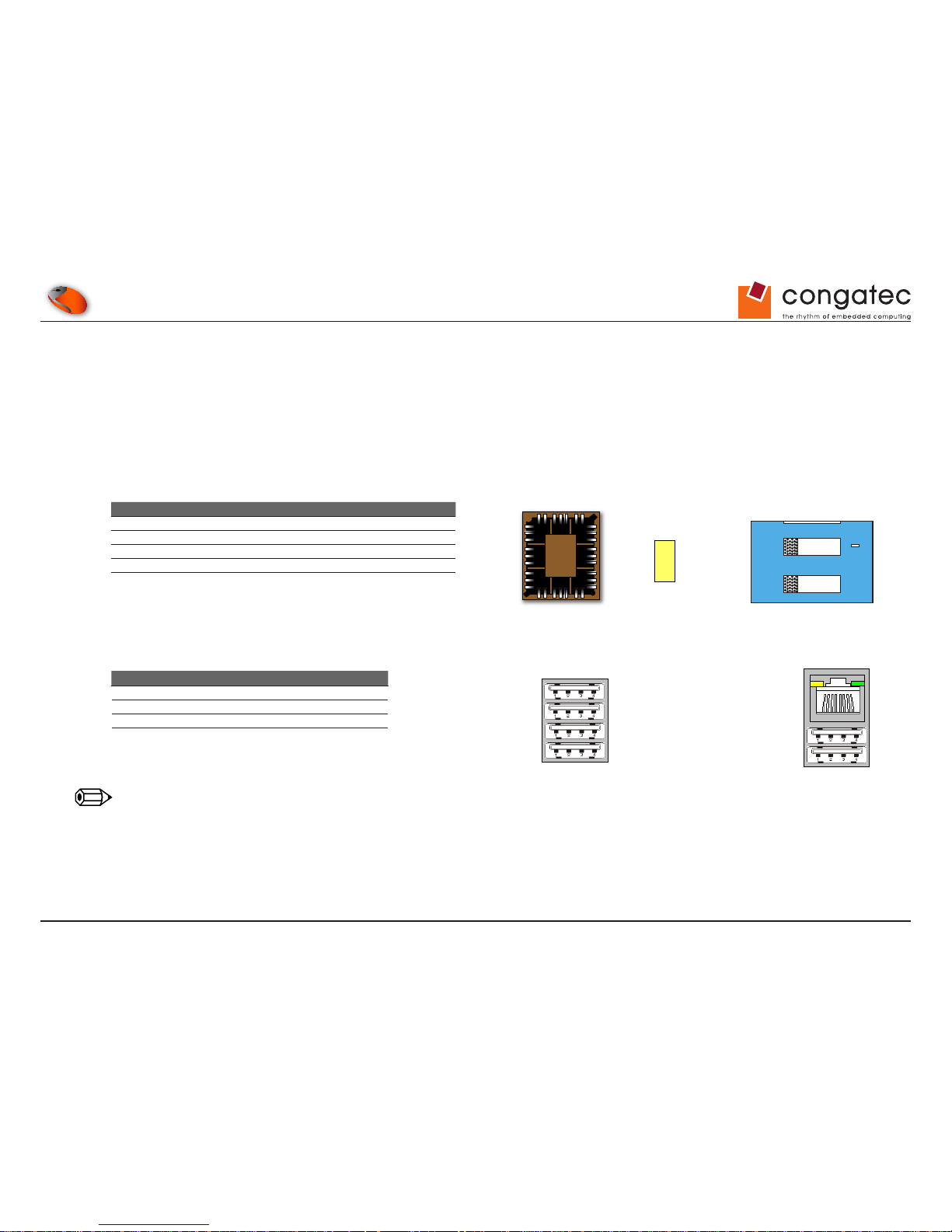
Copyright © 2012 congatec AG CEVA_c_m10 25/47
4.1.4.4 LPC Firmware Hubs
The conga-CEVAL offers the possibility to boot the COM Express™ CPU module with an external BIOS instead of the module’s onboard BIOS.
This can be very useful when a customized BIOS is evaluated.
Onboard the conga-CEVAL is a 32-lead PLCC socket for LPC rmware hub (FWH in socket S1). With the DIP switch M46, you can congure
which rmware hub the COM Express™ CPU module should boot from. When the yellow LED D28 is lit, this indicates the module boots with
the BIOS located on the FWH in socket S1.
The table below shows the different DIP switch settings for M46 necessary to either boot from the carrier board FWH on the conga‑CEVAL or
to boot from the onboard FWH on the COM Express™ CPU module.
DIP Switch M46 Conguration
Switch 1 Switch 2 BIOS Entry / SPI_CS0#
OFF OFF Module FWH or SPI
OFF ON Carrier FWH
ON OFF Carrier SPI CS0#
ON ON Carrier SPI CS1#
4.1.5 Universal Serial Bus (USB)
Pin Signal
1 +5V
2
DATA‑
3 DATA+
4 GND
Note
The USB ports 4 and 5 found on the connector X50 are supplied by suspend power and can be used to test the function "wake-up via USB"
PLCC Socket
S1
D28
21
ON
DIP SWITCH
(M46)
USB Port 3
USB Port 2
USB Port 1
USB Port 0
X51
(front view)
USB Port 4
USB Port 5
X50
(front view)
8 7 6 5 4 3 2 1
Page 26
Copyright © 2012 congatec AG CEVA_c_m10 26/47
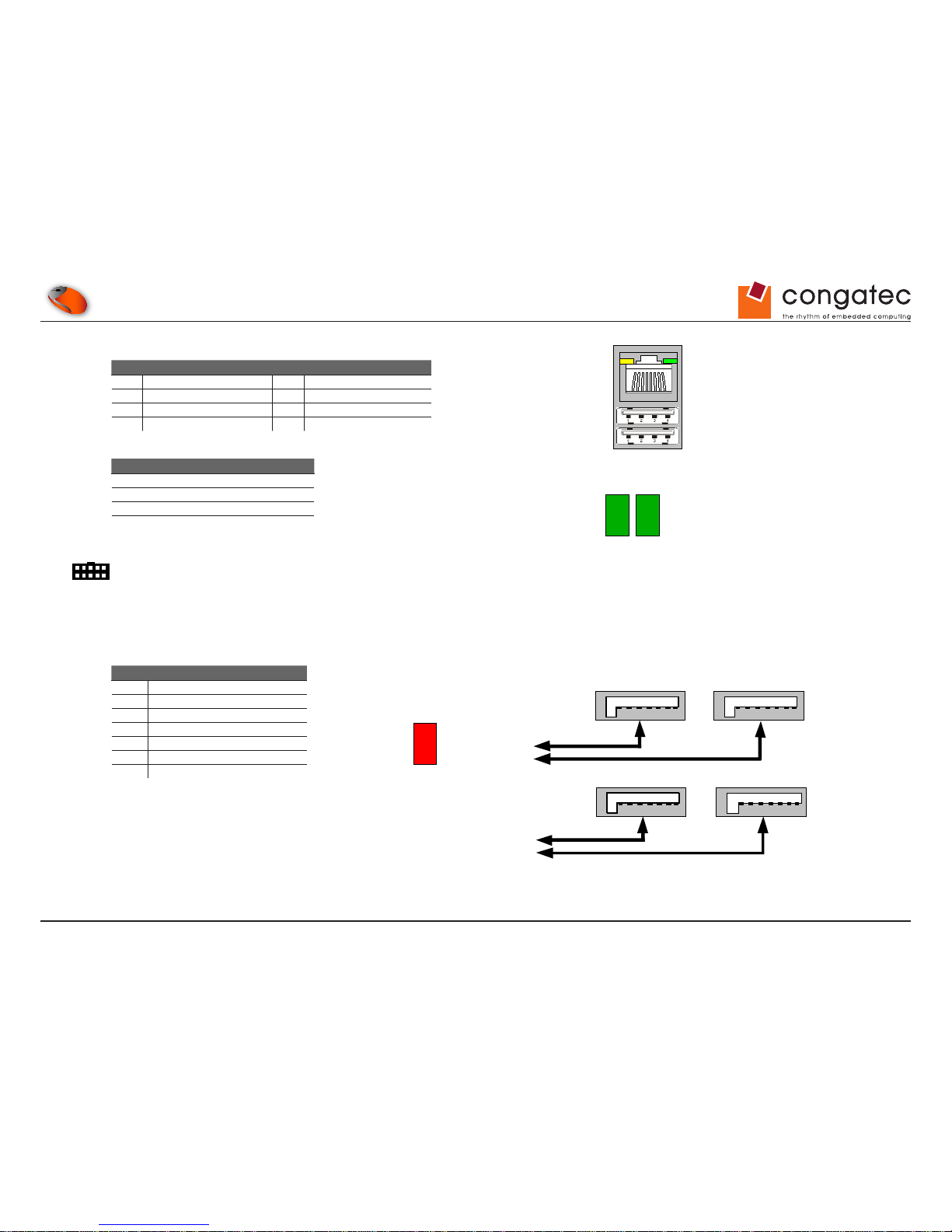
4.1.6 LAN 10/100/1000
Pin Signal Pin Signal
1 MDI[0]+ 2 MDI[0]‑
3 MDI[1]+ 4 MDI[1]‑
5 MDI[2]+ 6 MDI[2]‑
7 MDI[3]+ 8 MDI[3]‑
LEDs Description
Yellow Activity
Green Link
D30 LK100/SLED#
D31 LK1000#
Connector Type
8 pin RJ45 plug
4.1.7 Serial AT A
™
Pin Signal
1 GND
2 TX+
3
TX‑
4 GND
5
RX‑
6 RX+
7 GND
The red LED D29 indicates activity on each SATA interface.
LAN
X50
(front view)
8 7 6 5 4 3 2 1
D30 D31
SATA0 (X35)
SATA2 (X42)
7 6 5 4 3 2 1
SATA1 (X34)
Serial ATA Channel 1
Serial ATA Channel 0
Serial ATA Channel 3
Serial ATA Channel 2
SATA3 (X41)
7 6 5 4 3 2 1
7 6 5 4 3 2 1 7 6 5 4 3 2 1
D29
Page 27
Copyright © 2012 congatec AG CEVA_c_m10 27/47
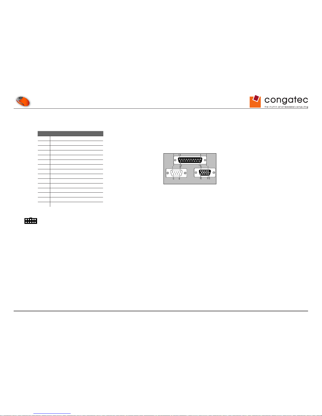
4.1.8 VGA
A CRT monitor can be connected using the X55 connector.
Pin Signal
1 RED
2 GREEN
3 BLUE
4 N.C.
5 GND
6 GND
7 GND
8 GND
9 DDC Power
10 GND
11 N.C.
12 DDC DAT
13 HSYNC
14 VSYNC
15 DDC CLK
Connector Type
VGA (X55): 15 pin, high density DSUB female
COM1
X55
(front view)
LPT1
VGA
Page 28
Copyright © 2012 congatec AG CEVA_c_m10 28/47
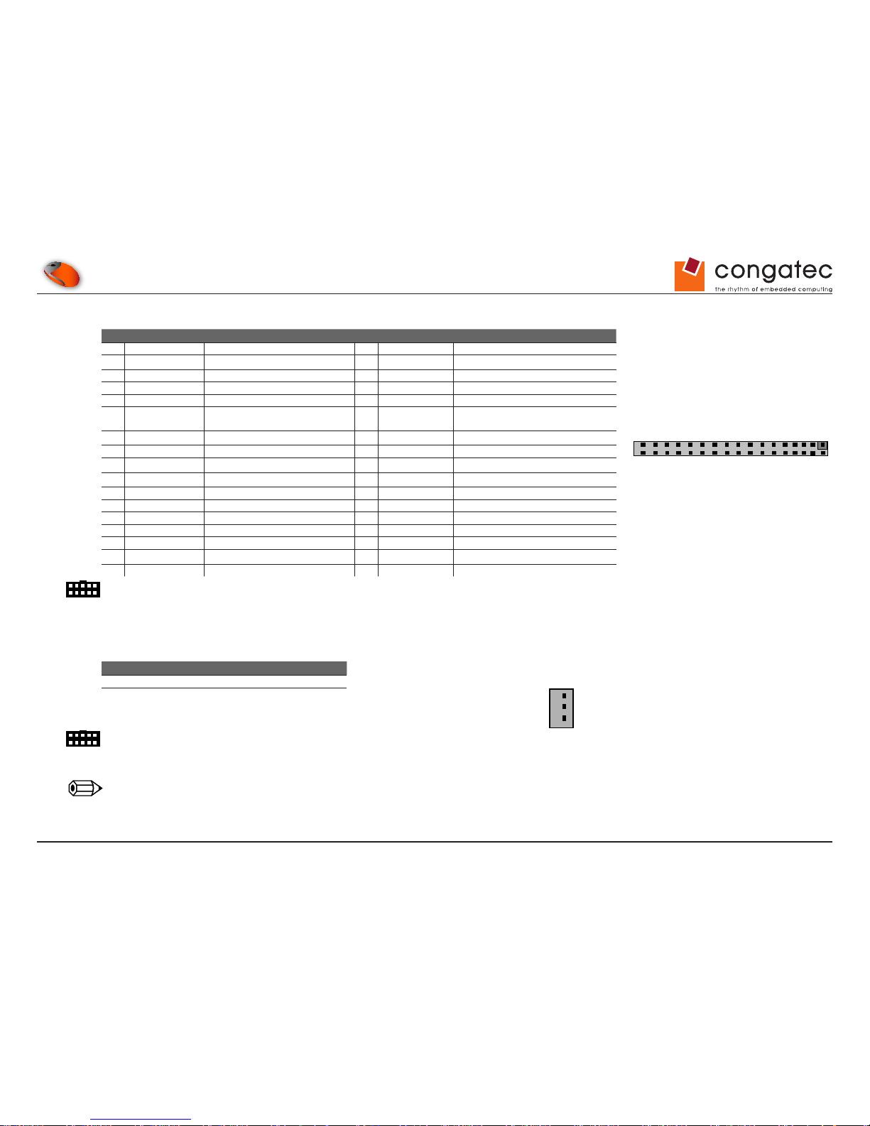
4.1.9 LVDS Flat Panel Interface
Pin LVDS Output Description Pin LVDS Output Description
1 LVDS_I2C_DAT I²C data line for LVDS display use 2 LVDS_I2C_CK I²C clock output for LVDS display use
3 N.C. 4 N.C.
5 GND Power Ground 6
LVDS_A0‑ LVDS Channel A differential pairs
7 LVDS_A0+ LVDS Channel A differential pairs 8 LVDS_VDD_EN LVDS panel power enable
9
LVDS_A1‑ LVDS Channel A differential pairs 10 LVDS_A1+ LVDS Channel A differential pairs
11 LVDS_BKLT_EN LVDS panel backlight enable. (see
jumper X4)
12 LVDS_A2+ LVDS Channel A differential pairs
13
LVDS_A2‑ LVDS Channel A differential pairs 14 N.C.
15
LVDS_A_CK‑ LVDS Channel A differential clock 16 LVDS_A_CK+ LVDS Channel A differential clock
17 N.C. 18 LVDS_A3+ LVDS Channel A differential pairs
19
LVDS_A3‑ LVDS Channel A differential pairs 20 GND
21 LVDS_B0- LVDS Channel B differential pairs 22 LVDS_B0+ LVDS Channel B differential pairs
23 GND Power Ground 24 LVDS_B1- LVDS Channel B differential pairs
25 LVDS_B1+ LVDS Channel B differential pairs 26 GND Power Ground
27 LVDS_B2- LVDS Channel B differential pairs 28 LVDS_B2+ LVDS Channel B differential pairs
29 GND Power Ground 30 LVDS_B_CK+ LVDS Channel B differential clock
31 LVDS_B_CK- LVDS Channel B differential clock 32 N.C.
33 LVDS_B3+ LVDS Channel B differential pairs 34 LVDS_B3- LVDS Channel B differential pairs
Connector Type
X13: 34 pin, 2 row 2mm grid header.
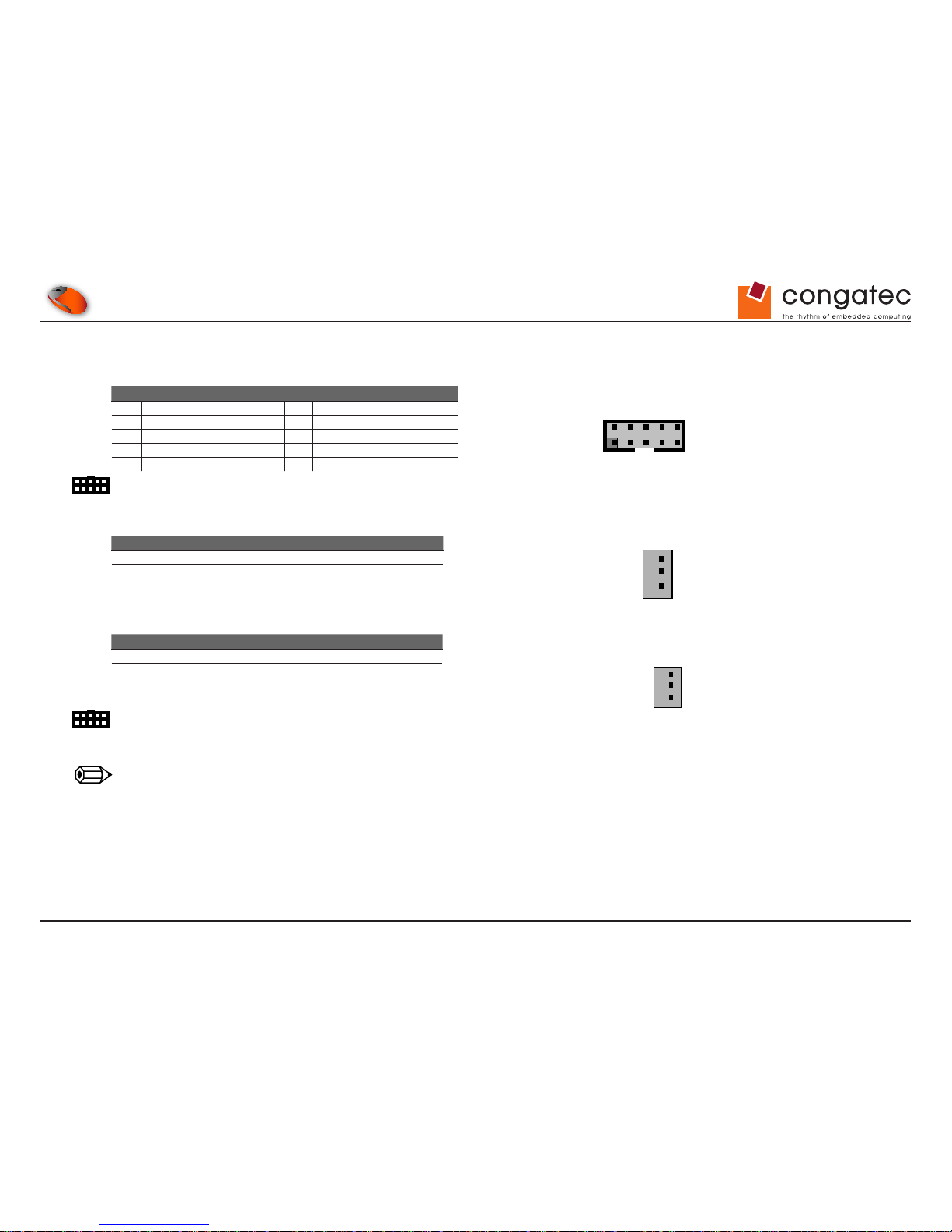
The polarity of the backlight enable signal LVDS_BKLT_EN from the COM Express™ module can be set up using conguration jumper X69.
Jumper X69 Conguration
1 ‑ 2 Backlight enable HIGH active (default)
2 ‑ 3 Backlight enable LOW active (inverted)
Connector Type
X69: 2.54mm grid jumper.
Note
See section 4.1.9.2 “Flat Panel and Backlight Power Supply Connection” for information about connection possibilities for the Backlight Polarity
Cong. jumper X69.
132456789
10
LCD
(X13)
1112131415161718192021222324252627282930313233
34
1
2
3
Backlight Polarity Config
(X69)
Page 29
Copyright © 2012 congatec AG CEVA_c_m10 29/47
4.1.9.1 Flat Panel and Backlight Power Supply
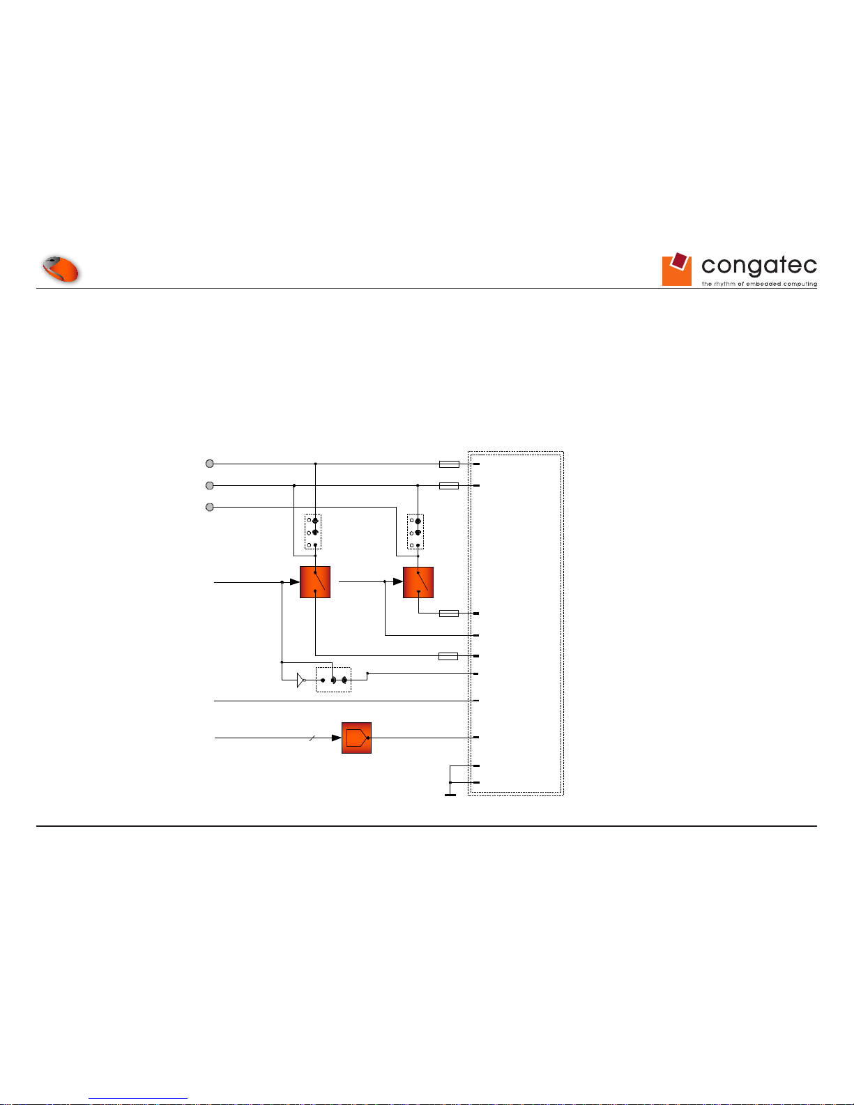
The power supply for at panels and their backlight inverter is available on connector X2.
Pin Signal Pin Signal
1 SW_VDD (1.5A Fuse) 2 SW_BACK (2.0A Fuse)
3 +5V (1.5A Fuse) 4 +12V (2.0A Fuse)
5 DIGON 6 BL_ON
7 BKLT_CTRL_DAC 8 LVDS_BKLT_CTRL_R
9 GND 10 GND
Connector Type
X2: 10 pin, 2 row 2.54 mm grid box header.
Jumper X66 Conguration
1 ‑ 2 5V LCD Voltage (default)
2 ‑ 3 3.3V LCD Voltage
Jumper X8 Conguration
1 ‑ 2 12V Backlight Voltage (default)
2 ‑ 3 5V Backlight Voltage
Connector Type
X66 and X67: 2.54mm grid jumper
Note
See section 4.1.9.2 “Flat Panel and Backlight Power Supply Connection” for information about connection possibilities for the LCD Power X2
connector.
1089765432
1
LCD Power
(X2)
1
2
3
LCD Power Config
(X66)
1
2
3
Backlight Power Config
(X67)
Page 30
Copyright © 2012 congatec AG CEVA_c_m10 30/47
4.1.9.2 Flat Panel and Backlight Power Supply Connection
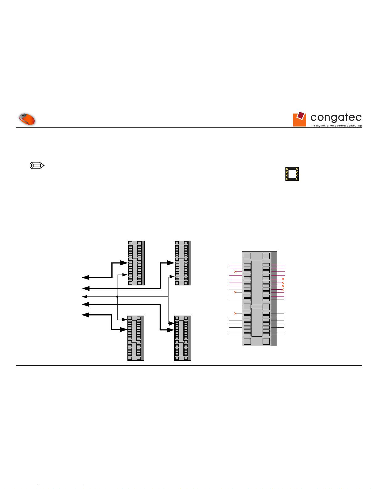
The following diagram shows a typical connection possibility for powering panel/backlight by either the SW_VDD/SW_BACK signals or by
using DIGON/BL_ON for external power switches.
• Signals 1‑10 correspond to signals 1‑10 found on the X2 connector.
• X66, X67 and X69 represent jumpers X66, X67 and X69 found on the conga-CEVAL.
• The conga‑CEVAL carrier board is equipped with a Maxim MAX5362 device referred to in the diagram below as “DAC”. The DAC is a 6‑bit
digital to analog converter..
+3.3V
+5V
+12V
[2] SW_BACK
[6] BL_ON
[1] SW_VDD
[5] DIGON
[8] Backlight Control
from COM Express Module
[7] Backlight Control
from DAC
[9] GND
[10] GND
[4] +12V
[3] +5V
X2
LVDS_VDD_EN
1
2
3
1
2
3
2.0A
1.5A
2.0A
1.5A
X66
X67
2
I2C
DAC
3 2 1
LVDS_BKLT_EN
LVDS_BKLT_CTRL
X69
Page 31
Copyright © 2012 congatec AG CEVA_c_m10 31/47
Flat Panel Conguration Data
The at panel conguration data (EPI extended EDID™ 1.3 le) for most common displays is included in the congatec COM Express™ CPU
module's system BIOS. The customer also has the possibility to store a customized EPI extended EDID™ 1.3 le in a serial EEPROM and then
connect it on the conga‑CEVAL (DIL 8 socket S2).
Note
Supported EEPROMs: 24C02, 24C04 and 24C16 at address A0h.
4.1.10 PCI Express x1 Connectors
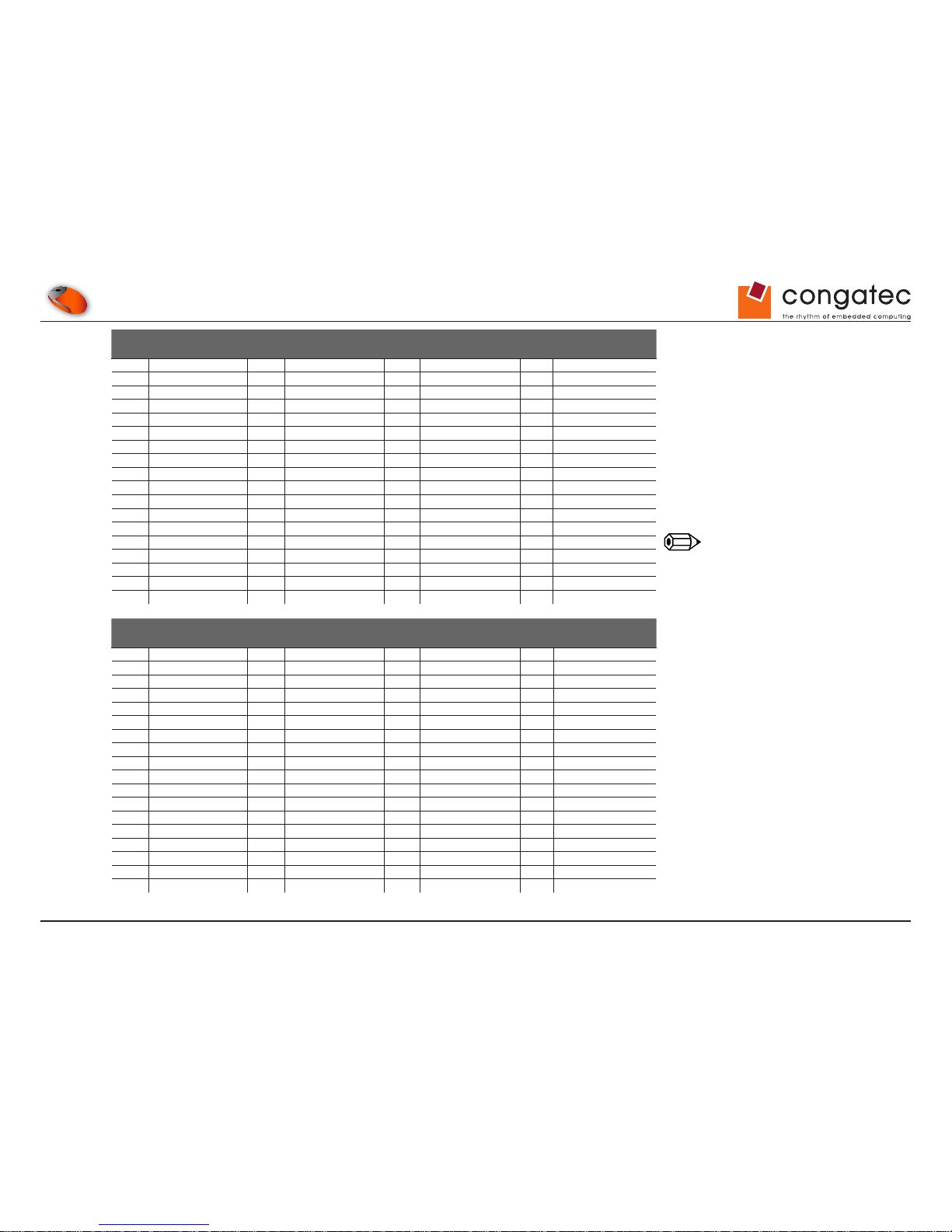
The conga‑CEVAL is equipped with 4 x1 PCI Express Slots. The tables below describe the pinouts for each of these slots.
EPI EEPROM
(S2)
PCIe Slot 0
(X17)
PCIe Slot 1
x1 PCI Express
Connector
(X18)
PCI Express
Lane 0
PCI Express
Lane 3
PCI Express
Lane 4
PCI Express
Lane 1
SM Bus
PCIe Slot 4
(X44)
PCIe Slot 3
(X45)
B2
B1
B4
B3
B6
B5
B8
B7
B10
B9
B13
B12
B14
B15
B17
B16
B18
B11
A1
A5
A2
A9
A8
A7
A6
A14
A13
A12
A10
A18
A17
A16
A15
A11
A4
A3
Page 32
Copyright © 2012 congatec AG CEVA_c_m10 32/47
PCI Express Slot 0/Lane 0 Connector X17 PCI Express Slot 1/Lane 1 Connector X18
Pin Signal Pin Signal Pin Signal Pin Signal
B1 +12V A1 PRSNT#1_S0 B1 +12V A1 PRSNT#1_S1
B2 +12V A2 +12V B2 +12V A2 +12V
B3 N.C. A3 +12V B3 N.C. A3 +12V
B4 GND A4 GND B4 GND A4 GND
B5 SMB_CK A5 N.C. B5 SMB_CK A5 N.C.
B6 SMB_DAT A6 N.C. B6 SMB_DAT A6 N.C.
B7 GND A7 N.C. B7 GND A7 N.C.
B8 +3.3V A8 N.C. B8 +3.3V A8 N.C.
B9 N.C. A9 +3.3V B9 N.C. A9 +3.3V
B10 +3.3V Standby A10 +3.3V B10 +3.3V Standby A10 +3.3V
B11 WAKE0# A11 PCIE_RST# B 11 WAKE0# A11 PCIE_RST#
B12 N.C. A12 GND B12 N.C. A12 GND
B13 GND A13 PCIE_CLKS0+ B13 GND A13 PCIE_CLKS1+
B14 PCIE_TX0+ A14
PCIE_CLKS0‑ B14 PCIE_TX1+ A14 PCIE_CLKS1‑
B15 PCIE_TX0‑ A15 GND B15 PCIE_TX1‑ A15 GND
B16 GND A16 PCIE_RX0+ B16 GND A16 PCIE_RX1+
B17 PRSNT#2_S0 A17
PCIE_RX0‑ B17 PRSNT#2_S1 A17 PCIE_RX1‑
B18 GND A18 GND B18 GND A18 GND
PCI Express Slot 2/Lane 3 Connector X45 PCI Express Slot 3/Lane 4 Connector X44
Pin Signal Pin Signal Pin Signal Pin Signal
B1 +12V A1 PRSNT#1_S2 B1 +12V A1 PRSNT#1_S3
B2 +12V A2 +12V B2 +12V A2 +12V
B3 N.C. A3 +12V B3 N.C. A3 +12V
B4 GND A4 GND B4 GND A4 GND
B5 SMB_CK A5 N.C. B5 SMB_CK A5 N.C.
B6 SMB_DAT A6 N.C. B6 SMB_DAT A6 N.C.
B7 GND A7 N.C. B7 GND A7 N.C.
B8 +3.3V A8 N.C. B8 +3.3V A8 N.C.
B9 N.C. A9 +3.3V B9 N.C. A9 +3.3V
B10 +3.3V Standby A10 +3.3V B10 +3.3V Standby A10 +3.3V
B11 WAKE0# A11 PCIE_RST# B 11 WAKE0# A11 PCIE_RST#
B12 N.C. A12 GND B12 N.C. A12 GND
B13 GND A13 PCIE_CLKS2+ B13 GND A13 PCIE_CLKS3+
B14 PCIE_TX3+ A14
PCIE_CLKS2‑ B14 PCIE_TX4+ A14 PCIE_CLKS3‑
B15 PCIE_TX3‑ A15 GND B15 PCIE_TX4‑ A15 GND
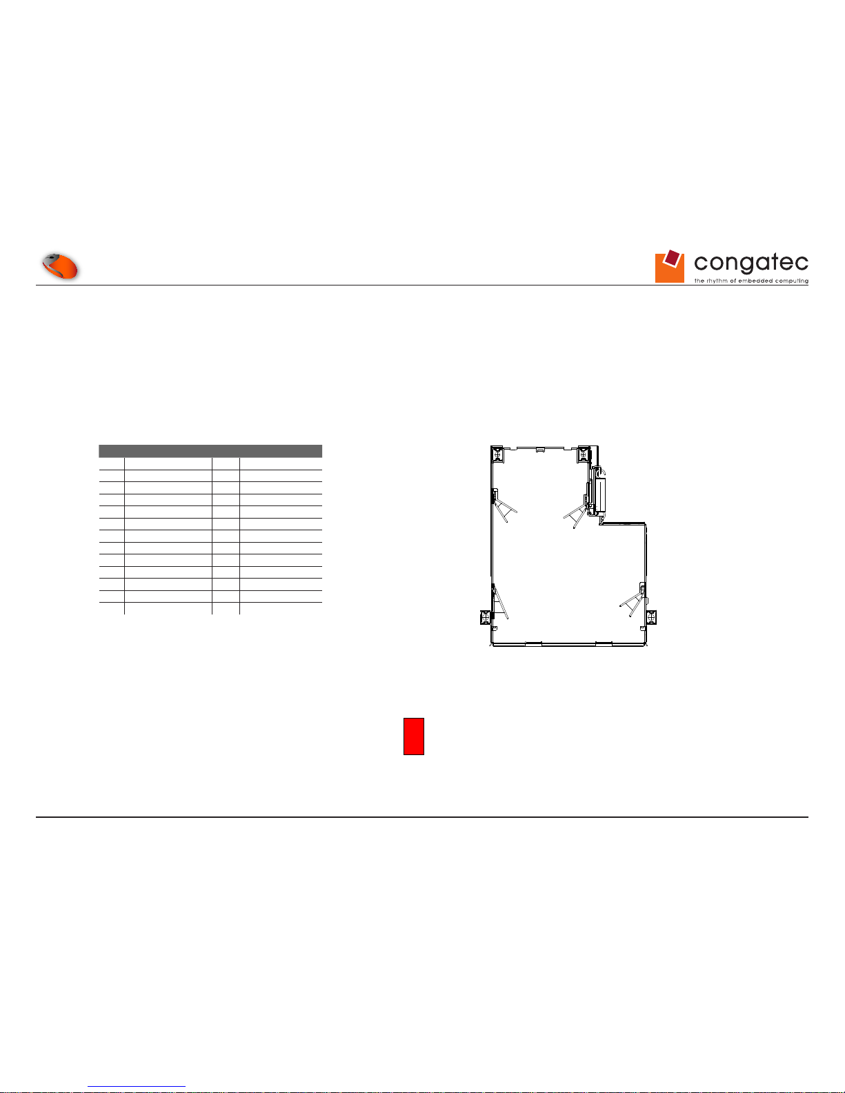
B16 GND A16 PCIE_RX3+ B16 GND A16 PCIE_RX4+
B17 PRSNT#2_S2 A17
PCIE_RX3‑ B17 PRSNT#2_S3 A17 PCIE_RX4‑
B18 GND A18 GND B18 GND A18 GND
The JTAG pins are not connected
on the 4 PCI Express connectors
PCIe0 to PCIe3.
Note
Page 33
Copyright © 2012 congatec AG CEVA_c_m10 33/47
4.1.11 ExpressCard and PCI Express Mini Card
4.1.11.1 ExpressCard
The conga‑CEVAL is equipped with an ExpressCard slot (connector X16). ExpressCard is a small, modular add‑in card designed to replace
common PCMCIA and PC Cards. It takes advantage of the scalable, high-bandwidth serial PCI Express and USB 2.0 interfaces to provide
much higher data rates. COM Express™ modules offer support for up to two ExpressCard slots. More information about the ExpressCard
Standard can be found at http://www.expresscard.org.
The following table lists the default pinout of the ExpressCard slot. It utilizes USB port 6 and PCI Express lane 2 by default.
Pin Signal Pin Signal
1 GND 14 +3.3V
2 USB6- 15 +3.3V
3 USB6+ 16 CLKREQ#
4 CPUSB# 17 EXCD0_CPPE#
5 RSVD 18
PCIE_CLKC0‑
6 RSVD 19 PCIE_CLKC0+
7 SMB_CK 20 GND
8 SMB_DAT 21
PCIE_RX2‑
9 +1.5V 22 PCIE_RX2+
10 +1.5V 23 GND
11 WAKE0# 24
PCIE_TX2‑
12 +3.3V Standby 25 PCIE_TX2+
13 EXCD0_PERST# 26 GND
LED D24 is a red LED that indicates an 'Overcurrent Event' has occurred in the ExpressCard slot.
D24
Page 34
Copyright © 2012 congatec AG CEVA_c_m10 34/47
4.1.11.2 PCI Express Mini Card
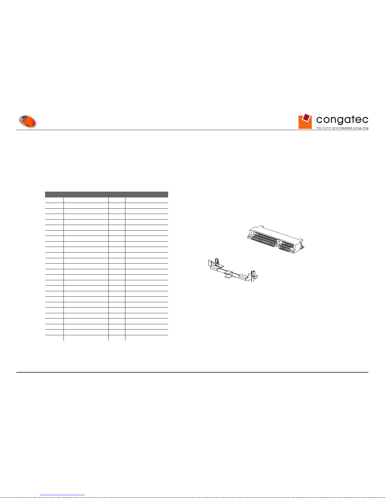
The conga‑CEVAL is equipped with a PCI Express Mini Card socket (M40). PCI Express Mini Card is a unique small size form factor optimized
for mobile computing platforms equipped with communication applications such as Wireless LAN. The small footprint connector can be
implemented on carrier board designs providing the ability to insert different removable PCI Express Mini Cards. Using this approach gives the
exibility to mount an upgradable, standardized PCI Express Mini Card device to the carrier board without additional redesign cost. The PCI
Express Mini Card uses USB port 7 and PCI Express lane 5 by default.
The following table lists the default pinout of the PCI Express Mini Card.
Pin Signal Pin Signal
1 WAKE0# 2 +3.3V
3 RSVD 4 GND
5 RSVD 6 +1.5V
7 CLKREQ# 8 N.C.
9 GND 10 N.C.
11
PCIE_CLKC1‑ 12 N.C.
13 PCIE_CLKC1+ 14 N.C.
15 GND 16 N.C.
17 RSVD 18 GND
19 RSVD 20 RSVD
21 GND 22 EXCD1_PERST#
23
PCIE_RX5‑ 24 +3.3V Standby
25 PCIE_RX5+ 26 GND
27 GND 28 +1.5V
29 GND 30 SMB_CK
31
PCIE_TX5‑ 32 SMB_DAT
33 PCIE_TX5+ 34 GND
35 GND 36 USB7-
37 RSVD 38 USB7+
39 RSVD 40 GND
41 RSVD 42 LED_WWAN#
43 RSVD 44 LED_WLAN#
45 RSVD 46 LED_WPAN#
47 RSVD 48 +1.5V
49 RSVD 50 GND
51 RSVD 52 +3.3V
Page 35
Copyright © 2012 congatec AG CEVA_c_m10 35/47
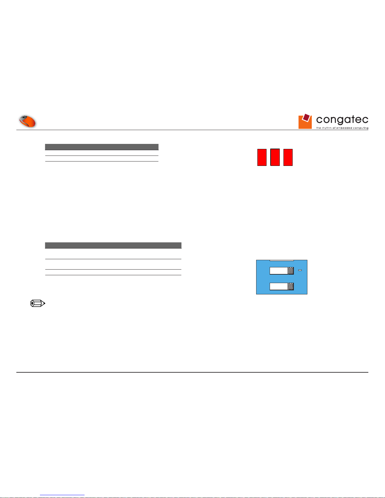
The PCI Mini Card socket has three different red LEDs to indicate the presence of certain area network types. They are as follows:
LED Indicates
21 Wireless Wide Area Network
22 Wireless Local Area Network
23 Wireless Personal Area Network
DIP Switch M47
DIP switch M47 provides the ability to switch between using different PCI Express lanes for the ExpressCard slot and PCI Express Mini Card
socket. This is necessary because some congatec COM Express™ modules have onboard devices attached to PCI Express lane 5. The
default conguration is that the ExpressCard slot uses PCI Express lane 2 and the PCI Express Mini Card socket uses PCI Express lane 5.
In certain cases, it is necessary to use this DIP switch. For instance when dealing with some congatec COM Express™ modules that support
onboard Gigabit Ethernet implemented with PCI Express lane 5. This means that PCI Express lane 5 is not available externally. If the PCI
Express Mini Card socket must be used as well, then it is necessary to congure it to use PCI Express lane 2 instead of the default conguration,
which is PCI Express lane 5. Jumper X62 provides the ability to do this.
DIP Swith M47 Conguration
Switch 1 ON PCIe lane 2 ExpressCard (default)
PCIe lane 5 PCI Express Mini Card (default)
Switch 1 OFF PCIe lane 5 ExpressCard
PCIe lane 2 PCI Express Mini Card
Switch 2 ON PEG port enabled (default)
Switch 2 OFF PEG port disabled
Note
In order to use both the ExpressCard slot and PCI Express Mini Card socket at the same time, PCI Express Lane 2 and 5 must be available.
D21 D22 D23
21
ON
DIP SWITCH
(M47)
Page 36
Copyright © 2012 congatec AG CEVA_c_m10 36/47
4.1.12 TV-Out
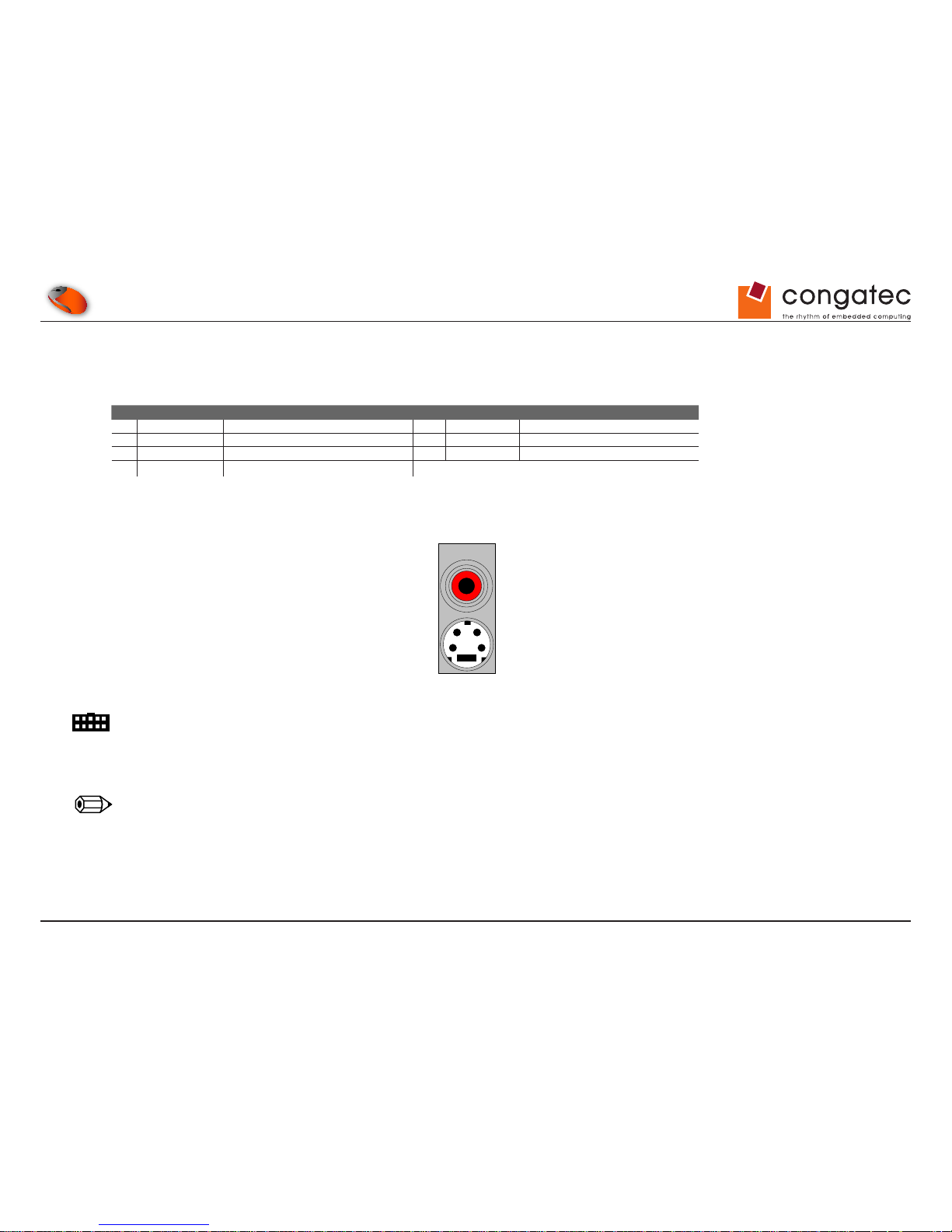
The conga‑CEVAL provides TV‑Out connectors for S‑Video and Composite Video via connector X57. The S‑Video connector can be used with
a standard 4 pin SVIDEO cable whereas the Composite Video requires a coax cable with a RCA jack on each end.
Pin Signal Description Pin Signal Description
1 Chrominance (C) S‑Video Chrominance Analog Signal (C) 2 Luminance (Y) S‑Video Luminance Analog Signal (Y)
3 GND (C) Analog Ground for Chrominance (C) 4 GND (Y) Analog Ground Luminance (Y)
5 GND Analog Ground 6 GND Analog Ground
7 Composite Composite Video Output
Connector Type
X57: Composite Video: Coax cable with RCA jacks on each end
S-VIDEO: 4 pin MINI-DIN female
Note
The conga-CEVAL rev C.1 does not support Composite Video Output by default because this pin is shared with SPI_CS# signal. To support
this output on revision C.1, a simple hardware change is required.
6 7
43
1 2
5
TV-Out
(X57)
(front view)
Page 37
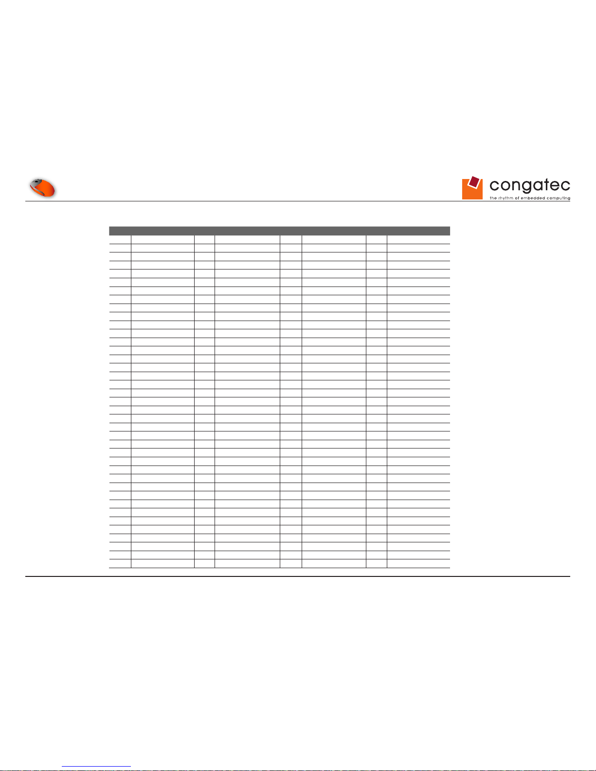
Copyright © 2012 congatec AG CEVA_c_m10 37/47
4.2 Connector Pinout Rows C and D
Pin Row C Pin Row D Pin Row C Pin Row D
C1 GND (FIXED) D1 GND (FIXED) C56 PEG_RX1‑ D56 PEG_TX1‑
C2 IDE_D7 D2 IDE_D5 C57 TYPE1# D57 TYPE2#
C3 IDE_D6 D3 IDE_D10 C58 PEG_RX2+ D58 PEG_TX2+
C4 IDE_D3 D4 IDE_D11 C59
PEG_RX2‑ D59 PEG_TX2‑
C5 IDE_D15 D5 IDE_D12 C60 GND (FIXED) D60 GND (FIXED)
C6 IDE_D8 D6 IDE_D4 C61 PEG_RX3+ D61 PEG_TX3+
C7 IDE_D9 D7 IDE_D0 C62
PEG_RX3‑ D62 PEG_TX3‑
C8 IDE_D2 D8 IDE_REQ C63 RSVD D63 DDPC_CTRLCLK
C9 IDE_D13 D9 IDE_IOW# C64 RSVD D64 DDPC_CTRLDATA
C10 IDE_D1 D10 IDE_ACK# C65 PEG_RX4+ D65 PEG_TX4+
C11 GND (FIXED) D11 GND (FIXED) C66
PEG_RX4‑ D66 PEG_TX4‑
C12 IDE_D14 D12 IDE_IRQ C67 FAN_PWMOUT D67 GND
C13 IDE_IORDY D13 IDE_A0 C68 PEG_RX5+ D68 PEG_TX5+
C14 IDE_IOR# D14 IDE_A1 C69
PEG_RX5‑ D69 PEG_TX5‑
C15 PCI_PME# D15 IDE_A2 C70 GND (FIXED) D70 GND (FIXED)
C16 PCI_GNT2# D16 IDE_CS1# C71 PEG_RX6+ D71 PEG_TX6+
C17 PCI_REQ2# D17 IDE_CS3# C72
PEG_RX6‑ D72 PEG_TX6‑
C18 PCI_GNT1# D18 IDE_RESET# C73 SDVO_DATA D73 SVDO_CLK
C19 PCI_REQ1# D19 PCI_GNT3# C74 PEG_RX7+ D74 PEG_TX7+
C20 PCI_GNT0# D20 PCI_REQ3# C75
PEG_RX7‑ D75 PEG_TX7‑
C21 GND (FIXED) D21 GND (FIXED) C76 GND D76 GND
C22 PCI_REQ0# D22 PCI_AD1 C77 FAN_TACHOIN D77 IDE_CBLID#
C23 PCI_RESET# D23 PCI_AD3 C78 PEG_RX8+ D78 PEG_TX8+
C24 PCI_AD0 D24 PCI_AD5 C79
PEG_RX8‑ D79 PEG_TX8‑
C25 PCI_AD2 D25 PCI_AD7 C80 GND (FIXED) D80 GND (FIXED)
C26 PCI_AD4 D26 PCI_C/BE0# C81 PEG_RX9+ D81 PEG_TX9+
C27 PCI_AD6 D27 PCI_AD9 C82
PEG_RX9‑ D82 PEG_TX9‑
C28 PCI_AD8 D28 PCI_AD11 C83 PP_TPM D83 DDPD_CTRLDATA
C29 PCI_AD10 D29 PCI_AD13 C84 GND D84 GND
C30 PCI_AD12 D30 PCI_AD15 C85 PEG_RX10+ D85 PEG_TX10+
C31 GND (FIXED) D31 GND (FIXED) C86
PEG_RX10‑ D86 PEG_TX10‑
C32 PCI_AD14 D32 PCI_PAR C87 GND D87 GND
C33 PCI_C/BE1# D33 PCI_SERR# C88 PEG_RX11+ D88 PEG_TX11+
C34 PCI_PERR# D34 PCI_STOP# C89
PEG_RX11‑ D89 PEG_TX11‑
C35 PCI_LOCK# D35 PCI_TRDY# C90 GND (FIXED) D90 GND (FIXED)
C36 PCI_DEVSEL# D36 PCI_FRAME# C91 PEG_RX12+ D91 PEG_TX12+
C37 PCI_IRDY# D37 PCI_AD16 C92
PEG_RX12‑ D92 PEG_TX12‑
C38 PCI_C/BE2# D38 PCI_AD18 C93 GND D93 GND
C39 PCI_AD17 D39 PCI_AD20 C94 PEG_RX13+ D94 PEG_TX13+
Page 38
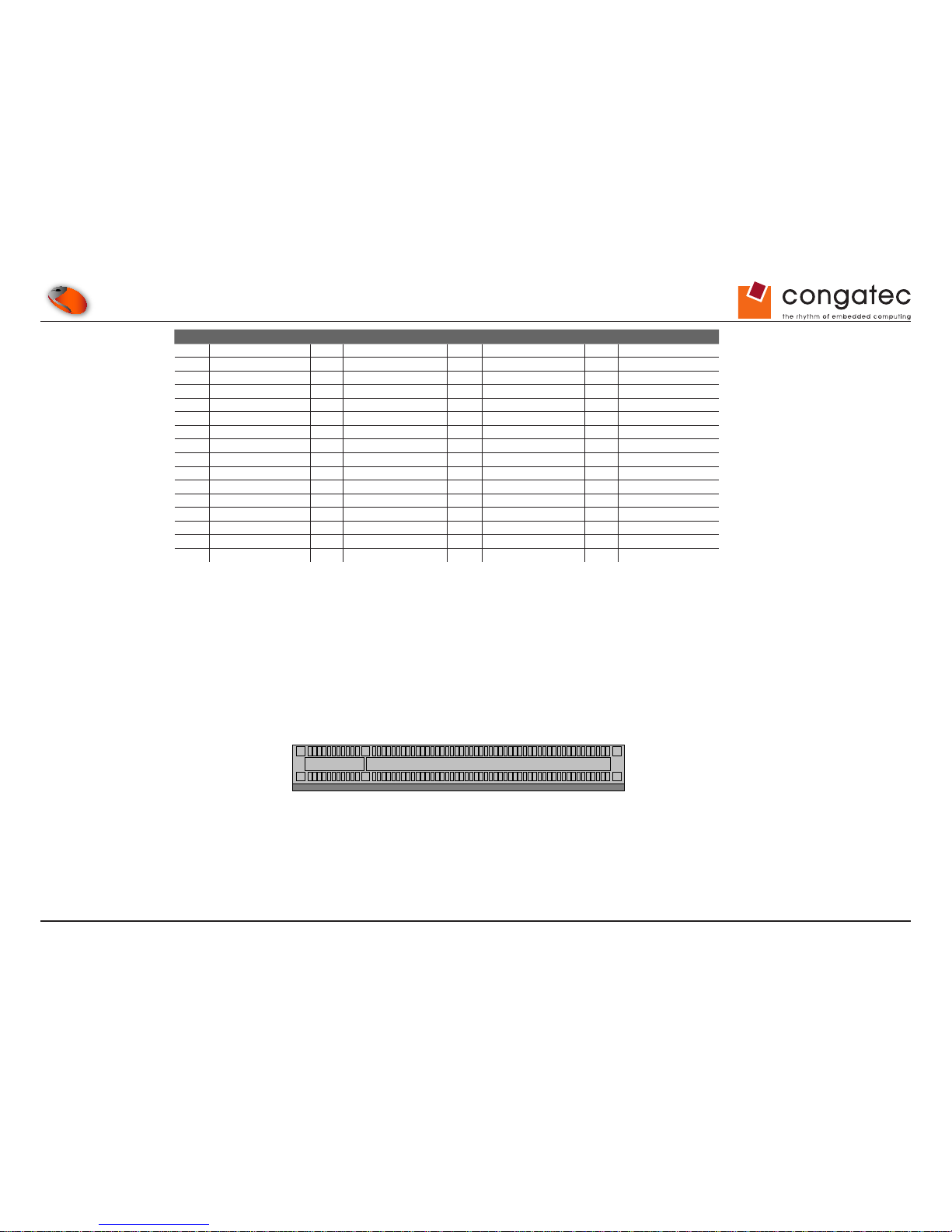
Copyright © 2012 congatec AG CEVA_c_m10 38/47
Pin Row C Pin Row D Pin Row C Pin Row D
C40 PCI_AD19 D40 PCI_AD22 C95 PEG_RX13‑ D95 PEG_TX13‑
C41 GND (FIXED) D41 GND (FIXED) C96 GND D96 GND
C42 PCI_AD21 D42 PCI_AD24 C97 DDPD_CTRLCLK D97 PEG_ENABLE#
C43 PCI_AD23 D43 PCI_AD26 C98 PEG_RX14+ D98 PEG_TX14+
C44 PCI_C/BE3# D44 PCI_AD28 C99
PEG_RX14‑ D99 PEG_TX14‑
C45 PCI_AD25 D45 PCI_AD30 C100 GND (FIXED) D100 GND (FIXED)
C46 PCI_AD27 D46 PCI_IRQC# C101 PEG_RX15+ D101 PEG_TX15+
C47 PCI_AD29 D47 PCI_IRQD# C102
PEG_RX15‑ D102 PEG_TX15‑
C48 PCI_AD31 D48 PCI_CLKRUN# C103 GND D103 GND
C49 PCI_IRQA# D49 PCI_M66EN C104 VCC_12V D104 VCC_12V
C50 PCI_IRQB# D50 PCI_CLK C105 VCC_12V D105 VCC_12V
C51 GND (FIXED) D51 GND (FIXED) C106 VCC_12V D106 VCC_12V
C52 PEG_RX0+ D52 PEG_TX0+ C107 VCC_12V D107 VCC_12V
C53
PEG_RX0‑ D53 PEG_TX0‑ C108 VCC_12V D108 VCC_12V
C54 TYPE0# D54 PEG_LANE_RV# C109 VCC_12V D109 VCC_12V
C55 PEG_RX1+ D55 PEG_TX1+ C110 GND (FIXED) D110 GND (FIXED)
4.2.1 PCI Express Graphics (PEG)
The PEG Port (connector X29) utilizes PCI Express lanes 16‑32 and is suitable to drive a x16 link for an external high‑performance PCI
Express Graphics card. It supports a theoretical bandwidth of up to 4 GB/s. For information about the pinout of the PEG port connector refer to
the 'PCI Express Card Electromechanical Specication, Rev. 1.1'.
(X29)
Page 39
Copyright © 2012 congatec AG CEVA_c_m10 39/47
4.2.2 PATA 100
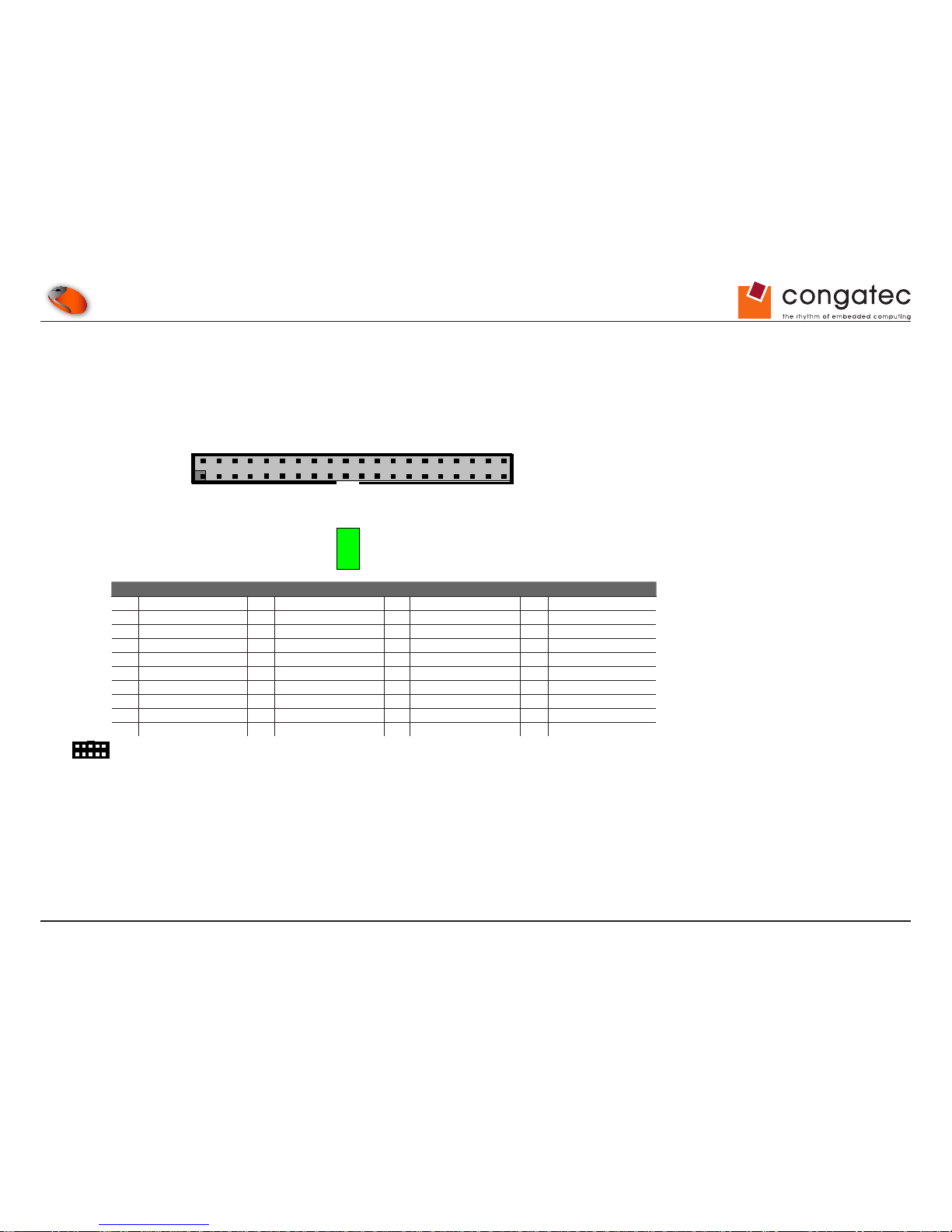
The conga‑CEVAL has one PATA (Parallel ATA) port that is accessible via the X25 connector. The following table lists the pinout for the PATA
port. LED D25 indicates activity on the PATA port.
Pin Signal Pin Signal Pin Signal Pin Signal
1 HDRST# 2 GND 21 IDE_DRQ 22 GND
3 IDE_D7 4 IDE_D8 23 IDE_IOW# 24 GND
5 IDE_D6 6 IDE_D9 25 IDE_IOR# 26 GND
7 IDE_D5 8 IDE_D10 27 IDE_RDY 28 CSEL
9 IDE_D4 10 IDE_D11 29 IDE_ACK 30 GND
11 IDE_D3 12 IDE_D12 31 IDE_INTRQ 32 N.C.
13 IDE_D2 14 IDE_D13 33 IDE_A1 34 CBLID_P#
15 IDE_D1 16 IDE_D14 35 IDE_A0 36 IDE_A2
17 IDE_D0 18 IDE_D15 37 IDE_CS1# 38 IDE_CS3#
19 GND 20 N.C. 39 ACTIVITY 40 GND
Connector Type
X25: 40 pin, 2 row 2.54mm grid box header.
D25
4038
3937363534333231
PATA (X25)
30292827262524232221201918171615141312111098765432
1
4038
3937363534333231302928272625
24232221201918171615141312111098765432
1
Page 40
Copyright © 2012 congatec AG CEVA_c_m10 40/47
4.2.3 CompactFlash Socket
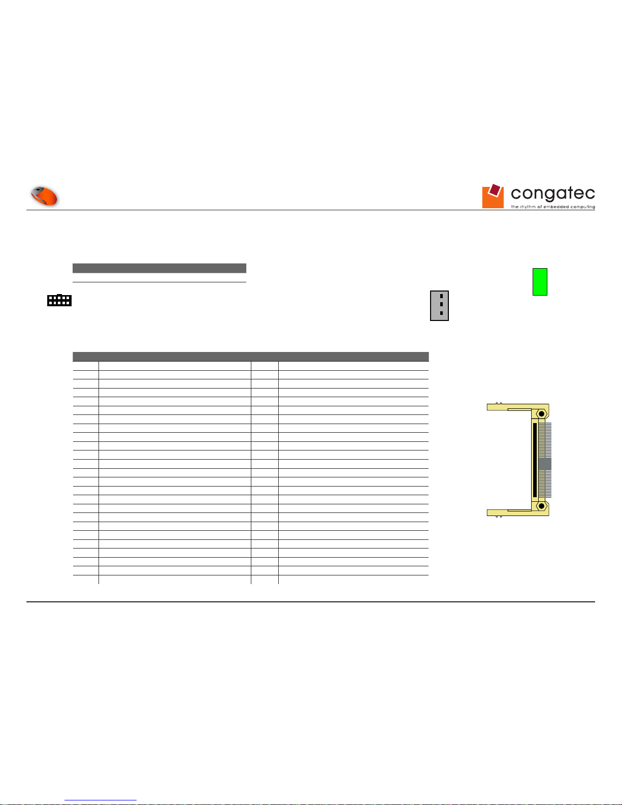
The conga-CEVAL has a CompactFlash socket (X26) that is connected to the PATA port. The CF card can be congured as either a Master or
Slave device through the use of jumper X21. LED D25 indicates activity on the PATA port.
Jumper X21 Conguration
1 ‑ 2 CF Slave (default)
2 ‑ 3 CF Master
Connector Type
X21: 2.54mm grid jumper.
The following table lists the pinout of the CompactFlash socket.
Pin Signal Pin Signal
1 GND 26 CD1
2 IDE_D3 27 IDE_D11
3 IDE_D4 28 IDE_D12
4 IDE_D5 29 IDE_D13
5 IDE_D6 30 IDE_D14
6 IDE_D7 31 IDE_D15
7 IDE_CS1# 32 IDE_CS2#
8 A10 33 VS1
9 OE 34 IDE_IOR#
10 A9 35 IDE_IOW#
11 A8 36 CF_WE#
12 A7 37 IDE_INTRQ
13 +3.3V 38 +3.3V
14 A6 39 CSEL
15 A5 40 N.C.
16 A4 41 HDRST#
17 A3 42 IDE_RDY
18 IDE_A2 43 IDE_DRQ
19 IDE_A1 44 IDE_ACK
20 IDE_A0 45 DASP_CF
21 IDE_D0 46 CBLID_P#
22 IDE_D1 47 IDE_D8
23 IDE_D2 48 IDE_D9
24 N.C. 49 IDE_D10
25 CD2 50 GND
1
2
3
CF Master/Slave
Config
(X21)
D25
Page 41
Copyright © 2012 congatec AG CEVA_c_m10 41/47
4.2.4 PCI BUS
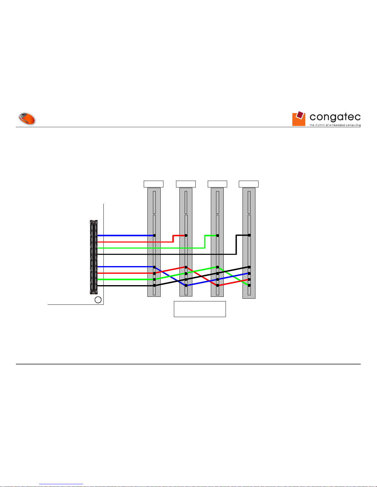
The conga‑CEVAL has four bus master capable PCI bus slots (connectors X30‑X33). The COM Express™
PCI interface is compliant to the
'PCI Local Bus Specication Revision 2.3'. This interface is specied to be +5V tolerant with +3.3V signaling. All necessary PCI bus pull-up
resistors are included on the COM Express™ module. A detailed pin description of the PCI connector can be found in the congatec COM
Express™ Design Guide.
PCI_IRQA#
PCI_IRQB#
PCI_IRQC#
PCI_IRQD#
PCI_AD20
PCI_AD21
PCI_AD22
PCI_AD23
Pin A26
Pin A6
Pin B7
Pin A7
Pin B8
Pin A6
Pin B7
Pin A7
Pin B8
Pin A6
Pin B7
Pin A7
Pin B8
Pin A6
Pin B7
Pin A7
Pin B8
Pin A26
Pin A26
Pin A26
Pin D39
Pin C42
Pin D40
Pin C43
Pin C49
Pin C50
Pin D46
Pin D47
PCI
Slot 1
ID=20
INT A, B, C, D
PCI
Slot 2
ID=21
INT B, C, D, A
PCI
Slot 3
ID=22
INT C, D, A, B
PCI
Slot 4
ID=23
INT D, A, B, C
COM Express™
connector rows C and D
PCI Connector Pin Name
Pin A6: INTA Pin B7: INTB
Pin A7: INTC Pin B8: INTC
Pin A26: IDSEL
COM Express™
Module Type 2
C-D
Page 42
Copyright © 2012 congatec AG CEVA_c_m10 42/47
5 Additional Features
5.1 Reset
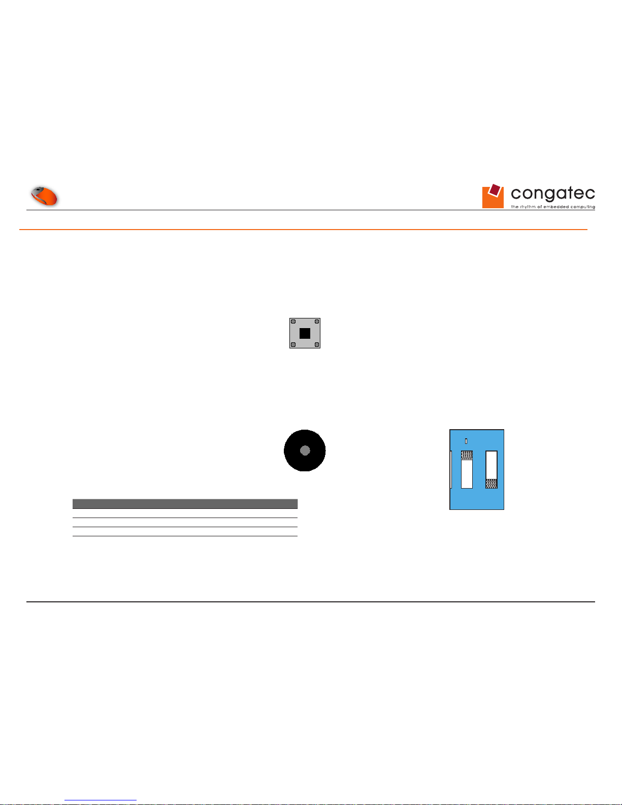
The COM Express™ module and all connected components will perform a hard reset when this button is pressed. The Reset button is
connected to the COM Express™ module's SYS_RESET# signal.
5.2 PC Speaker (Beeper)
The board‑mounted speaker provides audible error code (beep code) information during POST. The speaker M11 is connected to the COM
Express™ module's SPEAKER signal.
The DIP Switch M50 enables or disables the PC beeper as shown below:
DIP Switch M50 Conguration
SW1 On PC beeper enabled (default)
SW1 Off PC beeper disabled
SW2 On Carrier HDA codec disabled
SW2 Off Carrier HDA codec enabled (default)
Reset
(M12)
Speaker
(M11)
21
ON
DIP SWITCH
(M50)
Page 43
Copyright © 2012 congatec AG CEVA_c_m10 43/47
5.3 Debug Display
During the POST (Power On Self Test), the BIOS generates diagnostic progress codes (POST-codes) to different I/O ports (usually port 80h).
If the POST fails, execution stops and the last POST code generated is left at the respective port. This code is useful for determining the point
where an error occurred.
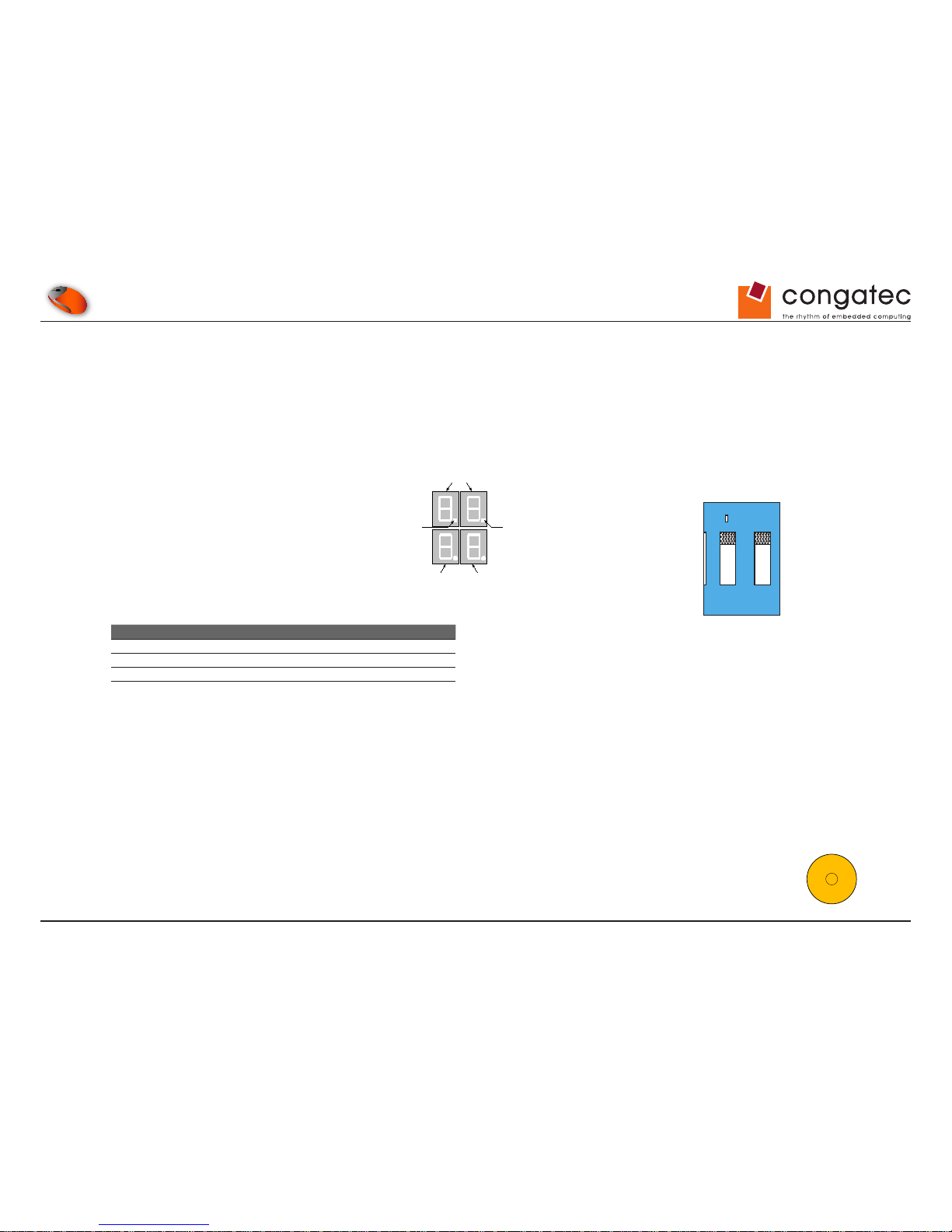
The conga-CEVAL decodes these ports and displays their contents on 4 seven-segment displays (D48 to D51). The dots in the rst two
displays show the state of the Reset and the PCI Frame signals. A list of the POST codes and associated POST test and initialization routines
for the BIOS used on congatec COM Express™ modules is available at www.congatec.com.
The DIP Switch M45 is used for port selection.
DIP Switch M45 Conguration
SW1 On PCI POST (default)
SW1 Off LPC POST
SW2 On POST ADDR 80h/84h (default)
SW2 Off POST ADDR 90h/94h
5.4 TPM Physical Presence Pin
The conga‑CEVAL rev C.X provides an assembly option (R199) to enable the TPM physical presence feature of the COM Express module. The
R199 when populated, pulls the COM Express module pin C83 high, thereby enabling the TPM physical presence feature.
5.5 Ground Test Points
The conga‑CEVAL provides 4 test points that are connected to Ground Potential (M3, M6, M15, and M16). These test
points make it easier to connect oscilloscope probes and/or multimeter lines to Ground when performing measurements
on the COM Express™ module.
Port 80/90
Port 84/90/94
Reset PCI Frame
21
ON
DIP SWITCH
(M45)
Test Points
(TP)
Page 44
Copyright © 2012 congatec AG CEVA_c_m10 44/47
5.6 Fan Connector and Power Conguration
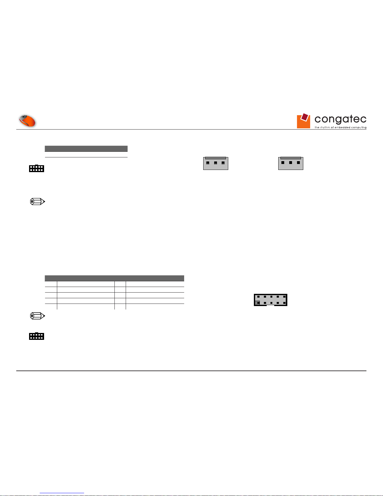
Jumper X63 Conguration
1 ‑ 2 12 Volt fan (default)
2 ‑ 3 5 Volt fan
Connector Type
X14: 3 pin 2.54mm grid fan connector,
X63: 3 pin 2.54mm grid jumper.
Note
congatec COM Express™ modules provide signals for fan control. This has been implemented through the use of some reserved pins.
COM Express™ module pin C77 provides the FAN_T ACHOIN signal that is attached to pin 3 of the fan connector X14 found on the conga-CEV AL.
This signal must receive two pulses per revolution in order to produce an accurate reading and therefore a two pulse per revolution fan is
recommended.
5.7 SMART Battery Management Module
Connector X1 is used to connect the conga-CEVAL to a congatec SMART Battery Management Module evaluation kit. The following table
describes the pinout of the X1 connector.
Pin Signal Pin Signal
1 I2CLK 2 I2DAT
3 PWRBTN#_EXT 4 BATLOW#
5 PS_ON# 6 *SUS_S45#
7 VCC 8 5V_SB
9 SUS_STAT# 10 GND
Note
The asterisk (*) indicates that the signal SUS_S45# is a logical ANDing of SUS_S4# and SUS_S5# signals.
Connector Type
X1: 10 pin, 2 row 2.54 mm grid box header.
1 2 3
Fan
(X14)
1 2 3
Fan Power Config.
(X63)
108
9
7654321
SBM²
(X1)
Page 45
Copyright © 2012 congatec AG CEVA_c_m10 45/47
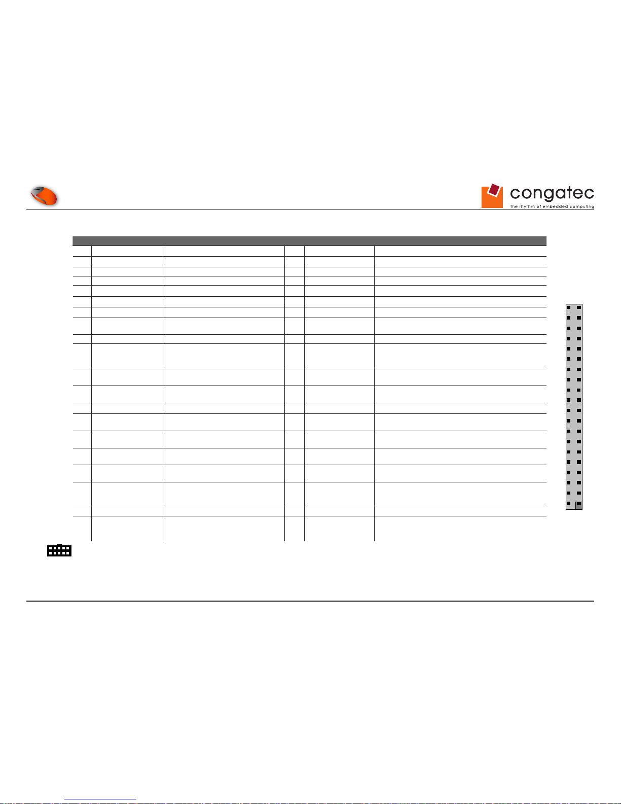
5.8 Feature Connector
Pin Signal Description Pin Signal Description
1 +5V (750 mA fuse) 2 5V_SB (750 mA fuse)
3 +5V (via 330R for LED) 4 Hard Disk Activity Shows activity on hard disk interface IDE1
5 I2DAT General purpose I²C port data I/O line. 6 SMBCLK_SB System Management Bus bidirectional clock line.
7 I2CLK General purpose I²C port clock output. 8 SMBDATA_SB System Management Bus bidirectional data line.
9 TX_CGBC 10 GPO0
11 RX_CGBC 12 GPO1
13 PS_ON# Power Supply On (active low). 14 GPO2
15 SUS_S3# Indicates system is in Suspend to RAM
state. Active low output.
16 GPO3
17 GND Power Ground 18 GND Power Ground
19 THRMTRIP# Active low output indicating that the
CPU has entered thermal shutdown.
20 SMBALRT# System Management Bus Alert – active low input can
be used to generate an SMI# (System Management
Interrupt) or to wake the system.
21 GPI1 22 SUS_S4# Indicates systems is in Suspend to Disk state. Active low
output.
23 SUS_STAT# Indicates imminent suspend operation;
used to notify LPC devices.
24 GPI0
25 GPI2 26 SUS_S5# Indicates systems is in Soft Off state.
27 WDTRIG 28 THRM#
Input from off‑module temp sensor indicating an over‑
temp situation.
29 GPI3 30 PCI_M66EN
Module input signal indicates whether an off‑module PCI
device is capable of 66MHz operation.
31 BATLOW# Indicates that external battery is low. 32 WAKE1# General purpose wake up signal. May be used to
implement wake‑up on PS2 keyboard or mouse activity.
33 PEG_ENABLE# Strap to enable PCI Express x16
external graphics interface.
34 PEG_LANE_RV# PCI Express Graphics lane reversal input strap.
35 KBINH# 36 SYS_RESET# Reset Button Input. Active low input. System is held in
hardware reset while this input is low and comes out of
reset upon release.
37 GND Power Ground 38 GND Power Ground
39 PWBTN# Power Button to bring system out of S5
(soft off), active on rising edge.
40 PWR_OK Power OK from main power supply. A high value
indicates that the power is good. For additional
information refer to PWRGOOD Cong connector X11.
Connector Type
40 pin, 2 row 2.54mm grid header.
4038
3937
36
35
34
33
32
31
30
29
28
27
26
25
24
23
22
21
20
19
18
17
16
15
14
13
12
11
10
9
8
7
6
5
4
3
2
1
4038
3937
36
35
34
33
32
31
30
29
28
27
26
25
24
23
22
21
20
19
18
17
16
15
14
13
12
11
10
9
8
7
6
5
4
3
2
1
4038
3937
36
35
34
33
32
31
Feature
(X27)
30
29
28
27
26
25
24
23
22
21
20
19
18
17
16
15
14
13
12
11
10
9
8
7
6
5
4
3
2
1
4038
3937
36
35
34
33
32
31
30
29
28
27
26
25
24
23
22
21
20
19
18
17
16
15
14
13
12
11
10
9
8
7
6
5
4
3
2
1
Page 46
Copyright © 2012 congatec AG CEVA_c_m10 46/47
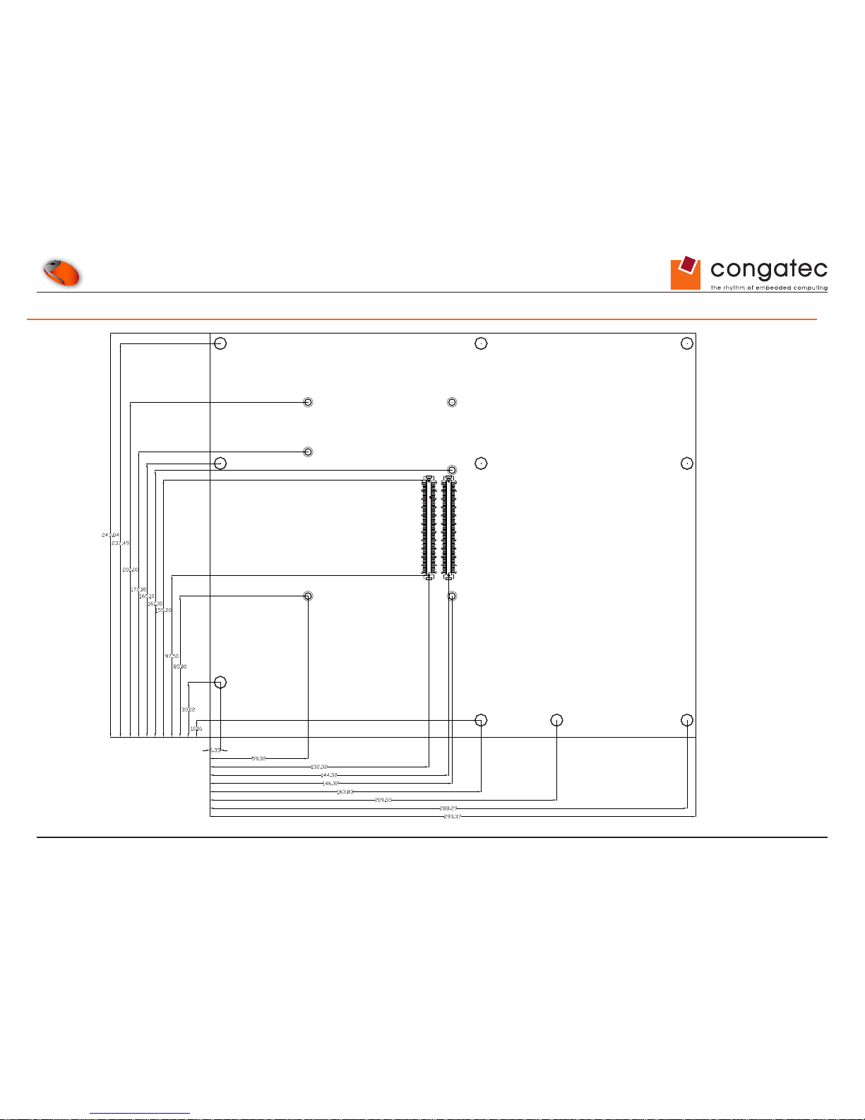
6 Mechanical Drawing conga-CEVAL
Page 47
Copyright © 2012 congatec AG CEVA_c_m10 47/47
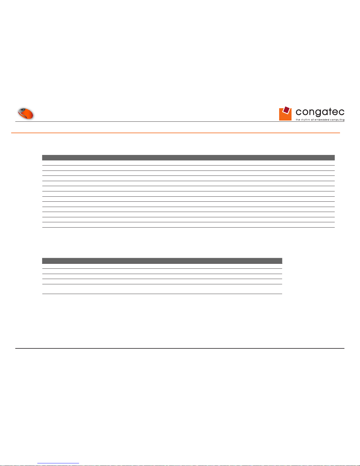
7 Industry Specications
The list below provides links to industry specications that should be used as reference material when designing a COM Express™ carrier
board.
Specication Link
PICMG® COM Express Module™ Base Specication http://www.picmg.org/
PCI Express Base Specication, Revision 2.0 http://www.pcisig.com/specications
PCI Local Bus Specication, Revision 2.3 http://www.pcisig.com/specications
Universal Serial Bus (USB) Specication, Revision 2.0
http://www.usb.org/home
ExpressCard Standard Release 1.0 http://www.expresscard.org/
Serial ATA Specication, Revision 1.0a http://www.serialata.org
Low Pin Count Interface Specication, Revision 1.0 (LPC)
http://developer.intel.com/design/chipsets/industry/lpc.htm
Audio Codec ‘97 Component Specication, Version 2.3
http://www.intel.com/design/chipsets/audio/
High Denition Audio Specication, Rev. 1.0
http://www.intel.com/standards/hdaudio/
LVDS Owner's Manual
http://www.national.com
Extended Display Identication Data Standard Version 1.3 (EDID™) http://www.vesa.org
Enhanced Display Data Channel Specication Version 1.1 (DDC) http://www.vesa.org
IEEE standard 802.3ab 1000BASE T Ethernet http://www.ieee.org/portal/site
Advanced Conguration and Power Interface Specication Rev. 3.0a http://www.acpi.info/
The following reference material from Mindshare Books is recommended by congatec AG. For more information and additional books visit www.mindshare.com.
Title Author
PCI Express System Architecture Ravi Budruk, Don Anderson, Tom Shanley
PCI System Architecture (4th Edition) Tom Shanley, Don Anderson
Universal Serial Bus System Architecture Don Anderson
SATA Storage Technology Don Anderson
Protected Mode Software Architecture
(The PC System Architecture Series)
Tom Shanley
The Unabridged Pentium 4 Tom Shanley
Additional books covering various PC architecture subjects that should be used as reference material can be found at www.intel.com/intelpress.
 Loading...