

CONEX CX28398-24, CX28398-23, CX28398-22, CX28395-19, CX28395-18 Datasheet
...
CX28394/28395/28398
Quad/x16/Octal—T1/E1/J1 Framers
The CX28394/28395/28398 is a family of multiple framers for T1/E1/J1 and Integrated
Service Digital Network (ISDN) primary rate in terfaces operating at 1.5 44 Mbps or 2 .048
Mbps. All framers are totally independent, and each combines a sophisticated framing
synchronizer and transmit/receive slip buffers. Operations are controlled through a
series of memory-mapped registers accessible via a parallel microprocessor port.
Extensive register support is provided for alarm and error monitoring, signaling
supervision (including ISDN D-channel/SS7 process), per-channel trunk conditioning,
and Facility Data Link (FDL) maintenance. A flexible serial Time Division Multiplexed
(TDM) system interface that supports bus rates from 1.536 to 8.192 MHz is featured.
Extensive test and diagnostic functions include a full set of loopbacks, Pseudo Random
Bit Sequence (PRBS) test pattern generation, Bit Error Rate (BER) meter, and forced
error insertion.
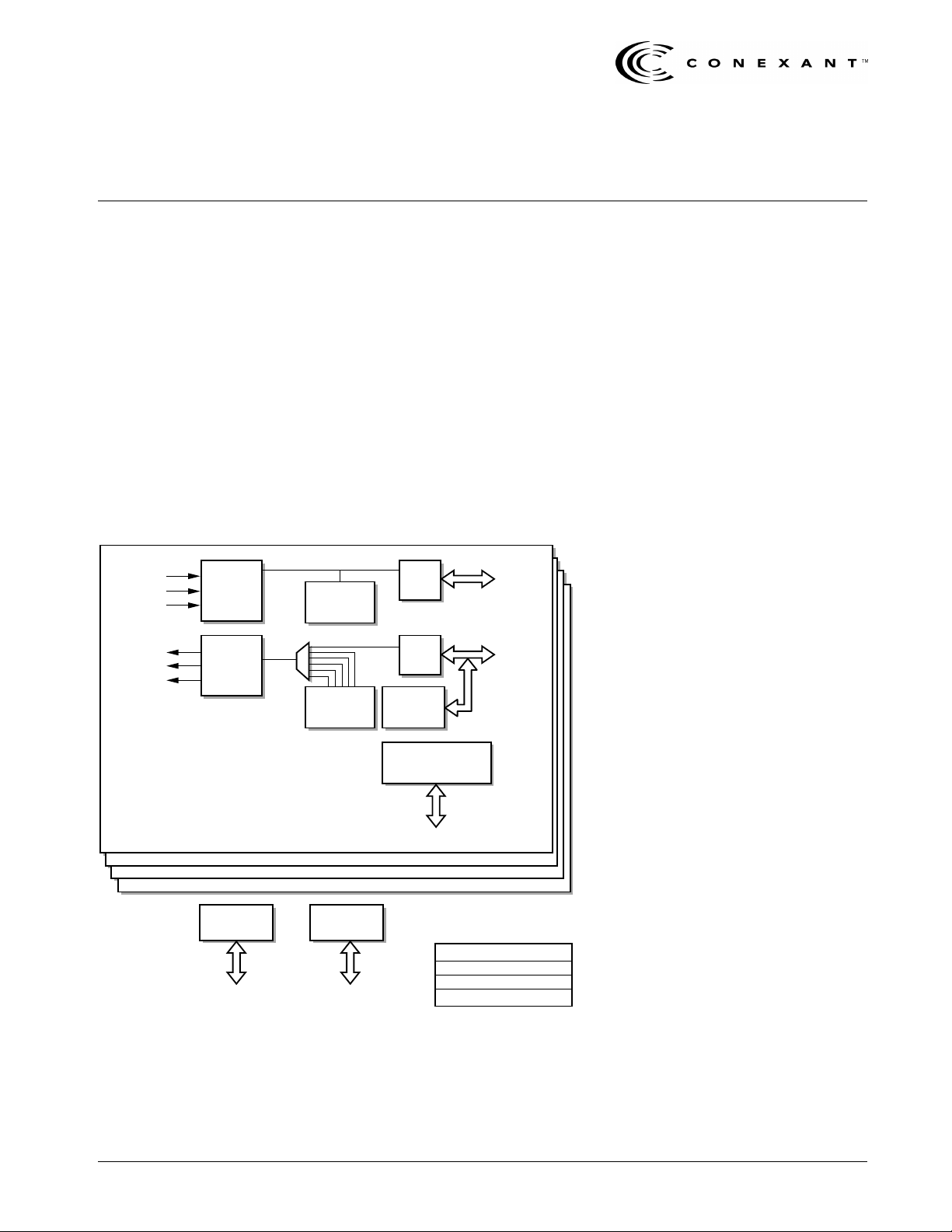
Functional Block Diagram
Receive
Dual Rail or
NRZ
Receive
Dual Rail or
NRZ
Framer #1
.
.
.
Framer #N
* CX28394 and CX28398 only.
Decode
Encode
Test Port
ZCS*
ZCS*
JTAG
T1/E1
Receive
Framer
Overhead
Insertion
Control/Status
Registers
Motorola/Intel
Processor Bus
RX
Slip
Buffer
TX
Slip
Buffer
T1/E1
Transmit
Framer
Data Link Controllers
DL1+DL2
External Data Link
DL3*
CX28394 - 4 Frames
CX28398 - 8 Frames
CX28395 - 16 Frames
Receive
System
Bus
Transmit
System
Bus
Framer #N
8394-8-5_019
Distinguishing Features
• Up to 16 T1/E1/J1 Framers i n one
package
• Extensive support of variou s
protocols
• T1: SF, ESF, SLC
TTC JT(J1)
• E1: PCM-30, G.704, G.706, G.732,
ISDN primary rate (ETS300 011,
INS 500)
• Extracts and inserts signaling bits
• Dual HDLC controllers per framer for
data link and LAPD/SS7 signaling
• Two-fr ame tran smit an d recei ve PCM
slip buffers
• Separate or multiplexed system bus
interfaces
• Parallel 8-bit microprocessor port
supports Intel or Motorola buses
• BERT generation and counting
• B8ZS/HDB3/Bit 7 zero suppression
(CX28394 and CX28398 only)
• Operates from a single +3.3 V dc
± 5% power supply
• Low-power CM OS tec h no lo gy
Applications
• Multiline T1/E1 Channel Service
Unit/Data Service Unit (CSU/DSU)
• Digital Access Cross-Connect
System (DACS)
• T1/E1 Multiple xe r (MUX )
• PBXs and PCM channel bank
• ISDN Primary Rate Access (PRA)
• Frame Relay Switches and Access
Devices (FRADS)
• SONET/SDH add/drop multiplexers
• T3/E3 channelized access
concentrators
®
96, T1DM,
Data Sheet 100054E
June 2000
CX28398EVM—Evaluation Module, Octal T1/E1 ISDN PRI Board
T1 or E1 Connection at DSX Levels
Quad T1/E1 LIU (CX28380) Quad T1/E1 LIU (CX28380)
Address
Bus
Microprocessor
Data
Bus
12
8
CX28398 (Octal T1/E1 Framer)
Local PCM Highway (i.e., 2 @ 8192 kbps)
8394-8-5_012
© 1999, 2000, Conexant Systems, Inc.
All Rights Reserved.
Information in this document is provided in connection with Conexant Systems, Inc. (“Conexant”) products. These materials are
provided by Conexant as a service to its customers and may be used for informational purposes only. Conexant assumes no
responsibility for errors or omissions in these materials. Conexant may make changes to specifications and product descript ion s at
any time, without notice. Conexant makes no commitment to update the information and shall have no responsibility whatsoever for
conflicts or incompatibilities arising from future changes to its specifications and product descriptions.
No license, express or implied, by estoppel or otherwise, to any intellectual property rights is granted by this document. Except as
provided in Conexant’s Terms and Conditions of Sale for such products, Conexant assumes no liability whatsoever.
THESE MATERIALS ARE PROVIDED “AS IS” WITHOUT WARRANTYOF ANY KIND, EITHER EXPRESS OR IMPLIED, RELATING
TO SALE AND/OR USE OF CONEXANT PRODUCTS INCLUDING LIABILITY OR WARRANTIES RELATING TO FITNESS FOR A
PARTICULARPURPOSE, CONSEQUENTIAL OR INCIDENTAL DAMAGES,MERCHANTABILITY, OR INFRINGEMENT OF ANY
PATENT, COPYRIGHT OR OTHER INTELLECTUAL PROPERTYRIGHT. CONEXANT FURTHER DOES NOT WARRANT THE
ACCURACY OR COMPLETENESS OF THE INFORMATION, TEXT, GRAPHICS OR OTHER ITEMS CONTAINED WITHIN THESE
MATERIALS. CONEXANT SHALL NOT BE LIABLE FOR ANY SPECIAL, INDIRECT, INCIDENTAL, OR CONSEQUENTIAL
DAMAGES,INCLUDING WITHOUT LIMITATION, LOST REVENUES OR LOST PROFITS, WHICH MAYRESULT FROM THE USE
OF THESE MATERIALS.
Conexant products ar e not intended for use in medical, lifesaving or life sustaining applications. Conexant customers using or selling
Conexant products for use in such applications do so at their own risk and agree to fully indemnify Conexant for any damages
resulting from such improper use o r sale.
The following are trademarks of Conexant Systems, Inc.: Conexant™, the Conexant C symbol, and “What’s Next in Communications
Te chnologies”™. Product names or services listed in this publication are for identification purposes only, and may be trademark s of
third parties. Third-par ty brands and names are the property of their respective owners.
For additional disclaimer information, please consult Conexant’s Legal Information posted at www.conexant.com,whichis
incorporated by reference.
Reader Response: Conexant strives to produce quality documentation and welcomes your feedback. Please send comments and
suggestions to tech.pubs@conexant.com. For tec hnical questions, contact your local Conexant sales office or field applicat ions
engineer.
100054E Conexant
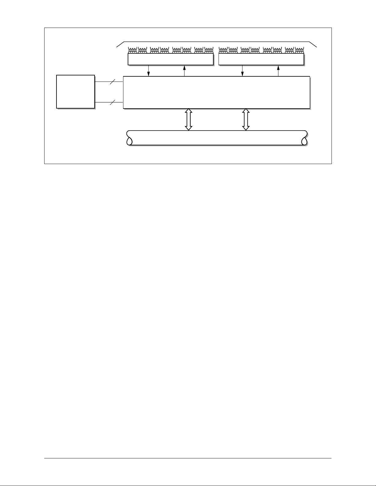
Typical Quad T1/E1 Application
Address
Bus
Microprocessor
Data
Bus
Typical x16 T1/E1 Application
12
T1 or E1 Connection at DSX Levels
CX28380 (Quad LIU)
CX28394 (Octal T1/E1 Framer)
8
Local PCM Highway (8192 kbps)
8394-8-5_015
T1 or E1 Line Interfaces, SONET/SDH Mapper or M13/E13 Mux
Address
Bus
Microprocessor
Data
Bus
Selects
12
8
2
Chip
CX28395 ( x16 T1/E1 Framer)
Local PCM Highways 32 at 1536 kbps to 8 at 8192 kbps)
CX28395 ( x16 T1/E1 Framer)
2
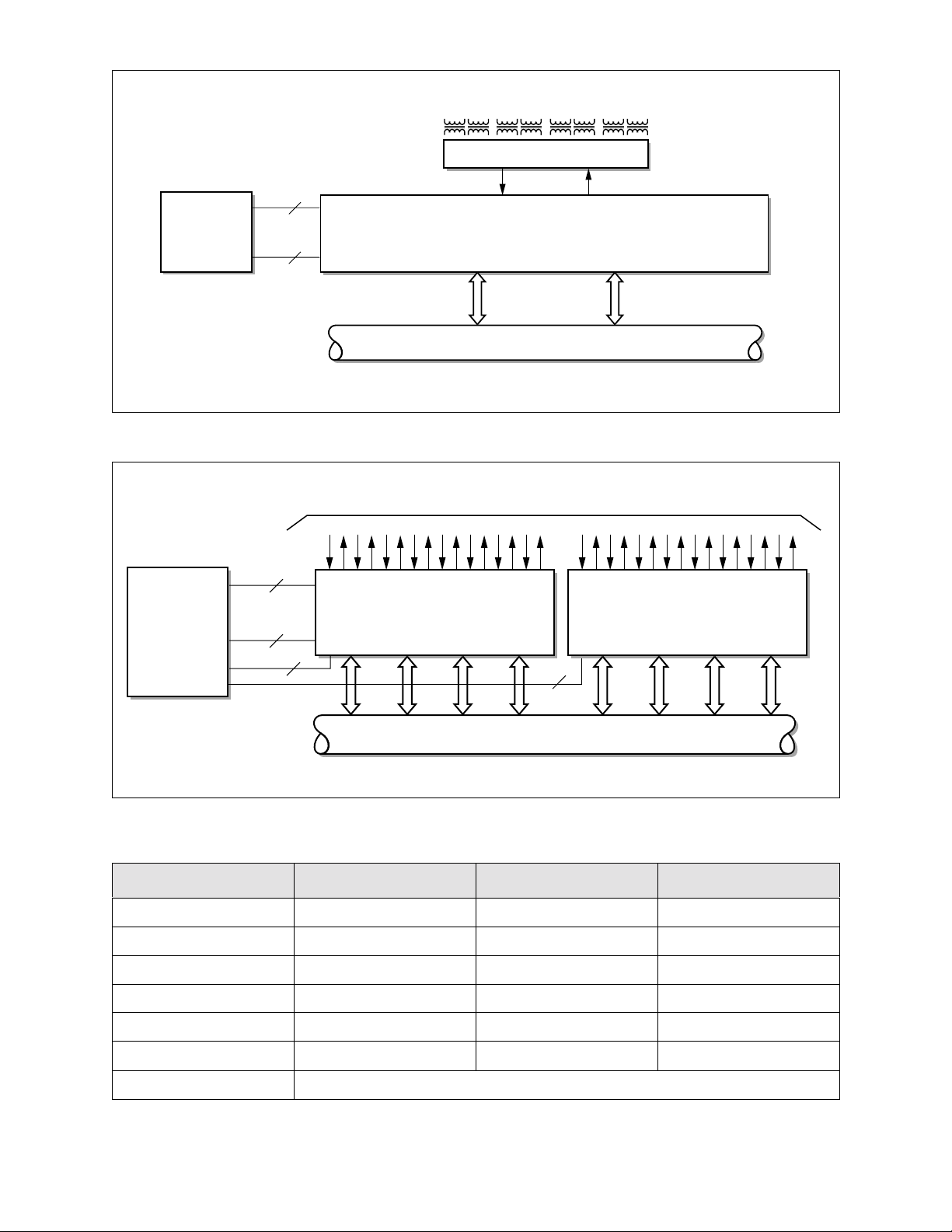
Ordering Information
Model Number Number of Framers Package Operating Temperature
CX28394-22 4 128-pin TQFP –40 to 85 °C
CX28398-22 8 208-pin PQFP –40 to 85 °C
CX28398-23 8 272-pin B G A –40 to 85 °C
CX28395-19 16 318-pin BGA –40 to 85 °C
8394-8-5_014
CX28395-18 16 318-pin BGA 0 to 70 °C
CX28398-24 8 208-pin CABGA –40 to 85 °C
BT00-D660-00 1 CX28398/CX283 80 Ev a lu a t io n Mod ule
100054E Conexant

Detailed Feature Summary
Frame Alignm ent
• Framed formats:
– Independent transm it and receive
framing modes
– T1: FT/SF/ESF/SLC/T1DM/TTC-JT(J1)
– E1: FAS/MFAS/FAS+CAS/MFAS+CAS
• Maximum Average Reframe Time
(MART) less than 50 ms
• Transmitter alignment modes:
– Align to system bus data
– Align to system bus sync
– Align to buffer data (embedded
framing)
• Unframed mode
Signaling
• T1: 2-, 4-, or 16-state robbed bit
ABCD signaling
• E1: Channel Associated Signaling
(CAS)
• Common Chann el Si gn a lin g (CCS) in
any time slot
• Per-channel receive signaling stack
• Signaling state change interrupt
• Automatic and manual signaling
freeze
• Debounce signaling (2-bit
integration)
• UNICODE detection
• Signaling reinsertion on PCM system
bus
• Separat e I /O fo r sys te m bu s s ign al in g
• Per-channel tr ansparent
Loopbacks
• Remote loop ba c k toward line
– Retains BPV transparency
(CX28394 and CX28398 only)
• Payload loopback
• Per-channel D S0 remote loopback
• Local loopback towards system
– Framer digital loopback
– Per-channel DS0 local loopback
• Inband loop ba c k co d e dete c t io n/
generation
• Simultaneous local and remote line
loopbacks
Processor Interface
• Parallel 8-bit bu s
• Data strobes (Motorola) or address
latch enable (Intel)
• Multiplexed or non-multiplexed
address/data bus
• Synchronous or asynchronous
data transfers
• Open drain interru pt ou tput with
maskable sources
Out-of-Service Testing
and Maintenance
• Pseudo-Random Bit Sequence
(PRBS):
– Independent transmit and receive
11
–2
; 215; 220; 223 patterns
– Framed or unframe d mode
– Optional 7/14 zero limit
– Bit Error Counter (BERR)
• Single error insertion:
– PRBS error
– Framing error
– CRC error
– BPV/LCV error (C X28394 and
CX28398 only)
– COFA error
System Bus Interface (SBI)
• System bus data rates :
– 1536 kbps (T1 without F-bits)
– 1544 kbps (T1)
– 2048 kbps (E1)
– 4096 kbps (2E1)
– 8192 kbps (4E1)
• Clock operation at 1x or 2x data rate
• Selectable I/O clock edges
• Master, slave, or mixed bus timi ng
• Bit and time slot frame sync offsets
• DS0 drop/insert indicators for
external mux
• Embedded T1 framing transport
per G.802
• Receive and transmit slip buffers
– Bypass, 2-frame, or 64-bit depth
– Slip detection with directi onal
status
– Slip buffer phase status
– Per-channel idle code insertion
– Processor accessible data buffers
• Direct connection to upper layer
devices:
– Link layer: Bt8474
– ATM layer: CN8228
• Direct connection to physical line
interface
– CX28380
• Supported system bus formats:
– ATT Concentration Highway
Interface (CHI)
– Multi-Vendor Integration Protocol
(MVIP)
–Mitel ST-bus
• Separate or internally multiplexed
bus modes
In-Service
Performance Monitoring
• One-second timer I/O to synchronize
reporting
• Receive error detectors with
accumulators:
– Bipolar/Line Code Violations
(LCV) (CX28394 and CX28398
only)
– Excessive Zeros (EXZ)
– Loss of Frame (RLOF)
– Framing Errors (FERR)
– CRC Errors (CERR)
– Far End Block Errors (FEBE)
– Severely Errored Frames (SEF)
– Change of Frame Alignment
(COFA)
• Transmit error detectors:
– Loss of Frame (TLOF)
– Framing Errors (TFERR)
– Multiframe Errors (TMERR)
– CRC Errors (TCERR)
– Loss of Transmit Clock (TL OC )
• Receive alarm detectors:
– Alarm Indication Signal (AIS)
– Loss of Signal (RLOS)
– RAI/Yellow Alarm (YEL)
– Multiframe Yellow (MYEL)
– Lost Frame Alignment (FRED )
– Lost Multiframe Alignment
(MRED)
– Carrier Failure Alarm (CFA) with
8:1 dual slope integrat ion
• Controlled Frame Slip (RFS LIP)
Uncontrolled Frame Slip (RUSLI P)
• Automatic and on-de m and transmit
alarms:
– AIS following RLOS and/or TLOC
– Automatic AIS clock switching
– YEL following FRED
– YEL following 100ms reframe
timeout
– MYEL followin g MRE D
– FEBE followin g C ER R
100054E Conexant

Data Links
• Two full-featured data link controllers
(DL1 and DL2):
– 64-octet transmit and receive
FIFOs
– HDLC Message Oriented Protoc ol
(MOP)
– Unformatted data transfer
– Unformatted circular buffer
– End of message/buffer interrupt
– Near full/empty interrupts at
selected depth
• Access any bit combination in any
time slot:
– ISDN D-channels at 16, 32, or 64
kbps
– National/spare bits (SA- bits) in 4
kbps increments
– CCS/SS7
– T1DM R-bits
• Access T1 F-bits in even, odd , or all
frames:
– Automatic Performance Report
Message (PRM) generator
– ESF Facility Data Link (FDL)
– Unformatted SLC-96 overhead
– Bit-Oriented Protocol (BOP)
priority codeword generation and
detection
• Separate I/O for external data link
(DL3) on CX2839 4 and CX28398
devices
100054E Conexant

100054E Conexant

Table of Contents
List of Figures . . . . . . . . . . . . . . . . . . . . . . . . . . . . . . . . . . . . . . . . . . . . . . . . . . . . . . . . . . . . . . . . . . . . . . . . xv
List of Tables . . . . . . . . . . . . . . . . . . . . . . . . . . . . . . . . . . . . . . . . . . . . . . . . . . . . . . . . . . . . . . . . . . . . . . . . . xvii
1.0 Product Description. . . . . . . . . . . . . . . . . . . . . . . . . . . . . . . . . . . . . . . . . . . . . . . . . . . . . . . . . . . . . 1-1
1.1 Overview. . . . . . . . . . . . . . . . . . . . . . . . . . . . . . . . . . . . . . . . . . . . . . . . . . . . . . . . . . . . . . . . . . 1-1
1.1.1 External Datalink . . . . . . . . . . . . . . . . . . . . . . . . . . . . . . . . . . . . . . . . . . . . . . . . . . . . . . 1-1
1.1.2 RINDO/TINDO . . . . . . . . . . . . . . . . . . . . . . . . . . . . . . . . . . . . . . . . . . . . . . . . . . . . . . . . 1-1
1.1.3 LIU Serial Port . . . . . . . . . . . . . . . . . . . . . . . . . . . . . . . . . . . . . . . . . . . . . . . . . . . . . . . . 1-2
1.1.4 Transmit/Receive Line Interface . . . . . . . . . . . . . . . . . . . . . . . . . . . . . . . . . . . . . . . . . . . 1-2
1.2 Pin Assignments. . . . . . . . . . . . . . . . . . . . . . . . . . . . . . . . . . . . . . . . . . . . . . . . . . . . . . . . . . . . 1-3
2.0 Circuit Description. . . . . . . . . . . . . . . . . . . . . . . . . . . . . . . . . . . . . . . . . . . . . . . . . . . . . . . . . . . . . . 2-1
2.1 Functional Block Diagram. . . . . . . . . . . . . . . . . . . . . . . . . . . . . . . . . . . . . . . . . . . . . . . . . . . . . 2-1
2.2 Receiver . . . . . . . . . . . . . . . . . . . . . . . . . . . . . . . . . . . . . . . . . . . . . . . . . . . . . . . . . . . . . . . . . . 2-4
2.2.1 ZCS Decoder . . . . . . . . . . . . . . . . . . . . . . . . . . . . . . . . . . . . . . . . . . . . . . . . . . . . . . . . . 2-4
2.2.2 In-Band Loopback Code Detection . . . . . . . . . . . . . . . . . . . . . . . . . . . . . . . . . . . . . . . . . 2-5
2.2.3 Error Count ers . . . . . . . . . . . . . . . . . . . . . . . . . . . . . . . . . . . . . . . . . . . . . . . . . . . . . . . . 2-5
2.2.3.1 Frame Bit Err or Counter. . . . . . . . . . . . . . . . . . . . . . . . . . . . . . . . . . . . . . . . . 2-6
2.2.3.2 CRC Error Counter . . . . . . . . . . . . . . . . . . . . . . . . . . . . . . . . . . . . . . . . . . . . 2-6
2.2.3.3 LCV Error Counter. . . . . . . . . . . . . . . . . . . . . . . . . . . . . . . . . . . . . . . . . . . . . 2-6
2.2.3.4 FEBE Counter . . . . . . . . . . . . . . . . . . . . . . . . . . . . . . . . . . . . . . . . . . . . . . . . 2-6
2.2.4 Error Monito r. . . . . . . . . . . . . . . . . . . . . . . . . . . . . . . . . . . . . . . . . . . . . . . . . . . . . . . . . 2-6
2.2.4.1 Frame Bit Error . . . . . . . . . . . . . . . . . . . . . . . . . . . . . . . . . . . . . . . . . . . . . . . 2-6
2.2.4.2 MFAS Error. . . . . . . . . . . . . . . . . . . . . . . . . . . . . . . . . . . . . . . . . . . . . . . . . . 2-7
2.2.4.3 CAS Error . . . . . . . . . . . . . . . . . . . . . . . . . . . . . . . . . . . . . . . . . . . . . . . . . . . 2-7
2.2.4.4 CRC Error . . . . . . . . . . . . . . . . . . . . . . . . . . . . . . . . . . . . . . . . . . . . . . . . . . . 2-7
2.2.4.5 Pulse Density Violation . . . . . . . . . . . . . . . . . . . . . . . . . . . . . . . . . . . . . . . . . 2-7
100054E Conexant vii

Table of Contents CX28394/28395/28398
Quad/x16/Octal—T1/E1/J1 Framers
2.2.5 Alarm Monitor . . . . . . . . . . . . . . . . . . . . . . . . . . . . . . . . . . . . . . . . . . . . . . . . . . . . . . . . 2-7
2.2.5.1 Loss of Frame. . . . . . . . . . . . . . . . . . . . . . . . . . . . . . . . . . . . . . . . . . . . . . . . 2-8
2.2.5.2 Loss of Signal. . . . . . . . . . . . . . . . . . . . . . . . . . . . . . . . . . . . . . . . . . . . . . . . 2-8
2.2.5.3 Receive Analog Loss of Signal. . . . . . . . . . . . . . . . . . . . . . . . . . . . . . . . . . . . 2-8
2.2.5.4 Alarm Indication Signa l . . . . . . . . . . . . . . . . . . . . . . . . . . . . . . . . . . . . . . . . . 2-8
2.2.5.5 Yellow Alarm. . . . . . . . . . . . . . . . . . . . . . . . . . . . . . . . . . . . . . . . . . . . . . . . . 2-8
2.2.5.6 Multiframe YEL. . . . . . . . . . . . . . . . . . . . . . . . . . . . . . . . . . . . . . . . . . . . . . . 2 -9
2.2.5.7 Severely Errored Frame. . . . . . . . . . . . . . . . . . . . . . . . . . . . . . . . . . . . . . . . . 2-9
2.2.5.8 Change of Frame Alignment. . . . . . . . . . . . . . . . . . . . . . . . . . . . . . . . . . . . . . 2-9
2.2.5.9 Receive Multiframe AIS. . . . . . . . . . . . . . . . . . . . . . . . . . . . . . . . . . . . . . . . . 2-9
2.2.6 Test Pattern Receiver . . . . . . . . . . . . . . . . . . . . . . . . . . . . . . . . . . . . . . . . . . . . . . . . . . . 2-9
2.2.7 Receive Framing. . . . . . . . . . . . . . . . . . . . . . . . . . . . . . . . . . . . . . . . . . . . . . . . . . . . . . 2-10
2.2.8 External Receive Data Link (CX28394 and CX28398 Only) . . . . . . . . . . . . . . . . . . . . . . . 2-15
2.2.9 Sa-Byte Receive Buffers . . . . . . . . . . . . . . . . . . . . . . . . . . . . . . . . . . . . . . . . . . . . . . . . 2-15
2.2.10 Receive Data Link. . . . . . . . . . . . . . . . . . . . . . . . . . . . . . . . . . . . . . . . . . . . . . . . . . . . . 2-16
2.2.10.1 Data Link C ontrollers. . . . . . . . . . . . . . . . . . . . . . . . . . . . . . . . . . . . . . . . . . 2-16
2.2.10.2 RBOP Receiver . . . . . . . . . . . . . . . . . . . . . . . . . . . . . . . . . . . . . . . . . . . . . . 2-20
2.3 System Bus. . . . . . . . . . . . . . . . . . . . . . . . . . . . . . . . . . . . . . . . . . . . . . . . . . . . . . . . . . . . . . . 2-21
2.3.1 Non-Multiplexed Mode. . . . . . . . . . . . . . . . . . . . . . . . . . . . . . . . . . . . . . . . . . . . . . . . . 2-21
2.3.2 Externally Multiplexed Mode. . . . . . . . . . . . . . . . . . . . . . . . . . . . . . . . . . . . . . . . . . . . . 2-22
2.3.3 Internally Multiplexed Mode . . . . . . . . . . . . . . . . . . . . . . . . . . . . . . . . . . . . . . . . . . . . . 2-23
2.3.4 Receive System Bus. . . . . . . . . . . . . . . . . . . . . . . . . . . . . . . . . . . . . . . . . . . . . . . . . . . 2-24
2.3.4.1 Timebase . . . . . . . . . . . . . . . . . . . . . . . . . . . . . . . . . . . . . . . . . . . . . . . . . . 2-28
2.3.4.2 Slip Buffer . . . . . . . . . . . . . . . . . . . . . . . . . . . . . . . . . . . . . . . . . . . . . . . . . 2-28
2.3.4.3 Signaling Buffer . . . . . . . . . . . . . . . . . . . . . . . . . . . . . . . . . . . . . . . . . . . . . 2-30
2.3.4.4 Signaling Stack . . . . . . . . . . . . . . . . . . . . . . . . . . . . . . . . . . . . . . . . . . . . . . 2-31
2.3.4.5 Embedded Framing. . . . . . . . . . . . . . . . . . . . . . . . . . . . . . . . . . . . . . . . . . . 2-31
2.3.5 Transmit System Bus . . . . . . . . . . . . . . . . . . . . . . . . . . . . . . . . . . . . . . . . . . . . . . . . . . 2-32
2.3.5.1 Timebase . . . . . . . . . . . . . . . . . . . . . . . . . . . . . . . . . . . . . . . . . . . . . . . . . . 2-35
2.3.5.2 Slip Buffer . . . . . . . . . . . . . . . . . . . . . . . . . . . . . . . . . . . . . . . . . . . . . . . . . 2-35
2.3.5.3 Signaling Buffer . . . . . . . . . . . . . . . . . . . . . . . . . . . . . . . . . . . . . . . . . . . . . 2-36
2.3.5.4 Transmit Framing . . . . . . . . . . . . . . . . . . . . . . . . . . . . . . . . . . . . . . . . . . . . 2-36
2.3.5.5 Embedded Framing. . . . . . . . . . . . . . . . . . . . . . . . . . . . . . . . . . . . . . . . . . . 2-39
2.4 T ransmitter . . . . . . . . . . . . . . . . . . . . . . . . . . . . . . . . . . . . . . . . . . . . . . . . . . . . . . . . . . . . . . . 2-40
2.4.1 External Transmit Data Link (CX28394 and CX28398 Only) . . . . . . . . . . . . . . . . . . . . . . 2-41
2.4.2 Transmit Data Links . . . . . . . . . . . . . . . . . . . . . . . . . . . . . . . . . . . . . . . . . . . . . . . . . . . 2-41
2.4.2.1 Data Link C ontrollers. . . . . . . . . . . . . . . . . . . . . . . . . . . . . . . . . . . . . . . . . . 2-41
2.4.2.2 Circular Buffer. . . . . . . . . . . . . . . . . . . . . . . . . . . . . . . . . . . . . . . . . . . . . . . 2-42
2.4.2.3 Time Slot and Bit Selection . . . . . . . . . . . . . . . . . . . . . . . . . . . . . . . . . . . . . 2-43
2.4.2.4 Transmit Data Link FIFO Buffer . . . . . . . . . . . . . . . . . . . . . . . . . . . . . . . . . . 2-43
2.4.2.5 End of Message . . . . . . . . . . . . . . . . . . . . . . . . . . . . . . . . . . . . . . . . . . . . . 2-43
2.4.2.6 Programmi ng the Data Li nk Controller . . . . . . . . . . . . . . . . . . . . . . . . . . . . . 2-44
2.4.2.7 PRM Genera tor. . . . . . . . . . . . . . . . . . . . . . . . . . . . . . . . . . . . . . . . . . . . . . 2-46
2.4.2.8 TBOP Transceiver . . . . . . . . . . . . . . . . . . . . . . . . . . . . . . . . . . . . . . . . . . . . 2-46
viii Conexant 100054E

CX28394/28395/28398 Table of Contents
Quad/x16/Octal—T1/E1/J1 Framers
2.4.3 Sa-Byte Overwrite Buffer . . . . . . . . . . . . . . . . . . . . . . . . . . . . . . . . . . . . . . . . . . . . . . . 2-46
2.4.4 Overhead Pattern Generation . . . . . . . . . . . . . . . . . . . . . . . . . . . . . . . . . . . . . . . . . . . . 2-47
2.4.4.1 Framing Pattern Generation. . . . . . . . . . . . . . . . . . . . . . . . . . . . . . . . . . . . . 2-47
2.4.4.2 Alarm Generation . . . . . . . . . . . . . . . . . . . . . . . . . . . . . . . . . . . . . . . . . . . . 2-47
2.4.4.3 CRC Generation . . . . . . . . . . . . . . . . . . . . . . . . . . . . . . . . . . . . . . . . . . . . . 2-49
2.4.4.4 Far-End Block Erro r Generation . . . . . . . . . . . . . . . . . . . . . . . . . . . . . . . . . . 2-49
2.4.5 Test Pattern Generation . . . . . . . . . . . . . . . . . . . . . . . . . . . . . . . . . . . . . . . . . . . . . . . . 2-50
2.4.6 Transmit Error Insertion . . . . . . . . . . . . . . . . . . . . . . . . . . . . . . . . . . . . . . . . . . . . . . . . 2-50
2.4.7 In-Band Loopback Code Generation . . . . . . . . . . . . . . . . . . . . . . . . . . . . . . . . . . . . . . . 2-51
2.4.8 ZCS Encoder . . . . . . . . . . . . . . . . . . . . . . . . . . . . . . . . . . . . . . . . . . . . . . . . . . . . . . . . 2-51
2.5 Microp rocessor Interface . . . . . . . . . . . . . . . . . . . . . . . . . . . . . . . . . . . . . . . . . . . . . . . . . . . . 2-55
2.5.1 Address/Data Bus. . . . . . . . . . . . . . . . . . . . . . . . . . . . . . . . . . . . . . . . . . . . . . . . . . . . . 2-56
2.5.2 Bus Control Signals . . . . . . . . . . . . . . . . . . . . . . . . . . . . . . . . . . . . . . . . . . . . . . . . . . . 2-56
2.5.3 Interrupt Requests. . . . . . . . . . . . . . . . . . . . . . . . . . . . . . . . . . . . . . . . . . . . . . . . . . . . 2-56
2.5.4 Device Reset . . . . . . . . . . . . . . . . . . . . . . . . . . . . . . . . . . . . . . . . . . . . . . . . . . . . . . . . 2-58
2.6 Loopbacks. . . . . . . . . . . . . . . . . . . . . . . . . . . . . . . . . . . . . . . . . . . . . . . . . . . . . . . . . . . . . . . . 2-59
2.6.1 Remote Line Loopback. . . . . . . . . . . . . . . . . . . . . . . . . . . . . . . . . . . . . . . . . . . . . . . . . 2-59
2.6.2 Remote Payload Loopback. . . . . . . . . . . . . . . . . . . . . . . . . . . . . . . . . . . . . . . . . . . . . . 2-59
2.6.3 Remote Per-Channel Loopback. . . . . . . . . . . . . . . . . . . . . . . . . . . . . . . . . . . . . . . . . . . 2-59
2.6.4 Local Framer Loopback . . . . . . . . . . . . . . . . . . . . . . . . . . . . . . . . . . . . . . . . . . . . . . . . 2-60
2.6.5 Local Per-Channel Loopback. . . . . . . . . . . . . . . . . . . . . . . . . . . . . . . . . . . . . . . . . . . . . 2-60
2.7 Serial Interface. . . . . . . . . . . . . . . . . . . . . . . . . . . . . . . . . . . . . . . . . . . . . . . . . . . . . . . . . . . . 2-61
2.8 Joint Test Access Group . . . . . . . . . . . . . . . . . . . . . . . . . . . . . . . . . . . . . . . . . . . . . . . . . . . . . 2-62
2.8.1 Instructions. . . . . . . . . . . . . . . . . . . . . . . . . . . . . . . . . . . . . . . . . . . . . . . . . . . . . . . . . 2-62
2.8.2 Device Identification Register . . . . . . . . . . . . . . . . . . . . . . . . . . . . . . . . . . . . . . . . . . . . 2-63
3.0 Registers . . . . . . . . . . . . . . . . . . . . . . . . . . . . . . . . . . . . . . . . . . . . . . . . . . . . . . . . . . . . . . . . . . . . . . 3-1
3.1 Address Map. . . . . . . . . . . . . . . . . . . . . . . . . . . . . . . . . . . . . . . . . . . . . . . . . . . . . . . . . . . . . . . 3-1
3.2 Global Control and Status Registers . . . . . . . . . . . . . . . . . . . . . . . . . . . . . . . . . . . . . . . . . . . . . 3-8
000—Device Identification (DID) . . . . . . . . . . . . . . . . . . . . . . . . . . . . . . . . . . . . . . . . . . 3-8
080—Framer Control Register (FCR) . . . . . . . . . . . . . . . . . . . . . . . . . . . . . . . . . . . . . . . 3-8
081—Master Interrupt Request (MIR) . . . . . . . . . . . . . . . . . . . . . . . . . . . . . . . . . . . . . . 3-9
082—Master Interrupt Enable (MIE). . . . . . . . . . . . . . . . . . . . . . . . . . . . . . . . . . . . . . . 3-10
083—Test Configurat i on (TE ST ). . . . . . . . . . . . . . . . . . . . . . . . . . . . . . . . . . . . . . . . . . 3-10
3.3 Primary Control and Status Register. . . . . . . . . . . . . . . . . . . . . . . . . . . . . . . . . . . . . . . . . . . . 3-11
001—Primary Control Register (CR0). . . . . . . . . . . . . . . . . . . . . . . . . . . . . . . . . . . . . . 3-11
3.4 Interrupt Control Regist er . . . . . . . . . . . . . . . . . . . . . . . . . . . . . . . . . . . . . . . . . . . . . . . . . . . . 3-13
003—Interrupt Request Register (IRR). . . . . . . . . . . . . . . . . . . . . . . . . . . . . . . . . . . . . 3-13
100054E Conexant ix

Table of Contents CX28394/28395/28398
Quad/x16/Octal—T1/E1/J1 Framers
3.5 Interrupt St at us Registers . . . . . . . . . . . . . . . . . . . . . . . . . . . . . . . . . . . . . . . . . . . . . . . . . . . . 3-15
004—Alarm 1 Interrupt Status (ISR7). . . . . . . . . . . . . . . . . . . . . . . . . . . . . . . . . . . . . . 3-16
005—Alarm 2 Interrupt Status (ISR6). . . . . . . . . . . . . . . . . . . . . . . . . . . . . . . . . . . . . . 3-17
006—Error Interrupt Status (ISR5). . . . . . . . . . . . . . . . . . . . . . . . . . . . . . . . . . . . . . . . 3-18
007—Counter Overflow Interrupt Status (ISR4) . . . . . . . . . . . . . . . . . . . . . . . . . . . . . . 3-19
008—Timer Interrupt Status (ISR3) . . . . . . . . . . . . . . . . . . . . . . . . . . . . . . . . . . . . . . . 3-19
009—Data Link 1 Interrupt Status (ISR2). . . . . . . . . . . . . . . . . . . . . . . . . . . . . . . . . . . 3-20
00A—Data Li nk 2 Interrupt Status (ISR1). . . . . . . . . . . . . . . . . . . . . . . . . . . . . . . . . . . 3-21
00B—Pattern Interrupt Status (ISR 0) . . . . . . . . . . . . . . . . . . . . . . . . . . . . . . . . . . . . . . 3-22
3.6 Interrupt Enable Registers . . . . . . . . . . . . . . . . . . . . . . . . . . . . . . . . . . . . . . . . . . . . . . . . . . . 3-23
00C—Alarm 1 Interrupt Enable Register (IER7). . . . . . . . . . . . . . . . . . . . . . . . . . . . . . . 3-23
00D—Alarm 2 Interrupt Enable Register (IER6). . . . . . . . . . . . . . . . . . . . . . . . . . . . . . . 3-23
00E—Error Interrupt Enable Register (IER5). . . . . . . . . . . . . . . . . . . . . . . . . . . . . . . . . 3-24
00F—Count Overflow Interrupt Enable Register (IER4) . . . . . . . . . . . . . . . . . . . . . . . . . 3-24
010—Timer Interrupt Enable Register (IER3) . . . . . . . . . . . . . . . . . . . . . . . . . . . . . . . . 3-25
011—Data Link 1 Interrupt Enable Register (IER2) . . . . . . . . . . . . . . . . . . . . . . . . . . . . 3-25
012—Data Link 2 Interrupt Enable Register (IER1) . . . . . . . . . . . . . . . . . . . . . . . . . . . . 3-26
013—Pattern Interrupt Enable Register (IER0) . . . . . . . . . . . . . . . . . . . . . . . . . . . . . . . 3-26
3.7 Primary Control and Status Registers . . . . . . . . . . . . . . . . . . . . . . . . . . . . . . . . . . . . . . . . . . . 3-27
014—Loopback Configuration Register (LOOP) . . . . . . . . . . . . . . . . . . . . . . . . . . . . . . 3-27
015—External Data Link Time Slot (DL3_TS) . . . . . . . . . . . . . . . . . . . . . . . . . . . . . . . . 3-28
016—External Data Link Bit (DL3_BIT). . . . . . . . . . . . . . . . . . . . . . . . . . . . . . . . . . . . . 3-29
017—Offline Framer Status (FSTAT). . . . . . . . . . . . . . . . . . . . . . . . . . . . . . . . . . . . . . . 3-29
018—Programmable Input/Output (PIO). . . . . . . . . . . . . . . . . . . . . . . . . . . . . . . . . . . . 3-31
019—Programmable Output Enable (POE) . . . . . . . . . . . . . . . . . . . . . . . . . . . . . . . . . . 3-33
01A—Clock Input Mux (CMU X) . . . . . . . . . . . . . . . . . . . . . . . . . . . . . . . . . . . . . . . . . . 3-34
020—Receive Alarm Configuration (RAC). . . . . . . . . . . . . . . . . . . . . . . . . . . . . . . . . . . 3-34
021—Receive Line Code Status (RSTAT) . . . . . . . . . . . . . . . . . . . . . . . . . . . . . . . . . . . 3-35
3.8 Seri al Inte rface Registers . . . . . . . . . . . . . . . . . . . . . . . . . . . . . . . . . . . . . . . . . . . . . . . . . . . . 3-36
022—Serial Control (SER_CTL) . . . . . . . . . . . . . . . . . . . . . . . . . . . . . . . . . . . . . . . . . . 3-36
023—Serial Data (SER_DAT) . . . . . . . . . . . . . . . . . . . . . . . . . . . . . . . . . . . . . . . . . . . . 3-36
024—Serial Status (SER_STAT) . . . . . . . . . . . . . . . . . . . . . . . . . . . . . . . . . . . . . . . . . . 3-36
025—Serial Configuration (S ER_CONFIG). . . . . . . . . . . . . . . . . . . . . . . . . . . . . . . . . . . 3-37
026—RAM Test . . . . . . . . . . . . . . . . . . . . . . . . . . . . . . . . . . . . . . . . . . . . . . . . . . . . . . 3-37
3.9 Receiver Registers . . . . . . . . . . . . . . . . . . . . . . . . . . . . . . . . . . . . . . . . . . . . . . . . . . . . . . . . . 3-38
040—Receiver Configuration (RCR0) . . . . . . . . . . . . . . . . . . . . . . . . . . . . . . . . . . . . . . 3-38
041—Receive Test Pattern Configuration (RPATT). . . . . . . . . . . . . . . . . . . . . . . . . . . . . 3-39
042—Receive Loopback Code Detector Configuration (RLB) . . . . . . . . . . . . . . . . . . . . . 3-40
043—Loopback Activate Code Pattern (LBA). . . . . . . . . . . . . . . . . . . . . . . . . . . . . . . . . 3-41
044—Loopback Deactivate Code Pattern (LBD). . . . . . . . . . . . . . . . . . . . . . . . . . . . . . . 3-41
045—Receive Alarm Signal Configuration (RALM) . . . . . . . . . . . . . . . . . . . . . . . . . . . . 3-42
046—Alarm/Error/Counter Latch Configuration (LATCH) . . . . . . . . . . . . . . . . . . . . . . . . 3-44
047—Alarm 1 Status (ALM1). . . . . . . . . . . . . . . . . . . . . . . . . . . . . . . . . . . . . . . . . . . . 3-45
048—Alarm 2 Status (ALM2). . . . . . . . . . . . . . . . . . . . . . . . . . . . . . . . . . . . . . . . . . . . 3-47
049—Alarm 3 Status (ALM3). . . . . . . . . . . . . . . . . . . . . . . . . . . . . . . . . . . . . . . . . . . . 3-48
x Conexant 100054E

CX28394/28395/28398 Table of Contents
Quad/x16/Octal—T1/E1/J1 Framers
3.10 Performance Monitoring Registers . . . . . . . . . . . . . . . . . . . . . . . . . . . . . . . . . . . . . . . . . . . . . 3-49
050—Framing Bit Error Counter LSB (FERR) . . . . . . . . . . . . . . . . . . . . . . . . . . . . . . . . 3-49
051—Framing Bit Error Counter MSB (FERR). . . . . . . . . . . . . . . . . . . . . . . . . . . . . . . . 3-49
052—CRC Error Co unter LSB (CERR). . . . . . . . . . . . . . . . . . . . . . . . . . . . . . . . . . . . . . 3-49
053—CRC Error Coun ter MSB (CERR) . . . . . . . . . . . . . . . . . . . . . . . . . . . . . . . . . . . . . 3-49
054—Line Code Violation Counter LSB (LCV) . . . . . . . . . . . . . . . . . . . . . . . . . . . . . . . . 3-50
055—Line Code Violati on Counter MSB (LCV) . . . . . . . . . . . . . . . . . . . . . . . . . . . . . . . 3-50
056—Far End Block Error Co unter LSB (FEBE) . . . . . . . . . . . . . . . . . . . . . . . . . . . . . . . 3-50
057—Far End Block Error Counter MSB (FEBE). . . . . . . . . . . . . . . . . . . . . . . . . . . . . . . 3-50
058—PRBS Bit Error Counter LSB (BERR) . . . . . . . . . . . . . . . . . . . . . . . . . . . . . . . . . . 3-50
059—PRBS Bit Error Counter MSB (BERR) . . . . . . . . . . . . . . . . . . . . . . . . . . . . . . . . . 3-51
05A—SEF/FRED/COFA Alarm Counter (AERR). . . . . . . . . . . . . . . . . . . . . . . . . . . . . . . . 3-51
3.11 Receive Sa-Byte Buffers . . . . . . . . . . . . . . . . . . . . . . . . . . . . . . . . . . . . . . . . . . . . . . . . . . . . . 3-52
05B—Receive Sa4 Byte Buffer (RSA4) . . . . . . . . . . . . . . . . . . . . . . . . . . . . . . . . . . . . . 3-52
05C—Receive Sa5 Byte Buffer (RSA5) . . . . . . . . . . . . . . . . . . . . . . . . . . . . . . . . . . . . . 3-52
05D—Receive Sa6 Byte Buffer (RSA6) . . . . . . . . . . . . . . . . . . . . . . . . . . . . . . . . . . . . . 3-53
05E—Receive Sa7 Byte Buffer (RSA7) . . . . . . . . . . . . . . . . . . . . . . . . . . . . . . . . . . . . . 3-53
05F—Receive Sa8 Byte Buffer (RSA8) . . . . . . . . . . . . . . . . . . . . . . . . . . . . . . . . . . . . . 3-54
3.12 Transmitter Registers . . . . . . . . . . . . . . . . . . . . . . . . . . . . . . . . . . . . . . . . . . . . . . . . . . . . . . . 3-55
070—Transmit Framer Configuration (TCR0) . . . . . . . . . . . . . . . . . . . . . . . . . . . . . . . . 3-55
071—Transmitter Configuration (TCR1) . . . . . . . . . . . . . . . . . . . . . . . . . . . . . . . . . . . . 3-59
072—Transmit Frame Format (TFRM). . . . . . . . . . . . . . . . . . . . . . . . . . . . . . . . . . . . . . 3-61
073—Transmit Error Insert (TERROR) . . . . . . . . . . . . . . . . . . . . . . . . . . . . . . . . . . . . . 3-62
074—Transmit Manual Sa-Byte/FEBE Configuration (TMAN) . . . . . . . . . . . . . . . . . . . . . 3-63
076—Transmit Test Pattern Configuration (TPATT) . . . . . . . . . . . . . . . . . . . . . . . . . . . . 3-65
077—Transmit Inband Loopback Code Configuration (TLB). . . . . . . . . . . . . . . . . . . . . . 3-66
078—Transmit Inband Loopback Code Pattern (LBP) . . . . . . . . . . . . . . . . . . . . . . . . . . 3-67
3.13 Transmit Sa-Byte Buffers. . . . . . . . . . . . . . . . . . . . . . . . . . . . . . . . . . . . . . . . . . . . . . . . . . . . . 3-68
07B—Transmit Sa4 Byte Buffer (TSA4). . . . . . . . . . . . . . . . . . . . . . . . . . . . . . . . . . . . . 3-68
07C—Transmit Sa5 Byte Buffer (TSA5). . . . . . . . . . . . . . . . . . . . . . . . . . . . . . . . . . . . . 3-68
07D—T r ansmi t Sa6 Byte Buffer (TSA6). . . . . . . . . . . . . . . . . . . . . . . . . . . . . . . . . . . . . 3-69
07E—Transmit Sa7 Byte Buffer (TSA7). . . . . . . . . . . . . . . . . . . . . . . . . . . . . . . . . . . . . 3-69
07F—T ran smit Sa8 Byte Buffer (TSA8). . . . . . . . . . . . . . . . . . . . . . . . . . . . . . . . . . . . . 3-70
3.14 Bit -Ori en t ed Pro t ocol Regi st er s. . . . . . . . . . . . . . . . . . . . . . . . . . . . . . . . . . . . . . . . . . . . . . . . 3-71
0A0—Bit Oriented Protocol Transceiver (BOP) . . . . . . . . . . . . . . . . . . . . . . . . . . . . . . . 3-71
0A1—Transmit BOP Codeword (TBOP). . . . . . . . . . . . . . . . . . . . . . . . . . . . . . . . . . . . . 3-73
0A2—Receive BOP Codeword (RBOP) . . . . . . . . . . . . . . . . . . . . . . . . . . . . . . . . . . . . . 3-73
0A3—BOP Status (BOP_STAT). . . . . . . . . . . . . . . . . . . . . . . . . . . . . . . . . . . . . . . . . . . 3-74
100054E Conexant xi

Table of Contents CX28394/28395/28398
Quad/x16/Octal—T1/E1/J1 Framers
3.15 Data Link Registers. . . . . . . . . . . . . . . . . . . . . . . . . . . . . . . . . . . . . . . . . . . . . . . . . . . . . . . . . 3-75
0A4—DL1 Time Slot Enable (DL1_TS) . . . . . . . . . . . . . . . . . . . . . . . . . . . . . . . . . . . . . 3-75
0A5—DL1 Bit Enable (DL1_BIT). . . . . . . . . . . . . . . . . . . . . . . . . . . . . . . . . . . . . . . . . . 3-76
0A6—DL1 Cont rol (DL1_CT L) . . . . . . . . . . . . . . . . . . . . . . . . . . . . . . . . . . . . . . . . . . . 3-76
0A7—RDL #1 FIFO Fill Control (RDL1_FFC) . . . . . . . . . . . . . . . . . . . . . . . . . . . . . . . . . 3-77
0A8—Receive Data Link FIFO #1 (RDL1). . . . . . . . . . . . . . . . . . . . . . . . . . . . . . . . . . . . 3-79
0A9—RDL #1 St atus (RDL1_STAT) . . . . . . . . . . . . . . . . . . . . . . . . . . . . . . . . . . . . . . . 3-80
0AA—Performance Report Message (PRM) . . . . . . . . . . . . . . . . . . . . . . . . . . . . . . . . . 3-81
0AB—TDL #1 FIFO Empty Control (TDL1_FEC). . . . . . . . . . . . . . . . . . . . . . . . . . . . . . . 3-82
0AC—TDL #1 End Of Message Control (TDL1_EOM). . . . . . . . . . . . . . . . . . . . . . . . . . . 3-83
0AD—Transmit Data Link FIFO #1 (TDL1). . . . . . . . . . . . . . . . . . . . . . . . . . . . . . . . . . . 3-83
0AE—TDL #1 Status (TDL1_STAT). . . . . . . . . . . . . . . . . . . . . . . . . . . . . . . . . . . . . . . . 3-83
0AF—DL2 Time Slot Enable (DL2_TS) . . . . . . . . . . . . . . . . . . . . . . . . . . . . . . . . . . . . . 3-84
0B0—DL2 Bit Enable (DL2_BIT). . . . . . . . . . . . . . . . . . . . . . . . . . . . . . . . . . . . . . . . . . 3-85
0B1—DL2 Cont rol (DL2_CT L) . . . . . . . . . . . . . . . . . . . . . . . . . . . . . . . . . . . . . . . . . . . 3-85
0B2—RDL #2 FIFO Fill Control (RDL2_FFC) . . . . . . . . . . . . . . . . . . . . . . . . . . . . . . . . . 3-87
0B3—Receive Data Link FIFO #2 (RDL2). . . . . . . . . . . . . . . . . . . . . . . . . . . . . . . . . . . . 3-88
0B4—RDL #2 St atus (RDL2_STAT) . . . . . . . . . . . . . . . . . . . . . . . . . . . . . . . . . . . . . . . 3-89
0B6—TDL #2 FIFO Empty Cont rol (TDL2_FEC) . . . . . . . . . . . . . . . . . . . . . . . . . . . . . . . 3-90
0B7—TDL #2 End Of Message Control (TDL2_EOM). . . . . . . . . . . . . . . . . . . . . . . . . . . 3-90
0B8—Transmit Data Li nk FIFO #2 (T DL2) . . . . . . . . . . . . . . . . . . . . . . . . . . . . . . . . . . . 3-91
0B9—TDL #2 Status (TDL2_STAT). . . . . . . . . . . . . . . . . . . . . . . . . . . . . . . . . . . . . . . . 3-91
0BA—DLINK Test Configuration (DL_TEST1) . . . . . . . . . . . . . . . . . . . . . . . . . . . . . . . . 3-92
0BB—DLINK Test Status (DL_TEST2). . . . . . . . . . . . . . . . . . . . . . . . . . . . . . . . . . . . . . 3-92
0BC—DLINK Test Status (DL_TEST3). . . . . . . . . . . . . . . . . . . . . . . . . . . . . . . . . . . . . . 3-92
0BD—DLINK Test Control #1 or Configuration #2 (DL_TEST4) . . . . . . . . . . . . . . . . . . . 3-92
0BE—DLINK Test Control #2 or Configura tion #2 (DL_TEST5). . . . . . . . . . . . . . . . . . . . 3-93
3.16 System Bus Registers. . . . . . . . . . . . . . . . . . . . . . . . . . . . . . . . . . . . . . . . . . . . . . . . . . . . . . . 3-94
0D0—System Bus Interface Configuration (SBI_CR). . . . . . . . . . . . . . . . . . . . . . . . . . . 3-94
0D1—Receive System Bus Configuration (RSB_CR) . . . . . . . . . . . . . . . . . . . . . . . . . . . 3-96
0D2—RSB Sync Bit Offset (RSYNC_BIT) . . . . . . . . . . . . . . . . . . . . . . . . . . . . . . . . . . . 3-97
0D3—RSB Sync Time Slot Offset (RSYNC_TS). . . . . . . . . . . . . . . . . . . . . . . . . . . . . . . 3-98
0D4—Transmit System Bus Configuration (TSB_CR) . . . . . . . . . . . . . . . . . . . . . . . . . . 3-99
0D5—TSB Sync Bit Offset (TSYNC_BIT). . . . . . . . . . . . . . . . . . . . . . . . . . . . . . . . . . . 3-100
0D6—TSB Sync Time Slot Offset (TSYNC_TS) . . . . . . . . . . . . . . . . . . . . . . . . . . . . . . 3-101
0D7—Receive Signaling Configuration (RSIG_CR) . . . . . . . . . . . . . . . . . . . . . . . . . . . 3 -102
0D8—Signaling Reinsertion Frame Offset (RSYNC_FRM) . . . . . . . . . . . . . . . . . . . . . . 3-104
0D9—Slip Buffer Status (SSTAT) . . . . . . . . . . . . . . . . . . . . . . . . . . . . . . . . . . . . . . . . 3 -105
0DA—Receive Signaling Stack (STACK) . . . . . . . . . . . . . . . . . . . . . . . . . . . . . . . . . . . 3-107
0DB—RSLIP Phase Status (RPHASE). . . . . . . . . . . . . . . . . . . . . . . . . . . . . . . . . . . . . 3-108
0DC—TSLIP Phase Status (TPHASE) . . . . . . . . . . . . . . . . . . . . . . . . . . . . . . . . . . . . . 3-108
0DD—RAM Parity Status (PERR). . . . . . . . . . . . . . . . . . . . . . . . . . . . . . . . . . . . . . . . 3-109
0E0–0FF—System Bus Per-Channel Control (SBCn; n = 0 to 31) . . . . . . . . . . . . . . . . . 3 -109
100–11F—Transmit Per-Channel Control (TPCn; n = 0 to 31) . . . . . . . . . . . . . . . . . . . 3-110
120–13F—Transmit Signaling Buffer (TSIGn; n = 0 to 31). . . . . . . . . . . . . . . . . . . . . . 3-112
xii Conexant 100054E

CX28394/28395/28398 Table of Contents
Quad/x16/Octal—T1/E1/J1 Framers
140–15F—Transmit PCM Slip Buffer (TSLIP_LOn; n = 0 to 31) . . . . . . . . . . . . . . . . . . 3-112
160–17F—Transmit PCM Slip Buffer (TSLIP_HIn; n = 0 to 31). . . . . . . . . . . . . . . . . . . 3-113
180–19F—Receive Per-Channel Control (RPCn; n = 0 to 31). . . . . . . . . . . . . . . . . . . . 3-113
1A0–1BF—Receive Signaling Buffer (RSIGn; n = 0 to 31) . . . . . . . . . . . . . . . . . . . . . . 3-115
1C0–1DF—Receive PCM Slip Buffer (RSLIP_LOn; n = 0 to 31) . . . . . . . . . . . . . . . . . . 3-115
1E0–1FF—Receive PCM Slip Buffer (RSLIP_HIn; n = 0 to 31) . . . . . . . . . . . . . . . . . . . 3-116
3.17 Regi st er Su mmary . . . . . . . . . . . . . . . . . . . . . . . . . . . . . . . . . . . . . . . . . . . . . . . . . . . . . . . . 3-117
4.0 Electrical/Mechanical Specifications. . . . . . . . . . . . . . . . . . . . . . . . . . . . . . . . . . . . . . . . . . . . . 4-1
4.1 Absolute M aximum Ratings . . . . . . . . . . . . . . . . . . . . . . . . . . . . . . . . . . . . . . . . . . . . . . . . . . . 4-1
4.2 Reco mmended Operating Conditions . . . . . . . . . . . . . . . . . . . . . . . . . . . . . . . . . . . . . . . . . . . . 4-2
4.3 El ectrica l Characteristics . . . . . . . . . . . . . . . . . . . . . . . . . . . . . . . . . . . . . . . . . . . . . . . . . . . . . 4-3
4.4 AC Characteristics. . . . . . . . . . . . . . . . . . . . . . . . . . . . . . . . . . . . . . . . . . . . . . . . . . . . . . . . . . . 4-4
4.5 MPU Interfac e Ti ming . . . . . . . . . . . . . . . . . . . . . . . . . . . . . . . . . . . . . . . . . . . . . . . . . . . . . . . . 4-8
4.6 System Bus Interface (SBI) Timing . . . . . . . . . . . . . . . . . . . . . . . . . . . . . . . . . . . . . . . . . . . . . 4-18
4.7 JTAG Interface Timing. . . . . . . . . . . . . . . . . . . . . . . . . . . . . . . . . . . . . . . . . . . . . . . . . . . . . . . 4-24
4.8 M ech anical Specifications . . . . . . . . . . . . . . . . . . . . . . . . . . . . . . . . . . . . . . . . . . . . . . . . . . . 4-25
Appendix A . . . . . . . . . . . . . . . . . . . . . . . . . . . . . . . . . . . . . . . . . . . . . . . . . . . . . . . . . . . . . . . . . . . . . . . . . . A-1
A.1 Superframe Format (SF) . . . . . . . . . . . . . . . . . . . . . . . . . . . . . . . . . . . . . . . . . . . . . . . . . . . . . . A-1
A.2 T1DM Format . . . . . . . . . . . . . . . . . . . . . . . . . . . . . . . . . . . . . . . . . . . . . . . . . . . . . . . . . . . . . . A-3
A.3 SLC 96 Format (SLC). . . . . . . . . . . . . . . . . . . . . . . . . . . . . . . . . . . . . . . . . . . . . . . . . . . . . . . . . A-4
A.4 Extended Superframe Format (ESF) . . . . . . . . . . . . . . . . . . . . . . . . . . . . . . . . . . . . . . . . . . . . . A-5
A.5 E1 Frame Format . . . . . . . . . . . . . . . . . . . . . . . . . . . . . . . . . . . . . . . . . . . . . . . . . . . . . . . . . . . A-8
A.6 IRSM CEPT Frame Format. . . . . . . . . . . . . . . . . . . . . . . . . . . . . . . . . . . . . . . . . . . . . . . . . . . . A-10
Appendix B . . . . . . . . . . . . . . . . . . . . . . . . . . . . . . . . . . . . . . . . . . . . . . . . . . . . . . . . . . . . . . . . . . . . . . . . . . B-1
B.1 Applicable Standards . . . . . . . . . . . . . . . . . . . . . . . . . . . . . . . . . . . . . . . . . . . . . . . . . . . . . . . . B-1
Appendix C . . . . . . . . . . . . . . . . . . . . . . . . . . . . . . . . . . . . . . . . . . . . . . . . . . . . . . . . . . . . . . . . . . . . . . . . . . C-1
C.1 System Bus Compatibility . . . . . . . . . . . . . . . . . . . . . . . . . . . . . . . . . . . . . . . . . . . . . . . . . . . . . C-1
C.1.1 AT&T Concentration Highway Interface (CHI): . . . . . . . . . . . . . . . . . . . . . . . . . . . . . . . . C-1
C.1.2 CHI Programming Options:. . . . . . . . . . . . . . . . . . . . . . . . . . . . . . . . . . . . . . . . . . . . . . C-2
Appendix D . . . . . . . . . . . . . . . . . . . . . . . . . . . . . . . . . . . . . . . . . . . . . . . . . . . . . . . . . . . . . . . . . . . . . . . . . . D-1
D.1 Nota tion and Acronyms . . . . . . . . . . . . . . . . . . . . . . . . . . . . . . . . . . . . . . . . . . . . . . . . . . . . . . . D-1
D.1.1 Arithmetic Notation . . . . . . . . . . . . . . . . . . . . . . . . . . . . . . . . . . . . . . . . . . . . . . . . . . . D-1
D.2 Acronyms and Abb reviations. . . . . . . . . . . . . . . . . . . . . . . . . . . . . . . . . . . . . . . . . . . . . . . . . . . D-2
Appendix E . . . . . . . . . . . . . . . . . . . . . . . . . . . . . . . . . . . . . . . . . . . . . . . . . . . . . . . . . . . . . . . . . . . . . . . . . . . E-1
E.1 Revision H istory . . . . . . . . . . . . . . . . . . . . . . . . . . . . . . . . . . . . . . . . . . . . . . . . . . . . . . . . . . . . E-1
100054E Conexant xiii

Table of Contents CX28394/28395/28398
Quad/x16/Octal—T1/E1/J1 Framers
xiv Conexant 100054E

CX28394/28395/28398 List of Figures
Quad/x16/Octal—T1/E1/J1 Framers
List of Figures
Figure 1-1. CX28395 Functional Block Diagram . . . . . . . . . . . . . . . . . . . . . . . . . . . . . . . . . . . . . . . . . . 1-2
Figure 1-2. CX28394 128-pin TQFP Pinout Diagram. . . . . . . . . . . . . . . . . . . . . . . . . . . . . . . . . . . . . . . 1-4
Figure 1-3. CX28395 318-pin BGA Pinout Diagram. . . . . . . . . . . . . . . . . . . . . . . . . . . . . . . . . . . . . . . . 1-5
Figure 1-4. CX28398 208-pin PQFP Pinout Diagram. . . . . . . . . . . . . . . . . . . . . . . . . . . . . . . . . . . . . . . 1-6
Figure 1-5. CX28398 208-pin CABGA Pinout Diagram . . . . . . . . . . . . . . . . . . . . . . . . . . . . . . . . . . . . . 1-7
Figure 1-6. CX28398 272-pin BGA Pinout Diagram. . . . . . . . . . . . . . . . . . . . . . . . . . . . . . . . . . . . . . . . 1-8
Figure 1-7. CX28394 Logic Diagram (Non-Multiplexed System Bus Mode) . . . . . . . . . . . . . . . . . . . . 1-25
Figure 1-8. CX28394 Logic Diagram (Multiplexed System Bus Mode) . . . . . . . . . . . . . . . . . . . . . . . . 1-26
Figure 1-9. CX28398 Logic Diagram (Non-Multiplexed System Bus Mode) . . . . . . . . . . . . . . . . . . . . 1-27
Figure 1-10. CX28398 Logic Diagram (Multiplexed System Bus Mode) . . . . . . . . . . . . . . . . . . . . . . . . 1 -28
Figure 1-11. CX28395 Logic Diagram (Non-Multiplexed System Bus Mode) . . . . . . . . . . . . . . . . . . . . 1-29
Figure 1-12. CX28395 Logic Diagram (Multiplexed System Bus Mode) . . . . . . . . . . . . . . . . . . . . . . . . 1 -30
Figure 2-1. Detailed Framer Block Diagram (Multiplexed System Bus Mode) . . . . . . . . . . . . . . . . . . . . 2-2
Figure 2-2. Detailed Framer Block Diagram (Non-multiplexed System Bus Mode) . . . . . . . . . . . . . . . . 2-3
Figure 2-3. RCVR Diagram . . . . . . . . . . . . . . . . . . . . . . . . . . . . . . . . . . . . . . . . . . . . . . . . . . . . . . . . . . 2-4
Figure 2-4. Receive External Data Link Waveforms. . . . . . . . . . . . . . . . . . . . . . . . . . . . . . . . . . . . . . . 2-15
Figure 2-5. Polled Receive Data Link Processing. . . . . . . . . . . . . . . . . . . . . . . . . . . . . . . . . . . . . . . . . 2-18
Figure 2-6. Interrupt-Driven Receive Data Link Processing. . . . . . . . . . . . . . . . . . . . . . . . . . . . . . . . . 2-19
Figure 2-7. Externally Multiplexed Configuration Examples. . . . . . . . . . . . . . . . . . . . . . . . . . . . . . . . . 2-22
Figure 2-8. Internally Multiplexed Configuration Examples . . . . . . . . . . . . . . . . . . . . . . . . . . . . . . . . . 2-24
Figure 2-9. RSB Waveforms . . . . . . . . . . . . . . . . . . . . . . . . . . . . . . . . . . . . . . . . . . . . . . . . . . . . . . . . 2-25
Figure 2-10. RSB 4096K Bus Mode Time Slot Interleaving . . . . . . . . . . . . . . . . . . . . . . . . . . . . . . . . . . 2-26
Figure 2-11. RSB 8192K Bus Mode Time Slot Interleaving . . . . . . . . . . . . . . . . . . . . . . . . . . . . . . . . . . 2-26
Figure 2-12. RSB Diagram. . . . . . . . . . . . . . . . . . . . . . . . . . . . . . . . . . . . . . . . . . . . . . . . . . . . . . . . . . . 2-27
Figure 2-13. T1 Line to E1 System Bus Time Slot Mapping. . . . . . . . . . . . . . . . . . . . . . . . . . . . . . . . . . 2-29
Figure 2-14. G.802 Embedded Framing. . . . . . . . . . . . . . . . . . . . . . . . . . . . . . . . . . . . . . . . . . . . . . . . . 2-31
Figure 2-15. TSB Interface Block Diagram. . . . . . . . . . . . . . . . . . . . . . . . . . . . . . . . . . . . . . . . . . . . . . . 2-32
Figure 2-16. Transmit System Bus Waveforms. . . . . . . . . . . . . . . . . . . . . . . . . . . . . . . . . . . . . . . . . . . 2-33
Figure 2-17. TSB 4096K Bus Mode Time Slot Interleaving . . . . . . . . . . . . . . . . . . . . . . . . . . . . . . . . . . 2-34
Figure 2-18. TSB 8192K Bus Mode Time Slot Interleaving . . . . . . . . . . . . . . . . . . . . . . . . . . . . . . . . . . 2-34
Figure 2-19. Transmit Framing and Timebase Alignment Options. . . . . . . . . . . . . . . . . . . . . . . . . . . . . 2-37
Figure 2-20. XMTR Diagram . . . . . . . . . . . . . . . . . . . . . . . . . . . . . . . . . . . . . . . . . . . . . . . . . . . . . . . . . 2-40
Figure 2-21. Transmit External Data Link Waveforms . . . . . . . . . . . . . . . . . . . . . . . . . . . . . . . . . . . . . . 2-41
Figure 2-22. Polled Transmit Data Link Processing. . . . . . . . . . . . . . . . . . . . . . . . . . . . . . . . . . . . . . . . 2-44
Figure 2-23. Interrupt-Driven Transmit Data Link Processing. . . . . . . . . . . . . . . . . . . . . . . . . . . . . . . . 2-45
Figure 2-24. Zero Code Substitution Formats . . . . . . . . . . . . . . . . . . . . . . . . . . . . . . . . . . . . . . . . . . . . 2-52
Figure 2-25. Transmit Signals . . . . . . . . . . . . . . . . . . . . . . . . . . . . . . . . . . . . . . . . . . . . . . . . . . . . . . . . 2-53
Figure 2-26. NRZ Mode Transmit Signals . . . . . . . . . . . . . . . . . . . . . . . . . . . . . . . . . . . . . . . . . . . . . . . 2-54
Figure 2-27. Microprocessor Interface Block Diagram . . . . . . . . . . . . . . . . . . . . . . . . . . . . . . . . . . . . . 2-55
100054E Conexant xv

List of Figu res CX28394/28395/28398
Quad/x16/Octal—T1/E1/J1 Framers
Figure 2-28. Interrupt Generation Block Diagram . . . . . . . . . . . . . . . . . . . . . . . . . . . . . . . . . . . . . . . . .2-57
Figure 2-29. Serial Interface Timing Diagram . . . . . . . . . . . . . . . . . . . . . . . . . . . . . . . . . . . . . . . . . . . . 2-61
Figure 2-30. Test Access Port (TAP) Diagram. . . . . . . . . . . . . . . . . . . . . . . . . . . . . . . . . . . . . . . . . . . .2-62
Figure 4-1. Minimum Clock Pulse Widths. . . . . . . . . . . . . . . . . . . . . . . . . . . . . . . . . . . . . . . . . . . . . . . 4-4
Figure 4-2. Input Data Setup/Hold Timing. . . . . . . . . . . . . . . . . . . . . . . . . . . . . . . . . . . . . . . . . . . . . . . 4-7
Figure 4-3. Output Data Delay Timing . . . . . . . . . . . . . . . . . . . . . . . . . . . . . . . . . . . . . . . . . . . . . . . . . . 4-7
Figure 4-4. One-Second Input/Output Timing . . . . . . . . . . . . . . . . . . . . . . . . . . . . . . . . . . . . . . . . . . . .4-7
Figure 4-5. Motorola Asynchronous Read Cycle . . . . . . . . . . . . . . . . . . . . . . . . . . . . . . . . . . . . . . . . . . 4-8
Figure 4-6. Motorola Asynchronous Write Cycle. . . . . . . . . . . . . . . . . . . . . . . . . . . . . . . . . . . . . . . . . . 4-9
Figure 4-7. Intel Asynchronous Read Cycle. . . . . . . . . . . . . . . . . . . . . . . . . . . . . . . . . . . . . . . . . . . . .4-10
Figure 4-8. Intel Asynchronous Write Cycle . . . . . . . . . . . . . . . . . . . . . . . . . . . . . . . . . . . . . . . . . . . .4-11
Figure 4-9. Motorola Synchronous Read Cycle. . . . . . . . . . . . . . . . . . . . . . . . . . . . . . . . . . . . . . . . . . 4-12
Figure 4-10. Motorola Synchronous Write Cycle. . . . . . . . . . . . . . . . . . . . . . . . . . . . . . . . . . . . . . . . . . 4-13
Figure 4-11. Intel Synchronous Read Cycle. . . . . . . . . . . . . . . . . . . . . . . . . . . . . . . . . . . . . . . . . . . . . . 4- 1 4
Figure 4-12. Intel Synchronous Write Cycle . . . . . . . . . . . . . . . . . . . . . . . . . . . . . . . . . . . . . . . . . . . . . 4-15
Figure 4-13. Serial Control Port Timing. . . . . . . . . . . . . . . . . . . . . . . . . . . . . . . . . . . . . . . . . . . . . . . . . 4-16
Figure 4-14. Serial Control Port Write Timing . . . . . . . . . . . . . . . . . . . . . . . . . . . . . . . . . . . . . . . . . . . . 4-16
Figure 4-15. Serial Control Port Read Timing . . . . . . . . . . . . . . . . . . . . . . . . . . . . . . . . . . . . . . . . . . . . 4-17
Figure 4-16. SBI Timing—1536K Mode(1) . . . . . . . . . . . . . . . . . . . . . . . . . . . . . . . . . . . . . . . . . . . . . .4-18
Figure 4-17. SBI Timing—1544K Mode(1) . . . . . . . . . . . . . . . . . . . . . . . . . . . . . . . . . . . . . . . . . . . . . .4-19
Figure 4-18. SBI Timing—2048K Mode(1) . . . . . . . . . . . . . . . . . . . . . . . . . . . . . . . . . . . . . . . . . . . . . .4-20
Figure 4-19. SBI Timing—4096K Mode(1),(5) . . . . . . . . . . . . . . . . . . . . . . . . . . . . . . . . . . . . . . . . . . . 4-21
Figure 4-20. SBI Timing—8192K Mode . . . . . . . . . . . . . . . . . . . . . . . . . . . . . . . . . . . . . . . . . . . . . . . .4-22
Figure 4-21. SBI Timing—Eight Clock Edge Combinations (Applicable to Any SBI Mode) . . . . . . . . . . 4-23
Figure 4-22. JTAG Interface Timing. . . . . . . . . . . . . . . . . . . . . . . . . . . . . . . . . . . . . . . . . . . . . . . . . . . . 4-24
Figure 4-23. 318-Pin Ball Grid Array (BGA). . . . . . . . . . . . . . . . . . . . . . . . . . . . . . . . . . . . . . . . . . . . . . 4-25
Figure 4-24. 272-Pin Ball Grid Array (BGA). . . . . . . . . . . . . . . . . . . . . . . . . . . . . . . . . . . . . . . . . . . . . . 4-26
Figure 4-25. 208-Pin Ball Grid Array (CABGA). . . . . . . . . . . . . . . . . . . . . . . . . . . . . . . . . . . . . . . . . . . . 4-27
Figure 4-26. 208-Pin Plastic Quad Flat Pack (PQFP) . . . . . . . . . . . . . . . . . . . . . . . . . . . . . . . . . . . . . . . 4-28
Figure 4-27. 128-Pin (TQFP) Mechanical Drawing . . . . . . . . . . . . . . . . . . . . . . . . . . . . . . . . . . . . . . . . 4-29
Figure A-1. T1 Superframe PCM Format . . . . . . . . . . . . . . . . . . . . . . . . . . . . . . . . . . . . . . . . . . . . . . . . A-1
Figure A-2. T1 Extended Superframe Format. . . . . . . . . . . . . . . . . . . . . . . . . . . . . . . . . . . . . . . . . . . . .A-5
Figure A-3. E1 Format . . . . . . . . . . . . . . . . . . . . . . . . . . . . . . . . . . . . . . . . . . . . . . . . . . . . . . . . . . . . . . A-8
xvi Conexant 100054E

CX28394/28395/28398 List of Tables
Quad/x16/Octal—T1/E1/J1 Framers
List of Tables
Table 1-1. Pin Assignments (SBI1, SBI2, SBI3, SBI4). . . . . . . . . . . . . . . . . . . . . . . . . . . . . . . . . . . . . . 1-9
Table 1-2. Pin Assignments (SBI5, SBI6, SBI7, SBI8). . . . . . . . . . . . . . . . . . . . . . . . . . . . . . . . . . . . . 1-11
Table 1-3. Pin Assignments (SBI9, SBI10, SBI11, SBI12). . . . . . . . . . . . . . . . . . . . . . . . . . . . . . . . . . 1-13
Table 1-4. Pin Assignments (SBI13, SBI14, SBI15, SBI16). . . . . . . . . . . . . . . . . . . . . . . . . . . . . . . . . 1-14
Table 1-5. Pin Assignments. . . . . . . . . . . . . . . . . . . . . . . . . . . . . . . . . . . . . . . . . . . . . . . . . . . . . . . . . 1-16
Table 1-6. Hardware Signal Definitions . . . . . . . . . . . . . . . . . . . . . . . . . . . . . . . . . . . . . . . . . . . . . . . . 1-31
Table 2-1. Receive Framer Modes . . . . . . . . . . . . . . . . . . . . . . . . . . . . . . . . . . . . . . . . . . . . . . . . . . . . 2-11
Table 2-2. Criteria for Loss/Recovery of Receive Framer Alignment . . . . . . . . . . . . . . . . . . . . . . . . . . 2-12
Table 2-3. Commonly Used Data Link Settings . . . . . . . . . . . . . . . . . . . . . . . . . . . . . . . . . . . . . . . . . . 2-16
Table 2-4. RSB Interface Time Slot Mapping. . . . . . . . . . . . . . . . . . . . . . . . . . . . . . . . . . . . . . . . . . . .2-27
Table 2-5. Commonly Used Data Link Settings . . . . . . . . . . . . . . . . . . . . . . . . . . . . . . . . . . . . . . . . . . 2-43
Table 2-6. Yellow Alarm Generation. . . . . . . . . . . . . . . . . . . . . . . . . . . . . . . . . . . . . . . . . . . . . . . . . . . 2-48
Table 2-7. Microprocessor Interface Operating Modes . . . . . . . . . . . . . . . . . . . . . . . . . . . . . . . . . . . . 2-56
Table 2-8. JTAG Instructions . . . . . . . . . . . . . . . . . . . . . . . . . . . . . . . . . . . . . . . . . . . . . . . . . . . . . . . . 2-62
Table 2-9. CX28394 Device Identification JTAG Register. . . . . . . . . . . . . . . . . . . . . . . . . . . . . . . . . . . 2-63
Table 2-10. CX28395 Device Identification JTAG Register. . . . . . . . . . . . . . . . . . . . . . . . . . . . . . . . . . . 2-63
Table 2-11. CX28398 Device Identification JTAG Register. . . . . . . . . . . . . . . . . . . . . . . . . . . . . . . . . . . 2-63
Table 3-1. Address Offset Map (CX28394). . . . . . . . . . . . . . . . . . . . . . . . . . . . . . . . . . . . . . . . . . . . . . . 3-1
Table 3-2. Address Offset Map (CX28398). . . . . . . . . . . . . . . . . . . . . . . . . . . . . . . . . . . . . . . . . . . . . . . 3-1
Table 3-3. Address Offset Map (CX28395). . . . . . . . . . . . . . . . . . . . . . . . . . . . . . . . . . . . . . . . . . . . . . . 3-2
Table 3-4. Address Map. . . . . . . . . . . . . . . . . . . . . . . . . . . . . . . . . . . . . . . . . . . . . . . . . . . . . . . . . . . . . 3 -3
Table 3-5. Receive Framer Modes . . . . . . . . . . . . . . . . . . . . . . . . . . . . . . . . . . . . . . . . . . . . . . . . . . . . 3-12
Table 3-6. Interrupt Status Register Summary. . . . . . . . . . . . . . . . . . . . . . . . . . . . . . . . . . . . . . . . . . .3-15
Table 3-7. Counter Overflow Behavior . . . . . . . . . . . . . . . . . . . . . . . . . . . . . . . . . . . . . . . . . . . . . . . . . 3-24
Table 3-8. Maximum Average Reframe Time (MART) and Framer Timeout. . . . . . . . . . . . . . . . . . . . . 3-30
Table 3-9. System Bus Sync Mode Summary . . . . . . . . . . . . . . . . . . . . . . . . . . . . . . . . . . . . . . . . . . . 3-32
Table 3-10. Common TFSYNC and TMSYNC Configurations. . . . . . . . . . . . . . . . . . . . . . . . . . . . . . . . . 3-32
Table 3-11. Common RFSYNC and RMSYNC Configurations . . . . . . . . . . . . . . . . . . . . . . . . . . . . . . . . 3-33
Table 3-12. Receive PRBS Test Pattern Measurements. . . . . . . . . . . . . . . . . . . . . . . . . . . . . . . . . . . . . 3-39
Table 3-13. Receive Yellow Alarm Set/Clear Criteria . . . . . . . . . . . . . . . . . . . . . . . . . . . . . . . . . . . . . . .3-42
Table 3-14. Receive Yellow Alarm . . . . . . . . . . . . . . . . . . . . . . . . . . . . . . . . . . . . . . . . . . . . . . . . . . . . . 3-45
Table 3-15. E1 Transmit Framer Modes (T1/E1N = 0) . . . . . . . . . . . . . . . . . . . . . . . . . . . . . . . . . . . . . . 3-56
Table 3-16. T1 Transmit Framer Modes (T1/E1N = 1) . . . . . . . . . . . . . . . . . . . . . . . . . . . . . . . . . . . . . . 3-57
Table 3-17. Criteria for E1 Loss/Recovery of Transmit Frame Alignment. . . . . . . . . . . . . . . . . . . . . . . . 3 -57
Table 3-18. Criteria for T1 Loss/Recovery of Transmit Frame Alignment. . . . . . . . . . . . . . . . . . . . . . . . 3 -58
Table 3-19. Transmit Framer Position . . . . . . . . . . . . . . . . . . . . . . . . . . . . . . . . . . . . . . . . . . . . . . . . . . 3-59
Table 3-20. Transmit Zero Code Suppression . . . . . . . . . . . . . . . . . . . . . . . . . . . . . . . . . . . . . . . . . . . .3-60
Table 3-21. Transmit PRBS Test Pattern Measurements . . . . . . . . . . . . . . . . . . . . . . . . . . . . . . . . . . . . 3-66
Table 3-22. DLI Configuration for T1-ESF, FDL . . . . . . . . . . . . . . . . . . . . . . . . . . . . . . . . . . . . . . . . . . . 3-71
100054E Conexant xvii

List of Tables CX28394/28395/28398
Quad/x16/Octal—T1/E1/J1 Framers
Table 3-23. Remote DS0 Channel Loopback . . . . . . . . . . . . . . . . . . . . . . . . . . . . . . . . . . . . . . . . . . . . 3-111
Table 3-24. Signaling Loopback. . . . . . . . . . . . . . . . . . . . . . . . . . . . . . . . . . . . . . . . . . . . . . . . . . . . . . 3-111
Table 3-25. Global Control and Status Registers . . . . . . . . . . . . . . . . . . . . . . . . . . . . . . . . . . . . . . . . .3-117
Table 3-26. Primary Control Register. . . . . . . . . . . . . . . . . . . . . . . . . . . . . . . . . . . . . . . . . . . . . . . . . . 3-117
Table 3-27. Interrupt Control Register. . . . . . . . . . . . . . . . . . . . . . . . . . . . . . . . . . . . . . . . . . . . . . . . . 3-117
Table 3-28. Interrupt Status Registers. . . . . . . . . . . . . . . . . . . . . . . . . . . . . . . . . . . . . . . . . . . . . . . . . 3-118
Table 3-29. Interrupt Enable Registers. . . . . . . . . . . . . . . . . . . . . . . . . . . . . . . . . . . . . . . . . . . . . . . . . 3-118
Table 3-30. Primary Control and Status Registers. . . . . . . . . . . . . . . . . . . . . . . . . . . . . . . . . . . . . . . . 3-119
Table 3-31. Serial Interface Registers . . . . . . . . . . . . . . . . . . . . . . . . . . . . . . . . . . . . . . . . . . . . . . . . . 3-119
Table 3-32. Receiver Registers . . . . . . . . . . . . . . . . . . . . . . . . . . . . . . . . . . . . . . . . . . . . . . . . . . . . . . 3-120
Table 3-33. Performance Monitoring Registers. . . . . . . . . . . . . . . . . . . . . . . . . . . . . . . . . . . . . . . . . . 3-121
Table 3-34. Receive Sa-Byte Buffers . . . . . . . . . . . . . . . . . . . . . . . . . . . . . . . . . . . . . . . . . . . . . . . . . . 3-121
Table 3-35. Transmitter Registers . . . . . . . . . . . . . . . . . . . . . . . . . . . . . . . . . . . . . . . . . . . . . . . . . . . . 3-122
Table 3-36. Transmit Sa-Byte Buffers. . . . . . . . . . . . . . . . . . . . . . . . . . . . . . . . . . . . . . . . . . . . . . . . . . 3-122
Table 3-37. Bit-Oriented Protocol Registers. . . . . . . . . . . . . . . . . . . . . . . . . . . . . . . . . . . . . . . . . . . . . 3-123
Table 3-38. Data Link Registers. . . . . . . . . . . . . . . . . . . . . . . . . . . . . . . . . . . . . . . . . . . . . . . . . . . . . . 3-123
Table 3-39. System Bus Registers. . . . . . . . . . . . . . . . . . . . . . . . . . . . . . . . . . . . . . . . . . . . . . . . . . . . 3-124
Table 4-1. Absolute Maximum Ratings . . . . . . . . . . . . . . . . . . . . . . . . . . . . . . . . . . . . . . . . . . . . . . . . . 4-1
Table 4-2. Recommended Operating Conditions . . . . . . . . . . . . . . . . . . . . . . . . . . . . . . . . . . . . . . . . . . 4-2
Table 4-3. DC Characteristics. . . . . . . . . . . . . . . . . . . . . . . . . . . . . . . . . . . . . . . . . . . . . . . . . . . . . . . . . 4-3
Table 4-4. Input Clock Timing . . . . . . . . . . . . . . . . . . . . . . . . . . . . . . . . . . . . . . . . . . . . . . . . . . . . . . . . 4-4
Table 4-5. Input Data Setup and Hold Timing . . . . . . . . . . . . . . . . . . . . . . . . . . . . . . . . . . . . . . . . . . . . 4-5
Table 4-6. Output Data Delay Timing . . . . . . . . . . . . . . . . . . . . . . . . . . . . . . . . . . . . . . . . . . . . . . . . . . . 4-6
Table 4-7. One-Second Input/Output Timing . . . . . . . . . . . . . . . . . . . . . . . . . . . . . . . . . . . . . . . . . . . . . 4-6
Table 4-8. Motorola Asynchronous Read Cycle . . . . . . . . . . . . . . . . . . . . . . . . . . . . . . . . . . . . . . . . . . . 4-8
Table 4-9. Motorola Asynchronous Write Cycle. . . . . . . . . . . . . . . . . . . . . . . . . . . . . . . . . . . . . . . . . . .4-9
Table 4-10. Intel Asynchronous Read Cycle. . . . . . . . . . . . . . . . . . . . . . . . . . . . . . . . . . . . . . . . . . . . . . 4-10
Table 4-11. Intel Asynchronous Write Cycle . . . . . . . . . . . . . . . . . . . . . . . . . . . . . . . . . . . . . . . . . . . . . 4-11
Table 4-12. Motorola Synchronous Read Cycle. . . . . . . . . . . . . . . . . . . . . . . . . . . . . . . . . . . . . . . . . . . 4-12
Table 4-13. Motorola Synchronous Write Cycle . . . . . . . . . . . . . . . . . . . . . . . . . . . . . . . . . . . . . . . . . . .4-13
Table 4-14. Intel Synchronous Read Cycle. . . . . . . . . . . . . . . . . . . . . . . . . . . . . . . . . . . . . . . . . . . . . . . 4-14
Table 4-15. Intel Synchronous Write Cycle . . . . . . . . . . . . . . . . . . . . . . . . . . . . . . . . . . . . . . . . . . . . . . 4-15
Table 4-16. Host Serial Port Timing . . . . . . . . . . . . . . . . . . . . . . . . . . . . . . . . . . . . . . . . . . . . . . . . . . . . 4-17
Table 4-17. Test and Diagnostic Interface Timing Requirements. . . . . . . . . . . . . . . . . . . . . . . . . . . . . . 4-24
Table 4-18. Test and Diagnostic Interface Switching Characteristics. . . . . . . . . . . . . . . . . . . . . . . . . . . 4-24
Table A-1. Superframe Format. . . . . . . . . . . . . . . . . . . . . . . . . . . . . . . . . . . . . . . . . . . . . . . . . . . . . . . . A-2
Table A-2. T1DM Frame Format. . . . . . . . . . . . . . . . . . . . . . . . . . . . . . . . . . . . . . . . . . . . . . . . . . . . . . . A-3
Table A-3. SLC-96 Fs Bit Contents. . . . . . . . . . . . . . . . . . . . . . . . . . . . . . . . . . . . . . . . . . . . . . . . . . . . . A-4
Table A-4. Extended Superframe Format . . . . . . . . . . . . . . . . . . . . . . . . . . . . . . . . . . . . . . . . . . . . . . . . A-6
Table A-5. Performance Report Message Structure. . . . . . . . . . . . . . . . . . . . . . . . . . . . . . . . . . . . . . . . A-7
Table A-6. ITU–T CEPT Frame Format Time Slot 0 Bit Allocations . . . . . . . . . . . . . . . . . . . . . . . . . . . . . A-9
Table A-7. IRSM CEPT Frame Format Time Slot 0 Bit Allocations . . . . . . . . . . . . . . . . . . . . . . . . . . . . A-10
Table A-8. CEPT (ITU–T and IRSM) Frame Format Time Slot 16 Bit Allocations . . . . . . . . . . . . . . . . . A-11
Table B-1. Applicable Standards. . . . . . . . . . . . . . . . . . . . . . . . . . . . . . . . . . . . . . . . . . . . . . . . . . . . . . . B-1
Table E-1. Document Revision History. . . . . . . . . . . . . . . . . . . . . . . . . . . . . . . . . . . . . . . . . . . . . . . . . . E-1
xviii Conexant 100054E

1
1.0 Product Description
1.1 Overview
The CX2839x devices each contain multiple T1/E1 framers which provide the
data access and framing portion of T1 and E1 physical layer interfaces:
1.1.1 External Datalink
1.1.2 RINDO/TINDO
Device
CX28394 4
CX28398 8
CX28395 16
While the framers are identical, there are minor dif ferences among the de vices
due to the pins provided. These differences are summarized below.
The CX28394 and CX28398 devices include an External Datalink (DL3) which
provides signal access to any bit(s) in any time slot of all frames, odd frames, or
even frames, including T1 framing bits. Refer to Section 2.2.8, External Receive
Data Link (CX28394 and CX28398 Only), and 2.4.1, External Transmit Data
Link (CX28394 and CX28398 Only). The DL3 signals are not available on the
CX28395 device.
Receive and Transmit Time Slot Indicator signals are provided by each framer to
mark selected (programmable) recei ve an d transmit system bus time slot s. On the
CX28394 and CX28398 de vices, the se signals appe ar on dif feren t pins depen ding
on whether Multi plex ed System Bus mode o r Non-Multiple x ed Syst em Bus mode
is selected. On the CX28395, they are available only in Multiplexed Bus mode.
Number of Framers
100054E Conexant 1-1
1.0 Product Description CX28394/28395/28398
1.1 Overview Quad/x16/Octal—T1/E1/J1 Framers
1.1.3 LIU Serial Port
The CX28394 and CX28398 devices include a serial interface which allows a
microprocessor to indirectly communicate with a line interface unit such as the
CX28380 Quad T1/E1 LIU. This interface allows the microprocessor to control
and query the LIU status. This serial interface is not available on the CX28395.
1.1.4 Transmit/Receive Line Interface
The CX28394 and CX28398 devi ces inc lu de li ne in terfac es which can operate in
either of two modes: bipolar NRZ or unipolar NRZ. In bipolar NRZ mode,
receiver signals RPOSI, RNEGI, and RCKI are used; and transmitter signals
TPOSO, TNEGO, and TCKO are used. In unipolar NRZ mode, receiver signals
RNRZ and RCKI are used, and transmitter signals TNRZO and TCKO are used.
The CX28395 device provides only unipolar NRZ operation and signals.
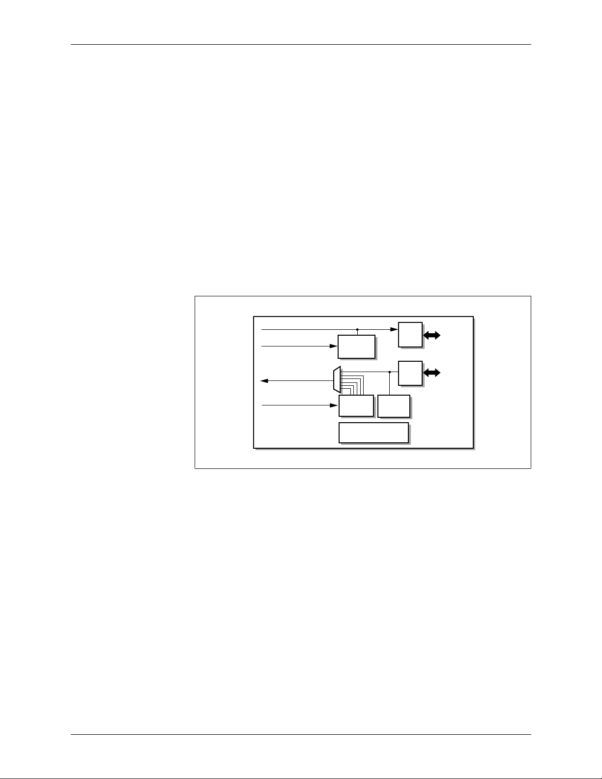
Figure 1-1 illustrates the CX28395 Functional Block Diagram (single framer).
Figure 1-1. CX28395 Functional Block Diagram
Receive NRZ Data
Receive NRZ Clock
Transmit NRZ Data
Transmit NRZ Clock
T1/E1
Receive
Framer
Overhead
Insertion
Data Link Controllers
Transmit
DL1 + DL2
T1/E1
Framer
RX
Slip
Buffer
TX
Slip
Buffer
Receive
System
Bus
Transmit
System
Bus
8394-8-5_011
1-2 Conexant 100054E

CX28394/28395/28398 1.0 Product Description
Quad/x16/Octal—T1/E1/J1 Framers
1.2 Pin Assignments
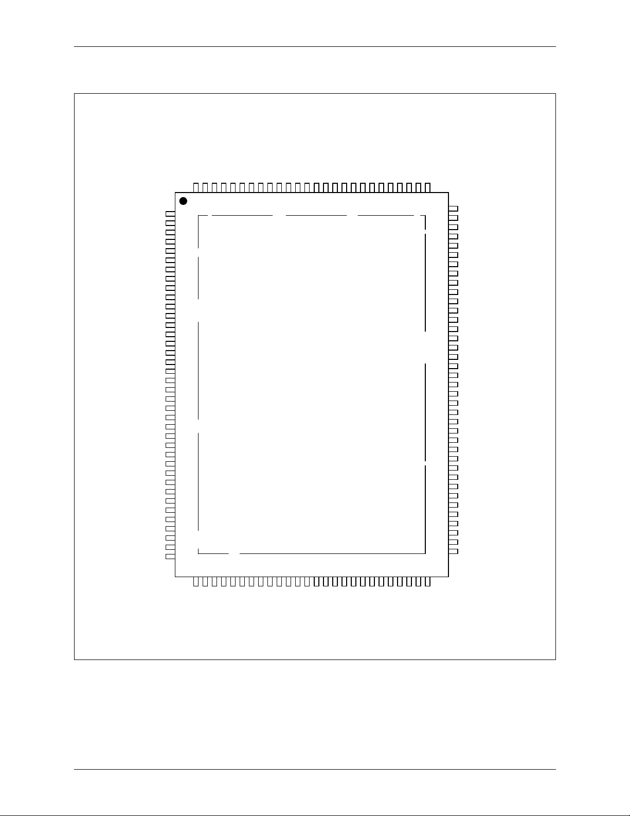
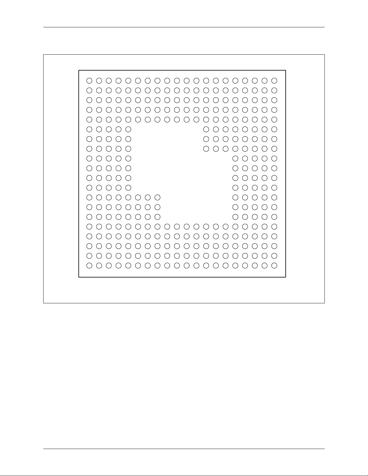
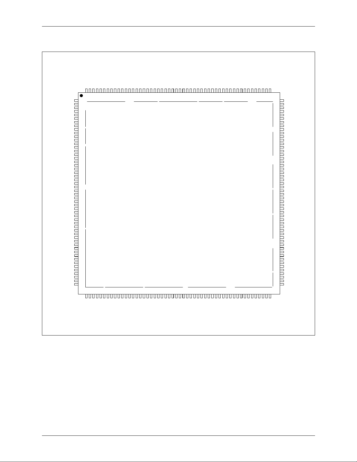
The CX28394 is packaged in a 128-pi n Quad Flat P ac k (TQFP). The CX 28395 is
packaged in a 318-pin Ball Grid Array (BGA) multi-chip module (MCM). The
CX28398 has two package alternatives: a 208-pin Quad Flat Pack (MQFP) and a
272-pin BGA. Pinout diagrams are provided in Figures 1-2 through 1-6 and
Tables 1-1 through 1-4 summarize pin assignments for system bus pins. Table 1-5
lists all other pin assignments.
the hardware signals.
remain unconnected if the active high input state is desired:
A[7:0] Address lines unused in INTEL bus mode.
MOTO* Pullup selects INTEL bus mode if unconnected.
SYNCMD Pullup selects synchronous processor interface.
TDI (CX28394/28398) JTAG unused if not connected.
TDI1, TDI2 (CX28395) JTAG unused if not connected.
TMS JTAG unused if not connected.
TCK Disables JTAG if not connected.
TRST* Disables JTAG reset if not connected.
RST* Disables hardware reset if not connected.
SERDI May be left unconnected if not used.
1.2 Pin Assignments
Figures 1-7 through 1-12 illustrate the devices’ logic, and Table 1-6 defines
The following input pins cont ain an i nt ernal pul lu p r esi sto r ( >50 k
Ω) and may
100054E Conexant 1-3
1.0 Product Description CX28394/28395/28398
1.2 Pin Assignments Quad/x16/Octal—T1/E1/J1 Framers
Figure 1-2. CX28394 128-pin TQFP Pinout Di agram
TNEGO[4] / MSYNCO[4]
TCKI[4]
RCKI[4]
RPOSI[4]
RNEGI[4]
EIACKI
VSS
T1ACKI
VSS
SYSCKI
VSS
VDD
RPCMO[4] / RSIGO[4]
RFSYNC[4] / RMSYNC[4]
RSBCKI[4] / RFSYNC
SIGFRZ[4]
RSIGO[4] / RDLO[4]
RINDO[4] / RDLCKO[4]
TPCMI[4] / TSIGI[4]
TFSYNC[4] / TMSYNC[4]
TSBCKI[4] / TFSYNC
TSIGI[4] / TDLI[4]
TINDO[4] / TDLCKO[4]
VDD
RPCMO[3]/RSIGO[3]
RFSYNC[3] / RMSYNC[3]
RSBCKI[3] / RINDO
SIGFRZ[3]
RSIGO[3] / RDLO[3]
RINDO[3] / RDLCKO[3]
TPCMI[3] / TSIGI[3]
TFSYNC[3] / TMSYNC[3]
TSBCKI[3] / TINDO
TSIGI[3] / TDLI[3]
TINDO[3] / TDLCKO[3]
VGG
VSS
TRST*
RNEGI[3]
TCK0[4]
TPOSO[4] / TNRZO[4]
128
127
125
1
2
3
4
5
6
7
8
9
10
11
12
13
14
15
16
17
18
19
20
21
22
23
24
25
26
27
28
29
30
31
32
33
34
35
36
37
38
126
XMTR3 / RCVR3 XMTR1 / RCVR1
XMTR4 / RCVR4
CLKs
TSB4 / RSB4TSB3 / RSB3
JTAG
39
40434241444546474849505152535455565758596061626364
TPOSO[3] / TNRZO[3]
TNEGO[3] / MSYNCO[3]
VDD
124
123
122
121
120
119
118
XMTR2 / RCVR2
CX28394
117
RNEGI[2]
TCK0[3]
TCKI[3]
RCKI[3]
RPOSI[3]
TPOSO[2] / TNRZO[2]
TNEGO[2] / MSYNCO[2]
116
115
114
113
112
111
110
VDD
RNEGI[1]
TCK0[2]
TCKI[2]
RCKI[2]
RPOSI[2]
TPOSO[1] / TNRZO[1]
TNEGO[1] / MSYNCO[1]
TCKI[1]
RCKI[1]
RPOSI[1]
109
108
107
106
105
SERIO
MPU
SERCS1*
TCK0[1]
104
103
102
101
100
99
98
97
96
95
94
93
92
TSB1 / RSB1
91
90
89
88
87
86
85
84
83
82
81
80
79
TSB2 / RSB2
78
77
76
75
74
73
72
71
70
69
68
67
66
65
SERDI
SERDO
SERCKO
TINDO[1] / TDLCKO[1]
TSIGI[1] / TDLI[1]
TSBCKI[1] / TSBCKI
TFSYNC[1] / TMSYNC[1]
TPCMI[1] / TSIGI[1]
RINDO[1] / RDLCKO[1]
RSIGO[1] / RDLO[1]
SIGFRZ[1]
RSBCKI[1] / RSBCKI
RFSYNC[1] / RMSYNC[1]
RPCMO[1] / RSIGO[1]
VSS
VDD
VSS
TINDO[2] / TDLCKO[2]
TSIGI[2] / TDLI[2]
TSBCKI[2] / TPCMI
TFSYNC[2] / TMSYNC[2]
TPCMI[2] / TSIGI[2]
RINDO[2] / RDLCKO[2]
RSIGO[2] / RDLO[2]
SIGFRZ[2]
RSBCKI[2] / RPCMO
RFSYNC[2] / RMSYNC[2]
RPCMO[2] / RSIGO[2]
AD[0]
AD[1]
AD[2]
AD[3]
AD[4]
AD[5]
AD[6]
AD[7]
VSS
A[0]
TMS
TDI
TDO
TCK
VDD
ONESEC
INTR*
DTACK*
DS* / RD*
R/W* / WR*
CS*
AS* / ALE
MCLK
SYNCMD
RST*
MOTO*
A[9]
A[10]
A[8]
A[7]
A[6]
A[5]
A[4]
A[3]
A[2]
A[1]
8394-8-5_016
1-4 Conexant 100054E
CX28394/28395/28398 1.0 Product Description
Quad/x16/Octal—T1/E1/J1 Framers
Figure 1-3. CX28395 318-pin BGA Pinout Diagram
1 2 3 4 5 6 7 8 9 10111213141516 171819 20
A
B
C
D
E
F
G
H
J
K
L
M
N
P
R
T
U
V
W
Y
Top View
1.2 Pin Assignments
A
B
C
D
E
F
G
H
J
K
L
M
N
P
R
T
U
V
W
Y
1 2 3 4 5 6 7 8 9 10111213141516 171819 20
8394-8-5_013
100054E Conexant 1-5
1.0 Product Description CX28394/28395/28398
1.2 Pin Assignments Quad/x16/Octal—T1/E1/J1 Framers
Figure 1-4. CX28398 208-pin PQFP Pinout Diagram
VGG
VSS
TRST*
TMS
TDO
FSYNC[8] / TMSYNC[8]
TSBCKI[8] / TFSYNC[B]
TINDO[8] / TDLCKO[8]
RPCMO[7] / RSIGO[7]
FSYNC[7] / RMSYNC[7]
RSBCKI[7] / RINDO[B]
RINDO[7] / RDLCKO[7]
FSYNC[7] / TMSYNC[7]
TSBCKI[7] / TINDO[B]
TINDO[7] / TDLCKO[7]
VDD
TSIGI[8] / TDLI[8]
ONESEC
INTR*
DTACK*
R/W* / WR*
DS* / RD*
AS* / ALE
MCLK
SYNCMD
MOTO*
RST*
VSS
SIGFRZ[7]
RSIGO[7] / RDLO[7]
TPCMI[7] / TSIGI[7]
TSIGI[7] / TDLI[7]
A[11]
A[10]
VDD
VSS
AD[7]
AD[6]
AD[5]
TCK
3
VSS
TINDO[3] / TDLCKO[3]
TSIGI[3] / TDLI[3]
TSBCKI[3] / TINDO[A]
TPCMI[3] / TSIGI[3]
RINDO[3] / RDLCKO[3]
RSIGO[3] / RDLO[3]
TFSYNC[3] / TMSYNC[3]
208
206
205
204
203
MPU
MPU
202
55
56
57
58
59
207
1
2
3
4
5
TDI
6
JTAG
7
8
9
10
TSB8 / RSB8
11
12
13
14
15
16
17
CS*
18
19
20
21
22
23
24
25
26
27
28
29
30
31
TSB7 / RSB7
32
33
34
35
36
37
A[9]
38
39
A[8]
A[7]
40
A[6]
41
42
A[5]
43
A[4]
44
A[3]
45
A[2]
A[1]
46
47
A[0]
48
49
50
51
52
53
54
VDD
SIGFRZ[3]
RSBCKI[3] / RINDO[A]
201
200
60
61
TPCMI[8] / TSIGI[8]
RPCMO[3]/RSIGO[3]
RFSYNC[3] / RMSYNC[
199
198
197
196
195
TSB6 / RSB6 TSB5 / RSB5TSB2 / RSB2 TSB1 / RSB1
62
63
64
65
66
8
TINDO[4] / TDLCKO[4]
TSIGI[4] / TDLI[4]
TSBCKI[4] / TFSYNC[A]
TPCMI[4] / TSIGI[4]
TFSYNC[4] / TMSYNC[4]
RINDO[8] / RDLCKO[8]
194
RPCMO[8] / RSIGO[8]
RSIGO[8] / RDLO[8]
SIGFRZ[8]
RSBCKI[8] / RFSYNC[B]
RFSYNC[8] / RMSYNC[
193
192
191
190
189
188
187
186
185
184
TSB8 / RSB8 TSB4 / RSB4TSB3 / RSB3 CLKsXMTR8 / RCVR8 XMTR7 / RCVR7
RINDO[4] / RDLCKO[4]
RSIGO[4] / RDLO[4]
SIGFRZ[4]
RSBCKI[4] / RFSYNC[A]
181
180
183
182
4
RNEGI[8]
RPOSI[8]
RCKI[8]
RPCMO[4] / RSIGO[4]
RFSYNC[4] / RMSYNC[
179
TCKI[8]
178
177
176
175
174
TNEGO[8] / MSYNCO[8]
TPOSO[8] / TNRZO[8]
TCK0[8]
RNEGI[7]
RPOSI[7]
RCKI[7]
TCKI[7]
173
172
171
170
169
168
167
CX28398
67
68
69
70
71
72
73
74
75
76
77
78
79
80
81
82
83
84
85
86
87
88
89
90
91
92
93
94
TNEGO[7] / MSYNCO[7]
TPOSO[7] / TNRZO[7]
TCK0[7]
VDD
VSS
SYSCKI
166
165
164
163
162
161
XMTR4 / RCVR4
XMTR3 / RCVR3
XMTR6 / RCVR6
XMTR2 / RCVR2
XMTR5 / RCVR5
XMTR1 / RCVR1
95
96
97
98
99
100
VSS
160
101
T1ACKI
159
SERIO
102
VSS
158
103
EIACKI
157
156
155
154
153
152
151
150
149
148
147
146
145
144
143
142
141
140
139
138
137
136
135
134
133
132
131
130
129
128
127
126
125
124
123
122
121
120
119
118
117
116
115
114
113
112
111
110
109
108
107
106
105
104
RNEGI[4]
RPOSI[4]
RCKI[4]
TCKI[4]
TNEGO[4] / MSYNCO
TPOSO[4] / TNRZO[4]
TCK0[4]
VDD
RNEGI[3]
RPOSI[3]
RCKI[3]
TCKI[3]
TNEGO[3] / MSYNCO
TPOSO[3] / TNRZO[3
TCK0[3]
VDD
VSS
RNEGI[6]
RPOSI[6]
RCKI[6]
TCKI[6]
TNEGO[6] / MSYNCO
TPOSO[6] / TNRZO[6
TCK0[6]
RNEGI[2]
RPOSI[2]
RCKI[2]
TCKI[2]
TNEGO[2] / MSYNCO
TPOSO[2] / TNRZO[2
TCK0[2]
RNEGI[5]
RPOSI[5]
RCKI[5]
TCKI[5]
TNEGO[5] / MSYNCO
TPOSO[5] / TNRZO[5
TCK0[5]
VDD
VSS
RNEGI[1]
RPOSI[1]
RCKI[1]
TCKI[1]
TNEGO[1] / MSYNCO
TPOSO[1] / TNRZO[1
TCK0[1]
SERCS2*
SERCS1*
SERDI
SERDO
SERCKO
]
]
]
]
]
TSIGI[5] / TDLI[5]
TSBCKI[5] / TSBCKI[B]
TFSYNC[5] / TMSYNC[5]
VDD
VSS
TINDO[5] / TDLCKO[5]
SIGFRZ[1]
RSIGO[1] / RDLO[1]
RPCMO[1] / RSIGO[1]
RINDO[1] / RDLCKO[1]
RSBCKI[1] / RSBCKI[A]
FSYNC[1] / RMSYNC[1]
R
TPCMI[1] / TSIGI[1]
TFSYNC[1] / TMSYNC[1]
TSIGI[1] / TDLI[1]
TSBCKI[1] / TSBCKI[A]
TINDO[1] / TDLCKO[1]
8394-8-5_023
AD[4]
AD[3]
AD[2]
AD[1]
AD[0]
RPCMO[6] / RSIGO[6]
FSYNC[6] / RMSYNC[6]
R
SIGFRZ[6]
TPCMI[6] / TSIGI[6]
RSIGO[6] / RDLO[6]
RINDO[6] / RDLCKO[6]
RSBCKI[6] / RPCMO[B]
FSYNC[6] / TMSYNC[6]
T
TSIGI[6] / TDLI[6]
TSBCKI[6] / TPCMI[B]
TINDO[6] / TDLCKO[6]
SIGFRZ[2]
RSIGO[2] / RDLO[2]
RPCMO[2] / RSIGO[2]
RINDO[2] / RDLCKO[2]
RSBCKI[2] / RPCMO[A]
FSYNC[2] / RMSYNC[2]
R
TPCMI[2] / TSIGI[2]
TFSYNC[2] / TMSYNC[2]
TSIGI[2] / TDLI[2]
TSBCKI[2] / TPCMI[A]
VSS
RPCMO[5] / RSIGO[5]
TINDO[2] / TDLCKO[2]
FSYNC[5] / RMSYNC[5]
R
SIGFRZ[5]
TPCMI[5] / TSIGI[5]
RSIGO[5] / RDLO[5]
RINDO[5] / RDLCKO[5]
RSBCKI[5] / RSBCKI[B]
1-6 Conexant 100054E

CX28394/28395/28398 1.0 Product Description
Quad/x16/Octal—T1/E1/J1 Framers
Figure 1-5. CX28398 208-pin CABGA Pinout Diagram
23456789101112131415161 17
A
B
C
D
E
F
G
H
J
Top View
1.2 Pin Assignments
A
B
C
D
E
F
G
H
J
K
L
M
N
P
R
T
U
23456789101112131415161 17
K
L
M
N
P
R
T
U
100054_001
100054E Conexant 1-7
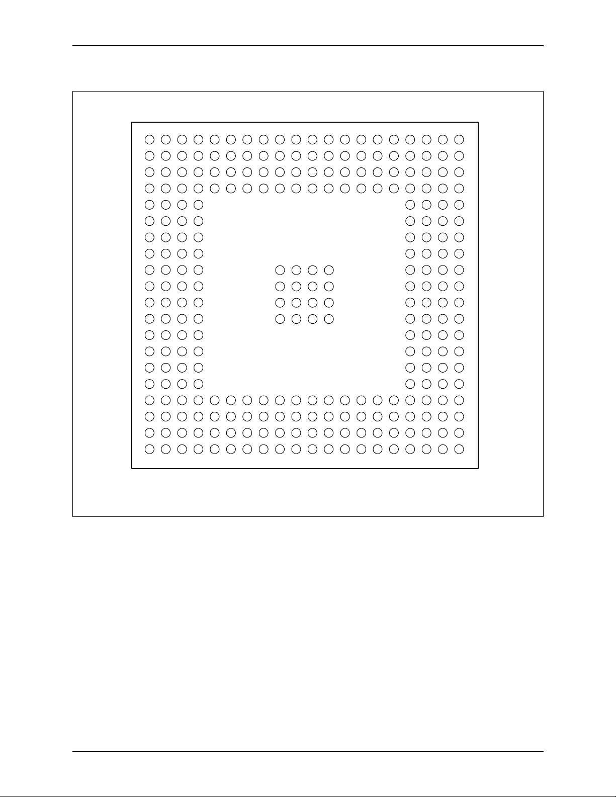
1.0 Product Description CX28394/28395/28398
1.2 Pin Assignments Quad/x16/Octal—T1/E1/J1 Framers
Figure 1-6. CX28398 272-pin BGA Pinout Diagram
1 2 3 4 5 6 7 8 9 10111213141516 171819 20
A
B
C
D
E
F
G
H
J
K
L
M
N
P
R
T
U
V
W
Y
Top View
A
B
C
D
E
F
G
H
J
K
L
M
N
P
R
T
U
V
W
Y
1 2 3 4 5 6 7 8 9 10111213141516 171819 20
8394-8-5_005
1-8 Conexant 100054E

CX28394/28395/28398 1.0 Product Description
Quad/x16/Octal—T1/E1/J1 Framers
Table 1-1. Pin Assignments (SBI1, SBI2, SBI3, SBI4) (1 of 2)
Pin Number System Bus Interface Pin Functions
Non-Multiplexed Mode
CX28394
89 94 R12 V15 J3 RPCMO[1] RSIGO[1]
90 95 P11 W16 J4 RFSYNC[1]/RMSYNC[1] RMSYNC[1]
91 96 U14 Y17 J2 RSBCKI[1] RSBCKI[A]
92 97 T14 V16 — SIGFRZ[1] SIGFRZ[1]
93 98 R13 W17 — RSIGO[1] / RDLO[1] RDLO [ 1]
————J1RSIGO[1] TSTO[1]
94 99 P12 Y18 — RINDO[1] / RDLCKO[1] RDLCKO[1]
95 100 U15 V17 K4 TPCMI[1] TSIGI[1]
96 101 U16 W18 K1 TFSYNC[1]/TMSYNC[1] TMSYNC[1]
128-pin TQFP
CX28398
208-pin PQFP
CX28398
208-pin CABGA
CX28398
CX28395
272-pin BGA
318-pin BGA
SBIMODE[0] = 0 [FCR; addr 080]
SBIMODE[0] = 1 [FCR; addr 080]
1.2 Pin Assignments
Multiplexed Mode
97 102 R14 Y19 K3 TSBCKI[1] TSBCKI[A]
98 103 P13 V18 — TSIGI[1] / TDLI [1] TDLI[1]
— — — — K2 TSIGI[1] TSTI[1]
99 104 T15 W19 — TINDO[1] / TDLCKO[1] TDLCKO[1]
————K5TINDO[1] —
75 69 R6 W8 E4 RPCMO[2] RSIGO[2]
76 70 T6 Y8 E3 RFSYNC[2]/RMSYNC[2] RMSYNC[2]
77 71 U7 V9 E2 RSBCKI[2] RPCMO[A]
78 72 P7 W9 — SIGFRZ[2] SIGFRZ[2]
79 73 R7 Y9 — RSIGO[2] / RDLO[2] R DLO[2]
————F4RSIGO[2] TSTO[2]
80 74 T7 W10 — RINDO[2] / RDLCKO[2] RDLCKO[2 ]
81 75 U8 V10 F3 TPCMI[2] TSIGI[2]
82 76 P8 Y10 F2 TFSYNC[2]/TMSYNC[2] TMSYNC[2]
83 77 R8 Y11 E1 TSBCKI[2] TPCMI[A]
84 78 T8 W 11 — TSIGI[2] / TDLI[2] TDLI[2]
— — — — F1 TSIGI[2] TSTI[2]
85 79 U9 V11 — TINDO[2] / TDLCKO[2] TDLCKO[2]
— — — — H5 TINDO[2] —
25 198 C6 C6 U9 RPCMO[3] RSIGO[3]
26 199 D6 B5 Y9 RFSYNC[3]/RMSYNC[3] RMSYNC[3]
100054E Conexant 1-9

1.0 Product Description CX28394/28395/28398
1.2 Pin Assignments Quad/x16/Octal—T1/E1/J1 Framers
Table 1-1. Pin Assignments (SBI1, SBI2, SBI3, SBI4) (2 of 2)
Pin Number System Bus Interface Pin Functions
Non-Multiplexed Mode
SBIMODE[0] = 0 [FCR; addr 080]
CX28394
27 200 C5 A4 U10 RSBCKI[3] RINDO[A]
28 201 D5 C5 — SIGFRZ[3] SIGFRZ[3]
29 202 B5 B4 — RSIGO[3] / RDLO[3] RDLO [ 3]
————Y10RSIGO[3] TSTO[3]
30 203 A4 A3 — RINDO[3] / RDLCKO[3] RDLCKO[3]
31204A3C4V9TPCMI[3] TSIGI[3]
32 205 B3 B3 W10 TFSYNC[3]/TMSYNC[3] TMSYNC[3]
33 206 C4 B2 V10 TSBCKI[3] TINDO[A]
34 207 A2 A2 — TSIGI[3] / TDLI[3] TDLI[3]
— — — — W9 TSIGI[3] TSTI[3]
35 208 B4 C3 — TINDO[3] / TDLCK O[ 3] TDLCKO[3]
————T10TINDO[3] —
13 178 A11 B11 U5 RPCMO[4] RSIGO[4]
14 179 B10 C11 W5 RFSYNC[4]/RMSYNC[4] RMSYNC[4]
CX28398
128-pin TQFP
208-pin PQFP
CX28398
CX28398
208-pin CABG A
CX28395
272-pin BGA
318-pin BGA
Multiplexed Mode
SBIMODE[0] = 1 [FCR; addr 080]
15 180 C10 A11 V6 RSBCKI[4] RFSYNC[A]
16 181 D10 A10 — SIGFRZ[4] SIGFRZ[4]
17 182 A10 B10 — RSIGO[4] / RDLO[4] RDLO[4]
————Y5RSIGO[4] TSTO[4]
18 183 A9 C10 — RINDO[4] / RDLCKO[4] RDLCKO[4]
19 184 B9 A9 W6 TPCMI[4] TSIGI[4]
20 185 C9 B9 V5 TFSYNC[4]/TMSYNC[4] TMSYNC[4]
21 186 D9 C9 U6 TSBCKI[4] TFSYNC[A]
22 187 A8 A8 — TSIGI[4] / TDLI[4] TDLI[4]
— — — — Y6 TSIGI[4] TSTI[4]
23 188 C8 B8 — TINDO[4] / TDLCK O[ 4] TDLCKO[4]
————T8TINDO[4] —
1-10 Conexant 100054E

CX28394/28395/28398 1.0 Product Description
Quad/x16/Octal—T1/E1/J1 Framers
Table 1-2. Pin Assignments (SBI5, SBI6, SBI7, SBI8) (1 of 2)
Pin Number System Bus Interface Pin Functions Pin Functions
Non-Multiplexed Mode
CX28394
— 81 U10 Y12 G4 RPCMO[5] RSIGO[5]
— 82 R9 W12 G2 RFSYNC[5] / RMSYNC[5] RMSYNC[5]
— 83 P9 V12 G3 RSBCKI[5] RSBCKI[B]
— 84 T10 Y13 — SIGFRZ[5] SIGFRZ[5]
— 85 R10 W13 — RSIGO[5] / RDLO[5] RDLO [5]
————G1RSIGO[5] TSTO[5]
— 86 U11 V13 — RINDO[5] / RDLCKO[5] RDLCKO[5]
— 87 T11 Y14 H3 TPCMI[5] TSIGI[5]
— 88 R11 W14 H4 TFSYNC[5] / TMSYNC[5] TMSYNC[5]
128-pin TQFP
CX28398
208-pin PQFP
CX28398
208-pin CABGA
CX28398
CX28395
272-pin BGA
318-pin BGA
SBIMODE[0] = 0 [FCR; addr 080]
SBIMODE[0] = 1 [FCR; addr 080]
1.2 Pin Assignments
Multiplexed Mode
— 89 T12 Y15 H1 TSBCKI[5] TSBCKI[B]
— 90 U12 V14 — TSIGI[5] / TDLI[5] TDLI[5]
— — — — H2 TSIGI[5] TSTI[5]
— 91 P10 W15 — TINDO[5] / TDLCKO[5] TDLCK O[ 5]
————J5TINDO[5] —
—58P4Y4C2RPCMO[6] RSIGO[6]
— 59 U3 V5 C4 RFSYNC[6] / RMSYNC[6] RMSYNC[6]
— 60 U4 W5 C1 RSBCKI[6] RPCMO[B]
— 61 R4 Y5 — SIGFRZ[6] SIGFRZ[6]
— 62 T4 V6 — RSIGO[6] / RDLO[6] RDLO[ 6]
————D4RSIGO[6] TSTO[6]
— 63 U5 W6 — RINDO[6] / RDLCKO[6] RDLCKO[6 ]
— 64 P5 Y6 D2 TPCMI[6] TSIGI[6]
— 65 R5 V7 D3 TFSYNC[6] / TMSYNC[6] TMSYNC[6]
— 66 T5 W7 D1 TSBCKI[6] TPCMI[B]
— 67 U6 Y 7 — TS IGI[6] / TDLI[6] TDLI[6]
— — — — C3 TSIGI[6] TSTI[6]
— 68 P6 V8 — TI NDO[6] / TDLCKO[6] TDLCKO[6]
— — — — G5 TINDO[6] —
— 25 J4 L1 U12 RPCMO[7] RSIGO[7]
— 26 H2 L2 Y11 RFSYNC[7] / RMSYNC[7] RMSYNC[7]
100054E Conexant 1-11

1.0 Product Description CX28394/28395/28398
1.2 Pin Assignments Quad/x16/Octal—T1/E1/J1 Framers
Table 1-2. Pin Assignments (SBI5, SBI6, SBI7, SBI8) (2 of 2)
Pin Number System Bus Interface Pin Functions Pin Functions
Non-Multiplexed Mode
SBIMODE[0] = 0 [FCR; addr 080]
CX28394
— 27 H1 L3 Y12 RSBCKI[7] RINDO[B]
—28J1M1—SIGFRZ[7] SIGFRZ[7]
— 29 J3 M2 — RSIGO[7] / RDLO[7] RDLO[7]
————W11RSIGO[7] TSTO[7]
— 30 J2 M3 — RINDO[7] / RDLCKO[7] RDLCKO[7]
— 31 K4 N1 W12 TPCMI[7] TSIGI[7]
— 32 K1 N2 V11 TFSYNC[7] / TMSYNC[7] TMSYNC[7]
— 33 K2 N3 V12 TSBCKI[7] TINDO[B]
— 34 L 1 P1 — TSIGI[7] / TDLI[7] TDLI[7]
————U11TSIGI[7] TSTI[7]
— 35 K3 P2 — TI NDO[7] / TDLCKO[7] TDLCKO[7]
————T11TINDO[7] —
— 189 D8 C8 W7 RPCMO[8] RSIGO[8]
— 190 B8 A7 V7 RFSYNC[8] / RMSYNC[8] RMSYNC[8]
CX28398
128-pin TQFP
208-pin PQFP
CX28398
CX28398
208-pin CABG A
CX28395
272-pin BGA
318-pin BGA
Multiplexed Mode
SBIMODE[0] = 1 [FCR; addr 080]
— 191 C7 B7 Y7 RSBCKI[8] RFSYNC[B]
— 192 A7 A6 — SIGFRZ[8] SIGFRZ[8]
— 193 D7 C7 — RSIGO[8] / RDLO[8] RDLO[8]
————V8RSIGO[8] TSTO[8]
— 194 B7 B6 — RINDO[8] / RDLCKO[8] RDLCKO[8]
— 195 A6 A5 Y8 TPCMI[8] TSIGI[8]
— 9 E4 E1 W8 TFSYNC[8] / TMSYNC[8] TMSYNC[8]
— 10 E3 F3 U8 TSBCKI[8] TFSYNC[B]
— 11 D2 F2 — TSIGI[8] / TDLI[8] TDLI[8]
— — — — U7 TSIGI[8] TSTI[8]
— 12 D1 F1 — TINDO[ 8] / TDLCKO[8] TDLCKO[8]
————T9TINDO[8] —
1-12 Conexant 100054E
 Loading...