

CONEX CX28332-3x, CX28332-1x, CX28331-3x, CX28331-1x, CX28333-3x Datasheet
...
Advance Information
This document contains information on a product under development. The parametric information
contains target para me te rs that are subject to change.
CX28331/CX28332/CX28333
Single/Dual/Triple E3/DS3/STS-1 Line Interface Unit
The CX28333 is a three-channel, E3/DS3/STS-1 fully-integrated Line Interface Unit
(LIU). It is configured via external pins and does not need a microprocessor interface.
Each channel has an independent equalizer on the receive side requiring no user
configuration. Also, each channel has a programmable transmit pulse shaper that can
be set to ensure that the cross-connect pulse mask requirement is met for transmit
cable length up to 450 feet. The CX28332 is a dual-channel, and the CX28331 is a
single-channel LIU with performance identical to the CX28333.
The CX28333 gives the user new economies of scale in concentrator applications
where three DS3 or STS-1 channels are concentrated into a single STS-3 channel. By
including three independent transceivers on a chip, significant external compo nents are
eliminated, with the exception of 1:1 coupling transformers, termination resistors, and
supply bypass capacitors.
NOTE: In this document, "i" is used to represent the number of channels:
i = 1 (CX28331), i = 2 (CX28332), and i = 3 (CX28333).
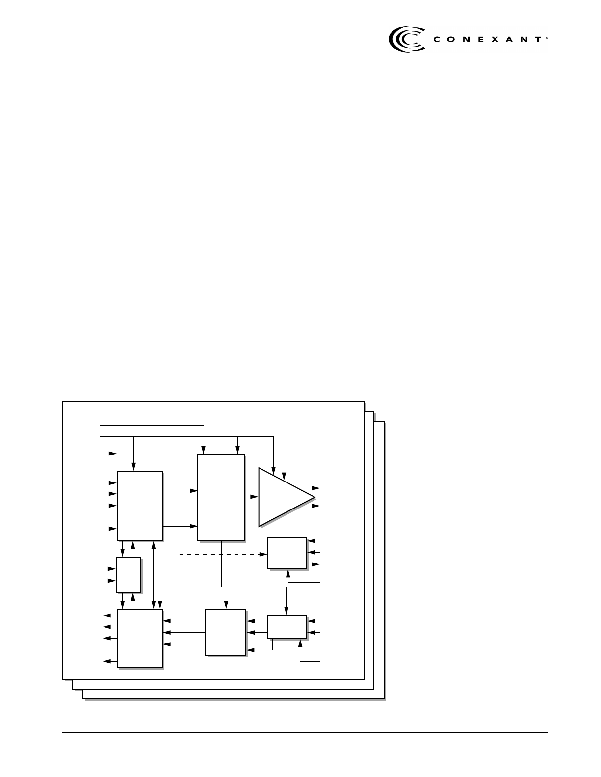
Functional Block Diagram
XOE
LBO
E3MODE
PDB
TPOS
TNEG
TCLK
TAIS
RLOOP
LLOOP
RPOS
RNEG
RCLK
RLOS
NOTE(S):
PDATA/
NDATA
ENCODER
TCLK
DATA
MUX
ENDECDIS
PDATA
NDATA
DECODER
The TX Monitor is only used with the 100-pin CX2833i-3X.
DATCLK
Pulse
Shaper
Clock/
Data
Recovery
DRIVER
P
N
ALOS
LINE
TX
Monitor
Receiver
TLINEP
TLINEM/N
TMONP
TMONM
TXMON
TMONTST
REFCLK
RLINEP
RLINEM/N
REQH
LIU #1
LIU #2
LIU #3
Distinguishing Features
• Can be used as a data transceiver
over a maximum of 900 feet of Type
734/728 coaxial cab le or equivalent
in an on-premise environment
• Programmable pulse filtering to meet
cross-connect pulse masks (ANSI
T1.102-1993)
• Meets jitter specifications of Bellcore
GR499, GR253, and TBR24 (with
external JAT).
• Large input dynamic range
• Alarms for coding violation and loss
of signal
• Full diagnostic loop back capability
• Uses a minimum of external
components
• Compatible with ITU-T G.703, G.823
• Independent power down mode per
channel
• Easily interfaced to the DS3/ E3
Framer IC (CX28342/3/4/6/8 and
CN8330)
• Selectable B3ZS/HDB3
encoding/decoding
• Superior inpu t rec ei v er sensitivity
(< 25 mV)
• Transmit monitor inputs (CX2833i-3x
series only)
Physical Characteristics
• 80- and 100-pin ETQFP package
• Single 3.3 V power supply
• 1 W maximum power dissipation
(CX28333)
• –40 °C to +85 °C temperature range
• 5 V-tolerant pi ns
• TTL digital pins
Applications
• Digital Cross-Connect Syst ems
•Routers
• ATM Switches
• Channelized Line Aggregation Units
• Test Equi pm e nt
• Channel Service Units
• Multiplexers
Data Sheet 100985A
June 2, 2000
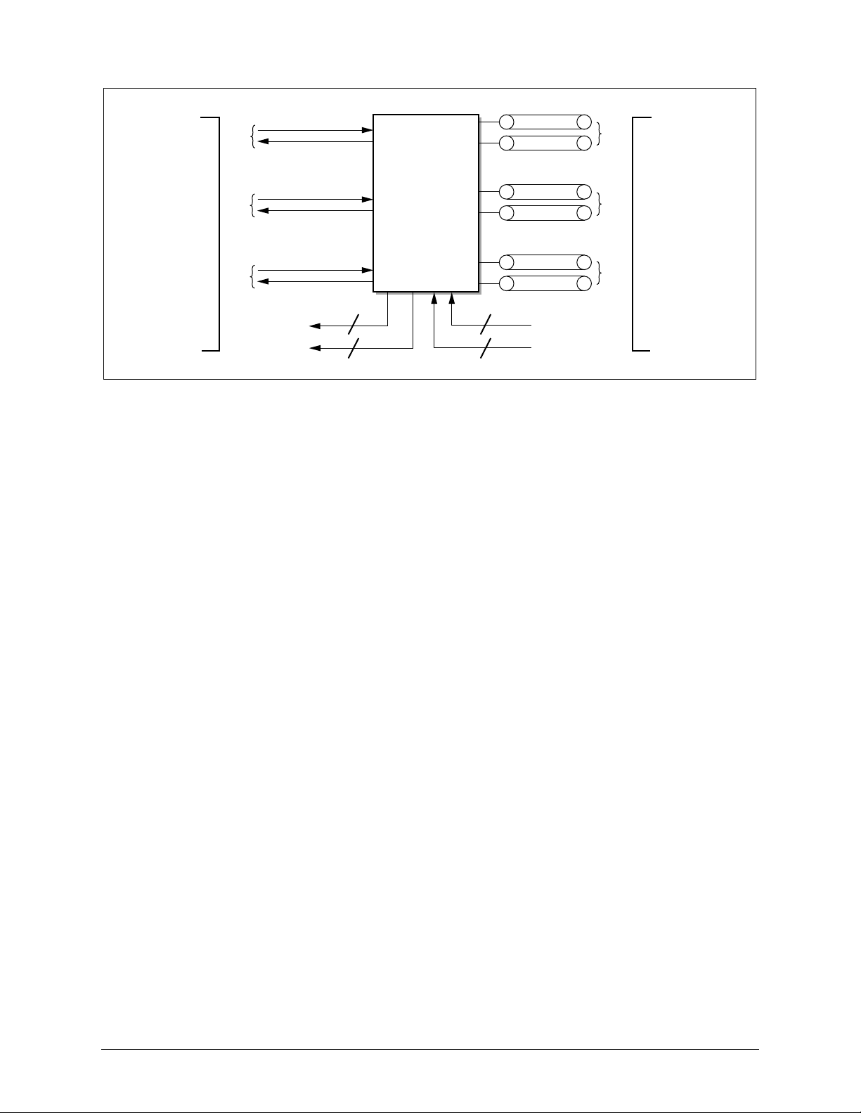
CX28333EVM
NRZTX DATA and CLK in
CH1
NRZRX DATA and CLK out
F
R
NRZTX DATA and CLK in
A
CH2
M
E
NRZRX DATA and CLK out
R
S
NRZTX DATA and CLK in
I
CH3
D
E
NRZRX DATA and CLK out
Loss of Signal
Code Violation
CX28333
TX B3ZS/HDB3 analog out
CH1
RX B3ZS/HDB3 analog in
TX B3ZS/HDB3 analog out
CH2
RX B3ZS/HDB3 analog in
TX B3ZS/HDB3 analog out
CH3
RX B3ZS/HDB3 analog in
Clock Input
Control
L
I
N
E
S
I
D
E
100985_002
© 2000, Conexant Systems, Inc.
All Rights Reserved.
Information in this document is provided in connection with Conexant Systems, Inc. (“Conexant”) products. These materials are
provided by Conexant as a service to its customers and may be used for informational purposes only. Conexant assumes no
responsibility for errors or omissions in these materials. Conexant may make changes to specifications and product descriptions at
any time, without notice. Conexant makes no commitment to update the information and shall have no responsibility whatsoever for
conflicts or incompatibilities arising from future changes to its specifications and product descriptions.
No license, express or implied, by estoppel or otherwise, to any intellectual property rights is granted by this document. Except as
provided in Conexant’s Terms and Conditions of Sale for such products, Conexant assumes no liability whatsoever.
THESE MATERIALS ARE PROVIDED “AS IS” WITHOUT WARRANTY OF ANY KIND, EITHER EXPRESS OR IMPLIED, RELATING
TO SALE AND/OR USE OF CONEXANT PRODUCTS INCLUDING LIABILITY OR WARRANTIES RELATING TO FITNESS FOR A
PARTICULAR PURPOSE, CONSEQUENTIAL OR INCIDENTAL DAMAGES, MERCHANTABILITY, OR INFRINGEMENT OF ANY
PATENT, COPYRIGHT OR OTHER INTELLECTUAL PROPERT Y RIGHT. CONEXANT FURTHER DOES NOT WARRANT THE
ACCURACY OR COMPLETENESS OF THE INFORMATION, TEXT, GRAPHICS OR OTHER ITEMS CONTAINED WITHIN THESE
MATERIALS. CONEXANT SHALL NOT BE LIABLE FOR ANY SPECIAL, INDIRECT, INCIDENTAL, OR CONSEQUENTIAL
DAMAGES, INCLUDING WITHOUT LIMITATION, LOST REVENUES OR LOST PROFITS, WHICH MAY RESULT FROM THE USE
OF THESE MATERIALS.
Conexant products are not intended for use in medical, lifesaving or life sustaining applications. Conexant customers using or selling
Conexant products for use in such applications do so at their own risk and agree to fully indemnify Conexant for any damages
resulting from such improper use or sale.
The following are trademarks of Conexant Systems, Inc.: Conexant™, the Conexant C symbol, and “What’s Next in Communications
Technologies”™. Product names or services listed in this publication are for identification purposes only, and may be trademarks of
third parties. Third-party brands and names are the property of their respective owners.
For additional disclaimer information, please consult Conexant’s Legal Information posted at www.conexant.com, which is
incorporated by reference.
Reader Response: Conexant strives to produce quality documentation and welcomes your feedback. Please send comments and
suggestions to tech.pubs@conexant.com. For technical questions, contact your local Conexant sales off i ce or field applications
engineer.
100985A Conexant

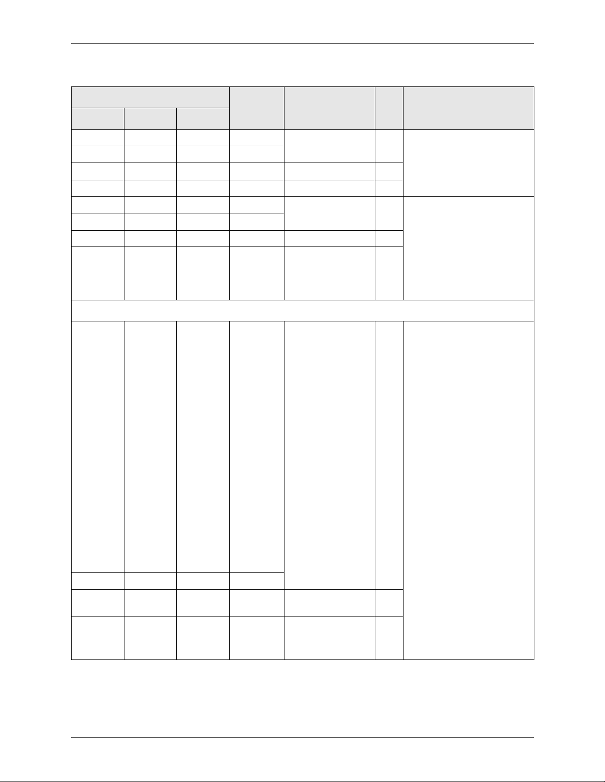
Ordering Information
Model Number Package Description
CX28331-1x 80-Pin ETQFP Single-channel LIU
CX28332-1x 80-Pin ETQFP Dual-channel LIU
CX28333-1x 80-Pin ETQFP Triple-channel LIU
CX28331-3x 100-Pin ETQFP Single channel with Transmit Monitoring
CX28332-3x 100 -Pin ETQFP Dual channel with Transmit Monitoring
CX28333-3x 100-Pin ETQFP Triple channel with Transmit Monitoring
Revision History
Revision Level Date Description
A — May 5, 2000 Initial Release
Operating
Temperature
–40 °C to +85 °C
–40 °C to +85 °C
–40 °C to +85 °C
–40 °C to +85 °C
–40 °C to +85 °C
–40 °C to +85 °C
100985A Conexant

100985A Conexant

Table of Contents
List of Figures . . . . . . . . . . . . . . . . . . . . . . . . . . . . . . . . . . . . . . . . . . . . . . . . . . . . . . . . . . . . . . . . . . . . . . . . vii
List of Tables . . . . . . . . . . . . . . . . . . . . . . . . . . . . . . . . . . . . . . . . . . . . . . . . . . . . . . . . . . . . . . . . . . . . . . . . . . ix
1.0 Pin Description. . . . . . . . . . . . . . . . . . . . . . . . . . . . . . . . . . . . . . . . . . . . . . . . . . . . . . . . . . . . . . . . .1-1
1.1 Pin Assignments. . . . . . . . . . . . . . . . . . . . . . . . . . . . . . . . . . . . . . . . . . . . . . . . . . . . . . . . . . . . 1-1
2.0 Functional Description. . . . . . . . . . . . . . . . . . . . . . . . . . . . . . . . . . . . . . . . . . . . . . . . . . . . . . . . . . 2-1
2.1 Overview. . . . . . . . . . . . . . . . . . . . . . . . . . . . . . . . . . . . . . . . . . . . . . . . . . . . . . . . . . . . . . . . . . 2-1
2.2 Transmitter . . . . . . . . . . . . . . . . . . . . . . . . . . . . . . . . . . . . . . . . . . . . . . . . . . . . . . . . . . . . . . . . 2-3
2.2.1 AMI B3ZS/HDB 3 Encoder . . . . . . . . . . . . . . . . . . . . . . . . . . . . . . . . . . . . . . . . . . . . . . . . 2-3
2.2.2 Pulse Shaper . . . . . . . . . . . . . . . . . . . . . . . . . . . . . . . . . . . . . . . . . . . . . . . . . . . . . . . . . 2-3
2.2.3 Line Driver. . . . . . . . . . . . . . . . . . . . . . . . . . . . . . . . . . . . . . . . . . . . . . . . . . . . . . . . . . . 2-4
2.2.3.1 Transmit Pulse Mask Templates. . . . . . . . . . . . . . . . . . . . . . . . . . . . . . . . . . . 2-5
2.2.4 Alarm Indication Signal (AIS) Ge nerator . . . . . . . . . . . . . . . . . . . . . . . . . . . . . . . . . . . . . 2-8
2.2.5 Transmit Monitor Block (CX2833i-3x Only) . . . . . . . . . . . . . . . . . . . . . . . . . . . . . . . . . . . 2-8
2.2.6 Jitter Generation (Intrinsic). . . . . . . . . . . . . . . . . . . . . . . . . . . . . . . . . . . . . . . . . . . . . . . 2-9
2.3 Receiver . . . . . . . . . . . . . . . . . . . . . . . . . . . . . . . . . . . . . . . . . . . . . . . . . . . . . . . . . . . . . . . . . 2-10
2.3.1 Receive Sensitivity. . . . . . . . . . . . . . . . . . . . . . . . . . . . . . . . . . . . . . . . . . . . . . . . . . . . 2-10
2.3.2 AGC/VGA Block . . . . . . . . . . . . . . . . . . . . . . . . . . . . . . . . . . . . . . . . . . . . . . . . . . . . . . 2-10
2.3.3 Receive Equalizer. . . . . . . . . . . . . . . . . . . . . . . . . . . . . . . . . . . . . . . . . . . . . . . . . . . . . 2-10
2.3.4 The PLL Clock Recovery Circuit . . . . . . . . . . . . . . . . . . . . . . . . . . . . . . . . . . . . . . . . . . 2-11
2.3.5 Loss Of Signal (LOS) Detector . . . . . . . . . . . . . . . . . . . . . . . . . . . . . . . . . . . . . . . . . . . 2-11
2.3.6 B3ZS/HDB3 Decoder With Bipolar Violation Detector. . . . . . . . . . . . . . . . . . . . . . . . . . . 2-11
2.3.7 Data Squelching. . . . . . . . . . . . . . . . . . . . . . . . . . . . . . . . . . . . . . . . . . . . . . . . . . . . . . 2-12
2.4 Jitter Tolerance. . . . . . . . . . . . . . . . . . . . . . . . . . . . . . . . . . . . . . . . . . . . . . . . . . . . . . . . . . . . 2-13
2.4.1 Jitter Transfer. . . . . . . . . . . . . . . . . . . . . . . . . . . . . . . . . . . . . . . . . . . . . . . . . . . . . . . . 2-15
2.5 Additional CX28331/CX28332/CX28333 Functions. . . . . . . . . . . . . . . . . . . . . . . . . . . . . . . . . . 2-16
2.5.1 Bias Generator. . . . . . . . . . . . . . . . . . . . . . . . . . . . . . . . . . . . . . . . . . . . . . . . . . . . . . . 2-16
2.5.2 Power-On Reset (POR). . . . . . . . . . . . . . . . . . . . . . . . . . . . . . . . . . . . . . . . . . . . . . . . . 2-16
2.5.3 Loopback Multiplexers (MUXes). . . . . . . . . . . . . . . . . . . . . . . . . . . . . . . . . . . . . . . . . . 2-16
2.6 Mechanical Specifications . . . . . . . . . . . . . . . . . . . . . . . . . . . . . . . . . . . . . . . . . . . . . . . . . . . 2-17
2.7 Electrical Characteristics . . . . . . . . . . . . . . . . . . . . . . . . . . . . . . . . . . . . . . . . . . . . . . . . . . . . 2-19
100985A Conexant v

Table of Contents CX28331/CX28332/CX28333
Single/Dual/Triple E3/DS3/STS-1 Line Interface Unit
2.7.1 Absolute Maximum Ratings . . . . . . . . . . . . . . . . . . . . . . . . . . . . . . . . . . . . . . . . . . . . . 2-19
2.7.2 Recommended Operating Conditions . . . . . . . . . . . . . . . . . . . . . . . . . . . . . . . . . . . . . . 2-20
2.8 DC Characteristics . . . . . . . . . . . . . . . . . . . . . . . . . . . . . . . . . . . . . . . . . . . . . . . . . . . . . . . . . 2-21
2.9 AC Characteristics. . . . . . . . . . . . . . . . . . . . . . . . . . . . . . . . . . . . . . . . . . . . . . . . . . . . . . . . . . 2-22
3.0 Applications . . . . . . . . . . . . . . . . . . . . . . . . . . . . . . . . . . . . . . . . . . . . . . . . . . . . . . . . . . . . . . . . . . . 3-1
3.1 PCB Design Considerations for CX28331/CX28332/CX28333 . . . . . . . . . . . . . . . . . . . . . . . . . . . 3-1
3.1.1 Power Sup ply and Grou nd Plane. . . . . . . . . . . . . . . . . . . . . . . . . . . . . . . . . . . . . . . . . . . 3-1
3.1.2 Impedance Matching . . . . . . . . . . . . . . . . . . . . . . . . . . . . . . . . . . . . . . . . . . . . . . . . . . . 3-2
3.1.3 Other Passive Parts . . . . . . . . . . . . . . . . . . . . . . . . . . . . . . . . . . . . . . . . . . . . . . . . . . . . 3-2
3.1.4 IBIS Models. . . . . . . . . . . . . . . . . . . . . . . . . . . . . . . . . . . . . . . . . . . . . . . . . . . . . . . . . . 3-2
3.1.5 Recommended Vendors. . . . . . . . . . . . . . . . . . . . . . . . . . . . . . . . . . . . . . . . . . . . . . . . . 3-2
Appendix A . . . . . . . . . . . . . . . . . . . . . . . . . . . . . . . . . . . . . . . . . . . . . . . . . . . . . . . . . . . . . . . . . . . . . . . . . . A-1
A.1 Applicable Standards . . . . . . . . . . . . . . . . . . . . . . . . . . . . . . . . . . . . . . . . . . . . . . . . . . . . . . . . A-1
Appendix B . . . . . . . . . . . . . . . . . . . . . . . . . . . . . . . . . . . . . . . . . . . . . . . . . . . . . . . . . . . . . . . . . . . . . . . . . . B-1
B.1 Evaluation Module Schematic. . . . . . . . . . . . . . . . . . . . . . . . . . . . . . . . . . . . . . . . . . . . . . . . . . B-1
vi Conexant 100985A

CX28331/CX28332/CX28333 List of Figures
Single/Dual/Triple E3/DS3/STS-1 Line Interface Unit
List of Figures
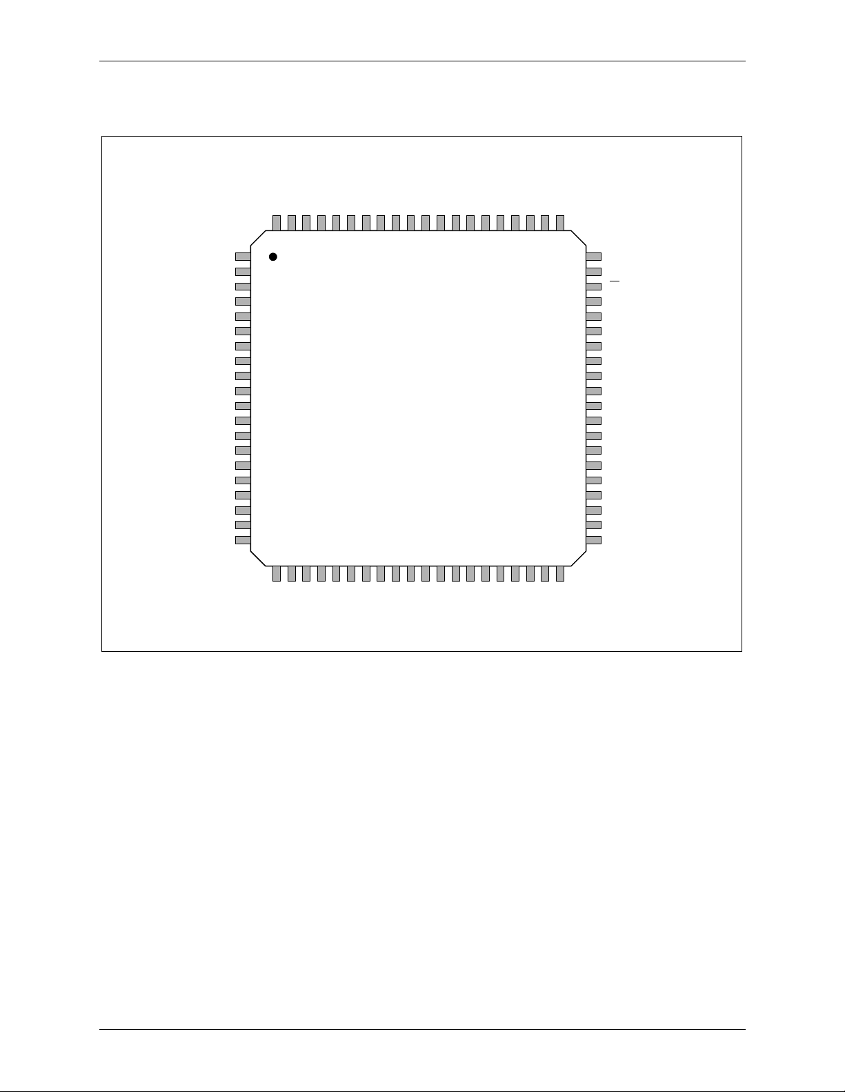
Figure 1-1. CX28331-1x Pin Diagram . . . . . . . . . . . . . . . . . . . . . . . . . . . . . . . . . . . . . . . . . . . . . . . . . . 1-2
Figure 1-2. CX28332-1x Pin Diagram . . . . . . . . . . . . . . . . . . . . . . . . . . . . . . . . . . . . . . . . . . . . . . . . . . 1-3
Figure 1-3. CX28333-1x Pin Diagram . . . . . . . . . . . . . . . . . . . . . . . . . . . . . . . . . . . . . . . . . . . . . . . . . . 1-4
Figure 1-4. CX28331-3x Pin Diagram . . . . . . . . . . . . . . . . . . . . . . . . . . . . . . . . . . . . . . . . . . . . . . . . . 1-11
Figure 1-5. CX28332-3x Pin Diagram . . . . . . . . . . . . . . . . . . . . . . . . . . . . . . . . . . . . . . . . . . . . . . . . . 1-12
Figure 1-6. CX28333-3x Pin Diagram . . . . . . . . . . . . . . . . . . . . . . . . . . . . . . . . . . . . . . . . . . . . . . . . . 1-13
Figure 2-1. Typical Application Of Single CX2833i Channel. . . . . . . . . . . . . . . . . . . . . . . . . . . . . . . . . . 2-2
Figure 2-2. Pulse Shaper. . . . . . . . . . . . . . . . . . . . . . . . . . . . . . . . . . . . . . . . . . . . . . . . . . . . . . . . . . . . 2-3
Figure 2-3. Pulse Measurement Points . . . . . . . . . . . . . . . . . . . . . . . . . . . . . . . . . . . . . . . . . . . . . . . . . 2-4
Figure 2-4. Transmit Pulse Mask for DS3 Rates . . . . . . . . . . . . . . . . . . . . . . . . . . . . . . . . . . . . . . . . . .2-5
Figure 2-5. Transmit Pulse Mask for STS-1 Rates. . . . . . . . . . . . . . . . . . . . . . . . . . . . . . . . . . . . . . . . . 2-6
Figure 2-6. Transmit Pulse Mask for E3 Rate. . . . . . . . . . . . . . . . . . . . . . . . . . . . . . . . . . . . . . . . . . . . . 2 -7
Figure 2-7. AIS Signal . . . . . . . . . . . . . . . . . . . . . . . . . . . . . . . . . . . . . . . . . . . . . . . . . . . . . . . . . . . . . . 2-8
Figure 2-8. Minimum Jitter Tolerance Requirement. . . . . . . . . . . . . . . . . . . . . . . . . . . . . . . . . . . . . . . 2-14
Figure 2-9. Maximum Jitter Transfer Curve Requirement . . . . . . . . . . . . . . . . . . . . . . . . . . . . . . . . . . 2-15
Figure 2-10. CX2833i-1x Mechanical Drawing (80-Pin)—Dimensions . . . . . . . . . . . . . . . . . . . . . . . . . 2-17
Figure 2-11. CX2833i-3x Mechanical Drawing (100-Pin)—Dimensions . . . . . . . . . . . . . . . . . . . . . . . . 2-18
Figure 2-12. Timing Diagram. . . . . . . . . . . . . . . . . . . . . . . . . . . . . . . . . . . . . . . . . . . . . . . . . . . . . . . . . 2-23
Figure 3-1. Typical CX28333 Connection. . . . . . . . . . . . . . . . . . . . . . . . . . . . . . . . . . . . . . . . . . . . . . . . 3-3
Figure B-1. Recommended Schematic for the CX2833i-1x Device . . . . . . . . . . . . . . . . . . . . . . . . . . . . B-2
Figure B-2. Recommended Schematic for the CX2833i-3x Device (1 of 2) . . . . . . . . . . . . . . . . . . . . . . B-3
Figure B-3. Recommended Schematic for the CX2833i-3x Device (2 of 2) . . . . . . . . . . . . . . . . . . . . . . B-4
100985A Conexant vii

List of Figu res CX28331/CX28332/CX28333
Single/Dual/Triple E3/DS3/STS-1 Line Interface Unit
viii Conexant 100985A

CX28331/CX28332/CX28333 List of Tables
Single/Dual/Triple E3/DS3/STS-1 Line Interface Unit
List of Tables
Table 1-1. CX28331/CX28332/CX28333 Pin Definitions . . . . . . . . . . . . . . . . . . . . . . . . . . . . . . . . . . . . 1-5
Table 1-2. CX2833i-3x Pin Definitions. . . . . . . . . . . . . . . . . . . . . . . . . . . . . . . . . . . . . . . . . . . . . . . . . 1-14
Table 2-1. DS3 Transmit Template Specifications . . . . . . . . . . . . . . . . . . . . . . . . . . . . . . . . . . . . . . . . .2-5
Table 2-2. STS-1 Transmit Template Specifications. . . . . . . . . . . . . . . . . . . . . . . . . . . . . . . . . . . . . . . . 2-6
Table 2-3. Absolute Maximum Ratings . . . . . . . . . . . . . . . . . . . . . . . . . . . . . . . . . . . . . . . . . . . . . . . . 2-19
Table 2-4. Recommended Operating Conditions . . . . . . . . . . . . . . . . . . . . . . . . . . . . . . . . . . . . . . . . . 2-20
Table 2-5. DC Characteristics. . . . . . . . . . . . . . . . . . . . . . . . . . . . . . . . . . . . . . . . . . . . . . . . . . . . . . . . 2-21
Table 2-6. AC Characteristics (Logic Timing). . . . . . . . . . . . . . . . . . . . . . . . . . . . . . . . . . . . . . . . . . . . 2-22
100985A Conexant ix

List of Tables CX28331/CX28332/CX28333
Single/Dual/Triple E3/DS3/STS-1 Line Interface Unit
x Conexant 100985A

1
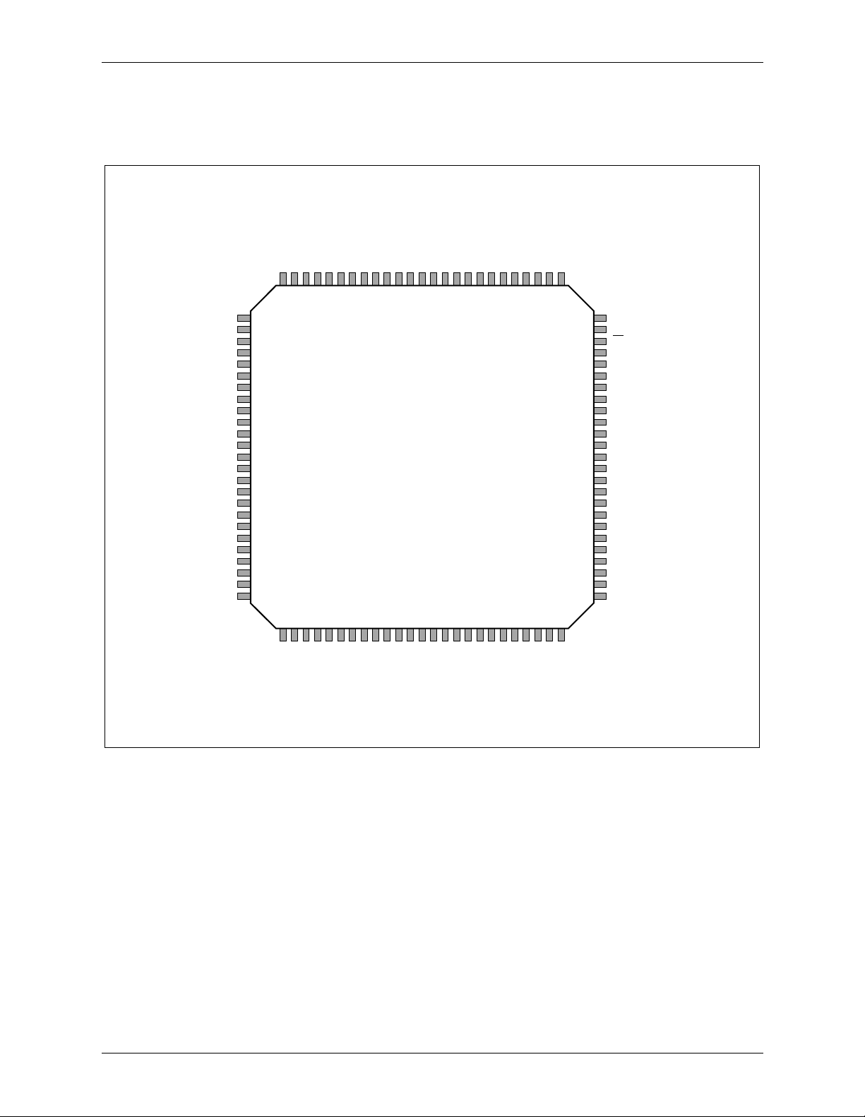
1.0 Pin Description
1.1 Pin Assignments
Figures 1-1 (CX28331-1x), 1-2 (CX28332-1x), and 1-3 (CX28333-1x) illustrate
pin assignments for the 80-pin Exposed Thin Quad Flat Package (ETQFP). See
Table 1-1 for the CX2833i-1x pin descriptions.
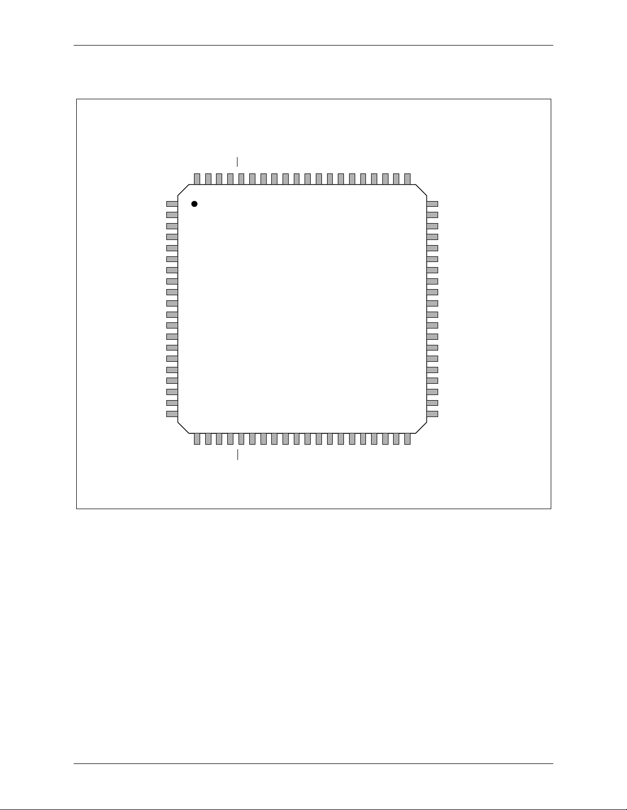
Figures 1-4 (CX28331-3x), 1-5 (CX28332-3x), and 1-6 (CX28333-3x)
illustrate pin assignments for the 100-pin ETQFP. The 100-pin package adds
more functionality, supporting new features such as Tr ansmit Monitoring and
Transmit Monitoring Status testing. See Table 1-2 for the CX2833i-3x pin
descriptions.
The input/output (I/O) column is coded as follows:
I = Input
O = Output
I/O = Bidirectional
P = Power
NOTE: All digital inputs and outputs contain 75 kΩ pull-down resistors.
When a channel is disabled (i.e., the PDx
receive and transmit analog circuitry powers down. Analog inputs (RLINE) are
ignored and analog outputs (TLINE) are high impedance. Digital inputs of a
powered-down channel are still active, but ignored. Overall noise on the device
can be lowered by not driving the digital inputs of a powered-down channel.
NOTE: When power is disconnected from the device, TLINE pins are low
impedance to ground if driven by more than one forward-bias diode
voltage (0.7 V) below ground. Additionally, driving TLINE, a
forward-bias diode voltage above the VGG pin, creates a low impedance
path from the TLINE pin to the VGG pin. Otherwise, the TLINE pins are
high impedance.
pin is tied low or not connected), a ll
100985A Conexant 1-1
1.0 Pin Description CX28331/CX28332/CX28333
1.1 Pin Assignments Single/Dual/Triple E3/DS3/STS-1 Line Interface Unit
Figure 1-1. CX28331-1x Pin Diagram
NC
GPD
RESET
VGG
VSS
NC
NC
VDD
VDD
NC
NC
VSS
TVSS
TLINEP
TLINEN
TVDD
RVDD
RLINEP
RLINEN
RVSS
VSS
NC
NC
VDD
RBIAS
77
78
79
80
1
2
3
4
5
6
7
8
9
10
11
12
13
14
15
16
17
18
19
20
24
23
22
21
NC
NC
76
74
75
25
27
26
NC
NC
DVDDIO
73
CX28331-1x
28
NC
71
72
70
30
29
31
NC
69
32
NC
68
33
NC
NC
66
67
35
34
NC
65
36
NC
64
37
NC
63
38
NC
NC
61
62
40
39
60
59
58
57
56
55
54
53
52
51
50
49
48
47
46
45
44
43
42
41
DVDDC
ENDECDIS
PD
RLOOP
LLOOP
RNEG/RLCV
RPOS/RNRZ
RCLK
RLOS
TAIS
TCLK
TPOS/TNRZ
TNEG/NC
REFCLK
REQH
XOE
LBO
E3MODE
NC
DVSSC
NC
VDD
NC
NC
VSS
NC
NC
NC
NC
DVSSIO
NC
NC
NC
NC
NC
NC
NC
NC
NC
NC
100985_003
1-2 Conexant 100985A
CX28331/CX28332/CX28333 1.0 Pin Description
Single/Dual/Triple E3/DS3/STS-1 Line Interface Unit
Figure 1-2. CX28332-1x Pin Diagram
PD1
GPD
RESET
VGG
TVSS1
TLINE1P
TLINE1N
TVDD1
RVDD1
RLINE1P
RLINE1N
RVSS1
VSS
NC
NC
VDD
VDD
NC
NC
VSS
TVSS2
TLINE2P
TLINE2N
TVDD2
RBIAS
76
77
78
79
80
1
2
3
4
5
6
7
8
9
10
11
12
13
14
15
16
17
18
19
20
25
24
23
22
21
LLOOP1
RLOOP1
74
75
27
26
DVDDIO
73
CX28332-1x
28
LBO1
72
29
XOE1
71
30
REQH1
70
31
RLOS1
RCLK1
RPOS1/RNRZ1
RNEG1/RLCV1
66
67
68
69
35
34
33
32
TNEG1/NC1
REFCLK1
64
65
37
36
TAIS1
TCLK1
TPOS1/TNRZ1
61
62
63
60
59
58
57
56
55
54
53
52
51
50
49
48
47
46
45
44
43
42
41
40
39
38
DVDDC
ENDECDIS
NC
NC
NC
NC
NC
NC
NC
NC
NC
NC
NC
NC
NC
NC
NC
E3MODE
NC
DVSSC
1.1 Pin Assignments
RVDD2
RLINE2P
RVSS2
RLINE2N
PD2
LLOOP2
RLOOP2
LBO2
DVSSIO
XOE2
REQH2
RCLK2
RLOS2
RNEG2/RLCV2
RPOS2/RNRZ2
REFCLK2
TNEG2/NC2
TAIS2
TCLK2
TPOS2/TNRZ2
100985_004
100985A Conexant 1-3

1.0 Pin Description CX28331/CX28332/CX28333
1.1 Pin Assignments Single/Dual/Triple E3/DS3/STS-1 Line Interface Unit
Figure 1-3. CX28333-1x Pin Diagram
PD1
GPD
RESET
VGG
TVSS1
TLINE1P
TLINE1N
TVDD1
RVDD1
RLINE1P
RLINE1N
RVSS1
TVSS2
TLINE2P
TLINE2N
TVDD2
RVDD2
RLINE2P
RLINE2N
RVSS2
TVSS3
TLINE3P
TLINE3N
TVDD3
RBIAS
77
78
79
80
1
2
3
4
5
6
7
8
9
10
11
12
13
14
15
16
17
18
19
20
24
23
22
21
76
25
LLOOP1
RLOOP1
74
75
27
26
XOE1
LBO1
DVDDIO
73
28
REQH1
71
72
70
CX28333-1x
30
29
31
RLOS1
RCLK1
RPOS1/RNRZ1
RNEG1/RLCV1
66
67
68
69
35
34
33
32
TNEG1/NC1
REFCLK1
64
65
37
36
TAIS1
TCLK1
TPOS1/TNRZ1
61
62
63
60
59
58
57
56
55
54
53
52
51
50
49
48
47
46
45
44
43
42
41
40
39
38
DVDDC
ENDECDIS
PD2
RLOOP2
LLOOP2
RNEG2/RLCV2
RPOS2/RNRZ2
RCLK2
RLOS2
TAIS2
TCLK2
TPOS2/TNRZ2
TNEG2/NC2
REFCLK2
REQH2
XOE2
LBO2
E3MODE
NC
DVSSC
RVDD3
RLINE3P
RVSS3
RLINE3N
PD3
LLOOP3
RLOOP3
LBO3
DVSSIO
XOE3
REQH3
RCLK3
RLOS3
RNEG3/RLCV3
RPOS3/RNRZ3
REFCLK3
TNEG3/NC3
TAIS3
TCLK3
TPOS3/TNRZ3
100985_005
1-4 Conexant 100985A

CX28331/CX28332/CX28333 1.0 Pin Description
Single/Dual/Triple E3/DS3/STS-1 Line Interface Unit
Table 1-1. CX2833i-1x Pin Definitions (1 of 6)
Pin #
Signal Name Description I/O/P Notes
CX28331-1x CX28332-1x CX28333-1x
Coaxial Line Pins
14 ——RLINEP Ch1 positive receive
— 66RLINE1P
15 ——RLINEN Ch1 negative receive
— 77RLINE1N
— 22 14 RLINE2P Ch2 positive receive
— 23 15 RLINE2N Ch2 negative receive
——22 RLINE3P Ch3 positive receive
——23 RLINE3N Ch3 negative receive
10 ——TLINEP Ch1 positive transmit
— 2 2 TLINE1P
11 ——TLINEN Ch1 negative transmit
— 33TLINE1N
— 18 10 TLINE2P Ch2 positive transmit
— 19 11 TLINE2N Ch2 negative transmit
data
data
data
data
data
data
data
data
data
data
1.1 Pin Assignments
I Differential inputs for each channel
from its respective receive coax
line. The RX expec ts balanced
differential inputs, usually achieved
I
using a 1:1 transfor mer.
The inputs are inte rnally DC biased
to 1.9 V.
I
I
I
I
O Differential, coax-driver balanced
outputs for pulse-shaped AMI
B3ZS/HDB3 enco ded waveforms
for each channel.
O
These pins should be connected to
the primary side of the 1:1
O
transformer through two
backmatch resistors (see Appendix
O
B).
——18 TLINE3P Ch3 positive transmit
data
——19 TLINE3N Ch3 negative transmit
data
O
O
100985A Conexant 1-5

1.0 Pin Description CX28331/CX28332/CX28333
1.1 Pin Assignments Single/Dual/Triple E3/DS3/STS-1 Line Interface Unit
Table 1-1. CX2833i-1x Pin Definitions (2 of 6)
Pin #
Signal Name Description I/O/P Notes
CX28331-1x CX28332-1x CX28333-1x
Digital Data Pins
54 ——RPOS/
RNRZ
— 68 68 RPOS1/
RNRZ1
55 ——RNEG/
RLCV
— 69 69 RNEG1/
RLCV1
— 33 54 RPOS2/
RNRZ2
— 32 55 RNEG2/
RLCV2
——33 RPOS3/
RNRZ3
——32 RNEG3/
RLCV3
53 ——RCLK Receive clock Ch1 O Recov e red clock for each channel
— 67 67 RCLK1
— 34 53 RCLK2 Receive clock Ch2 O
——34 RCLK3 Receive clock Ch3 O
Ch1 receive Positive rail
or NRZ data
Ch1 receive Negative rail
or line code violation
Ch2 receive Positive rail
or NRZ data
Ch2 receive Negative rail
or line code violation
Ch3 receive Positive rail
or NRZ data
Ch3 receive Negative rail
or line code violation
O Resynchronized receive data
intended to be strobed out by the
corresponding RCLK.
When ENDECDIS = 1, these outputs
are positive and negative AMI data
O
(RPOS and RNEG).
When ENDECDIS = 0, these outputs
are decoded NRZ data (RNRZ) and
line code violation (RLCV). A l ine
O
code violation is in dicated when
RLCV = 1.
O
See notes on the ENDECDIS pin in
O
the Control Signals sect ion.
O
receiver, intended for strobing the
corresponding RDAT into the
following framer or logic.
49 ——TPOS/
TNRZ
— 63 63 TPOS1/
TNRZ1
48 ——TNEG/NCCh1 transmit Negative
— 64 64 TNEG1/
NC1
— 38 49 TPOS2/
TNRZ2
— 37 48 TNEG2/
NC2
——38 TPOS3/
TNRZ3
——37 TNEG3/
NC3
Ch1 transmit Positive
rail or NRZ data
rail or no connect data
Ch2 transmit Positive or
NRZ data
Ch2 transmit Negative
rail or no connect data
Ch3 transmit Positive or
NRZ data
Ch3 transmit Negative
rail or no connect data
I Synchronized transmit data
intended to be strobed in by the
corresponding TCLK.
When ENDECDIS = 1, these inputs
I
are expected to be positive and
negative AMI data (TPOS and
TNEG).
When ENDECDIS = 0, these inputs
I
are expected to be uncoded NRZ
data (TNRZ) and no connects (NC).
I
See notes on the ENDECDIS pin in
the Control Signals sect ion.
I
I
1-6 Conexant 100985A
CX28331/CX28332/CX28333 1.0 Pin Description
Single/Dual/Triple E3/DS3/STS-1 Line Interface Unit
Table 1-1. CX2833i-1x Pin Definitions (3 of 6)
Pin #
Signal Name Description I/O/P Notes
CX28331-1x CX28332-1x CX28333-1x
50 ——TCLK Transmit clock Ch1 I Transmit bit clock input for strobing
— 62 62 TCLK1
— 39 50 TCLK2 T ra ns mit clock Ch2 I
——39 TCLK3 Transm it cl oc k Ch3 I
52 ——RLOS Loss of signal Ch1 O Loss Of Signal (LOS) indication for
— 66 66 RLOS1
— 35 52 RLOS2 Loss of signal Ch2 O
——35 RLOS3 Loss of signal Ch3 O
Control Signals
59 59 59 ENDECDIS Encoder/decoder
disable (for all channels)
51 ——TAIS Transmit Ch1 AIS mode
— 61 61 TAIS1
— 40 51 TAIS2 Transmit Ch2 AIS mode
——40 TAIS3 Transmit Ch3 AIS mode
enable
enable
enable
with transmit data into the CX2833i.
each channel, as determi ned by
insufficient pulse density. Signal
loss detected when RLOS = 1. An
LOS will be asse rte d w h en 175 ±75
0s occur in a row and deasserted
when the pulse density is between
28% and 33% (DS3/STS-1) (i.e., a
1s density).
I 1 = Dual rail pulse coded data
format. Input transmit data pins
TPOS, TNRZ, TNEG and NC are
interpreted as TPOS and TNEG
(encoded positive and negative rail
data). Output receive data pins
RPOS and RNRZ, and RNEG and
RLCV are interpreted as RPOS and
RNEG, with RPO S h a vi ng a positive
pulse in place of every positive AMI
pulse and RNEG havin g a negative
pulse in place of every negative AMI
pulse.
0 = NRZ format. Transmit data pins
TPOS and TNEG are interpreted as
TNRZ and NC (not connected).
Receive data pins RPOS and RNEG
are interpreted as RNRZ and RLCV.
In this mode, all lin e cod e viol ations
are reported as active high on
RLCV.
I Transmission of Alarm Indication
Signal (AIS) for a given chann el.
Replace transmit data with AIS
signal. The AMI form of AIS
I
supported is alternating 1s.
I
(+1, -1, +1, -1, +1, ...)
Looping takes precedence over AIS.
1 = AIS mode enabled
0 = AIS mode disabled
1.1 Pin Assignments
100985A Conexant 1-7

1.0 Pin Description CX28331/CX28332/CX28333
1.1 Pin Assignments Single/Dual/Triple E3/DS3/STS-1 Line Interface Unit
Table 1-1. CX2833i-1x Pin Definitions (4 of 6)
Pin #
Signal Name Description I/O/P Notes
CX28331-1x CX28332-1x CX28333-1x
43 43 43 E3MODE E3MODE I When the pin is set to high, it
enables the E3 mode on al l
channels, in stea d of t he DS 3/S TS-1
mode. This also changes the pulse
shaper to E3 mode and overrides all
LBO pins. It also changes the
encoder/decoder from B3ZS mode
to HDB3 mode.
1 = E3 mode
0 = DS3/STS-1 mode
44 ——LBO Transm it lin e Ch1
— 72 72 LBO1
— 29 44 LBO2 Transmit line Ch2
——29 LBO3 Transmit line Ch3
build-out mode
build-out mode
build-out mode
56 ——LLOOP Local loopback enable
— 74 74 LLOOP1
— 27 56 LLOOP2 Local loopback enable
——27 LLOOP3 Local loopback enable
57 ——RLOOP Remote loopback enable
— 75 75 RLOOP1
— 26 57 RLOOP2 Remote loopback enable
——26 RLOOP3 Remote loopback enable
45 ——XOE Trans m it ou tpu t en able
— 71 71 XOE1
— 30 45 XOE2 Transmit output enable
Ch1
Ch2
Ch3
Ch1
Ch2
Ch3
Ch1
Ch2
I Line build-out mode per ch an ne l,
based on the length of cable on the
transmit side of the cross-connect
block. This bit is overridden and the
I
pulse shaper is disabled (no pulse
shaping) if E3MODE = 1.
I
1 = Inserts line build-out into the
transmit channel. U sually used
when the transmit cable is less than
350 feet in length.
0 = Line build-out bypassed (not
inserted). Usually used when the
transmit cable is grea ter than 350
feet in length.
I Local loopback enable per channel.
The transmit data is l ooped back
immediately from the encoder to
the decoder in place of the received
I
data.
1 = local loopback enabled
I
0 = local loopback disabled
I Remote loopback enable per
channel. The receive data, retimed
after clock recovery, is looped back
into the AMI generator in place of
I
the transmit data.
1 = remote loopback enabled
I
0 = remote loopback disabled
I Transmit output enable per channel.
1 = transmit line output driver
enabled
0 = transmit output driver set to
I
high impedance state
——30 XOE3 Transmit output enable
Ch3
1-8 Conexant 100985A
I

CX28331/CX28332/CX28333 1.0 Pin Description
Single/Dual/Triple E3/DS3/STS-1 Line Interface Unit
Table 1-1. CX2833i-1x Pin Definitions (5 of 6)
Pin #
Signal Name Description I/O/P Notes
CX28331-1x CX28332-1x CX28333-1x
46 ——REQH Ch1 Receive High EQ
— 70 70 REQH1
— 31 46 REQH2 Ch2 Receive High EQ
——31 REQH3 Ch3 Receive High EQ
Gain Enable
Gain Enable
Gain Enable
Power/Ground
1.1 Pin Assignments
I The equalizer in the CX2833i has
two gain settings. The higher gain
setting is designed to optimally
equalize a nominally-shaped (meets
the pulse template), pulse-driven
DS3 or STS-1 wavefor m that is
I
driven through 0–900 feet of cable.
Square-shaped pulses such as E3
or DS3-HIGH require less
high-frequency gain and should use
the low EQ gain setting.
REQH = 1 high EQ gain
(DS3/STS-1 modes)
REQH = 0 low EQ gain (E3/DS3
Square Modes)
(1)
per channel (3.3 V).
per channel.
channel (3.3 V).
Connect to 3.3 V power.
per channel.
Connect to groun d.
(3.3 V).
P 5 V supply for 5 V-tolerant, digital
pad ESD diodes. No static power is
drawn from pin.
12 ——TVDD TX power Ch1 P Power pins for transmit circuitry
— 4 4 TVDD1
— 20 12 TVDD2 TX power Ch2 P
——20 TVDD3 TX power Ch3 P
9 ——TVSS TX ground Ch1 P Ground pins for transmit circuitry
— 1 1 TVSS1
— 17 9 TVSS2 TX ground Ch2 P
——17 TVSS3 TX ground Ch3 P
13 ——RVDD RX power Ch1 P Power pins for receive circuitry per
— 5 5 RVDD1
— 21 13 RVDD2 RX power Ch2 P
——21 RVDD3 RX power Ch3 P
16 ——RVSS RX ground Ch1 P Ground pins for receive circuitry
— 8 8 RVSS1
— 24 16 RVSS2 RX ground Ch2 P
——24 RVSS3 RX ground Ch3 P
60 60 60 DVDDC Digital core power P Dig it a l core power for all ch annels
41 41 41 D VSSC Digi tal core ground P Digital core gr ound for all channels.
79 79 79 VGG
5 V/3.3 V ESD pin
73 73 73 DVDDIO Digital I/O power P Connect to 3.3 V digital power.
28 28 28 DVSSIO Digi tal ground P Digital gr ound.
100985A Conexant 1-9

1.0 Pin Description CX28331/CX28332/CX28333
1.1 Pin Assignments Single/Dual/Triple E3/DS3/STS-1 Line Interface Unit
Table 1-1. CX2833i-1x Pin Definitions (6 of 6)
Pin #
Signal Name Description I/O/P Notes
CX28331-1x CX28332-1x CX28333-1x
4, 5, 20, 21 12, 13 — VD D Power P Connect to 3.3 V power.
1, 8, 17, 24 9, 16 — VSS Ground P Connect to ground.
Miscellaneous
58 ——PD Power down for Ch1 I Power down tr ansceiver channel
— 76 76 PD1
— 25 58 PD2 Power down for Ch2 I
——25 PD3
47 ——REFCLK Reference cl ock for Ch1 I Reference clock from off-chip.
— 65 65 REFCLK1
— 36 47 REFCLK2 Reference clock for Ch2 I
——36 REFCLK3 Reference clock for Ch3 I
Power down for Ch3 I
80 80 80 RBIAS Bias resistor O A 12.1 kΩ ± 1% resistor tied from
0 = Power down channel (o ff)
1 = Channel active (on)
Note: A special power-down mode
exists when all three PDBs are set
low. Th is special mode shut s off the
entire chip (including biasing). This
is useful for static Idd testi ng.
This clock should b e set to one of
the following:
• E3 rate (34.368 MHz)
• DS3 rate (44.736 MHz)
• STS-1 rate (51.84 MHz)
The clock rate should correspond to
the mode of operation that has been
chosen for the channel.
this pin to ground provides the
current reference to the entire
(2)
chip.
78 78 78 Reset Reset I/O Asynchronous reset (reset ent ire
device).
77 77 77 GPD Global Power down I/O Power down (Static Idd testing).
0 = Power down disable
1 = Power down active
2, 3, 6, 7, 18,
19, 22, 23,
25, 26, 27,
29, 30, 31,
32, 33, 34,
35, 36, 37,
38, 39, 40,
42, 61, 62,
63, 64, 65,
66, 67, 68,
69, 70, 71,
72, 74, 75,
76
NOTE(S):
(1)
This pin should be c onnected to 3.3 V in an all -3.3 V design.
(2)
Placing a capacitor from this pin to ground may result in instabilities.
3. All digital input pins contai n a 75 kΩ pull-down resistor from input to DVSS.
10, 11, 14,
15, 42,
44–58
42 NC No connect — Not connected.
1-10 Conexant 100985A
CX28331/CX28332/CX28333 1.0 Pin Description
Single/Dual/Triple E3/DS3/STS-1 Line Interface Unit
Figure 1-4. CX28331-3x Pin Diagram
VSS
RBIAS
VGG
RESET
GPDNCNCNCDVDDIONCNCNCNCNCNCNCNCNCNCNCNCNCNCNCNC
9998979695949392919089888786858483828180797877
100
1
NC
2
NC
3
NC
4
NC
NC
NC
NC
NC
NC
NC
5
6
7
8
9
10
11
12
13
14
15
16
17
18
19
20
21
22
23
24
25
26272829303132333435363738394041424344454647484950
CX28331-3x
VDD
VDD
VSS
TVSS
TMONP
TLINEP
TLINEM
TMONM
TVDD
RVDD
RLINEP
RLINEM
RVSS
VSS
VDD
76
75
74
73
72
71
70
69
68
67
66
65
64
63
62
61
60
59
58
57
56
55
54
53
52
51
DVDDC
ENDECDIS
PD
RLOOP
LLOOP
RNEG/RLCV
RPOS/RNRZ
RCLK
RLOS
NC
NC
NC
TAIS
TCLK
TPOS/TNRZ
TNEG/NC
TLOS
REFCLK
REQH
XOE
LBO
TMONTST
E3MODE
NC
DVSSC
1.1 Pin Assignments
VDD
NC
NC
NCNCNC
VSS
NCNCNCNCNCNCNCNCNCNCNCNCNCNCNCNCNC
DVSSIO
100985_015
100985A Conexant 1-11
 Loading...