

Page 1

4
p
UB-5
Breakout Panel
Installation and O
eration Manual
Part Number MN/UB54.IOM Revision 1
Page 2

Part Number MN/UB54.IOM Revision 1
Page 3

Comtech EFData is an ISO 9001
Registered Company.
UB-54
Breakout Panel
Installation and Operation Manual
Part Number MN/UB54.IOM
Revision 1
November 11, 1997
Copyright © Comtech EFData, 2000. All rights reserved. Printed in the USA.
Comtech EFData, 2114 West 7th Street, Tempe, Arizona 85281 USA, (480) 333-2200, FAX: (480) 333-2161.
Page 4

Customer Support
Contact the Comtech EFData Customer Support Department for:
• Product support or training
• Information on upgrading or returning a product
• Reporting comments or suggestions concerning manuals
A Customer Support representative may be reached at:
Comtech EFData
Attention: Customer Support Department
2114 West 7th Street
Tempe, Arizona 85281 USA
(480) 333-2200 (Main Comtech EFData Number)
(480) 333-4357 (Customer Support Desk)
(480) 333-2161 FAX
or, E-Mail can be sent to the Customer Support Department at:
service@comtechefdata.com
Contact us via the web at www.comtechefdata.com
1. To return a Comtech EFData product (in-warranty and out-of-warranty) for
repair or replacement:
2. Request a Return Material Authorization (RMA) number from the Comtech
EFData Customer Support Department.
3. Be prepared to supply the Customer Support representative with the model
number, serial number, and a description of the problem.
4. To ensure that the product is not damaged during shipping, pack the product in
its original shipping carton/ packaging.
5. Ship the product back to Comtech EFData. (Shipping charges should be prepaid.)
For more information regarding the warranty policies, see Warranty Policy, p. vi.
.
ii Rev. Field
Page 5

Table of Contents
Customer Support.......................................................................................................................................................ii
TABLE OF CONTENTS.................................................................................................III
CHAPTER 1.
1.1 Overview........................................................................................................................................................... 1–1
1.2 Description........................................................................................................................................................ 1–2
CHAPTER 2.
2.1 Unpacking.........................................................................................................................................................2–1
2.2 Installation........................................................................................................................................................2–2
2.3 External Connections and Circuit Assignments............................................................................................ 2–4
2.3.1 Front Panel Connectors...............................................................................................................................2–4
2.3.2 Circuit Assignments for Front Panel Connectors ....................................................................................... 2–5
2.3.3 Rear Panel Connectors................................................................................................................................2–9
2.3.4 Circuit Assignments for Rear Panel Connectors......................................................................................... 2–9
Overview of Changes to Previous Edition................................................................................................................iv
INTRODUCTION.................................................................................1–1
INSTALLATION..................................................................................2–1
About this Manual .....................................................................................................................................................iv
Conventions and References....................................................................................................................................iv
Reporting Comments or Suggestions Concerning this Manual................................................................................ v
Low Voltage Directive (LVD).................................................................................................................................. v
Warranty Policy.........................................................................................................................................................vi
Limitations of Warranty ..........................................................................................................................................vi
Exclusive Remedies................................................................................................................................................. vi
Disclaimer................................................................................................................................................................vi
Rev. Field iii
Page 6

Preface Product Name Field
Overview of Changes to Previous Edition
A summary of the changes made to Rev. 0 includes:
• Incorporated various (non-technical) changes (e.g. formatting).
• Updated table 2-2, (Tributary #1 Circuit Assignment) (J1).
• Updated table 2-4, (Tributary #3 Circuit Assignment) (J3).
• Updated table 2-10, (Auxiliary Circuit Pin Assignments) (J9).
Updated table 2-13, (Receive Aggregate Pin Assignments) (J11).
About this Manual
This manual provides installation and operation information for the EFData UB-54
breakout panel. This is a technical document int ended for ear th station engineers,
technicians, and operators responsible for the operation and maintenance of the UB-54.
Conventions and References
Cautions and Warnings
CAUTION indicates a hazardous situation that, if not avoided, may result in
minor or moderate injury. CAUTION may also be used to indicate other
CAUTION
unsafe practices or risks of property damage.
WARNING indicates a potentially hazardous situation that, if not avoided,
could result in death or serious injury.
WARNING
Metric Conversion
Metric conversion information is located on the inside back cover of this manual. This
information is provided to assi st the oper ato r in cross-referencing English to Met ric
conversions.
iv Rev. Field
Page 7
Product Name Field Preface
Recommended Standard Designations
Recommended Standard (RS) Designations have been superseded by the new designation
of the Electronic Industries Association (EIA). References to the old designations are
shown only when depicting actual text displayed on the screen of the unit (RS-232, RS485, etc.). All other references in the manual will be shown with the EIA designations
(EIA-232, EIA-485, etc.) only.
Trademarks
Other product names mentioned in this manual may be trademarks or registered
trademarks of their respective companies and are hereby acknowledged.
Reporting Comments or Suggestions Concerning this Manual
Comments and suggestions regarding the content and design of this manual will be
appreciated. To submit comments, please contact the Comtech EFData Customer Support
Department.
Low Voltage Directive (LVD)
The following information is applicable for the European Low Voltage Directive
(EN60950):
<HAR>
!
International Symbols:
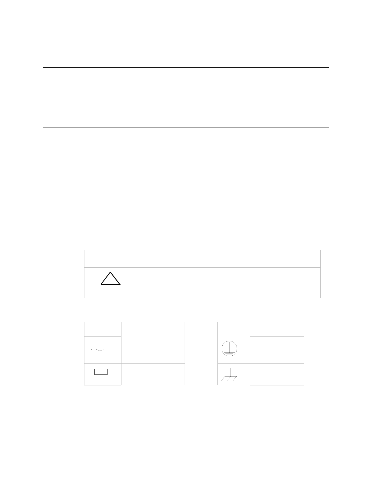
Symbol Definition Symbol Definition
Note:
For additional symbols, refer to “Cautions” listed earlier in this preface.
Applicable testing is routinely performed as a condition of manufacturing on all units to
ensure compliance with safety requirements of EN60950.
Type of power cord required for use in the European Community .
CAUTION: Double-pole/Neutral Fusing.
ACHTUNG: Zweipolige bzw. Neutralleiter-Sicherung.
Alternating Current.
Fuse.
Protective Earth.
Chassis Ground.
Rev. Field v
Page 8

Preface Product Name Field
Warranty Policy
This Comtech EFData product is warranted against defects in material and workmanship
for a period of one year from the date of shipment. During the warranty period, Comtech
EFData will, at its option, repair or replace products that prove to be defective.
For equipment under warranty, the customer is responsible for freight to Comtech
EFData and all related custom, taxes, tariffs, insurance, etc. Comtech EFData is
responsible for the freight charges
the customer. Comtech EFData will return the equipment by the same method (i.e., Air,
Express, Surface) as the equipment was sent to Comtech EFData.
only
for return of the equipment from the factory to
Limitations of Warranty
The foregoing warranty shall not apply to defects resulting from improper installation or
maintenance, abuse, unauthorized modification, or operation outside of environmental
specifications for the product, or, for damages that occur due to improper repackaging of
equipment for return to Comtech EFData.
No other warranty is expressed or implied. Comtech EFData specifically disclaims the
implied warranties of merchantability and fitness for particular purpose.
Exclusive Remedies
The remedies provided herein are the buyer's sole and exclusive remedies. Comtech
EFData shall not be liable for any direct, indirect, special, incidental, or consequential
damages, whether based on contract, tort, or any other legal theory.
Disclaimer
Comtech EFData has reviewed this manual thoroughly in order that it will be an easy-touse guide to your equipment. All statements, technical information, and
recommendations in this manual and in any guides or related documents are believed
reliable, but the accuracy and completeness thereof are not guaranteed or warranted, and
they are not intended to be, nor should they be understood to be, representations or
warranties concerning the products described. Further, Comtech EFData reserves the
right to make changes in the specifications of the products described in this manual at any
time without notice and without obligation to notify any person of such changes.
If you have any questions regarding your equipment or the information in this manual,
please contact the Comtech EFData Customer Support Department.
vi Rev. Field
Page 9
Chapter 1.
INTRODUCTION
1
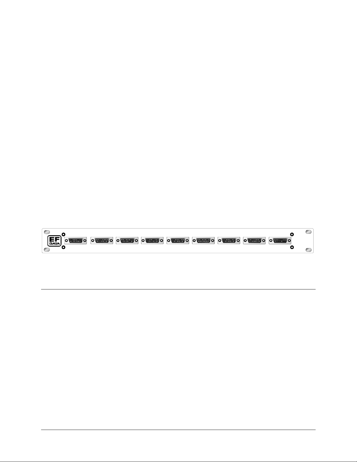
The UB-54 (Figure 1- 1) functions as an 8-channel multiplexer (MUX) or 8-channel
demultiplexer (DEMUX) data breakout panel in one sm all, rack -mountable unit.
TRIB 1 DATA
1.1 Overview
The breakout panel is used to provide a convenient access to tributary data when an
8-channel MUX or 8-channel DEMUX is used.
Major UB-54 features include:
TRIB 2 DAT A TRIB 3 DAT A TRIB 4 DA T A TRIB 5 DA TA TRIB 6 DAT A
J3
Figure 1-1. UB-54 Breakout Panel
Breakout of the 100-pin, 8-channel MUX interface connector through nine
•
standard 15-pin D connectors (8 tributary connectors plus 1 auxiliary circuit
connector). Refer to the SDM-300 Satellite Modem Installation and
Operation manual for more information.
Breakout of the three rear panel 25-pin D 8 channel DEMUX interface
•
connectors through nine standard 15-pin D connectors (8 tributary
connectors plus 1 auxiliary circuit connector). Refer to the SDR-54 Satellite
Demodulator Installation and Operation manual for more information.
J5 J6
TRIB 7 DATA
TRIB 8 DATA AUX
UB-54
BREAKOUT
MUX / DEMUX
J9J8J7J4J1 J2
Rev. 1 1–1
Page 10

Introduction UB-54 Breakout Panel
An auxiliary circuit connector to provide easy access to 8-channel Mux
•
Master Clock inputs, Demod and Mod fault indicators, and Demux aggregate
clock and data signals.
1.2 Description
The UB-54 is a standard one unit (1U) rack-mountable chassis.
The unit consists of a printed circuit board and connectors. The connectors are located at
the front and rear panels. Refer to Chapter 2 for connector specifications.
The UB-54 consists of the following assemblies:
Assembly Part #
Chassis AS/5986
Printed Circuit Board AS/6027
Note:
The electrical specifications for the UB-54 meet or exceed the electrical
requirements of the interfacing modem.
Refer to Figure 1-2 for a schematic illustration of the breakout panel.
1–2 Rev. 1
Page 11

UB-54 Breakout Panel Introduction
This page is intentionally left blank.
Rev. 1 1–3
Page 12

Introduction UB-54 Breakout Panel
MUX
J10
100
MDR100PCR01
TRIB 1 TRIB 2
J1
DSB15FRPCTH
GND
CTS422A1
100
CTS422B1
99
99
98
97
96
95
94
93
92
91
90
89
88
87
86
85
84
83
82
81
80
79
78
77
76
75
74
73
72
71
70
69
68
67
66
65
64
63
62
61
60
59
58
57
56
55
54
53
52
51
50
49
48
47
46
45
44
43
42
41
40
39
38
37
36
35
34
33
32
31
30
29
28
27
26
25
24
23
22
21
20
19
18
17
16
15
14
13
12
11
10
9
8
7
6
5
4
3
2
1
TC422A_1
98
TC422B_1
97
TD422A_1
96
TD422B_1
95
CTS232_1
94
TD232_1
93
TC232_1
92
91
CTS422A2
90
CTS422B2
89
TC422A_2
88
TC422B_2
87
TD422A_2
86
TD422B_2
85
CTS232_2
84
TD232_2
83
TC232_2
82
81
CTS422A3
80
CTS422B3
79
TC422A_3
78
TC422B_3
77
TD422A_3
76
TD422B_3
75
CTS232_3
74
TD232_3
73
TC232_3
72
71
CTS422A4
70
CTS422B4
69
TC422A_4
68
TC422B_4
67
TD422A_4
66
TD422B_4
65
CTS232_4
64
TD232_4
63
TC232_4
62
61
CTS422A5
60
CTS422B5
59
TC422A_5
58
TC422B_5
57
TD422A_5
56
TD422B_5
55
CTS232_5
54
TD232_5
53
TC232_5
52
51
CTS422A6
50
CTS422B6
49
TC422A_6
48
TC422B_6
47
TD422A_6
46
TD422B_6
45
CTS232_6
44
TD232_6
43
TC232_6
42
41
CTS422A7
40
CTS422B7
39
TC422A_7
38
TC422B_7
37
TD422A_7
36
TD422B_7
35
CTS232_7
34
TD232_7
33
TC232_7
32
31
CTS422A8
30
CTS422B8
29
TC422A_8
28
TC422B_8
27
TD422A_8
26
TD422B_8
25
CTS232_8
24
TD232_8
23
TC232_8
22
21
MC-A
20
MC-B
19
18
RR-A
17
RR+B
16
15
RD-A
14
RD+B
13
12
RT-A
11
RT+B
10
9
MF
8
DF
7
6
5
4
3
2
1
815714613512411310291
E1
E2
E3
(CARR IER DET E CT)
E26
E28
J2
DSB15FRPCTH
E25
E27
TRIB 3 TRIB 4
J3
DSB15FRPCTH
815714613512411310291
E4
E5
E6
J4
DSB15FRPCTH
815714613512411310291
E7
E8
E9
815714613512411310291
E10
E11
E12
A
B
C
D
E
F
G
H
I
Figure 1-2. UB-54 Breakout Panel Schematic
1–4 Rev. 1
Page 13

UB-54 Breakout Panel Introduction
TRIB 5
J5
DSB15FRPCTH
TRIB 6 TRIB 7 TRIB 8
J6
DSB15FRPCTH
815714613512411310291
E13
E14
E15
J7
DSB15FRPCTH
815714613512411310291
E16
E17
E18
J8
DSB15FRPCTH
815714613512411310291
E19
E20
E21
815714613512411310291
E22
E23
E24
J9
DSB15FRPCTH
AUX
815714613512411310291
A
B
C
D
E
F
G
H
I
DEMUX
RX AGGR
DEMUX
TRIBS 1-4
DEMUX
TRIBS 5-8
DSB25FRPC02
DSB25FRPC02
DSB25FRPC02
J11
J12
J13
RD422A_1
1
14
RD422B_ 1
2
RC422A_ 1
RC422B_1
15
RD-A
3
16
DMX_SY NC
4
RD+B
17
RT-A
5
DMX_MODE
RT+B
18
RD422A_ 2
6
RD422B_2
19
7
20
DF
RR+B
8
RC422A_2
21
RC422B_2
9
RD422A_ 3
22
RD422B_3
10
RC422A_3
23
11
RC422B_3
24
RD422A_ 4
12
RD422B_4
25
RC422A_4
13
RC422B_4
RD422A_1
1
RD422B_1
14
RC422A_ 1
2
RC422B_ 1
15
3
RD232_1
16
RC232_1
RD422A_ 2
4
RD422B_ 2
17
RC422A_2
5
RC422B_2
18
6
RD232_2
19
RC232_2
RD422A_3
7
RD422B_3
20
8
RC422A_ 3
21
RC422B_ 3
RD232_3
9
RC232_3
22
10
RD422A_ 4
23
RD422B_ 4
11
RC422A_4
24
RC422B_4
RD232_4
12
RC232_4
25
13
RD422A_ 5
1
RD422B_5
14
RC422A_5
2
RC422B_5
15
RD232_5
3
16
RC232_5
RD422A_6
4
17
RD422B_ 6
5
RC422A_ 6
RC422B_6
18
6
RD232_6
19
RC232_6
RD422A_ 7
7
20
RD422B_7
RC422A_7
8
21
RC422B_ 7
RD232_7
9
RC232_7
22
RD422A_8
10
23
RD422B_ 8
11
RC422A_ 8
RC422B_8
24
RD232_8
12
RC232_8
25
13
E33
E35
E34
E36
RD-A
DMX_SY NC
RD+B
RT-A
DMX_MODE
RT+B
DF
RR+B
E29
E31
E30
E32
TD422A_1
TD422B_1
TC422A_1
TC422B_1
TD232_1
TC232_1
TD422A_2
TD422B_2
TC422A_2
TC422B_2
TD232_2
TC232_2
TD422A_3
TD422B_3
TC422A_3
TC422B_3
TD232_3
TC232_3
TD422A_4
TD422B_4
TC422A_4
TC422B_4
TD232_4
TC232_4
TD422A_5
TD422B_5
TC422A_5
TC422B_5
TD232_5
TC232_5
TD422A_6
TD422B_6
TC422A_6
TC422B_6
TD232_6
TC232_6
TD422A_7
TD422B_7
TC422A_7
TC422B_7
TD232_7
TC232_7
TD422A_8
TD422B_8
TC422A_8
TC422B_8
TD232_8
TC232_8
Figure 1-2. UB-54 Breakout Panel Schematic (continued)
Rev. 1 1–5
Page 14

Introduction UB-54 Breakout Panel
This page is intentionally left blank.
1–6 Rev. 1
Page 15

This chapter provides unpacking and installation instructions, and a description of
external connections.
2.1 Unpacking
The breakout panel and manual are packaged in a pre-formed, reusable, cardboard carton
containing foam spacing for maximum protection.
CAUTION
1. Cut the tape at the top of the carton, where it is labeled “OPEN THIS END.”
2. Lift out the cardboard/foam spacer covering the breakout panel.
3. Remove the breakout panel, manual, and power cord from the carton.
4. Save the packing material for reshipment.
5. Inspect the equipment for any possible damage incurred during shipment.
6. Check the equipment against the packing list to ensure the shipment is correct.
7. Refer to Section 2.2 for installation instructions.
Chapter 2.
INSTALLATION
2
Do not use any cutting tool that will extend more than 1”, (2.540 cm), into the
container. This can cause damage to the breakout panel.
Rev. 1 2–1
Page 16

Installation UB-54 Breakout Panel
2.2 Installation
The breakout panel arrives fully assembled from the factory. Install the breakout panel as
follows:
1. Position the breakout panel in the rack.
2. Secure the breakout panel to the rack using 10-32 screws.
3. Connect the cables to the front and/or rear panel (refer to Figure 2-1). Refer to
Section 2.3 for connector pinout, placement, and function.
TRIB 1 DATA
TRIB 2 DATA TRIB 3 DATA TRIB 4 DATA TRIB 5 DATA TRIB 6 DATA
J3
MUX DATA
J10
J5 J6
RX AGGREGATE DEMUX T1-4 DEMUX T5-8
J11
TRIB 7 DATA
J12 J13
TRIB 8 DATA AUX
MUX / DEMUX
J9J8J7J4J1 J2
Figure 2-1. UB-54 Front and Rear Views
Note:
One UB-54 breakout panel can be used with a multiplexer or a demultiplexer,
but not both at the same time.
4. (Used with a Multiplexer only) Connect breakout panel to the SDM-300 Satellite
Modem using a 100-pin ribbon cable conforming to Table 2-12, (Comtech
EFData Part No. CA/90101G100-3 or equivalent) as shown in Figure 2-2.
UB-54
BREAKOUT
2–2 Rev. 1
Page 17

UB-54 Breakout Panel Installation
R
8 CHANNEL DEMULTIPLEXER
8 CHANNEL MULTIPLEXER
APPLICATION
APPLICATIO N
TRIB 1 DATA TRIB 2 D ATA TRIB 3 DATA TRIB 4 DATA TRIB 5 DATA TRIB 6 DATA TRIB 7 DATA TRIB 8 DATA AUX
J2 J3
J4J1
J5 J6
J7
J8
TO J10
100 PIN
SHIELDED RIBBON
CABLE
TO MULTIPLEXER
INTERFACE I/O
TRANSMIT
TRANSMIT
SDM-300
SATELLI TE M ODE M
A
F
L
A
RECEIVE
A
U
R
L
T
M
RECEI VE
COMMO N
STORED
POWER ON
TRANSMITTERON
CARRIE R DETEC T
TESTMODE
ENTER
CLEAR
Figure 2-2. UB-54 to SDM-300 Interconnection Diagram
5. (Used with DEMUX only) Connect the breakout panel to the SDR-54
Demodulator using three standard 25-pin interface cables conforming to Tables
2-13, 2-14, and 2-15 as shown in Figure 2-3.
UB-54
UB-54
BREAKOU T
MUX / DEMUX
J9
SDM-300 W/INTEGRATED
8 CHANNEL MULTIPLEXER
DEMUX
TRIBS 5-8
TRIB 1 DATA TRI B 2 D ATA TRIB 3 DATA TRIB 4 DATA TRI B 5 D ATA TRIB 6 D ATA TRIB 7 DATA TRIB 8 DATA A UX
J7
M & C
REMOTE
SDR-54
J13
J6
POWER
STATUS
J2 J3
CARRIER
FAULT
DETE CT
J4J1
J5 J6
J12
DEMUX
TRIBS 1-4
J5 J4
ANTENNA
ALIGNMENT
TO RX
AGGREGA T E J11
LNB
POWER
J8
SATELLITE DATA
J9
RECEIVER
UB-54
BREAKOUT
UB-54
MUX / DEMUX
SDR-54 W/ INTEGRATED
8 CHANNEL DEM ULTIPLEXE
Figure 2-3. UB-54 to SDR-54 Interconnection Diagram
6. If problems exist with the installation, contact Comtech EFData Customer
Support for additional information.
Rev. 1 2–3
Page 18

Installation UB-54 Breakout Panel
2.3 External Connections and Circuit Assignments
2.3.1 Front Panel Connectors
The location of the connectors are shown in Figure 2-1. Refer to Table 2-1 for a list of
UB-54 front panel connectors.
Table 2-1. Front Panel Connectors
Ref. Desig. Type Interface Function
J1 15-pin D socket EIA-422 or EIA-232 Tributary 1 Clock and Data
J2 15-pin D socket EIA-422 or EIA-232 Tributary 2 Clock and Data
J3 15-pin D socket EIA-422 or EIA-232 Tributary 3 Clock and Data
J4 15-pin D socket EIA-422 or EIA-232 Tributary 4 Clock and Data
J5 15-pin D socket EIA-422 or EIA-232 Tributary 5 Clock and Data
J6 15-pin D socket EIA-422 or EIA-232 Tributary 6 Clock and Data
J7 15-pin D socket EIA-422 or EIA-232 Tributary 7 Clock and Data
J8 15-pin D socket EIA-422 or EIA-232 Tributary 8 Clock and Data
J9 15-pin D socket Auxiliary Data
2–4 Rev. 1
Page 19

UB-54 Breakout Panel Installation
2.3.2 Circuit Assignments for Front Panel Connectors
Refer to Table 2-2 through 2-10 for circuit assignments.
Table 2-2. Tributary #1 Circuit Assignments (J1)
TRIB 1
J1
Pin # Circuit Description Circuit Description
1 CTS422A EIA-422, Clear to Send A(-) - N/A
2,5,11 GND Ground GND Ground
3
4 TD422A EIA-422, Transmit Data A(-) RD422A EIA-422, Receive Data A(-)
6 TD232 EIA-232, Transmit Data RD232 EIA-232, Receive Data
9 CTS422B EIA-422, Clear to Send B(+) - N/A
10
12 TD422B EIA-422, Transmit Data B(+) RD422B EIA-422, Receive Data B(+)
13 CTS232 EIA-232, Clear to Send - N/A
14 TC232 EIA-232, Transmit Clock RC232 EIA-232, Receive Clock
TC422B EIA-422, Transmit Clock B(+) RC422B EIA-422, Receive Clock B(+)
TC422A EIA-422, Transmit Clock A(-)
MUX DEMUX
RC422A EIA-422, Receive Clock A(-)
Table 2-3. Tributary #2 Circuit Assignments (J2)
TRIB 2
J2
Pin # Circuit Description Circuit Description
1 CTS422A EIA-422, Clear to Send A(-) - N/A
2,5,11 GND Ground GND Ground
3
4 TD422A EIA-422, Transmit Data A(-) RD422A EIA-422, Receive Data A(-)
6 TD232 EIA-232, Transmit Data RD232 EIA-232, Receive Data
9 CTS422B EIA-422, Clear to Send B(+) - N/A
10
12 TD422B EIA-422, Transmit Data B(+) RD422B EIA-422, Receive Data B(+)
13 CTS232 EIA-232, Clear to Send - N/A
14 TC232 EIA-232, Transmit Clock RC232 EIA-232, Receive Clock
TC422B EIA-422, Transmit Clock B(+) RC422B EIA-422, Receive Clock B(+)
TC422A EIA-422, Transmit Clock A(-)
MUX DEMUX
RC422A EIA-422, Receive Clock A(-)
Rev. 1 2–5
Page 20

Installation UB-54 Breakout Panel
Table 2-4. Tributary #3 Circuit Assignments (J3)
TRIB 3
J3
Pin # Circuit Description Circuit Description
1 CTS422A EIA-422, Clear to Send A(-) - N/A
2,5,11 GND Ground GND Ground
3
4 TD422A EIA-422, Transmit Data A(-) RD422A EIA-422, Receive Data A(-)
6 TD232 EIA-232, Transmit Data RD232 EIA-232, Receive Data
9 CTS422B EIA-422, Clear to Send B(+) - N/A
10
12 TD422B EIA-422, Transmit Data B(+) RD422B EIA-422, Receive Data B(+)
13 CTS232 EIA-232, Clear to Send - N/A
14 TC232 EIA-232, Transmit Clock RC232 EIA-232, Receive Clock
TC422B EIA-422, Transmit Clock B(+) RC422B EIA-422, Receive Clock B(+)
TC422A EIA-422, Transmit Clock A(-)
MUX DEMUX
RC422A EIA-422, Receive Clock A(-)
Table 2-5. Tributary #4 Circuit Assignments (J4)
TRIB 4
J4
Pin # Circuit Description Circuit Description
1 CTS422A EIA-422, Clear to Send A(-) - N/A
2,5,11 GND Ground GND Ground
3
4 TD422A EIA-422, Transmit Data A(-) RD422A EIA-422, Receive Data A(-)
6 TD232 EIA-232, Transmit Data RD232 EIA-232, Receive Data
9 CTS422B EIA-422, Clear to Send B(+) - N/A
10
12 TD422B EIA-422, Transmit Data B(+) RD422B EIA-422, Receive Data B(+)
13 CTS232 EIA-232, Clear to Send - N/A
14 TC232 EIA-232, Transmit Clock RC232 EIA-232, Receive Clock
TC422B EIA-422, Transmit Clock B(+) RC422B EIA-422, Receive Clock B(+)
TC422A EIA-422, Transmit Clock A(-)
MUX DEMUX
RC422A EIA-422, Receive Clock A(-)
Table 2-6. Tributary #5 Circuit Assignments (J5)
TRIB 5
J5
Pin# Circuit Description Circuit Description
1 CTS422A EIA-422, Clear to Send A(-) - N/A
2,5,11 GND Ground GND Ground
3
4 TD422A EIA-422, Transmit Data A(-) RD422A EIA-422, Receive Data A(-)
6 TD232 EIA-232, Transmit Data RD232 EIA-232, Receive Data
9 CTS422B EIA-422, Clear to Send B(+) - N/A
10
12 TD422B EIA-422, Transmit Data B(+) RD422B EIA-422, Receive Data B(+)
13 CTS232 EIA-232, Clear to Send - N/A
14 TC232 EIA-232, Transmit Clock RC232 EIA-232, Receive Clock
2–6 Rev. 1
TC422B EIA-422, Transmit Clock B(+) RC422B EIA-422, Receive Clock B(+)
TC422A EIA-422, Transmit Clock A(-)
MUX DEMUX
RC422A EIA-422, Receive Clock A(-)
Page 21

UB-54 Breakout Panel Installation
Table 2-7. Tributary #6 Circuit Assignments (J6)
TRIB 6
J6
Pin # Circuit Description Circuit Description
1 CTS422A EIA-422, Clear to Send A(-) - N/A
2,5,11 GND Ground GND Ground
3
4 TD422A EIA-422, Transmit Data A(-) RD422A EIA-422, Receive Data A(-)
6 TD232 EIA-232, Transmit Data RD232 EIA-232, Receive Data
9 CTS422B EIA-422, Clear to Send B(+) - N/A
10
12 TD422B EIA-422, Transmit Data B(+) RD422B EIA-422, Receive Data B(+)
13 CTS232 EIA-232, Clear to Send - N/A
14 TC232 EIA-232, Transmit Clock RC232 EIA-232, Receive Clock
TC422B EIA-422, Transmit Clock B(+) RC422B EIA-422, Receive Clock B(+)
TC422A EIA-422, Transmit Clock A(-)
MUX DEMUX
RC422A EIA-422, Receive Clock A(-)
Table 2-8. Tributary #7 Circuit Assignments (J7)
TRIB 7
J7
Pin # Circuit Description Circuit Description
1 CTS422A EIA-422, Clear to Send A(-) - N/A
2,5,11 GND Ground GND Ground
3
4 TD422A EIA-422, Transmit Data A(-) RD422A EIA-422, Receive Data A(-)
6 TD232 EIA-232, Transmit Data RD232 EIA-232, Receive Data
9 CTS422B EIA-422, Clear to Send B(+) - N/A
10
12 TD422B EIA-422, Transmit Data B(+) RD422B EIA-422, Receive Data B(+)
13 CTS232 EIA-232, Clear to Send - N/A
14 TC232 EIA-232, Transmit Clock RC232 EIA-232, Receive Clock
TC422B EIA-422, Transmit Clock B(+) RC422B EIA-422, Receive Clock B(+)
TC422A EIA-422, Transmit Clock A(-)
MUX DEMUX
RC422A EIA-422, Receive Clock A(-)
Table 2-9. Tributary #8 Circuit Assignments (J8)
TRIB 8
J8
Pin # Circuit Description Circuit Description
1 CTS422A EIA-422, Clear to Send A(-) - N/A
2,5,11 GND Ground GND Ground
3
4 TD422A EIA-422, Transmit Data A(-) RD422A EIA-422, Receive Data A(-)
6 TD232 EIA-232, Transmit Data RD232 EIA-232, Receive Data
9 CTS422B EIA-422, Clear to Send B(+) - N/A
10
12 TD422B EIA-422, Transmit Data B(+) RD422B EIA-422, Receive Data B(+)
13 CTS232 EIA-232, Clear to Send - N/A
14 TC232 EIA-232, Transmit Clock RC232 EIA-232, Receive Clock
Rev. 1 2–7
TC422B EIA-422, Transmit Clock B(+) RC422B EIA-422, Receive Clock B(+)
TC422A EIA-422, Transmit Clock A(-)
MUX DEMUX
RC422A EIA-422, Receive Clock A(-)
Page 22

Installation UB-54 Breakout Panel
Table 2-10. Auxiliary Circuit Pin Assignments (J9)
AUX
J9
Pin # Circuit Description Circuit Description
1 MC-A Master Clock A(-) - N/A
2,5,11 GND Ground GND Ground
3
4 RD-A EIA-422, Receive Data A(-) RD-A EIA-422, Receiver Data A(-)
6 RR+B Receiver Ready B(+) RR Receiver Ready
7 - N/A DSYNC DEMUX SYNC
8 MF MOD Fault - N/A
9 MC-B Master Clock B(+) - N/A
10
12 RD+B EIA-422, Receive Data B(+) RD+B EIA-422, Receiver Data B(+)
13 RR-A Receiver Ready A(-) - N/A
14 - N/A DMODE DEMUX Mode
15 DF DEMOD Fault --- N/A
RT+B EIA-422, Receive Timing B(+) RT+B EIA-422, Receiver Timing B(+)
RT-A
EIA-422, Receive Timing A(-)
MUX DEMUX
RT-A
EIA-422, Receiver Timing A(-)
2–8 Rev. 1
Page 23

UB-54 Breakout Panel Installation
2.3.3 Rear Panel Connectors
The location of the connectors are shown in Figure 2-1. Refer to Table 2-11 for a list of
UB-54 rear panel connectors.
Table 2-11. Rear Panel Connectors
Ref. Desig. Type Interface Function
J10 100-pin miniature D MUX Data and Tributaries 1-8
J11 25-pin D socket Rx Aggregate
J12 25-pin D socket DEMUX Tributaries 1-4
J13 25-pin D socket DEMUX Tributaries 5-8
2.3.4 Circuit Assignments for Rear Panel Connectors
Refer to Tables 2-12, 2-13, 2-14, and 2-15 for circuit assignments for rear panel
connectors.
Rev. 1 2–9
Page 24

Installation UB-54 Breakout Panel
Table 2-12. MUX Data Pin Assignments (J10)
J10 MUX Data
Pin # Circuit Description Pin # Circuit Description
1 - N/A 51 GND Ground
2 - N/A 52 TC232_5 EIA-232,Transmit Clock,TRIB5
3 - N/A 53 TD232_5 EIA-232,Transmit Data,TRIB5
4 - N/A 54 CTS232_5 EIA-232,Clear to Send,TRIB5
5 GND Ground 55 TD422B_5 EIA-422,Transmit Data B(+),TRIB5
6 GND Ground 56 TD422A_5 EIA-422,Transmit Data A(-),TRIB5
7 DF DEMOD Fault 57 TC422B_5 EIA-422,Transmit Clock B(+),TRIB5
8 MF MOD Fault 58 TC422A_5 EIA-422,Transsmit Clock A(-),TRIB5
9 GND Ground 59 CTS422B5 EIA-422,Clear to Send B(+),TRIB5
10 RT+B Receive Timing B(+) 60 CTS422A5 EIA-422,Clear to Send A(-),TRIB5
11 RT-A Receive Timing A(-) 61 GND Ground
12 GND Ground 62 TC232_4 EIA-232,Transmit Clock,TRIB4
13 RD+B Receive Data B(+) 63 TD232_4 EIA-232,Transmit Data,TRIB4
14 RD-A Receive Data A(-) 64 CTS232_4 EIA-232,Clear to Send,TRIB4
15 GND Ground 65 TD422B_4 EIA-422,Transmit Data B(+),TRIB4
16 RR+B Receiver Ready B(+) 66 TD422A_4 EIA-422,Transmit Data A(-),TRIB4
17 RR-A Receiver Ready A(-) 67 TC422B_4 EIA-422,Transmit Clock B(+),TRIB4
18 GND Ground 68 TC422A_4 EIA-422,Transmit Clock A(-),TRIB4
19 TMUXDAT Transmit Aggregate Data 69 CTS422B4 EIA-422,Clear to Send B(+),TRIB4
20 TMUXCLK Transmit Aggregate Clock 70 CTS422A4 EIA-422,Clear to Send A(-),TRIB4
21 GND Ground 71 GND Ground
22 TC232_8 EIA-232,Transmit Clock,TRIB8 72 TC232_3 EIA-232,Transmit Clock,TRIB3
23 TD232_8 EIA-232,Transmit Data,TRIB8 73 TD232_3 EIA-232,Transmit Data,TRIB3
24 CTS232_8 EIA-232,Clear to Send,TRIB8 74 CTS232_3 EIA-232,Clear to Send,TRIB3
25 TD422B_8 EIA-422,Transmit Data B(+),TRIB8 75 TD422B_3 EIA-422,Transmit Data B(+),TRIB3
26 TD422A_8 EIA-422,Transmit Data (-),TRIB8 76 TD422A_3 EIA-422,Transmit Data A(-),TRIB3
27 TC422B_8 EIA-422,Transmit Clock B(+),TRIB8 77 TC422B_3 EIA-422,Transmit Clock B(+),TRIB3
28 TC422A_8 EIA-422,Transmit Clock A(-),TRIB8 78 TC422A_3 EIA-422,Transmit Clock A(-),TRIB3
29 CTS422B8 EIA-422,Clear to Send B(+),TRIB8 79 CTS422B3 EIA-422,Clear to Send B(+),TRIB3
30 CTS422A8 EIA-422,Clear to Send A(-),TRIB8 80 CTS422A3 EIA-422,Clear to Send A(-),TRIB3
31 GND Ground 81 GND Ground
32 TC232_7 EIA-232,Transmit Clock,TRIB7 82 TC232_2 EIA-232,Transmit Clock,TRIB2
33 TD232_7 EIA-232,Transmit Data,TRIB7 83 TD232_2 EIA-232,Transmit Data,TRIB2
34 CTS232_7 EIA-232,Clear to Send,TRIB7 84 CTS232_2 EIA-232,Clear to Send,TRIB2
35 TD422B_7 EIA-422,Transmit Data B(+),TRIB7 85 TD422B_2 EIA-422,Transmit Data B(+),TRIB2
36 TD422A_7 EIA-422,Transmit Data A(-),TRIB7 86 TD422A_2 EIA-422,Transmit Data A(-),TRIB2
37 TC422B_7 EIA-422,Transmit Clock B(+),TRIB7 87 TC422B_2 EIA-422,Transmit Clock B(+),TRIB2
38 TC422A_7 EIA-422,Transmit Clock A(-),TRIB7 88 TC422A_2 EIA-422,Transmit Clock A(-),TRIB2
39 CTS422B7 EIA-422,Clear to Send B(+),TRIB7 89 CTS422B2 EIA-422,Clear to Send B(+),TRIB2
40 CTS422A7 EIA-422,Clear to Send A(-),TRIB7 90 CTS422A2 EIA-422,Clear to Send A(-),TRIB2
41 GND Ground 91 GND Ground
42 TC232_6 EIA-232,Transmit Clock,TRIB6 92 TC232_1 EIA-232,Transmit Clock,TRIB1
43 TD232_6 EIA-232,Transmit Data,TRIB6 93 TD232_1 EIA-232,Transmit Data,TRIB1
44 CTS232_6 EIA-232,Clear to Send,TRIB6 94 CTS232_1 EIA-232,Clear to Send,TRIB1
45 TD422B_6 EIA-422,Transmit Data B(+),TRIB6 95 TD422B_1 EIA-422,Transmit Data B(+),TRIB1
46 TD422A_6 EIA-422,Transmit Data A(-),TRIB6 96 TD422A_1 EIA-422,Transmit Data A(-),TRIB1
47 TC422B_6 EIA-422,Transmit Clock B(+),TRIB6 97 TC422B_1 EIA-422,Transmit Clock B(+),TRIB1
48 TC422A_6 EIA-422,Transmit Clock A(-),TRIB6 98 TC422A_1 EIA-422,Transmit Clock A(-),TRIB1
49 CTS422B6 EIA-422,Clear to Send B(+),TRIB6 99 CTS422B1 EIA-422,Clear to Send B(+),TRIB1
50 CTS422A6 EIA-422,Clear to Send A(-),TRIB6 100 CTS422A1 EIA-422,Clear to Send A(-),TRIB1
2–10 Rev. 1
Page 25

UB-54 Breakout Panel Installation
Table 2-13. Receive Aggregate Pin Assignments (J11)
J11 RX Aggregate
Pin # Circuit Description
1 RD422A_1 EIA-422,Receive Data A(-),TRIB1
2 RC422A_1 EIA-422,Receive Clock A(-),TRIB1
3 RD-A EIA-422, Receive Data A(-)
4 RD+B EIA-422, Receive Data B(+)
5 DMODE DEMUX Mode
6 RD422A_2 EIA-422,Receive Data A(-),TRIB2
7 GND Ground
8 RR+B Receiver Ready B(+)
9 RC422B_2 EIA-422,Receive Clock B(+),TRIB2
10 RD422B_3 EIA-422,Receive Data B(+),TRIB3
11 RC422B_3 EIA-422,Receive Clock B(+),TRIB3
12 RD422B_4 EIA-422,Receive Data B(+),TRIB4
13 RC422B_4 EIA-422,Receive Clock B(+),TRIB4
14 RD422B_1 EIA-422,Receive Data B(+),TRIB1
15 RC422B_1 EIA-422,Receive Clock B(+),TRIB1
16 DSYNC DEMUX SYNC
17 RT-A EIA-422, Receive Timing A(-)
18 RT+B EIA-422, Receive Timing B(+)
19 RD422B_2 EIA-422,Receive Data B(+),TRIB2
20 DF DEMOD Fault (From MUX)
21 RC422A_2 EIA-422,Receive Clock A(-),TRIB2
22 RD422A_3 EIA-422,Receive Data A(-),TRIB3
23 RC422A_3 EIA-422,Receive Clock A(-),TRIB3
24 RD422A_4 EIA-422,Receive Data A(-),TRIB4
25 RC422A_4 EIA-422,Receive Clock A(-),TRIB4
Rev. 1 2–11
Page 26

Installation UB-54 Breakout Panel
Table 2-14. DEMUX T1 Through T4 Pin Assignments (J12)
J12 DEMUX T1 through T4
Pin # Circuit Description
1 RD422A_1 EIA-422,Receive Data A(-),TRIB1
2 RC422A_1 EIA-422,Receive Clock A(-),TRIB1
3 RD232_1 EIA-232,Receive Data A ,TRIB1
4 RD422A_2 EIA-422,Receive Data A(-),TRIB2
5 RC422A_2 EIA-422,Receive Clock A(-),TRIB2
6 RD232_2 EIA-232,Receive Data A ,TRIB2
7 RD422A_3 EIA-422,Receive Data A(-),TRIB3
8 RC422A_3 EIA-422,Receive Clock A(-),TRIB3
9 RD232_3 EIA-232,Receive Data A ,TRIB3
10 RD422A_4 EIA-422,Receive Data A(-),TRIB4
11 RC422A_4 EIA-422,Receive Clock A(-),TRIB4
12 RD232_4 EIA-232,Receive Data A ,TRIB4
13 GND Ground
14 RD422B_1 EIA-422,Receive Data B(+),TRIB1
15 RC422B_1 EIA-422,Receive Clock B(+),TRIB1
16 RC232_1 EIA-232,Receive Clock,TRIB1
17 RD422B_2 EIA-422,Receive Data B(+),TRIB2
18 RC422B_2 EIA-422,Receive Clock B(+),TRIB2
19 RC232_2 EIA-232,Receive Clock,TRIB2
20 RD422B_3 EIA-422,Receive Data B(+),TRIB3
21 RC422B_3 EIA-422,Receive Clock B(+),TRIB3
22 RC232_3 EIA-232,Receive Clock,TRIB3
23 RD422B_4 EIA-422,Recive Data B(+),TRIB4
24 RC422B_4 EIA-422,Receive Clock B(+),TRIB4
25 RC232_4 EIA-232,Receive Clock,TRIB4
2–12 Rev. 1
Page 27

UB-54 Breakout Panel Installation
Table 2-15. DEMUX T5 Through T8 Pin Assignments (J13)
J13 DEMUX T5 through T8
PIN # Circuit Description
1 RD422A_5 EIA-422,Receive Data A(-),TRIB5
2 RC422A_5 EIA-422,Receive Clock A(-),TRIB5
3 RD232_5 EIA-232,Receive Data A ,TRIB5
4 RD422A_6 EIA-422,Receive Data A(-),TRIB6
5 RC422A_6 EIA-422,Receive Clock A(-),TRIB6
6 RD232_6 EIA-232,Receive Data A ,TRIB6
7 RD422A_7 EIA-422,Receive Data A(-),TRIB7
8 RC422A_7 EIA-422,Receive Clock A(-),TRIB7
9 RD232_7 EIA-232,Receive Data A ,TRIB7
10 RD422A_8 EIA-422,Receive Data A(-),TRIB8
11 RC422A_8 EIA-422,Receive Clock A(-),TRIB8
12 RD232_8 EIA-232,Receive Data A ,TRIB8
13 GND GROUND
14 RD422B_5 EIA-422,Receive Data B(+),TRIB5
15 RC422B_5 EIA-422,Receive Clock B(+),TRIB5
16 RC232_5 EIA-232,Receive Clock TRIB5
17 RD422B_6 EIA-422,Receive Data B(+),TRIB6
18 RC422B_6 EIA-422,Receive Clock B(+),TRIB6
19 RC232_6 EIA-232,Receive Clock,TRIB6
20 RD422B_7 EIA-422,Receive Data B(+),TRIB7
21 RC422B_7 EIA-422,Receive Clock B(+),TRIB7
22 RC232_7 EIA-232,Receive Clock,TRIB7
23 RD422B_8 EIA-422,Receive Data B(+),TRIB8
24 RC422B_8 EIA-422,Receive Clock B(+),TRIB8
25 RC232_8 EIA-232,Receive Clock,TRIB8
Rev. 1 2–13
Page 28

Installation UB-54 Breakout Panel
This page is intentionally left blank.
2–14 Rev. 1
Page 29

METRIC CONVERSIONS
Units of Length
Unit
1 centimeter — 0.3937 0.03281 0.01094
Centimeter
Inch
Foot
Yard
Mile
6.214 x 10
Meter
-6
0.01 — —
Kilometer Millimeter
—
-5
0.254 — 25.4
-4
0.3048 — —
-4
0.9144 — —
-4
— — —
1.609 x 10³
1.609 —
1 inch 2.540 — 0.08333 0.2778
1 foot 30.480 12.0 — 0.3333
1 yard 91.44 36.0 3.0 —
1 meter 100.0 39.37 3.281 1.094
1 mile
1 mm — 0.03937 — — — — — —
1 kilometer — — — — 0.621 — — —
1.609 x 10
5
6.336 x 10⁴ 5.280 x 10³ 1.760 x 10³
1.578 x 10
1.893 x 10
5.679 x 10
6.214 x 10
Temperature Conversions
Ounce
Troy
Formulas
C = (F - 32) * 0.555
F = (C * 1.8) + 32
Pound
Avoir.
Pound
Troy
Kilogram
Unit
32° Fahrenheit
212° Fahrenheit
-459.6° Fahrenheit
°°°° Fahrenheit
—
—
—
°°°° Centigrade
0
(water freezes)
100
(water boils)
273.1
(absolute 0)
Units of Weight
Unit
1 gram — 0.03527 0.03215 0.002205 0.002679 0.001
Gram
Ounce
Avoirdupois
1 oz. avoir. 28.35 — 0.9115 0.0625 0.07595 0.02835
1 oz. troy 31.10 1.097 — 0.06857 0.08333 0.03110
1 lb. avoir. 453.6 16.0 14.58 — 1.215 0.4536
1 lb. Troy 373.2 13.17 12.0 0.8229 — 0.3732
1 kilogram
1.0 x 10
3
35.27 32.15 2.205 2.679 —
Page 30

2114
WEST 7TH STREET TEMPE ARIZONA
480 • 333 • 2200
480 • 333
85281
PHONE
• 2161
USA
FAX
 Loading...