

Page 1
COMTECH TECHNOLOGY CO., LTD.
1. GENERAL SPECIFICATION
FM1200RTIM
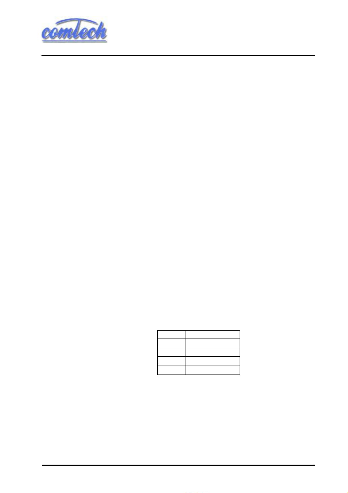
1-1 Input Frequency Range
1-3 One Input Connector
1-4 Nominal Input Impedance
1-5 Tuning Circuit
1-6 IF Frequency
1-7 IF Bandwidth
1-8 Demodulation
1-9 Video Output Polarity
1-10 Operating Voltage
1-1 1 Operating T emperature
1-12 Operating Humidity
1-13 Storage T emperature
1-14 Storage Humidity
1 100 MHz - 1300 MHz
F Fe-Male
75 Ohm
Built-in PLL
479.50 MHz Center
27 MHz Nominal (Selectable)
Phase Locked Loop
Positive Going
+12V (+/-5%)
+5V (+/-5%)
-10oC ~ +60oC
less than 80% R. H. (at 40oC)
-20oC ~ +70oC
less than 95% R. H. (at 40oC)
2. STANDARD TEST CONDITION test for electrical specification shall be
preformed at following condition unless
otherwise specified.
2-1 Ambient Condition
Temperature 25oC +/- 2oC
Humidity 65% +/- 5% R. H.
if no doubt on test results
Temperature +5oC ~ +30oC
Humidity 45% ~ 80% R. H.
could be applied
Note:
SP5055
(PLESSEY)
Note:
T A8804F
2-2 Measurement to Start
2-3 Power Supply
Aug,15, 2001
30 minutes after DC power supplied
Terminal Supply Voltage
+5V +5V (+/-) 0.1V
TU +12V (+/-) 0.1V
SDA specified tuning
SCL pulse
1
Page 2
COMTECH TECHNOLOGY CO., LTD.
FM1200RTIM
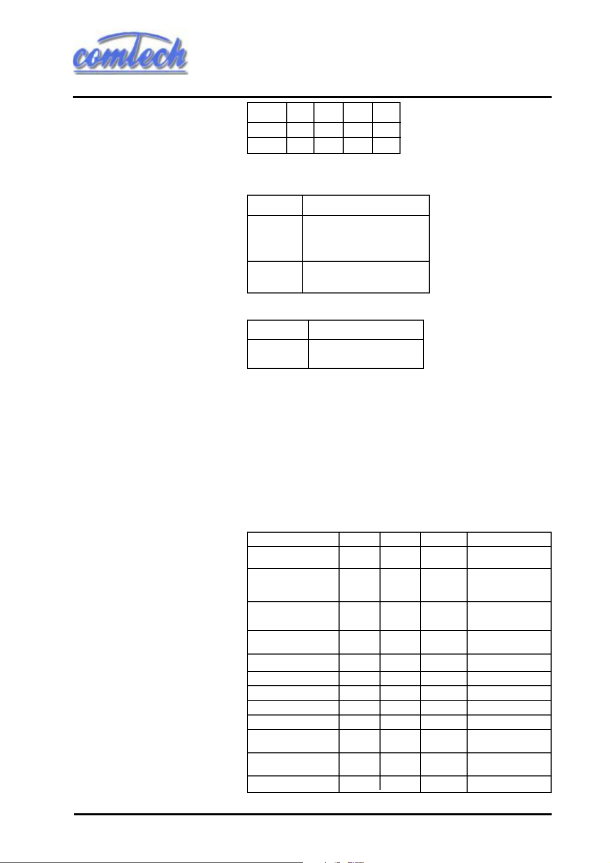
3. CURRENT CONSUMPTION
Terminal Min. Typ. Max. Unit
+5V 190 240 290 mA
TU 0.5 1.0 3.0 mA
4. ABSOLUTE MAXIMUM VOLTAGE
Terminal Max. Supply Voltage
LNB Power DC +25V
+5V DC +5.25V
TU DC +15V
SDA,SCL OV TO The Same V oltage
AS +5V Terminal
Terminal Max. Take Off Current
LNB Power 500mA
B. B. Output 0.5 mA
5. ELECTRICAL SPECIFICATION
under standard test condition
Test Channel: DBS 20 CH
Input Level: -45 dBm
unless otherwise specified
Condition
5-1 Input VSWR
5-2 Noise Figure
5-3 Local Leakage at
Input Terminal
5-4 Tuning V oltage Curve
5-5 Local Oscillator +B Shift
5-6 Local Oscillator
Temperature Drift
5-7 IF 3dB Bandwidth
1 100 ~ 1300 MHz
1 100 ~ 1300 MHz
1579.5~1779.5 MHz
1 100 ~ 1300 MHz
tuning voltage shift
with +B +/- 5%
tuning voltage shift
with -10oC ~ +60oC
3dB down
Min.
2.5V
T yp.
2.0
8.0 dB
-70.0
27
Max.
3.0
12.dB
-63.0
7.0V
+/- 0.8
+/- 1.3
Note
AGC fullgain
dBm
with tuing
PLL locked
MHz
5-8 AFT Output
(2 bit Output)
Aug,15, 2001
Center Frequency
Error (f0)
-2
+2
MHz
2
Page 3
COMTECH TECHNOLOGY CO., LTD.
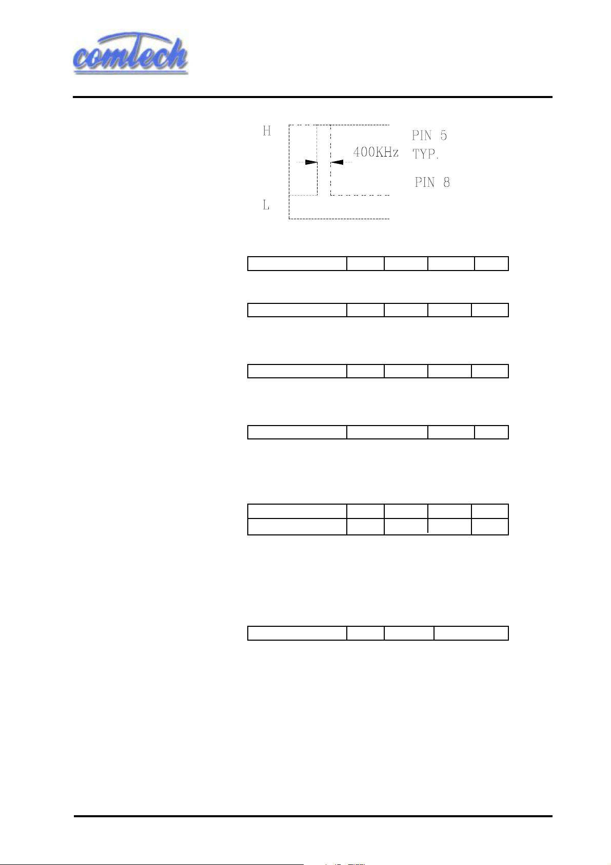
5-9 B. B. Output Characteristics
Condition Min. Typ. Max. Note
FM1200RTIM
1) Video Output Level
2) Gain-Frequency
Response
3) Group Delay Response
4) DG/DP
5) S/N
video waveform white 100% P AL frequency deviation 16 MHz p-p without pre-emphasis
white to SYNC 0.72 0.90 1.12 Vp-p
test modulation frequency: 60 Hz ~ 8 MHz without energy disposal
modulation, reference frequency 100 KHz, IF BW: 27 MHz
Freuqency Response +/- 1 +/- 3 dB
test frequency: 60 Hz ~ 8 MHz without energy disposal modulation,
reference frequency 100 KHz, IF BW: 27 MHz
Group Delay +/- 10 +/- 50 nsec
10 step siaircase 16MHz p-p P AL without energy disposal modulation,
positive video amplifier with de-emphasis should be applied
IF BW: 27 MHz
DG (APL 50%) 4.0 8.0 %
DP (APL 50%) 3.0 5.0 deg
input C/N = 14 dB (Noise BW: 27 MHz)
white 100% video 16 MHz p-p PAL with audio subcarrier modulation
3.4 MHz p-p DEV. @6.5 MHz
positive video amplifier with de-emphasis should be applied 100 Hz ~ 5
MHz unweighted S/N, for power on reset indicator
S/N 34.0 36.0 dB
Aug,15, 2001
3
Page 4
COMTECH TECHNOLOGY CO., LTD.
FM1200RTIM
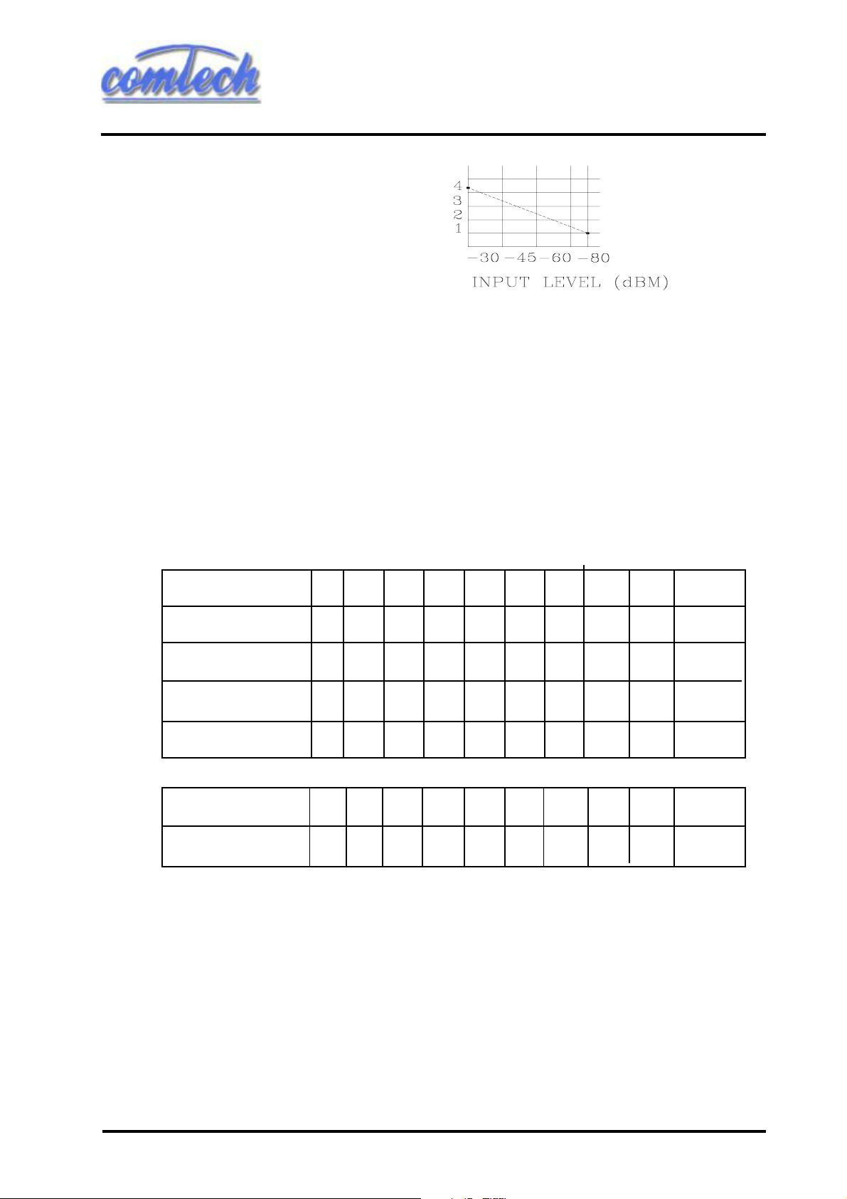
7-1 Signal Level Out Voltage
7-2 IIC Bus
1) SDA, SCL Input Voltage
2) Address
3) SDA, SCL
Input Impedance
4) Date Format
(V)
SIGNAL
LEVEL
OUT
under standard test condition
Condition Min. Typ. Max. Note
High Voltage 3 5 V
Low Voltage 0 1.5 V
C2 (on write data format)
SDA/SCL are in the high impedance and there should be no reliablity
problem with 5V continually on the SDA/SCL if power supply is switched
off.
MSB LSB
Address 1 1 0 0 0 MA1 MA0 0 A BYTE 1
Programmable Divider 0 2
Programmable Divider 27 26 25 24 23 22 21 20 A BYTE 3
Charge Pump and 1 CP T1 T0 1 1 1 OS A BYTE 4
Test Bits
I/O Port Control Bits P7 P6 P5 P4 P3 P2 P1 P0 A BYTE 5
table 1 write data format (MSB is transmitted first)
Address 1 1 0 0 0 MA1 MA0 1 A BYTE1
Status Byte FOR FL I2 I1 I0 A2 A1 A0 A BYTE 2
table 2 read data format
A: acknowledge bit
MA1, MA0: voltage address bits
CP: charge pomp current select
T1: test mode selection
T0: charge pump disable
OS: varactor drive output disable switch
P7, P6, P5, P4, P3, P2, P1, P0: control output states
POR: power on reset indicator
I2, I1, I0: digital information from ports P7, P5 and P4
A2, A1, A0: 5 level ADC data from P6
14 213
212 211 210 29 28 A BYTE 2
Aug,15, 2001
4
Page 5
COMTECH TECHNOLOGY CO., LTD.
FM1200RTIM
Aug,15, 2001
5
 Loading...