

Page 1
p
SEMICONDUCTORS
TIC246B, TIC246C, TIC246D, TIC246E, TIC246M, TIC246N,
TIC246S
• High current triacs
• 16 A RMS
• 70 A Peak
• Glass Passivated Wafer
• 200 V to 800 V Off-State Voltage
• Max I
• 125 A peak current
• Com
DESCRIPTION
This device is a bidirectional triode thyristor (triac) which may be triggered from the off-state
to the on-state by either polarity of gate signal with main Terminal 2 at either polarity.
ABSOLUTE MAXIMUM RATINGS
SILICON BIDIRECTIONAL TRIODE THYRISTOR
of 50 mA (Quadrants 1-3)
GT
liance to ROHS
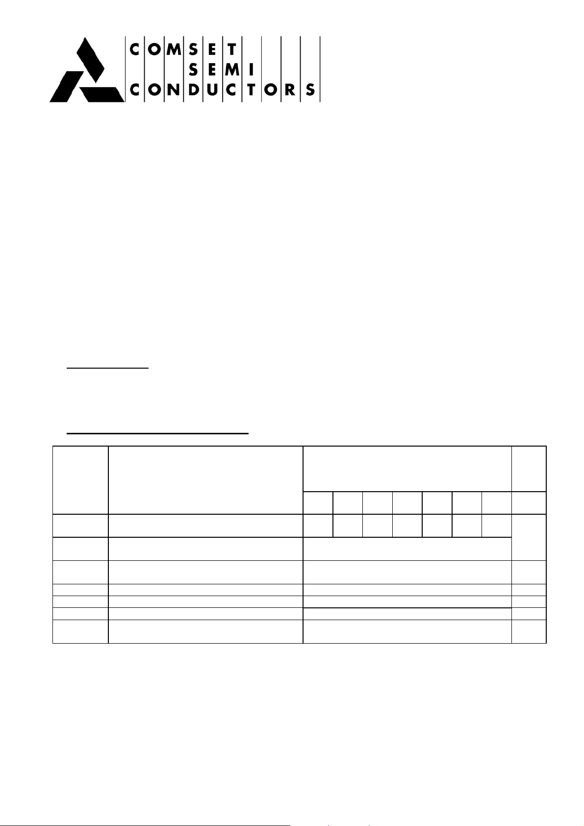
Symbol Ratings
V
DRM
I
T(RMS)
I
TSM
IGM
TC
T
stg
TL
Notes:
Repetitive peak off-state voltage
(see Note1)
Full-cycle RMS on-state current at (or
below) 70°C case temperature (see note2)
Peak on-state surge current full-sine-wave
(see Note3)
Peak gate current ± 1 A
Operating case temperature range -40 to +110 °C
Storage temperature range -40 to +125 °C
Lead temperature 1.6 mm from case for 10
seconds
1. These values apply bidirectionally for any value of resistance between the gate and Main Terminal
1.
2. This value applies for 50-Hz full-sine-wave operation with resistive load. Above 70°C derate
linearly to 110°C case temperature at the rate of 400 mA/°C.
3. This value applies for one 50-Hz full-sine-wave when the device is operating at (or below) the rated
value of peak reverse voltage and on-state current. Surge may be repeated after the device has
returned to original thermal equilibrium.
Value Unit
B C D E M S N
200 300 400 500 600 700 800 V
16 A
125 A
230 °C
Page 1 of 3
Page 2
SEMICONDUCTORS
TIC246B, TIC246C, TIC246D, TIC246E, TIC246M, TIC246N,
TIC246S
THERMAL CHARACTERISTICS
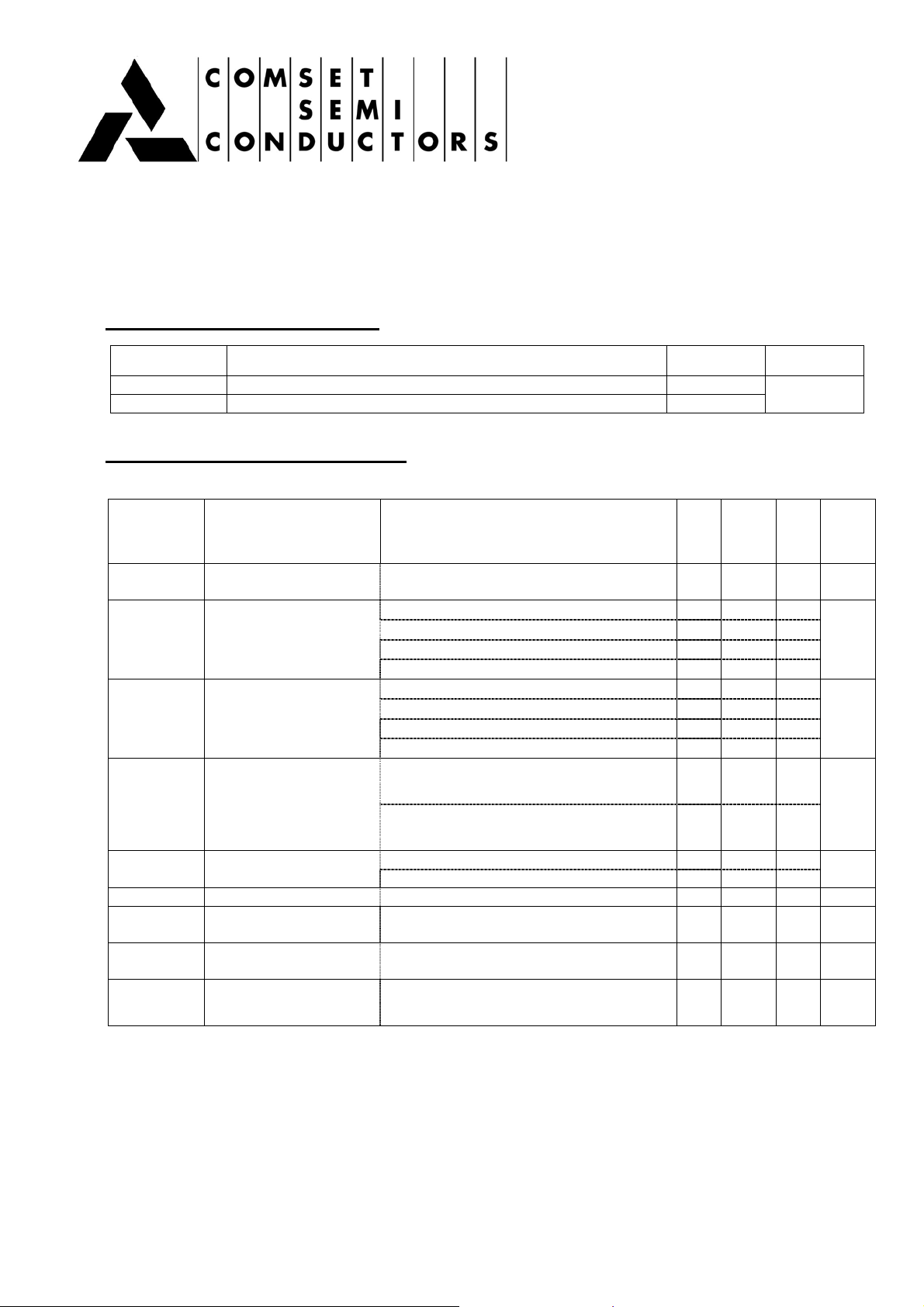
Symbol Ratings Value Unit
R
∂JC
R
∂JA
ELECTRICAL CHARACTERISTICS
TC=25°C unless otherwise noted
Junction to case thermal resistance ≤ 1.9
Junction to free air thermal resistance ≤ 62.5
°C/W
Symbol Ratings
I
DRM
IGT
VGT
IH
IL
VTM
dv/dt
di/dt
dv/dt©
Repetitive peak offstate current
Gate trigger current
Gate trigger voltage
Holding current
Latching current
Peak on-state voltage I
Critical rate of rise of
off-state voltage
Critical rate of rise of
off-state current
Critical rise of
communication voltage
= Rated V
V
D
T
= 110°C
C
V
supply
V
supply
V
supply
V
supply
V
supply
V
supply
V
supply
V
supply
V
supply
initiating I
V
supply
initiating I
V
supply
V
supply
= ± 22.5 A, IG = 50 mA (see Note4) - ±1.4 ±1.7 V
TM
= Rated V
V
DRM
T
= 110°C
C
= Rated V
V
DRM
/dt = 50mA/µs, TC = 110°C
di
G
= Rated V
V
DRM
di/dt = 0.5 I
Test Condition(s)
, , IG = 0,
DRM
= +12 V†, RL = 10 Ω, t
= +12 V†, RL = 10 Ω, t
= -12 V†, RL = 10 Ω, t
= -12 V†, RL = 10 Ω, t
= +12 V†, RL = 10 Ω, t
= +12 V†, RL = 10 Ω, t
= -12 V†, RL = 10 Ω, t
= -12 V†, RL = 10 Ω, t
= +12 V†, IG = 0,
= 100 mA
TM
= -12 V†, IG = 0,
= -100 mA
TM
= > 20 µs
p(g)
= > 20 µs
p(g)
= > 20 µs
p(g)
= > 20 µs
p(g)
= > 20 µs
p(g)
= > 20 µs
p(g)
= > 20 µs
p(g)
= > 20 µs
p(g)
Min Typ Mx Unit
- - ±2 mA
- 12 50
- -19 -50
- -16 -50
- 34 -
- 0.8 2
- -0.8 -2
- -0.8 -2
- 0.9 2
- 22 40
- -22 -40
= +12 V† (seeNote5) - - 80
= -12 V† (seeNote5) - - -80
, IG = 0
DRM
, IGT = 50 mA,
DRM
, IT = 1.4 I
DRM
/ms, TC = 80°C
T(RMS)
T(RMS)
- ±400 - V/µs
- ±100 - A/µs
±1.2 ±9 - V/µs
† All voltages are whit respect to Main Terminal 1.
Note 4: This parameters must be measured using pulse techniques, t
= ≤1ms, duty cycle ≤ 2 %, voltage-sensing
W
contacts, separate from the courrent-carrying contacts are located within 3.2mm (1/8 inch) from de device body.
Note 5: The triacs are triggered by a 15-V (open circuit amplitude) pulse supplied by a generator with the
following characteristics : R
= 100Ω,
G
= 20 µs, tr = ≤ 15ns, f = 1 kHz.
tp(g)
mA
V
mA
mA
Page 2 of 3
Page 3
SEMICONDUCTORS
TIC246B, TIC246C, TIC246D, TIC246E, TIC246M, TIC246N,
TIC246S
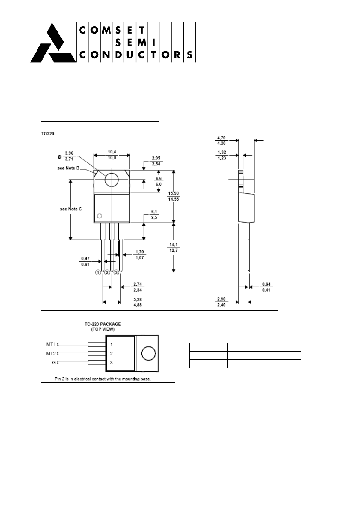
MECHANICAL DATA CASE TO-220
Pin 1 : Main Terminal 1
Pin 2 : Main Terminal 2
Pin 3 : Gate
Page 3 of 3
 Loading...