

Page 1
SEMICONDUCTORS
TIC216A, TIC216B, TIC216D, TIC216M, TIC216N, TIC216S
• 6 A RMS
• Glass Passivated Wafer
• 100 V to 800 V Off-State Voltage
• Max I
• Sensitive gate triacs
• Compliance to ROHS
DESCRIPTION
This device is a bidirectional triode thyristor (triac) which may be triggered from the off-state
to the on-state by either polarity of gate signal with main Terminal 2 at either polarity.
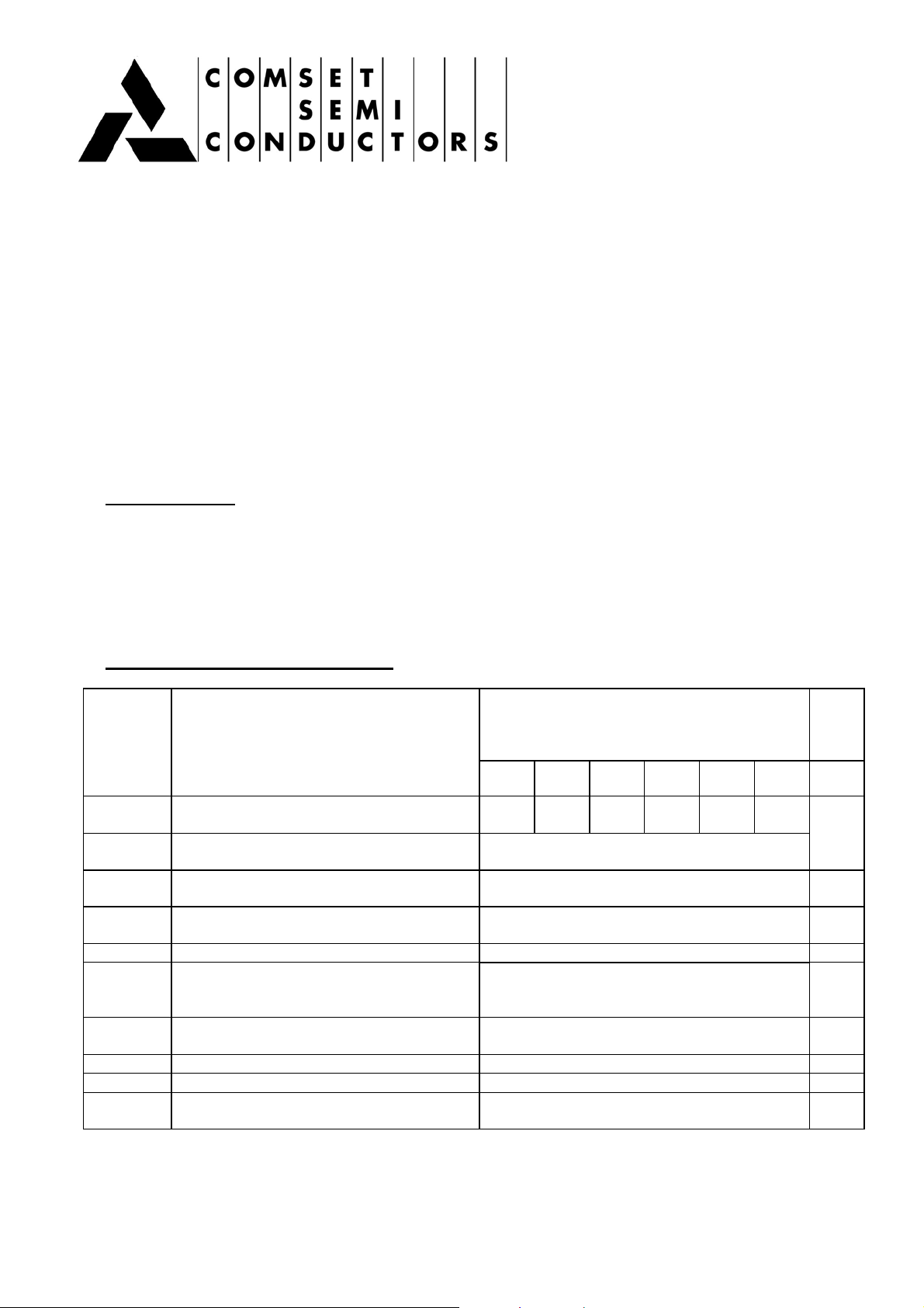
ABSOLUTE MAXIMUM RATINGS
SILICON BIDIRECTIONAL TRIODE THYRISTOR
of 5 mA (Quadrants 1-3)
GT
Symbol Ratings
V
DRM
I
T(RMS)
I
TSM
I
TSM
IGM
PGM
P
G(AV)
TC
T
stg
TL
Repetitive peak off-state voltage
(see Note1)
Full-cycle RMS on-state current at (or
below) 70°C case temperature (see note2)
Peak on-state surge current full-sine-wave
(see Note3)
Peak on-state surge current half-sine-wave
(see Note4)
Peak gate current ± 1 A
Peak gate power dissipation at (or below)
85°C case temperature (pulse width ≤200
µs)
Average gate power dissipation at (or
below) 85°C case (see Note5)
Operating case temperature range -40 to +110 °C
Storage temperature range -40 to +125 °C
Lead temperature 1.6 mm from case for 10
seconds
Value Unit
A B D M S N
100 200 400 600 700 800 V
6 A
60 A
70 A
2.2 W
0.9 W
230 °C
Page 1 of 3
Page 2
SEMICONDUCTORS
TIC216A, TIC216B, TIC216D, TIC216M, TIC216N, TIC216S
Notes:
1. These values apply bidirectionally for any value of resistance between the gate and Main Terminal
1.
2. This value applies for 50-Hz full-sine-wave operation with resistive load. Above 70°C derate
linearly to 110°C case temperature at the rate of 150 mA/°C.
3. This value applies for one 50-Hz full-sine-wave when the device is operating at (or below) the rated
value of on-state current. Surge may be repeated after the device has returned to original thermal
equilibrium. During the surge, gate control may be lost.
4. This value applies for one 50-Hz half-sine-wave when the device is operating at (or below) the rated
value of on-state current. Surge may be repeated after the device has returned to original thermal
equilibrium. During the surge, gate control may be lost.
5. This value applies for a maximum averaging time of 20 ms.
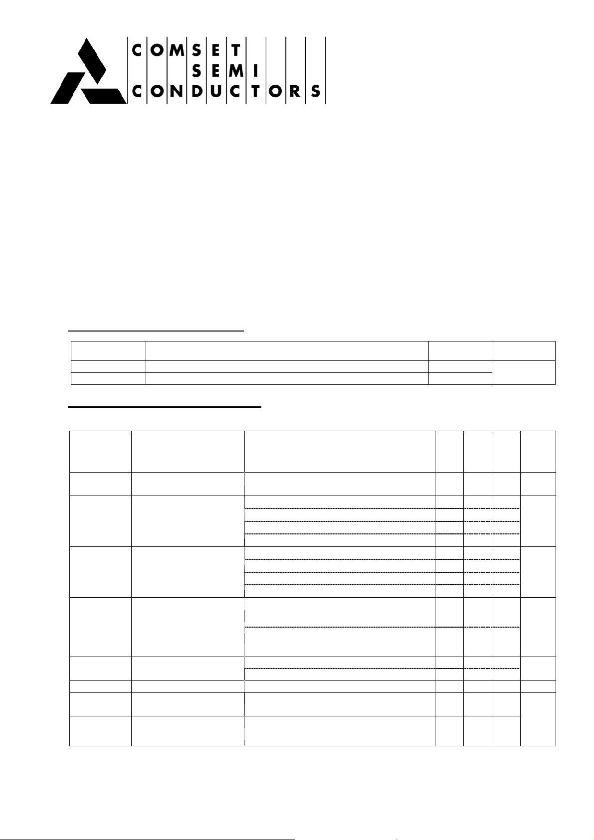
THERMAL CHARACTERISTICS
Symbol Ratings Value Unit
R
∂JC
R
∂JA
ELECTRICAL CHARACTERISTICS
TC=25°C unless otherwise noted
Junction to case thermal resistance ≤ 2.5
Junction to free air thermal resistance ≤ 62.5
°C/W
Symbol Ratings
I
DRM
IGT
VGT
IH
IL
VTM
dv/dt
dv/dt©
Repetitive peak offstate current
Gate trigger current
Gate trigger voltage
Holding current
Latching current
Peak on-state voltage I
Critical rate of rise of
off-state voltage
Critical rise of
communication voltage
† All voltages are whit respect to Main Terminal 1.
= Rated V
V
D
= 110°C
T
C
V
supply
V
supply
V
supply
V
supply
V
supply
V
supply
V
supply
V
supply
V
supply
initiating I
V
supply
initiating I
V
supply
V
supply
= ± 8.4 A, IG = 50 mA (see Note6) - - ±1.7 V
TM
V
DRM
T
= 110°C
C
V
DRM
T
= 70°C
C
Test Condition(s)
, , IG = 0,
DRM
= +12 V†, RL = 10 Ω, t
= +12 V†, RL = 10 Ω, t
= -12 V†, RL = 10 Ω, t
= -12 V†, RL = 10 Ω, t
= +12 V†, RL = 10 Ω, t
= +12 V†, RL = 10 Ω, t
= -12 V†, RL = 10 Ω, t
= -12 V†, RL = 10 Ω, t
= +12 V†, IG = 0,
= 100 mA
TM
= -12 V†, IG = 0,
= -100 mA
TM
= > 20 µs
p(g)
= > 20 µs
p(g)
= > 20 µs
p(g)
= > 20 µs
p(g)
= > 20 µs
p(g)
= > 20 µs
p(g)
= > 20 µs
p(g)
= > 20 µs
p(g)
Min Typ Mx Unit
- - ±2 mA
- - 5
- - -5
- - -5
- - 10
- - 2.2
- - -2.2
- - -2.2
- - 3
- - 30
- - -30
= +12 V† (seeNote7) - 50 = -12 V† (seeNote7) - -20 -
= Rated V
= Rated V
DRM
DRM
, IG = 0
, I
TRM
= ± 8.4A
- ±50 -
±5 - -
Page 2 of 3
mA
V
mA
mA
V/µs
Page 3
SEMICONDUCTORS
TIC216A, TIC216B, TIC216D, TIC216M, TIC216N, TIC216S
Note 6: This parameters must be measured using pulse techniques, t
contacts, separate from the courrent-carrying contacts are located within 3.2mm (1/8 inch) from de device body.
Note 7: The triacs are triggered by a 15-V (open circuit amplitude) pulse supplied by a generator with the
following characteristics : R
= 100Ω,
G
= 20 µs, tr = ≤ 15ns, f = 1 kHz.
tp(g)
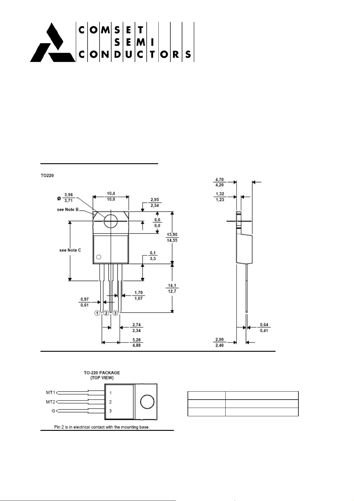
MECHANICAL DATA CASE TO-220
= ≤1µs, duty cycle ≤ 2 %, voltage-sensing
W
Pin 1 : Main Terminal 1
Pin 2 : Main Terminal 2
Pin 3 : Gate
Page 3 of 3
 Loading...