


,
~
.........
•
"'
J
'*
zao
S
INGLE
REFERENCE MANUAL
BOARD
SBC880
ro~t1PUTER
1
\ j
"'-
;. .
\.
.
,

•
Copyright
No
part
transcribed,
human
or
electronic,
o
the
r wi s e ,
8614
Hamilton
SUNTRONICS
respect
to
product
agreement.
revise
the
notify
this
content
any
agreement
(c)
1982
of
this
stored
computer
mechanical,
wit
Ave.
CO., INC.
the
it
describes
Further,
pUblication
hereof
person
to
the
publication
h0 u t
Huntington
contents
contrary
COPYRIGHT
by
COMPUTIME.
in
a
retieval
language,
magnetic,
the
exp
makes
of
is
SUNTRONICS
and
without
of
such
may
res
s wr
Beach,
DI
SCLAlMER
no
representations
this
manual
covered
to
m~ke
obligation
revision
exisits.
NOTICE
All
be
system,
in
any
optical,
itt
CO.,
changes
Rights
reproduced,
or
form
en
permiss
California
itself,
by
a
INC.
or
reserves
of
SUNTRONICS
changes,
.
Reserved
translated
or
chemical,
ion
92646
or
whether
warranty
from
Worldwide.
transmitted,
by
any
manual,
0 f ooMPUTI
U.S.A.
warranties
or
or
the
time
to
00.,
except
into
means,
not
repair
right
time
INC.
when
any
or
ME
with
the
,
to
in
to
an
i

•
SECTION
SECTION
SECTION
SECTION
I
GENERAL
II
FUNCTIONAL
I I I I
IV
NTERF
BOARD
SECTIONVDETAIL
APPENDIX
APPENDIX
APPEl·mIX
APPENDIX
APPENDIX
S~·
S
T'E1'Y1.
- A
- B
- C
- D
- E
l\DN I
USART-TIMER
USART
PROGRA\'l\W3LE
PARALLEL
INTERFACING
TOR
TABLE
DESCRIPTION
DESCRIPTION
ACES
OPTIONS
..............••••....•.
.•.....•.•.....••.....
DESCRIPTION
OF
CONTENTS
......•.........
............•
.•.••...•.•••••..•
AND
I/O
INTERVAL
PRINTER
NON-
••••••••••••••••••••••••••••••••
INSTALLATION.....
IEEE
DYNAMIC
ADDRESS
TII'rIER
Page
ING.
MEMORY
Number
1
3
5
9
11
15
19
27
31
33
35

•
NTRODUcrION
I
------------
The SBC880
is
compatible
contains
board
The
board
enough
system
conservatively
in
and
you
Before
with
for
EPROM
FEATURES
--------
An
on
by
8
Power-on
EPROM
of
location
In
provided
is
location,
tested
receive
installing
the
a
2708
then
board
static
may
64K
or
addition
not
used
SBC880
jump
optionally
(U23)
and
a
Processor
with
features
or
as
is
manufactured
rated
to
it.
features
EPROM.
refer
EPROM
RAM
is
more
of
are
to
the
it
can
and
total
Board
the
the
assure
the
If
to
Section
can
may
be
available
be
RAM.
the
EPROM,
be
the
of
2K
SECTION
GENERAL
is
IEEE
to
main
to
CPU
assure
that
board
and
you
want
V
be
addressed
used
used
Devices
2708,
located
static
bytes
DESCRIPTION
a
powerful
S100/696
allow
its
board
using
quality
long
the
board
read
this
options.
to
use
Board
on
in
place
directly
in
shadow
that
2716
an
ram
EPROMS
additional
on
is
of
ram may
any
I
bus
use
in
life.
will
manual
The
one
options
any"1K
of
to
mode
can
1K
used
Z80
based
standard.
as
a
a
larger
components
All
work
and become
board
of
for
or
the
the
EPROM
to
be
or
the
lK
boundary.
instead
be
present
design
The
stand
alone
system.
boards
are
properly
comes
the
configured
other
modifications.
2K
boundary.
EPROM
if
(or
allow
used
4118
of
the
in
static
If
at
on
the
static
the
the
the
SBC880
single
that
burned
familiar
type
desired.
RAM).
full
EPROM
ram
EPROM
EPROM
board.
which
are
when
of
A lK
The
use
RAM.
is
The
model
and
baud
board
rate
signals
terminal
connector(J1).
wit
h buf
is
occasionally
fer
connected
rib
bon.
be
selected
A
DMA
MWRT
under
Two
The
prgrammable
timer
A 4MHz
capability
signal
control
connector
is
available
is
equipped
is
programmable
required
equipment
Reverse
edt
ype de
needed
device.
crystal
for
2
generated
of
DMA
timers
output
J2.
for
and
A
use
vic
It
can
or
4
is
provided
on
logic
controls
parallel
at
with
by
by
terminal
may
channel
es
sue
as
a bUSy
sense
provide
MHz
operation.
the
or
are
connector
a
USART
means
be
connected
capability
has
things
s a I I s Ys t em
as
well
CPU
board
a
front
available
are
input
J2.
1
and
of
a
type
equipment
pr i nt er
or
ready
such
as
or
panel.
for
available
and
a
a RS232
interface.
programmable
is
directly
is
available
s.
Th
ere
indication
as
out
tim
a
means
of
elsewhere
use
by
user
at
the
parallel
timer.
provided
to
the
ve r
sec
from
of
paper
i ng
having
in
the
programs.
parallel
output
RS232
for
hanne 1
and
system
The
All
for
use
the
or
can
the
I/O
port

All
tor
stable
both
5-100
all
design.
sides,
on
bus
board
plated
sijnals
voltages
A
quality
are
through
fUlly
to
PC
holes
buffered
assure
board
and
is
gold
and
an
electrically
used
plated
regulators
with
contacts.
solder
are
clean
mask
used
and
on
2

-
FUNCTIONAL
SECTION
DESCRIPTION
II
Z80A
----
The
Z80
required
address
the
simp
A
bus,
timers.
for
clear
STATUS
------
The
control
by
device
and
access
acknowledgment
bus.
CPU
---
SBC880
microprocssor.
Z80. The 8BC880
1e jumpe r .
crystal
the
the
signal.
AND
---
status
a
DMA
control
is
to
bus
controller
Z80A
Associated
EPROM
CONTROL
-------
signals
device
and
memory.
is
requested
a
read
and
CPU,
and
and
for
single
and
a 8
reset
BUFFERS
-------
control
to
to
the
signal
The
write
bit
can
circuit
the
with
the
allow
The
duration
by
board
Z80
bi-directional
be
Baud
this
circuitry
8-100
DMA
activating
from
microcomputer
provides
to
memory and
run
provides
rat
circuit
buffers
bus.
a
transfer
device
the
at
of
CPU
either
timer,
are
which
interface
These
assumes
the
the
is
the
data
all
and
also
buffers
of
DMA
CPU
made
major
the
4
or
the
the
data
control
transfer.
DMA
available
designed
control
I/O
ports.
bus
are
2
MHz
timing
the
two
wait
generates
the
state
CPU
may be
between
request
around
sighals
A
16
generatedby
by
changing
for
the
SlOO
programmable
generator
a
power-on
status
tri-stated
the
DMA
on
thestatus
When a
signal,
on
the
DMA
8-100
the
bit
a
and
the
ADDRESS
The
CPU's
!2~!~
The
The
The
address
circuitry
devices
then
eight
or
devices
or
buffers
when
provide
Q~
data
data
I/O
8-100
I/O
the
data
BUFFER
buffer
sixteen
on
when a
~Q££~g
out
bus
out
output
when
data
input
are
CPU
address
the
CPU
transfer
the
address
buffer
signals
bus
will
cycles.
they
cycles
disabled
is
are
in
driving
is
a 16
board.
is
an8bit
only
The
transferring
bus
to
is
devices
during
bit
bits
The
of
data
for
from
contain
data
provided
data
tri-state
to
buffer
is
the
duration
tri-state
the
out
external
memory
to
the
3
the
to
CPU
valid
bus
data
to
to
the
write
data
buffer
8-100
is
occur.
of
buffer
the
data
will
to
CPU
to
out
bus
also
memory.
the
The
the
8-100
during
be
during
board.
or
I/O
buffers.
tri-stated
tri-stated
which
and
DMA
data
which
data
output
drives
to
device
transfer.
drives
out
memory
memory
The
The
other
by
will
write
by
read
data
cycles
data
the
DMA
the
bus.
DMA
in
~n

buffers
accessed
CPU
The
bu
memory
address
on
the
EPROM
----
The
EPROM
static
boundary
lK
BY
--
--
are
dlsabled
to
allow~t~
s.
decode
bits
board.
can
RAM
(4118
and
8 STATIC
-
------
and
the
selects
be
type).
optional
RAM
---
whenever
and
a
lK
device
control
the
(2708
The
ram
devices
being
circuitry
EPROM
type),
EPROM
can
on
accessed
or
static
2K
may be
be
selected
the
decodes
(2716
selected
CPU
to
R_~
type),
on
board
place
the
that
on
any
are
data
hig~
is
or
a
any
lK
boundary.
being
on
order
located
lK
lK
or
the
by 8
2K
The
type
lK
of
of
refresh.
diagnostic
of
the
SBC880
The
the
I/O
I/O
add
ports
ressbus
operations.
The
serial
interface.
USART
P~W3LE
------------
Two
8253
is
programmable
or
crystal
on-board
ram
This
provided
ram
tests
as
decode
on
the
I/O
The
baud
a
8251.
TIMERS
------
8254
timer
controlled
ram
may
on a
a
stand
and
control
t 0 de t e r
board
provides
rate
timers
can
clock
may
is
be
bad
be
static
used
dynami~
alone
circuitry
min
e w
are
asynchronous
is
provided
are
be
used.
oscillator
selected
to
ram
system.
hen
being
available
The
to
(2114
hold
type)
the
board
decodes
the
US
ART,
address
communication
by a
programmable
for
timers
on
the
any
stack
or
the
tim
for
use
are
board.
lK
boundary.
and
when
it
allows
lower
e r 0 r
input
on
the
clocked
requires
running
the
8
bits
par
or
via
a RS232
timer.
board.
from
The
no
use
of
a I I e I
output
The
An
the
An
8
bit
provided
circuitry
parallel
on
the
output
board.
(74LS373 and
port
The
and
ports
74LS374).
a 8
bit
parallel
are
4
implemented
input
with
port
TTL
are
type

•
EPRO:\1INTERF
The
EPROM
conditions:
1.
When
power-on
unconditionally
power
or
latch
and
set
(2708
through
compares
2.
When
memory
compares
the
ACE
will
power-on
on
the
is
the
tin
gs 0 r
type)
not
8131
be
selected
jump
latch
system
reset
address
the
the
15
to
address
using
read
operat
with
comparator)
SECTION
INTERFACES
for
jump
is
latch
enabled
is
selected
is
set
any
reset
button
when a memory
EPROM
the
bit
the
the
being
8131
SW3.
11
phantom
ion
EPROM
read
se 1e c t s
(U30)
For
through
is
per
switch
III
access
until
time
2K
option
formed
(I
set.
the
the
is
pressed.
read
·operation
compares
wit
ch SW3.For
compares
x 8
EPROM
15
to
(Q
settings
under
to
U
The
latch
system
the
to
wi
th
the
present)
EPROM
is
is
The
to
address
(2716
SW3.
R
present)
an
(as
following
and
U23
reset.
powered
power-on
is
performed
the
switch
1K x 8 E
bits
type)
and
address
detected
the
The
PRO
U30
that
is
up
M
10
a
by
The
EPROM
is
used
signal
CPU
WR!
tow
RA~
The
r i
ted
iss
EPROM
directional
through
directly
have
the
access
programs
boa
r d
can
even
PHANTOM
-------
When
only
pre
for
latch
when
the
selected
sse
all
dan
is
address
Likewise
on
latch.
data
from
reset
may
the
MEMRD
is
accessed
signal
a t a i n
e I ec
ted.
or
optional
data
the
data
access
S-100
the
EPROM
to
be
commun i
the
S-100
M:>DE
----
phantom
d
the
memory
set.
memory
I/O
input
Therefore,
an
I/O
operation.
optionally
signal
dur
is
jumpered
tot
he
bus
and
out
the
EPROM
bus
run
or
cat
in
optional
in
e
bus
EPROM
after
powe
read
r-
operations
During
external
and
the
device
The
be
ing
memory
to
RAMduri
RAM
only
bus
drivers.
or
operational
EPROM
wit
hat
is
completely
option
a
power-up
0 n I
at
this
output
program
into
EPROM
replaced
is
replaced
the
is
directly
appears
optional
~'1.
to
diagnose
e r
is
chi
time
to
the
cycles
memory
select
read
~~
ng
min
sse
that
a
in
by a 4118
by
and wr i
WE!
me
m0 r y wr i t e cyc I es w
input
MRQ
RAM.
so
te
operations.
to
connected
on
the
S-100
NOTE
condition
This
a I
R~~.
feature
a
and
that
It
failing
run
only
is
allows
d i ag
not
to
inoperative.
used
or
memory
board
when
1.
The
occur
are
the
EPROM
after
switch
(Q
to
R
the
EPROM
while
write
in
a
unaffected
can
a
power-up
can
cut)
system
wi
operation
normal
be
be
When
that
the
the
RAM
RAM
The
allow
to
bus
the
the
hen
the
CPU
indirectly
CPU
CPU
the
bican
necessary
suc~essfully
diagnostic
5-100
nos
the
bus.
tic
EPROM
t
The
est
reset
lIb
e seIec
the
power-on
ted
will
fashion.
by
the
power-
used
set
o.r
to
to
boot
syst"em
detect
to
s
is
is
5

the
by
the
into
starting
memory. A jump
the
8131
power-on
comparator.
data
in
memory
effectively
power-up
comparator
cannot
disappears
or
system
ad&tess
latch
is
to
is
select
now
reset
of
the
the
starting.
and
reset,
the
accessed
from
operation.
code
will
the
the
reset
EPROM
EPROl\l
in
a
system
that
address
because
normal
the
the
can
until
EPROM
will
then
power-on
not
be-accessed
Q
to
fashion
needed
program
be
·latch.
R
is
and
at
detected
open).
the
the
boots
When
(the
The
EPRQ;\l
next
A 1K x 8 b I 0 c k 0 f s
chips
com
When a memory
the
switch,
memory
(
low)
wr i
connected
accessed
available
U8ART
allows
bus
memory
board
diagnostic
scratchpad
run
signals
located
with
necessary
board
bus
RAM
ext
its
data
RA~
on
the
board.
paresaddres
comparator
the
C8/
ted
write
a t
a t a i n
the
operation
WE
to
directly
at
the
will
function
diagnostics
is
inoperative.
diagnostic
that
contains
programs
and
properly
on
in
no
RAM
data
i s a I
ernaIde
da t a i g
even
the
the
conflicts
if
your
is
accessed
in
bus
lowed
vic
nor
instead.
will
be
available
s
operation
detects
lead
/ in
to·
the
8-100
stack
8-100
same
receivers
t 0
erespondin
ed bY
When
taticRAM
The
RAM
bit
s
lOt
is
a
goes
is
put
s 0 f
the
CPU
RAM.
bi-directional
by
the
data
independently
to
be
An
example
on
the
the
can
operations.
if
the
bus.
address
between
system
during
sup
ply
the
boardan
your
to
i s imp I erne n
is
selected
hr0
performed
match
active
performed
the
The
CPU.
out
performed
of
board
balance
use
RAM
In
board
normal
space
the
uses
a
a
are
da
tad
g t·)
system
help
you
ted
u
by a 8131
ugh
1St
0
the
RAM
by
the
CPU
between
(low)
RAM
RAl'vl0nth
The
bus.
this
while
of
the
The
being
as
memory
full
memory
disabled
ire
the
by
use,
other
64K
the
at
the
CPU
chi
pst
data
RAM
The
on-board
of
the
the
feature
diagnosing
the
on-board
diagnostic
diagnosed
the
memory
devices.
of
read
and
c t 1Y
address
WR/
0 a I
e
boardis
bus
data
8-100
board
system
on-board
RAM.
operation
the
tot
the5amemem0rye
d
the
0 n-
boa
r d
RAM
get
is
inoperative,
your
system
singtwo
211 4
comparator
se
lee
t s
(MRQ
RAM
signal
and
would
chips.
low
is
~~~,
bus
when
be
a
dynamic
active)
and
the
is
the
CPU
d
ire
can
only
indirectly
EPROM
and
the
running
memory.
static
RAM
routines
was
affecting
RA\1
in
ycur
This
Whenever
will
the
the
on-board
he CPU. Th
yc 1e W 0 u1d have
RA:,l
w0 u 1d
the
on-board
going
again.
RAM
that
wit
ch.
and
RAM
When
active
c t 1Y
and
this
8-100
RAM
The
for
would
may
system
on-
8-100
static
usa
sup
ply
a
to
be
a
be
be
n
The
CPU
compares
and
looks
access
address
8131
to
comparator
select
I/O
address
is
I/O
devices
for
in
process.
devices.
the
are
bits
10RQ
to
Address
and
address
individual
selected
A3
be
The
through
active
CPU
bits
I/O
by an 8131
uses
bits
Ai
devices
6
A7
(high)
address
A3
through
and
on
to
the
indicating
A2
the
comparator.
I/O
bits
are
A7
are
decoded
AO
board
select
through
tested
as
The 8131
switch
that
with
follows:
an
A7
by
gates
I/O
to
the

RD
1-
0 1
1
0
1
0
1
0
1
0
1
0
1
0
1
0
-
Device
-~25!
"'11
" "
"
" "
"
"
"
Input
Output
Input
Output
tl
"
"
WR
A2
(f-
n-
0 0
0
0
0
1
0
0
0
1
0
0
0
1
1
0
1 0
1
0 1
1 0 1
1
0 1 1 0 8251
1 1
1
0 1 1
1
1
Al
n-
0 1
0
1
1
1 1
1
0
0
1
AO
(f-
0
1
0
0
1
0
0
1
0
I
1
Selected
fTmer---
tl
"
"
"
"
Port
Port
Port
Port
USART
"
tl
"
OQeratlon
Read-baue
Write
Read
Write
Read
Write
baud
counter
counter
counter
counter
Illegal
Write
Read
Write
Read
Write
Read
Write
Read
Write
mode word
input
output
input
output
data
data
status
control
rate
rate
1
1
2
2
port
port
port
port
register
register
registe'
register
time
time
The
I/O
final
select
through
selected.
active)
cycle
low,
aninput
selects
the
parallel
selected
8253
----
The
TIMER
-----
board
circuitry
8253.
for
the
transmit
timer
counter.
of
timer
a
32
bit
out
putsare
for
C
I/O
switch
A7
will
NOTE
a
different
(WR
active)
the
output
with
INTERFACE
---------
provides
to
Timer
zero
8251
and
zero
(GO)
The
two
counter/timer.
ava i IabI e
a
description
port
that
at
cyc I e s e
input
AO
high
the
count
is
USART
receive
is
output
(CS)
and
address
which
cause
for
operation
the
port.
and
or
a 2Mhz
used
and
clock
tied
of
the
for
of
for
determine
the
some
same
lee
t s
Adderss
output
low.
inputs
as
its
inputs
active
timer
two
The
use
the
8253
each
what
I/O
devices
devices
takes
address.
the
i n
bit
ports
clock
of
timer
a
programmable
output
of
(high)
one
(01)
timers
gate
ate
inputs,
0 nnec
functions.
device
during
place
put
AO
and
from
is
connected
the
to
can
is
state
on
than
When
po r
is
A2
t,
ignored
the
the
zero
and
baud
USART.
permanently
is
connected
be
used
count
torJ2.
determined
of
address
the
an
input
for
is
high
and
an
when
same
clock
timer
rate
directly
The
gate
together
inputs,
Re
fer
by
bits
board
to
cycle
an
output
and
Al
0 ut pu tcYc I e
accessing
devices
are
oscillator
one
of
generator
to
input
enable
to
to
the
and
to
Ap
pend i x
this
input
form
count
the
A3
be
(RD
is
the
the
to
8251A
-----
Tim
e r z e
the
transmit
Transmit
1489
a
of
the
by
a
1488
transmit
by
the
input
has
no
USART
-----
roo
data
RS232
USART.
Jl
1489
can
other
INTERFACE
---------
f
the
and
at
receiver
Transmit
RS232
pin
11
and
be
sensed
affect
8253 d i v
receive
the
RS232
and
data
transmitter
input
provided
as
on
the
idesthe2MH
clocks
connector
applied
(TXD)
to
at
the
RS232
to
the
a
status
operation
7
(TXC
to
from
J1
DSR/
bit
z c I 0 ck dow
and
Jl
pin
2
the
receive
the
US
pin
3.
The
connector
input
in
the
of
the
RXC)
is
ART
of
status
USART.
nan
to
level
data
is
level
reverse
is
level
the
USART.
register
This
d
provide
the
shifted
input
shifted
channel
shifted
allows
s
USART.
by
(RXD)
This
and

programs
I/O
devices.
to
permanently
the
RS
232 i nt erface i 5 a Iway s
partusedfor
will
functional
not
be
description
sensea
The
at
the
the
used
nott-rpady
CTS/
input
input
of
USART wi I I
on
the
of
the
or
buffer
of
the
rea
be
board.
USART
the
USART
USART.
dy
tot
full
This
cond
is
tells
ransmit
it
tied
dat
ions
active
the
a.
on
USART
Theact
an 8 251A 0 r 9 551.The0Ide
Refer
to
Appendix
B
device.
ser
(low)
r 8
for
ial
that
ua I
2,5
.
1
a
The RS232
device
connected
RS232
the
4
and
connector
connector.
5.
Carrier
BAUD
----
When
s e
16
I e c
times
RATE
----
the
tedthat
divisors
application.
connector
without
device
Data
detect
DIVISORS
--------
baud
the
will
Baud
---9600--
4800
1200
modems.
will
jumpers
Request
terminal
Pins
rate
wi I I d i v
baud
rate
be
Rate
2400
600
300
150
110
is
configured
be
to
ready
6,
8
timer
ide
desired.
of
help
Any modem
satisfied
together
send
is
is
and
20.
is
initialized
the
2MHz c 10 c k t 0 a f r e
in
to
allow
by
the
jumpered
jumpered
The
following
selecting
Divisor
-----13
26
52
104
208
417
833
1136
direct
signals
jumpers
following
to
to
required
on
RS232
Clear
Data
a
divisor
list
the
connection
the
board.
signals
to
send
set
ready
must
que
nc y t
of
baud
one
for
by
hat
to
the
The
at
Pins
and
be
rate
your
a
i s
The
parallel
triggered
and
need
register
latched
This
during
The
clock
an
parallel
transparent
da
tad
ire
por
tis
the
latch
low
(input
the
CPU
the
I/O
output
register.
no
additional
is
provided
at
the
will
I/O
output
input
latch.
c t I y
se Iec
tedduri
inputs
port
data
bus.
connector
rising
transition
tot
he
when
selected)
The
J2.
port
The
cycle.
port
The
CPU
ng
is
register
buffering.
to
the
(low
every
is
tri-state
b i - d
the
the
latch
will
latch
implemented
outputs
The
I/O
to
connector
high)
time
implemented
buffers
ire
c t
ion
I
/0
in
put
select
be
latched
strobe
8
are
clock
transition
the
a I da
cyc
strobe
signal
with
buffered
J2.
output
with
on
tab
Ie.
Th
and
is
to
a
this
u s w
e da
goes
then
made
a
74LS374
the
Output
of
port
74LS373
chip
hen
tap
from
presented
available
on
the
output
this
is
selected
the
resentat
edge-
chip
port
data
clock.
octal
provide
i n
put
high
is
to
to
at

•
(':,.
«-
SECTION
IV
OPTION1ON
------
-
--
The SBC880
follows:
l.
Z
2.
Y
3.
F
to
4.
H
5.
J
6.
L
7.
P
8.
P
9.
L
10.
H
1l.
V
to
12.
X
OPTION
------
TI
3
Voltage
1 •
2.
3 . J
4.
5.
6.
7•
8.
9 • V
10.
11.
12.
13.
2
-
-
F
to
H
to
to
L
P
to
P
to
L
to
H
to
to
X
to
y
to
Z
to
Sw
BOARD
-----
comes
K
to
to
G
G
to
to
K
to
M
to
0
to
N
to
K
to
M
W
V
to
2716
EPRQ\1
G
K
to
M
0
N
K
M
W
V
G
K
i t c h
open
open
shorted
I
shorted
shorted
open
shorted
open
open
open
shorted
open
EPRQ\1
shorted
I
shorted
shorted
shorted
open
shorted
open
open
shorted
open
open
open
6
EPROM
-----
etched
of
SW3
BOARD
-
2708
for
closed
the
OPTIONS
EPROM
2708
EPROM.
1
nte
1 . F
2.
3. J
4.
5.
6.
7
.•
8 . H
9.
10.
11.
12 . Z
13.
14.
The se
+5
I
to
H
to
to
L
to
P
to
0
to
L
to
to
V
to
X
to
Y
to
to
Sw
itch
G
to
defaults
vo
I t
G
open
1
shorted
K
open
open
M
open
0
N
shorted
K
shorted
1\1
shorted
W
shorted
V
open
open
G
K
open
6
+5
EPRQ\1
SW3
of
are
closed
as
OPTION
------
10.
1l.
12.
l.
2 .
3.
4.
5.
6 •
7.
8.
9.
3
-
-
F
H
J
L
L
H
P
p
V
X
y
Z
4118 RA.\i
G
to
to
to
to
to
to
to
to
to
to
to
to
open
1
shorted
K
open
M
open
K
open
M
shorted
a
shorted
N
open
W
open
V
shorted
G
shorted
K
shorted
substituted
for
9
EPRO:\1

OPTION
------
An
EPRO~
board
Phantom
1.
2.
4 -
Power-on
- - "
is
must
etched
mode
T
to
Q
to
be
as
U
shorted
R
shorted
Jump
present
for
follows:
the
~
no
'tt_
to
2708
Phantom
use
the
EPROM
Mode
power-on
and
the
jump
power-on
feature.
jump
with
The
no
Q~I!Q~
~
The Eprom
1.
2.
Q~I!Q~
The
~
EPROM
1.
2.
OPTION
------
To
7 -
-
disable
1.
2.
Q~!!Q~
This
~
option
-
Power-on
must
T
to
Q
to
-
No
or
T
to
Q
to
No
address
Q
to
T
to
-
l\IWRT
be
U
shorted
R
open
Power-on
optional
U
open
R
shorted
EPROM
R
open
U
open
genera
is
etched
Jump
present
RAM
selection
ted
on
with
Jump
the
to
may
by
Phantom
use
this
be
used
of
the
CPU
board.
Mode
option.
with
EPROM
this
entirely.
option.
1.
2.
Q~!!Q~
1.
2.
Q~!!Q~
1.
2.
C
D
~
C
D
!Q
C
D
to
to
-
MWRT
to
to
-
to
to
E
shorted
E
open
E
open
E
open
MWRT
E
open
E
shorted
generated
generated
by
by
external
CPU
and
10
devices
external
devices

•
SECTION
DETAIL
DESCRIPTION
V
-Refer
each
ADDRESS
-------
The
During
(ADDSB/) low
can
DATA
----
During
is
74LS241
disable
DATA
----
to
functional
BUS
---
address
DMA
then
IN
BUS
--
---
memory
received
the
1.
EPROM
2.
On-board
3.
Programmable
4.
Parallel
5.
Memory
OUT
---
the
bus
operations
to
place
and
type
data
BUS
---
SBC880
block
of
tri-state
its
read
driven
device.
in
or
optional
static
1/0
write
schematic
that
the
own
address
or
I/O
Circuitry
buffers
timer
port
or
CPU
the
the
input
to
ram
ram
selected
1/0
while
follows.
is
buffered
DMA
the
under
selected
output
device
address
on
operations,
CPU
selected
selected
reading
using
will
bus
drivers.
the
bus.
bi-directional
is
provided
the
following
operation
the
74LS241
drive
the
S-100
(l/2
conditions:
in
progress
de"scriptions
devices.
S-100
The
data
data
of
pin
DMA
bus
7420)
of
22
device
in
bus
by a
to
Th e
CPU
bus
by 74LS241
the
operations.
bus
This
~L~
STATUS
------
Status
provided
device
bu f
Control
bus
may
control
the
signals.
as
the
system
MWRITE
to
may
CPU
wi I I dr i
will
device
SIGNALS
-------
fer
by
drive
other
you
CPU
disable
be
disabled
b i - d
to
A
disable
to
signals
to
the
may
one
received
contains
signal,
drive
to
a I
signals
section
pin
of
the
half
This
boardis
the
ire
c t
type
devices
DMA
ve
pin
place
SM1,
S-100
low
PSYNC,
19
bus.
of
buffer
it
a 1way s
then
buffer
by
ion
a I da
buffers.
on
device
23
(DODSB/)0nth
the
data
data
SMEMR,
bus
pin
the
(C/CDSB/)
another
18 (STATDSB/)
DMA
PWR/, and
of
a 8097
The
the
8097
may be
has
you
on
the
STATDSB/
tabusis
The
the
wishing
out
on
the
by
a 8097
de
vic
type
low
MWRITE
buffer
controlled
this
the
may
sour
device
the
buffer
cut
board.
buffers
S-100
to
buffers
bus.
SIN?,
e
PDBIN
to
signal
ceo
that
the
signal
dr I ve n
bus
transfer
e S- 100
on
SOUT, SINTA,
type
low
tog
tri-state
a
disable
is
that
in
permanently
f
the
is
etch
If
desired,
when
provide
during
the
tri-state
to
inc
are
provided
was
several
M\\"R
to
between
tot
provided
he S-100 da
write
memory
data
bus
tri-stat
0 n t r 0 I 0 f
buffer.
this
used
be
a
D~iA
board
I
TE
the
the
on
to
buffer
by
ways:
enabled
s igna I• I f you r
points
device
data
the
data
a
lowstat
and
allow
and
source
MM~ITE
buffer.
the
to
A
DMA
to
the
the
SWO/
the
the
and
control
The
so
C
is
tao
ut
from
write
out
the
are
A
D7.1A
status
bus.
S-100
device
gain
bus
by
board
that
of
the
and
buffer
~sing
e.
E
11

the
poi
E.
bus.
n t s
This
provided
or
a
signal
floatin
control
signal
Can
option
g
of
is
This
d E~a n
the
the
the
left
option
dotIien
requires
MWRITE
with
MWR
ITE s i g na
bus.
floating.
the
is
signal
same
Data
ins
that
enabled
tal
lin
that
timing.
Ion
in
memory
g a j um
the
is
the
by
cutting
DMA
enabled
This
S
-100
may
per
device
by
is
bus
be
the
bet
weenpoi
hav~
the
STATDBS/
necessary
wh i
let
overwritten
etch
between
n t s 0
a
buffer
signal
to
prevent
ransferrin
if
and
to
g
this
The
signal
active
RD/
w
hen
and
the
MWRITE
(low)
(low)
OTHER
SINTA
the
CPU. SWO/
any
input
indication
SWO/
inactive
SX
TRQ
/ i s
required
transfers.
at
the
CONTROL
-------
The
goes
signals
active
device
PSYNC
valid
developed
IEEE
CPU
S-100
memory
active
memory
is
being
RD
/ i
sac
PHLDA
CPU. Th
th~
requesting
of
the
signal
DMA
only
device
goes
point
properly.
SOUT
(low)
IORQ/
s i g na 1s
is
active
at
the
at
the
STATUS
goes
active
cycles.
that
is
active
(low)
not
by
SHLTA
CPU.
SIGNALS
-------
when
signal
I/O
by
specification.
(low)
read
acknowledged
t i v e
goes
iss
i g na I a c k
bus.
BUSRQ/
active
in
its
PHLDA/
is
active
at
the
CPU.
are
active
RD/and
(high)
CPU.
SMl
CPU.
SIGNALS
(high)
goes
active
This
a
write
(low)
will
ge n
era
ted
the
CPU. SXTRQ/
goes
OUTPUT
------
PSYNC, PWR/
(low).
the
goes
or
memory
a
flip
refresh
at
of
I/O
(low)
active
C/CDSB/
device
active
flop
cycles.
the
input
at
(high)
now
device
The
CPU
going
drives
active
the
when
operation
is
always
SINP
(low)
when
goes
when
signal
or
when
be
active
by
active
and
wants
(high)
cycle.
and
The
CPU.
cycle
(SINTA
the
when
1e dge s a
with
generates
S-100
BUSRQ/
where
(high)
is
at
when
active
the
MREQ/are
signals
active
Ml/
(low)
when
output
RD/
is
(high)
the
boa
is
(high)
PDBIN
will
to
momentarily
The
produces
PSYNC
PWRl
The
RC"~S
si;r-al
is
in
high).
CPU 0 r w
BUSAK/
DMA
the
highest
this
(low).
BUSRQ/
signal
has
gone
a
driven
WR/
CPU.
active
(high)
and
the
is
used
cycle
inactive
r d b ec a
used
when
are
be
driven
take
timing
signal
active
process
PDBIN
hen
r e
signal
PHOLD/
active
DMA
and
cannot
and
(high)
SMEMR
WR/
and
when
IORQ/
CPU
to
is
at
the
use
to
request
HLTA/
tri-stated
control
timing
is
PDBIN
is
S I
NTAisac
goes
questan
priority
goes
active
access
IORQ/
(low)
go
is
provide
going
(high)
0 n I y 8
low
at
for
as
not
(low)
goes
or
active
active
in
active
and
be
when
is
MREG/
Ml/
active
not
to
CPU.
goes
when
by
of
the
this
defined
produced
when
active
when
din
may
response
(low).
the
can
tri-stated.
signals
the
signals
active
at
the
are
goes
(low)
performing
an
take
or
SINTA
The
bit
da t a i s
16
bi
active
C/CDSB/
a
DMA
the
bus.
start
signal
WRi
an
interrup~
(high)
t i
ve
(low)
d i
cat
est
take
(low)
CPU
be
perfomed
are
(high)
CPU.
active
active
at
early
place.
signal
t
data
(low)
type
The
of
any
by
the
during
goes
when
when
(h
i g
h).
at
the
hat
control
to
the
when
BUSAK/
is
at
is
is
a
a
a
12

CONTROL
-------
SIGNALS
-------
Ir?UT
-----
The
because
signal
IEEE
only'S
SIXTN/
access.
this
will
EP~1
one
wait
is
access
being
cycles
panel
goes
active
(low)
input
bus,
signal
make
wait
clock
state
normally
cycle
accessed
(wait
type
active
(low)
atthe
to
the
non-maskable
d r iven
active
devices
DMA
---
active
(low)
to
CONTROL
-------
5-100
Since
is
the
state
cycle
generator
used
devices
(high),
CPU.This
the
signal
request
LINES
-----
bus
bit
is
a
response
a
16
bit
ignored.
WAIT/
generator
during
by
by
inserting
holds
states)
to
WAIT/
at
the
S-100
CPU. When
NMI/
interrupt
(low)
at
a t
the
access
signal
accesses
access
The
signal
accesses
must
slow
PRDY/
desired.
halt
is
one
NMI/
goes
request
the
CPU. r
signals
can
be
memory
wait
active
or
goes
bus,
of
is
active
5 - 1 0 0
he
to
the
5IXTN/
are
to
a
is
never
go
active
make
to
enabled
states
XRDY
single
active
the
the
driven
input
bUS,
PHOLD/
bus.
is
required
request
XRDY
the
the
on-board
by
or
I/O
(low)
is
step
(low).
signal
maskable
active
(low)
to
the
signal
not
requested
or
(low)
WAIT/
at
for
normally
for
PROY
a
jumper
devices
the
the
When
INT/
used
by'
a
when
at
signal
EPROM.
CPU.
the
number
processor.
by
the
16
by
the
option.
to
used
PINT/
will
the
CPU.
bit
the.
driven
active
The
extend
The
is
be
interrupt
at
the
(low)
the
CPU
at
the
CPU.
This
When PHOLD/
s i gn a I BU5RQ/ wi I I
is
used
by
board
~emory
board,
CPU.
EPROM
PRDY/
device
of
clock
by
front
PWAIT/
driven
active
request
S-100
is
the
The
low
The
for
an
the
is
be
DMA
The
operations
states
AD05B/
active
5MEMR,
may
C/CDSB/
active
primary
the
tri-states
(low).
5M1,
be
tri-stated
tri-states
(low).
are
PHLDA s i g na I
I:X\1A
control
SYSTE\l
------
A
positive
51.
The
the
places
at
on
are
A
positive
voltage
regUlator
should
POWER
-----
This
regulator
+5
volt
around
S-100
the
board
decoupled
be
voltage
bus
is
is
present
lines
0005B/,
data
STATDSB/
SImA
When
going
signals
LINES
-----
8
volts
is
output
the
pin
to
with
16
volts
regulated
decoupled
used
out
bus
the
and
by
the
a
DMA
active
and
DC
is
regulated
decoupled
is
board.
52.
The
develop
1.5
DC
on
S-100
to
tri-state
AD05B/,
drivers
address
tri-states
SWO/
when
STATD5B/
signal
device
(h
drive
should
on
decoupled
A
negative
voltage
-12
volts
uf
capacitors
should
on
the
by
a
bus
5TATD5B/,
when
bus
drivers
the
it
is
if
selected
PSYNC, PWR/
is
granted
i g
h)
i t
wi
its
own
be
present
on
the
its
input
by
.1
16
is
regulated
and
at
be
present
1.5
board
uf
pins
to
capacitor
50
the
and
it
is
status
driven
I I
signals
on
board
by
uf
volts
-5
thier
at
develop
and
bus
drivers
C/CD5B. OOD5B/
driven
when
signals
active
by
a
jumper
and
POBIN
access
nor
rna I I Y 8 C t i
on
to
5-100
to
a
1.5
bus
develop
uf
capacitors
DC
should
by
two
volts.
Both
inputs
8-100
bus
+12
at
its
53.
active
it
is
SOUT,
(low).
when
to
the
vat
the
bus.
pins
+5
capacitor
at
be
regUlators
regUlators
and
pin
volts.
input
for
DMA
tri-
(low).
driven
SINP,
MWRITE
option.
driven
bus
e
the
1
and
volts.
and
various
present
outputs.
2.
This
The
and
by
a
13

SYSTEM
------
The
board
oscillator.
flop.
the
the
The 2
clock
The
CPU
S-100
MHz
is
CLOCK
-----
generates
2/4
and
bus
clock
always
The
MRs
related
at
is
2
4
MHz
jumpers
02.
provided
MHz
all
timing
clock
circuitry.
An
inverted
and
is
is
selects
directly
not
from
divided
which
The
version
affected
a 4
selected
to
S-100
MHz
down
clock
of
by
crystal
to
rate
clock
02
bus
the
2
is
provided
as
2/4
controlled
MHz
is
is
provided
CLOCK/.
MHz
by a
applied
~s
jumper.
flip
to
to
01.
This
~!~!§M
!!~~~!
When PRESET
capacitor
driven
signal
is
then
1.
2.
3.
4.
The
reset
released
takes
circuit
during
on
low
is
synchronized
applied
The Z80
The 8251
POC
The
for
to
charge
de-bounces
power
!:~£!:!QNS
is
driven
by
this
the
to
line
system
the
following
CPU
USART
at
the
S-100
power-on
signal
jump
will
approximately
the
100
the
up.
active
is
discharged.
reset
to
the
bus
latch
remain
uf
capacitor
reset
(low)
button
system
circuits:
active
470
milliseconds
switch
at
clock
(low)
to
and
the
This
being
a
provides
S-100
signal
pressed.
with
~fter
due
true
bus,
a
flip
the
to
level.
a
is
The
switch
the
This
reset
a
100
normally
PRESET
flop
and
time
same
signal
uf
is
it
14

Swi
tch
SWI
-
selects
US
ART
the
TIMER
base
APPENDIX
AND
address
I/O
A
ADDRESS
range
of
ING
8
addresses
RANGE
-----
00-07
08-0F
10-17
18-IF
20-27
28-2F
30-37
38-3F
40-47
48-4F
50-57
58-SF
60-67
68-6F
70-77
78-7F
80-87
88-8F
90-97
98-9F
AO-A7
A8-AF
BO-B7
B8-BF
CO-C7
C8-CF
DO-D7
D8-DF
EO-E7
E8-EF
FO-F7
F8-FF
SWl
SW2
X
X X X X
X X
X
X X
X
X
X
X X X X
X
X X
X
X X X
X X
X X
X
SW3
X X X X
X X X X
X
X X X
X
X
X X X
X X
X
X
SW4 SW5
X X
X X
X X
X X
X
X X
X
X X
X
X X
X
X
X
X
X
X
X
X
X
X
X·
X
X
First
2nd
3rd
4th
5th
6th
7th
8th
address
"
"
"
"
"
"
"
XO
Xl
X2
X3
X4
X5
X6
X7
or
or
or
or
or
or
or
or
X8
X9
XA
XB-
XC
XD
XE
XF-
- Timer
-
"
"
tl
Parallel
-
-
"
-
USART
"
o
Data
1
2
Control
Data
Control
15
"
"
Input
"
and
"
Ou
tputPort
"
"

SWI - 5
SWI -
SWl - 3
SWl - 2
SWl - 1
------
4
~j
~~
-
[~~~~~~
[~~~~~~~~
---Sase
-~I/O
Address
PorI
Seleelion
Seleelion
A2
Al
--------------------------------------
Timer
"
"
"
Parallel
II
US
ART
"
0
Data
1
"
2
Control
"
I/O
"
Data
Control
0 0 0
0 0 1
0 1
0 1
1
1
1
1 1 1
0 0
0
1
AO
0
1
1
0
16

Pin
---
No
--
-
.
TABLE
1
CONNECTORJlSIGNALS
Function
--------
11
20
PIN
---1--
10
11
12
14
15
16
17
18
19
20
21
22
23
24
25
2
3
4
5
6
7
8
2
3
4
5
6
7
8
9
NO
RS232
RS232
Requestto
Clear
Data
Signal
Carrier
Reverse
Data
TABLE
CONNECTOR
FUNCTIONS
--Output-Port
Counter
Transmit
Receive
to
Set
Ground
Detect
Channel
Terminal
2
J2
SIGNALS
Output
Output
Output
Output
Output
Output
Output
Signal
Output
Counter
Counter
InDut
In~ut
ln~~t
Input
Input
Input
Input
Input
Port
Port
Port
Port
Port
Port
Port
Port
Signal
Input
Port
input)
Counter
Send
Send
Ready
Port
Port
Port
Port
Port
Port
Port
Ground
Port
1
Gate
2
Gate
Data
Data
Data
Data
Data
Data
Data
Data
Ground
Strobe
1
Output
2
Output
Data
Data
Transmit
Ready
Data
Data
Data
Data
Data
Data
Data
Data
Clock
Input
Input
Bit
Bit
Bit
Bit
Bit
Bit
Bit
Bit
Bit
Bit
Bit
Bit
Bit
Bit
Bit
Bit
(also
0
1
2
3
4
5
6
7
0
1
2
3
4
5
6
7
counter
2
17

•
TH I S PAGE
LEFT
BLANK
18

-
APPENDIX
USART
8251
or
B
9551
computer
The
tasks:
1.
Output
2.
Input
3.
Outputs
4.
Inputs
Control
they
USART.
The
monitoring
conditions,
codes.
or
control
INITIALIZATION
--------------
The
s
tar
following
following
operations.
which
codes
are
status
Program
USART
tin
g a
it
used
the
when and how
signals
may be
new
power-up
completion
Following
can
program
control
status
data
data
determine
to
register
USART
logic
initialized
se
neither
controlling
codes
to
be
that
set
or
contents
operation
may
may
be
ria
1 I
and
of
a
transmit
transmitted
has
been
the
mode
reset
read
be
used
/0
subsequently
one
reset,
data,
based
to
following
seq
ue nc e •
activity
the
nor
the
USART
received
the
control
will
in
write
on
request
and
USART
receive
performs
USART
signals
be
order
reading
interrupts.
a
system
The
may
preceeding
enters
data.
the
will
read
to
data
USART mus t be
be
opearate
output
by
determine
or
output
status
reset
reset
an
the
bit
or
at
a new
idle
following
in
and
by
the
program
error
control
levels,
prior
res
any
time
set
state
to
e t
of
in
The
USARTis
from
needed
mode
a cornnand.
the
to
control
ASYNCHRONOUS
C/O=1
C/D=O
[~
FIGt~E
i
nit
i a
liz
ed
wit
processor.
initialize
is
Figure
followed
the
1
USART
by
OPERATION
1\DOE
--~~---
CONTROL
DATA
1.
Control
-
1
~~~~~~~NG
Word
h
two,
shows
one
or
Sequence
19
t hr ee 0 r f 0 ur
the
sequence
for
synchronous
two
SYNC
SY~~CHP.oNOUS
r-----------
1\1ODE
SYNC#1
SYNC#2
(OPTIONAL)
DATA
for
Initialization.
con
of
control
operation,
characters,
OPERATION
CO~~TRO
t r 0 I w0 r ds
words
the
and
then
INITIALING
SEQUENCE

Only
command
logic
proper
Following
as
operation,
mode
characters.
For
out
subsequent
commands.
anticipating
signal
a
internal
destination
a mode
byte)
either
put
or
single
bytes
a
reset,
control.
then
output
asychronous
a
sac
byte
There
following
-
address
and
to
the
0 nt r 0 I
output
are
a
mode
SYNC
the
based
the
If
next,one
as
control
two
control
an
is
character
chip
on
first
the
or
synchronous
cod
e i
as
ways
internal
set
directs
the
control
mode
or
codes
sin
control
in
input;
aside
bytes.
control
sequence
control
two
bytes
will
t e r
pre
which
Following
reset
for
code
codes
control
command.
mode
For
in
which
output
specifies
(as
be
operation,
ted
control
this
interpreted
a
are
to
information
it
is
determined
the
sac
interpreted
logic
an
may
external
bytes,
be
possible,
to
is
received.
interpreted
synchronous
by
as
SYNC
next
0
mm
and.
return
reset
its
the
byte
AI I
as
to
The
Control
asynchronous
and
relationship
transmitter
or
or
the
USART
code
1
specifies
transmitted
every
mode
BIT
of
NO
--O,r-
2,
3
4
5
6
interprets
clock
64th
operation
mode cod.; s
bits
operation
between
clock
DESCRIPTION
-OO-~-SYNC-M)DE
0
asynchronous
rate.
on
every
pulse.
00
01
10
11
0
1
0
1
0
1
5 BITS
=
6 BITS
=
7
=
8 BITS
=
PARITY
=
PARITY
=
ODD
=
EVEN
=
SYNDET
=
SYNDET
=
and
as
1
is
specified.
data
Asynchronous
check
synchronous.
BITS
PARITY
PARITY
determine
transfer,
pulse,
A
zero
PER
CHARACTER
PER
CHARACfER
PER
CHARACTER
PER
CHARACTER
DISABLE
EN..WLE
OUTPUT
INPUT
as
shown
whether
A
non-zero
operation
baud
serial
on
in
both
rate
every
bits
in
data
Figure
synchronous
value
and
16th
defines
and
may be
clock
0
and
2
and
in
receiver
received
pulse,
1
defines
bits
3.
or
0
the
or
For
determine
data
synchronous
character.
7
the
0
1
FIGURE
and
number
2
SYNC
=
1
SYNC
=
2.
Synchronous
asynchronous
of
data
CHARACTERS
CHARACTER
Mode
modes,
bits
which
20
Control
control
will
Code
be
bits
present
2
and
in
3
each

-
For
whether
whether
mo
bits,
11/2,
differs
Control
stop
specified
cases,
pUlses,
s ynch
as
data
synchronous
de a cha
bits
In"
synchronous
ron
internal
specified
stream
BIT
--0,1-
there
odd
or
rat
e r
an
optional
or
2
trailing
for
synchronous
code
the
respectively.
bits
will
with
half
i za t
NO
ion
synchonization
by
in
and
asynchronous
will
mode,
order
DESCRIPTION
-OO-~-TNVALID
be a
even
trail
01
10
11
parity
wiIleonsis
parity
stop
6 and 7
each
a
16
x
stop
wi I I be a
control
control
to
ASYNC
=
AS
=
ASYNC
=
bit
YNC
parity
bits.
or
in
or
is
bit
establish
modes,
bit
in
will
t 0 f f i
bit,
asynchronous
asynchronous
data
64 +
will
chi
specified,
M:>DE,
r-DD
MJDE,
be
ve,
a
preceeding
Interpretation
unit.
baud
be
bits
7,
6
eve
d. W
must
synchronization.
1
16 x
E,
64
adopted.
equivalent
and
x
X
bit
each
11/2
rate
henSYNDETis
one
be
BAUD
BAUD
BAUD
character,
six,
modes.
7
detected
s
mode
stop
factor.
determine
or
RATE
RATE
RATE
Thus
two
4
and
in
eve
nor
start
of
subsequent"
determine
bits
In
to
8
how
SYNC
at
the
FACTOR
FACTOR
FACTOR
5
determine
and
if
synchronous
e i gh t da t a
bit,
or
plus
how
can
only
these
32
clock
character
an 0 ut
characters,
head
so,
1,
bits
many
be
two
put
of
,
a
a:>M'MND
-------
Command
USART
SYNC".
during
to
be
the
format
2,3
4
5
6,
7
FIGURE
\\DRDS
-----
words
such
Consequently,
the
initiated
are
as,
execution
for
the
::;;
00
01
=
10
=
11
=
a
=
1
=
a
=
1
=
00
=
01
=
10
=
11
=
used
"reset
within
BITS
5
BITS
6
BITS
7
BITS
8
PARITY
PARITY
ODD
PARITY
EVEN
INVALID
1
1
2
3.
of
command
PARITY
STOP
1/2
STOP
Asynchronous
to
all
command
a
program
the
PER
CHARACTER
PER
CHARACTER
PER
CHARACTER
PER
CHARACTER
DISABLE
ENABLE
BIT
STOP
initiate
error
words.
BIT
BIT
Mode
specific
flags"
words
in
whict
communication
Control
or
may
functions
"start
be
specific
circuit.
Code
issued
within
searching
at
functions
Figure
the
for
anytime
are
4 shQws
21

BIT
NO
---
--
o 0 =
1
2
3
4
5
6
•
DESCRIPT
--fxEN-----
1 =
DTR
1 =
RxE
o =
1 =
SBRK
o =
1 =
ER
1 =
RTS
1 =
IR
1 =
ION
DISABLE
ENABLE
DTR
OUTPUT
DISABLE
ENABLE
NORMAL
TxD
IS
RESETS
STAUS
Rfs
REGISTER (PE, OE, FE)
OUTPUT
RESET
TRANSMISSION
TIL~SMISSION
IS
FORCED
RxRDY
RxRDY
OPERATION
FORCED
ALL
LOW
ERROR
IS
FORCED
FLAGS
FORMAT
TO
TO
0
IN
0
7
Bit
0
of
transmission
in
the
command
T x E
Bit
bit
used
accept
Bit
to
signal
ant
1
is
is
to
or
2
is
enable
set,
advise
from
complete
does
not
however.
characters
the
Receiver
error
overrun
(OE)
error
R x E.
EH
1 =
FIGURE
the
command
from
the
register.
T x
RDY
combine
the
Data
The
Terminal
DTR
a modem
transmit
the
Receiver
the
R x
data.
RDY
being
character
inhibit
the
Consequently,
will
be
Character
will
probably
is
usually
ENTER
4.
word
USART
Figure
to
output
that
Enable
output
generated
is
framed
assembly
if
assembled
Buffer.
be
reset
HUNT
l'vDDE
Control
is
the
transmit
cannot
5
defines
take
control
Readv
(DTR)
con'nection
th~
date
Command
signal.
to
notify
in
the
of
data
communication
by
the
If
R x E
set;
with
to
the
Command.
enable
place
the
transmitter
bit.
is
When
active
terminal
bit
R x E
(R
prevents
the
Receive
characters
circuits
receiver
is
disabled,the
insure
proper
same command
bit
unless
way
in
operation.
the
(lew).
is
x
E).
R x E
processor
Character
at
and
transferred
operation,
(TxEN).
TxEN
which
DTR
Data
is
TxEN,
command
DTR
~repared
is
used
the
R x
that
Buffer.
the
input,
are
active,
overrun
that
enables
set
is
to
RDY
a
It
to
the
22

Bit
3
is
transmitter
"0"
level,
b
reakwill
the
USART
the·Send
output
(spacing)
con
tin
to
remove
Break
(T
ue un
SBRK.
Command
x
D)
is
applied
til
is
interrupted
a
sub
bit
to
s e
(SBRK).
the
que
T x D
n t
command
and
When
a
output
SBRK
contin~ous
is
set,
binary
signal.
wordis
sentto
the
The
Bit
4
is
transmitted
status
word
command
Bit
reflect
is
5
register
loaded
register
the
the
independently
transfers
data
through
may
TxEN
--y-
1
1
1
T x D
o
the
with
Request
RTS
may
be
actively
regardless
TxE
--y
o
1
o
0/1
Error
the
are
into
to
signal
of
other
be
made
TxRDY
---y-
1
o
o
0/1
reset.
save
To
Reset
ER
the
Send
bit
bit
set,
Error
USART.
the
ER
command
level.
The
signals
by
the
CPU
transmitted
of
the
Transmit
Transmit
TxD
asynchronous
sync
mode.
buffer.
T
shifting
Character
receive
processor.
Transmit
sending.
waiting
a
Transmit
sending
is
Buffer
Transmitter
(ER). When a command Word
all
Reset
No
command
output
in
to
status
continues
pattern
ransmit
transient
stored
three
latch
bit
the
the
to
of
Output
Character
Data
Output
a
a new
Register
A new
for
Register
and
for
error
occurs
when
is
bit.
(RTS).
of
this
USART.
As
transmit
the
communication
RTS.
Registers
to
mark
mode.
if
in
can
be
entered
Re
g i s t e r i s
character.
Buffer
is
byte
has
character
transmission.
condition.
an
additional
in
the
Transmit
transmission.
is
disabled.
flags
the
provided
Sets
a
latch
a
result,
regester;
Buffer
if
TxD
will
the
synchronous
Transmit
available
from
the
finished
is
currently
latch
is
and
empty.
in
into
is
This
character
Character
is
in
the
command
in
the
to
created
data
and
line
the
send
to
is
FIGURE 5.
Bit
6
the
idle
mode.
operation
the
operating
program,
connection
sent
to
performed
Bit
7
is
Op
eration
T x E, T x
Internal
All
can
be
mode
the
USART
can
be
the
the
only
USART.
when
Enter
0 f
thetransmit
ROY
Reset
funct
resumed
is
must
ions
to
first
until
be
activated
Internal
the
command
Hunt command
and
(IR)
wi
altered
or
T x
causes
th
in
the
be
the
Reset
is
bit.
23
t e r
EN.
the
circuit
reset.
Internal
issued.
section
the
USART
during
Either
is
The
USART
is
the
Reset
a
momentary
Enter
a s a
cease
to
fun
c t
returnto
and
no
ion
the
new
reinitialized.
execution
the
external
command
of
reset
can
the
function
Hunt mode dommand
J
0 f
If
be

is
only
synchronous
characters
prescribed
initiated,
indefinitely
sent,
when
characters
effecti~
mode.
at
the
sync
the
pattern.
search
until
the
are
IR
recognized.
tor
EH
the
causes
R x D
EH
is
command
Once
for
reset
USART
the
input
the
when a
is
sent
and
the
sync
when
it
receiver
start
"Enter
pattern
su~sequent
to
the
is
operating
to
searching
Hunt"
USART,
stop
.assembling
mode
will
command
or
in
for
has
continue
word
when
the
the
been
is
SYNC
STATUS
------
The
Status
operation
Status
BIT
---0--
REGISTER
--------
Register
status
Register.
NO
1
2
3
4
5
6
7
maintains
of
the
USART.
DESCRIPTION
--TiRDy----
RxRDY
TxE
PE
-
Parity
OE
-
Overrun
FE
SYNDET
DSR
FIGURE
6
Figure
error
error
Status
information
6
showes
Register
about
the
the
format
current
of
the
TxRDY
and
RxRDY
receive
TxE
PE
signals
that
signals
signals
is
the
the
character
character
with
OE
stored
new
FE
an
is
byte
is
incorrect
the
in
before
the
asynchronous
was
the
received
current
the
USART
the
the
parity
stored
receiver
the
receiver
character
mode
with
mode.
CPU
can
CPU
buffer
CPU
error
in
number
being
byte
incorrect
that
accept
that
that
the
overrun
character
transfered
framing
stored
the
a
complete
register
the
transmit
signal
receive
of
binary
error.
character
transmit
a
new
for
indicating
character
register
to
error
in
the
24
character
character
character
transfer
reg:ster
"1"
bits.
OE
the
CPU.
which
receiver
bit
is
is
format,
for
is
to
is
to
the
buffer
set
whenever
overwritten
indicates
character
buffer
is
transmission.
holding
the
CPU
empty.
CPU
was
that
received
a
with
that
buffer
as
specified
empty
in
the
the
byte
the
a
by

S
YNDETis
internal
the
SYNC
•
s y nc h
detection.
ron
0 u s
mod
est
a t
usb
ita
s
soc1ate
d
wit
h
DSR
to
status
reset
reset
is
the
indicate
bits
whenever
only
status
that
are
by
command.
set
the
bit
set
the
communication
by
the
CPU
reads
by
the
function
the
external
data
described
status
data
set
is
register.
set
ready
o~)eration81.
for
them.
SYNDET
OE, FE, PE
signal
All
is
are
25

•
THIS
PAGE
LEFT
BLANK
26
•
APPENDIX C
PROGRAMMABLE
------------
The
Programmable
can
do
fun
c t
event
real
interval
counting,
time
clock.
timer
faster.
The
counters
Counter
for
Programmable
(refer
0
is
the
USART.
prograrnner.
The
counters
M:>DE
0
1
2
3
4
5
INTERVAL TIMER
--------
-----
Interval
ion
s norma11y
time
Wi
can
th
free
out
a
Interval
to
Figure
dedicated
Co un t e
can
operate
as
rIa
Interrupt
Prograrnnable
Rate
Square
Software
Hardware
Generation
Wave
Triggered
Triggered
Timer
done
by
delays,
minimal
the
CPU
amount
of
Timer
1)
that
the
programmable
nd 2
in
six
different
on Termi na 1
One-Shot
used
softwa
variable
the
has
can
are
Count
Strobe
Strobe
with
this
retimin
frequency
of
software
task
of
three
count
at
baud
ava i I a b I e
modes:
processor
g I00ps , s uch
generation,
overhead,
counting
and
seperate
rates
for
rate
up
to
generator
use
board
do
16-bit
2MHz.
by
as
the
it
the
The
event
PROGR.AM\1ING
-----------
counters
modes -
Associated
word
program
program
any
counter
The
register
the
the
order,
latches
6-bit
read/write
bpthe
counter.
high
See
count
all
with
each
and
counter
counter
as
long
for
control
sequencing
D6
and
Table
in
binary
synchronous
counter
two
you
8-bit
initialize
latches.
as
each
that
Al
o
o
1
1
particular
AO
o
1
o
I
to
is
The
control
Counter
Counter
Counter
Control
TABLEICounter
word
D7
register
of
select
the
counter
2.
or
BCD
the
CPU
one
write-only
the
counters
word
counter.
1
Word
Addressing
controls
latches.
the
control
in
clock.
16-bit
control
is
0
2
repetitive
write-only
counter
register
can
be
programmed
See
Table
the
counter
When
register
and
single
control
latches.
and
programmed
before
1.
mode
AO
and
Al
for
To
then
in
the
and
are
each
•
27

•
.
Al
1
1
1
1 1 1
AO
1 0
1
1
07
0
1
06
0
1
0
1
Counter
Counter
Counter
Illegal
0
1
2
O'V
CW'
CV';
It
appears
address
actuality
the
individual
DO)
are
RLO
and
counter
selected.
which
the
control
is
to
that
Aland
the
register
RLI
bytes
They
latches
operate.
TABLE
only
AO
upper
one
is
two
registers.
information.
D5
RLI
0
0 1
1
1 1
D4
RLO
0
0
TABLE3Control
(04
and
D5)
are
the
word
BCD
to
are
also
counter
determine
(DO)
2
Control
register
the
bits
same
(07
The
03 02 01
M2
Ml
Counter
Read/Load
Read / Load
Read/Load
of
the
control
be
accessed
decoded
contents.
in
selects
Word
is
for
and
lower
See
Table
latching
Register
to
which
binary
Register
being
all
0 )
six
MO
LSB
:vISB
LSB,
word
when
send
MO,
of
programmed
control
of
bits
3.
00
BCD
comnand
latch
latch
then
Format
determine
the
a
Ml
and
the
six
or
BCD
because
registers.
the
data
word
(D5, D4, D3, D2,
;"·1S3
special
latch
counter
M2
(D1,
modes
counting.
how
the
address
instruction
02,
the
the
select
Dl,
two
03)
counter
In
is
of
COUNTER
-------
AO
and
latches.
1a t ches
control
LATCHES
-------
Al
AO
are
word
I f 0 n I y
programmed.
If
both
LSB
and
bits
then
requires
device
It
either
is
is
not
the
automatically
remain
OPERATING
---------
There
zero
are
repetitive
contains
a
in
co~junction
and.
to
register
RL
0
iss
If
are
the
the
performance
to
operate
necessary
lower
until
MODES
-----
six
and
gate
1
determine
be
acc e
e
t,
only
RL1
set,
MSB
or
cleared
otherwise
available
all
summary
with
sse
determine
the
is
set
then
latch.
of
correctly.
to
program
upper
when
modes
others
for
RLO
which
d ;
the
of
rea
the
1e a s t s i g
then
a
sequence
Using
the
two
all
byte
the
is
control
programmed.
of
counting.
are
the
single
different
and
RLI
the
three
d/
loa
upper/lower
i1
i f i
can
the
MSB
of
two
this
read/loee
writes
16
bits
a
zero.
word
event
modes.
access
paires
d (RL)
t
is
being
writE:
in
sequence,
of
a
Both
is
MODE
modes.
the
counter
of
counter
bit
s 0 f
byte
by
select:on.
t e i s b € i n
program!7led.
programs
format
counter,
latches
programmed
2
and
Table
if
when
3
the
go
the
then
the
are
and
are
4
28

•
WDE
Initiate
Inhibit
!'.DDE
----
In
forces
completed,
(counter
until
counter
the
divisor,
counting
~DDE1PROGRN~~LE
In
counting.
counter
completion,
retriggerable,
restart
Any
0 I NTERRUPT
-
---------
this
mode a
the
equals
a new
latches
end
of
the
when
this
subs~quent
mode,
to
at
count
count
control
output
it
begins
control
reloading.
gate
high.
the
A
rising
begin
the
any
the
beginning.
trigger
ON
TER1\11
--
--------
low.
zero),
during
input
ONE-SHOT
transition
counting
output
rising
o
1
x
x
TABLE4Gate
NAL
CX>UNT
-----
word
counting.
word
the
output
initiates
write
After
the
counting
suspends
output
or
counter
is
which
goes
edge
The
counter
2
x
X
Summary
or
the
At
count
suspends
counting
high
of
high.
on
the
the
writing
write
the
goes
is
begins
when
the
forces
gate
can
new
3
X
X
completion
gate
4
X
to
high
loaded.
the
counting
when
the
the
Since
causes
be
count.
to
input
reloaded
5
X
any
counter
the
and
Reloading
current
low,
counter
output
the
the
counter
of
the
remains
count.
with
and
triggers
low.
counter
counter
at
latch
is
count
high
the
At
the
new
enables
is
not
the
Upon
anytime.
is
to
Similar
the
count
numbers,
(N+l)/2
addes
counting,
transaction.
r-.DDE4SO;
In
this
latch
time
SUbsequent
output
~DDE
----
This
normally
counting
to
mode
and
the
counts.
to
the
the
!WARE-TRIGGERED
mode,
(es)
of
5
-
mode
initiates
the
goes
HARDWARE
--------
is
high
.
low
output
In
output
new
The
the
load,
count
low
TRIGGERED
---------
the
and
2,
for
other
divisor
gate
output
reflects
for
except
half
is
high
input
counting.
the
current
one
same
goes
that
the
high
words,
time.
becomes
STROBE
is
clock
STROBE
------
as
for
the
count
for
the
If
functions
normally
If
count
the
new
period.
mode
one
clock
output
for
(N+1)/2
rema.nder
the
C0unter
effective
Id~ntically
high.
counting
runs
value.
1,
except
period
remains
even
counts
of
after
Loading
is
to
Upon
that
high
divisors,
and
division
is
relcuded
tr.e
to
moae
the
in
progress
completion
completion,
the
upon
completion
next
output
for
half
for
low
by 2
while
output
2.
counter
at
and
odd
for
is
the
the
the
is
of
."
29

The
counters
normal
counter
counting,
reading
inhibited
gate
are
as
low,
write-only
with
determines
read
outputs
the
of
the
by
if
writing,
the
•
can
be
to
the
directly
contents
actual
disabling
it
is
in
and
the
8.ccessing
read
counter's
are
counter
the
modes 0
that
read/load
in
to
counting
clock
the
of
two
specified
the
or
counter
bits
the
counter
ways.
data
continuously.
contents,
or
alternatively
4.
Note
itself
of
In
one
of
address
bus.
If
the
that
the
cont~nts.
the
is
read.
control
them,
transfers
the
For
counter
by
counter
word
issuing
counter.
an
assured
must
forcing
latches
In
reading,
register
a
the
is
be
the
The
latching
performs
an
latched,
affecting
issues
the
saved
the
NOTE: The
fo
second
auxiliary
the
desired
counter
counter
rmator
command.
a
the
the
latch
mode,
programmed by
A1
1 1
1
1
AO
1
1 1
07 06
0
0
method
counter
register
contents
counter
latch
command
point
contents
latches.
command
the
0 0 0
1
0 0
of
reading
Issued
latching
and
can
operation.
in
time
are
does
so
that
control
05
0
04
0
0
TABLE5Latch
like
operation.
giving
for
to
now
the
word.
be
the
not
03
X
X
X
the
a
a
read
In
particular
latch
read
affect
bytes
02
X
X
X
counter
control
Freezing
stable,
out
operation
the
as
though
the
read
01
X
X
X X
Conmand
uses
word,
readable
at
any
counter
current
one
programmed
remain
DO
X
X
this
the
time
the
contents.
were
as
Latch
Latch
Latch
the
counter
command
contents
value.
without
user
simply
(Table
reading
read/load
previously
counter
counter
counter
Once
5)
The
in
at
0
1
2
30

•
APPENDIX
D
Describes
including
known
CABLE
-----
limitations.
FABRICATION
-----------
SBC-8BO
2!!.!!!!!
pin
8
pin
1 ou t
2
pin
pin
3
pin
4
pin
5
6
pin
pin
7
pin
9
pin
14
pin
22
Parallel
the
both
2~!.!
Oll
t
B7
BO
out
out
out
out
out
out
B1
B2
B3
B4
B5
B6
gnd
in
BO
gnd
basic
the
Printer
interface
cable
Installation
pin-out,
ribbon
color
-----
green
brown
orange
green
violet
white
brown
orange
violet
red#l
gray
#2
of
cable
#2
#1
#1
#1
#1
#1
#2
#2
#2
on
a
"Centronics"
software
·strobe
data
data
data
data
data
data
data
data
BUSY
GND
the
driver
SBC-880
parallel
1
2
3
4
5
6
7
8
example,
Amphenol
53-30360
--------
pin
pin
pin
pin
pin
pin
pin
pin
pin
pin
pin
printer
'and
#1
#2
#3
#4
#5
#6
#7
#8
#9
#11
#26
CAUTION:
called
(with
strongly
damage
RS-232C
SOFTWAREDRI
--------
The
following
COMPUTIME
that
you r
does
CP
the
out
to
conductor
recommended
to
your
lines.
------
CTVIII.2
not
/ M B lOS.
INITIi:\LIZATION
DRIVER
pinout
correspond
#26
CPU
VER
listing
have
CHK
of
the
to
cut
back).
as
well
card
or
printer,
is
monitor/bios.
a
printer
MYI
OUT
IN
ANI
JRNZ
WV
ORI
OUT
ANI
OUT
SaC-880
like
pin
Use
as
exactly
driver,
A,
I
NOUT
INOUT
01
CHK
A,e
80H
1
NOUT
7FH
I
NOUT
If
BOH
parallel
numbers
of
a
proper
from
the
you
~re
it
port
onaDB-25
MALE
DB-25
labelling
swapping
same
using
can
be
;INOUT IS
; THIS SETS
;
nIE
OUTPUT
;IS
THE
connector
connector
cables
as
used
another
added
THE
BIT7HIGH
PORT
PRINTER
connector
to
prevent
with
into
PORT
BUSY?
;YES--WAIT UNTIL IT
;NO--OUTPUT 'nIE
;OUTPUT
; 7
HIGH
;BIT
;GENERATE
CHARACTER
7
GOING
LOW
CHARACTER
LOW
GOING
.
the
in
the
monitor
ROM
ADDRESS
IS
WITH
STROBE
is
is
or
IN
NOT
BIT
t
31

PRINTER
-------
STATUS
------
PTRSTS
•
ROUTINE
-------
ORI
OUT
RET
IN
ANI
MYI
RZ
OM
RET
80H
I
NOUT
.
I
NOUT
01
;BIT 7
;GENERATE
JIS
THE
GOING
HIGH·GOING
PRINTER
HIGB
STROBE
BUSY?
A,OFFH
Additional
by
adding
pap'~r",
"off-line",
INTERFACE
This
data
functions
appropriate
routine
cause
on
determining
friendly.
particular
printers.
the
line
when you
status
more
input
LIMITATIONS
printer
Some
and
looks
computer
other
printers
only
subroutine
information
lines
etc.
at
to
try
could
interface
printers
features
for
the
"hang"
to
print
can
your
"BUSY"
be
could
from
be
use
..
consideration.
if
something.
added
be
the
monitored.
will
the
8th
Chec:<
line
it
is
of
not
to
added
printer
only
bit
with
the
make
to
handle
to
The
printer
powered
A
more
the
this
such
7
control
your
software
on
involved
system
last
as
bit
dealer
and
and
more
routine
"out
parallel
graphic
status
so
may
placed
~tatus
user
of
for
32

•
APPENDIX
E
NTERFACI
I
BACKROUND
Before
the
specifications
cards
note
proper
PC
--
CIRCUIT
CIRCUIT
that
describes
CARD
----
interfacing.
MODIFICATIONS
-------------
BOARD
BOARD
required.
JID1PER
J~WER
JU.\,IPER
UPDATE
case
#1--U19
#2--U32
#3--U10
THE
of
problems
SCHE!\1ATIC-Always
troubleshooting.
MODIFICATION
cards
their
deleted
these
using
use
Z-80
rule
depended
proper
older
the
n\IA
slave
will
from
CPU
type
result
NG
NON
- IEEE
emergence
used
there
two
evolved
additional
modifications
CUTS
-
none
JUMPS - a
pin
28
pin
7
to
pin
3
to
this
DESCRIPTION -
on
two
operation
the
memory
IEEE
boards.
generated
disk
controllers
processors
in
unpredictable
DYNAl\lICMEMORY
of
the
an
IEEE-696
entire
signals
to
the
are
required
to
total
U32
edge
edge
of
pin
6
connector
connector
document
information
Early
Z-80
CPU
chip
possible,
spec
can
There
refresh
signals.
and TWO--do
in
your
computer;
CARDS
generation
SBC8BO
for
three
66
65
cha.nges
can
save
generation
derived
these
be
added
are
only
operation
TO
standard
from
the
board
this
additional
(*rfsh)
(*mreq)
to
you
dynamic
signals
two
to
signals
take
two
ONE--be
not
attempt
Either
of
the
THE·
SBC- 8
for
of
dynam.c
cpu
card,
that
will
application.
jumpers
your
system,
untold
ram memory
that
presently
advantage
limitations
careful
to
violation
system.
80
si·gnal
allow
hours
not
use
of
ram
this
are
in
of
made
of
on
to
non-
the
33

•
THIS
PAGE
LEFT
BLANK
34

The
COMPUTIME
your
of
set
6
be
3,
at
be
baud
system.
the
as
of
SW3
OF
F. S
and
address
ON
RS
to
connected
The
CPU
oft
he
MONITOR
other
boards
features
and
boot
•
MONITOR
The
MONITOR
COMPUTIME
follows
should
witches2,
to
SSC
be
allow
ON
4,
6 0 f SW1 sh0 u I d
zero
select
232 t e r
to
board
for
routines
then
the
minalis
connector
and
terminal
and
theyrnaybe
in
your
debug
of
operating
on-board
SYSTEM
is
designed
is
880
processor
operation
and
switches
and
be
0 f
switches
r e
qui
J1.
are
system.
programs
M)NITOR
to
be
used
designed
5 0 f SW1 s h0 u I d be
f.
I f
1,
RAM
red
all
usedto
The
and
in
your
to
run
board.
of
the
MONITOR.
1,
2,
3,
you
r s y s
2,3,4,5,
to
be
at
by
the
MONITOR
that
is
d i ag
COMPUTIME
may
be
system.
on
The
tern
address
required
nosepro
MONITOR
used
for
trouble
the
switches
and
ON
andswit
has
and
and
to
on-board
Switches
4
of
no
6
of
zero.
its
for
bI
also
get
shooting
EPROM
should
be
5 and
SW3
shoUld
ches
1,
RAMmem0 r y
SW2
should
A
9600
h0 u I d
be
operation
ems0nan
provides
1/0
driver
y
With
the
MONITOR
MONITOR
MONITOR
The
the
terminal.
terminal.
followed
Command
designated
prompt
the
"/".
ASCII
Parameters
of
commands:
power-on
will
wi I I
be
be
executed
r e - i
prompts
Input
All
MONITOR
by
parameters
entry
is
terminated
command
parameters
characters
are
separated
D
DISPLAY
SAMPLE
F FILL
SAMPLE
G
001'0
SAMPLE
H
GIVES
SAMPLE
jump
nit
for
errors
commands
as
has
completed,
are
CONTENTS
D200,300
MEMORY
F100,400,FF
USER
G100
THE
HF400,FDE2
option
when
i a
liz
input
are
required
entered
by
enabled
your
ed e a ch
from
indicated
are
by
hitting
the
system
timeyou
the
user
by
entered
the
the
monitor
as
hexadecimal
on
the
is
r s ys
by
displaying
as
various
return
displays
0,1,2,3,4,5,6,7,8,9,A,B,C,D,E,
by commas
WITHACONSTANT
or
OF
MEMORY
spaces.
Following
IN
HEX
VALUE
PROGRAM
SUM
AND
DIFFERENCE
OF
CPU
board
powered
tern
displaying
"."
a
single
commands.
key.
values
& ASCII
2
HEX
NUMBERS
up.
i s
When
the
is
the
The
res
e t •
"I" on
on
the
letter
the
input
using
and
a
list
F.
I
INPUT
SAMPLE
J
DESTRUCTIVE
SAMPLE
M
lOOVE
SAMPLE
FRa\1
AN
I/O
I2C
MEMORY
J400,COOO
SU::X:K
OF
MEMORY
MFOOO,F800,1000
PORT
TEST
35

•
o OUTPUT TO
SA;\lPLE
02C,
I/O
PORT
55
S
V
DETAI
--------
D
LED
This
parameters.
the
end
add
terminal
memory
start
from
and
boundaries
the
conrnand
F
data
memory
This
value
at
FlOO,200,55
address
G
200
This
parameter.
100
and
begin
SUBSTITUTE
SA\lPLE
VERI
SA\1PLE
CO~,I\1ANO
-------
OESCRI
-----------
command
The
contents
res
s w i I I
device.
end
that
100
address
The
through
include
OlOF,lFl
command
as
parameters.
the
start
would
with
fill
the
command
The command
execution
S 10 0
FY
MDlORY
VF
PTION
accepts
bed
command
200
will
the
would
accepts
address
the
data
accepts
GlOO
of
OR
EXA\lINE
AGAI
NST
0 00 , F 400 I 10 a0
a
start
of
memory
i s p I
aye
din
0100,200
to
be
displayed
be
adjusted
requested
display
a
The
memory
start
data
through
memory
pattern
would
the
a
user
starting
55.
branch
jump
l\1E.\lORY
MDlORY
from
the
hexadec
would
memory
address,
value
the
end
the
program
and
cause
to
from
at
address
at
end
start
ima I
&.
the
on
the
the
nearest
range.
100
end
address!
will
be
address.
address
processor
that
address
address
ASCIIon
contents
terminal.
For
to
200.
written
The
100
as
to
point.
up
16
byte
example,
and
command
~hrough
an
input
address
as
to
the
of
The
e.
to
H
value
This
of
numbers
100
300 on
I
result
would
of
display
aJdress
J
as
This
input
address
memory
until
at
the
terminal
destructive,
overwritten
the
routine.
displaying
displayed
data
tally
contents.
is
pattern
command
FFFF)
on
the
the
This
command
an
input
2C.
command
parameters
through
address
command
will
however
without
The
a
followed
incremented
is
formed
and
displays
terminal
terminal.
from
the
result
the
0
through
abort
stack
detected
by
Testing
by
accepts
device.
accepts
accepts
and
end
tests
address.
is
the
command.
the
stack
affecting
is
error.
the
will
after
an
exclusive
two
the
an
the
designt1ted
of
an
a
BFFF.
aborted.
only
expected
resume
each
hexadecimal
sum
and
the
numbers
difference
The command H200,lOO
I/O
port
in~ut
start
the
memory
The
Testing
The
and
MONITOR
operation
used
The
data
after
pass
OR
address
port.
instruction
address
command
of
Pressing
memory
of
by
the
address
contents
an
through
of
the
and an
starting
JO,BFFF
memory
test
storage
the
routine
of
error
the
tally
and
TnE:
any
memory.
(maximum
of
will
displeys
co:nm&nd 12C
at
1/0
end
at
the
wi
will
key
performed
memory
test
portion
while
the
and
is
and
error
the
reported.
1,;he
these
display
the
port
address
start
11
test
continue
on
the
may be
it
actual
The
data
upper
is
of
is
is
A
36

and
of
for
lower
the
each
data
pass
bytes
pattern
o-r
through
the
is
the
current
performed
memory.
memory
followed
address.
by
A
complete
a READ/VERIfY
write
test
M T
of
the
ending
his
source
address
parameter
block
being
starting
the
addresses
from
until
the
the
M100,200,400
200
o
The
to
address
This
command
designated
55
to
I/O
S
monitor
space
locatio~s
or
co
memory
dis
pIa
the
bar
mm
y e d w
next
This
will
a.Ifda
location,
rewritten.
The
of
command
address
this
100
location
followed
key
would
command
is
moved.
source
source
end
will
command
I/O
port
command
or
comma
may
hen
location
The
S100
when
by
pressing
terminate
acc e p t s t h r e
data
the
of
start
to
be
the
The
address
will
address
to
be
incremented
the
of
move
400
through
accepts
will
cause
address.
address
accepts
display
be
displayed
t a i
that
t
is
pressed
sentere
data
the:'pacebar
is
command
would
the
space
could
the
the
moved
source
address
MONITOR
to
the
destination.
the
source
the
block
500.
an
the
The
command
2C.
The
a
le
data
by
don
will
0 r
displayed
is
terminated
display
bar
be
modified
space
command.
epa
is
entered
data
of
the
will
begin
starting
as
This
data
of
data
I/O
port
data
value
02C,55
maximum
memory
contained
on
the
continually
the
key
be
written
co
mm
a i s
after
the
or
comma
by
bar
or
ram
e t e r s •
first
to
be
destination
destination
each
process
is
at
address
would
data
address
at
terminal.
pressing
boa
pre
by
hitting
contents
is
typing
comma.
moved.
moving
byte
reached.
address
to
be
value
as
that
r d
aft
to
sse
the
pressed.
Pressing
Thestar
followed
for
data
of
data
will
The
and
a
output
output
is
FF.
a
parameter.
address
Successive
the
e r
dis
the
location
d.
The
old
location
the
of
the
The
data
at
t·
The
the
from
address
is
continue
100
through
data
the
space
pIa
con
ten
return
memory
contents
this
the
add
res
by
the
third
data
the
and
moved
command
byte.
to
the
value
The
if
the
memory
bar
yin
g a
just
t s 0 f
is
key.
at
time
return
s
V
of
block
The
the
are
two
This
first
memory
followed
memory
differences
indicate
The
to
200
be
displayed
command
tot
that
VIOO,200,300
he
OPERATING HINTS
All
MONITOR
return.
be
i ng
dis
before
make
the
the
an
"."
hexadecimal
If
an
pIa
MONITOR
error
is
displayed.
command
yed .
values
command
blocks
are
displayed
the
b 10 c k 0
on
the
entry
The
entering
accepts
block
by
the
two
fda
terminal.
entries
error
"/ "
wi
11
All
with
and
start
are
blocks
would
t a a t
pro
accept
a
command
the
a
maximum
three
the
accress
com~ared
on
of
compare
300
are
occurs
mp t
command
37
parameters.
end
address
the
terminal.
data
to
400.
terminated
you
fr
0 m
the
commands
just
value
of
a
second
te,
one
contained
the
block
An
y d
by
will
be
~10N
1
to
re-enter
parameters
of
FF
The
of
the
another
No
of
iff
entering
notified
TOR
be
executed.
it
for
start
first
memory
display
identical
data
ere
nc e s w0 u 1d
mus t
correctly
are
entered
an
8
address
memory
block.
and any
from
a
carriage
by
be
pre
~it
would
data.
a
sen
1 f
you
after
value
100
"*"
t
as

and
The
me
memory
FFFF
needed
and
an
accepted
ports
of
m0 ryat
disable
use.
in
ext~rnal
the
i n0
address
program
diagnose
corrmand.
are
ignore
address
28
the
MONITOR
MONITOR
these
However,
from
a
similar
memory
CPU
per
a t i
0
smaybet
for
a
~ntered
all
the
by
the
through
executes
the
sea
external
address
fashion
board.
vern
em0 r y
through
tht:.
failing
1.
bit
the
the
others.
MONITOR
MONITOR
2F
using
and
the
dd
res
MONITOR
at
addresses
This
3FF and
ype
these
F800
boa
din
value.
MONITOR
For
would
would
the
I/O
at
addresses
s e s w
to
memory
ill
memory
through
the
feature
rd.
The
is
t 0
RAMataddres
If
more
will
exampl~
ignore
be
"0"
port
be i g
devices
will
FFFF. The
MONITOR
0000
is
0 n-
used
board
hexadecimal
accept
if
the
4567.
command
addresses
F800
nor
be
unable
EPROM
through
\.seful
boa
r dRAM
to
hold
in
addition
the
1234567
123
Note
through
ed. I
while
s 1 00 t hr0
that
could
should
tis
to
or-board
when
03FF
when
iss
the
MONITOR
the
will
last
was
and
accessing
affect
FFFF.
not
MONITOR
access
RAM
accessed.
debugging
e
lee
ugh
to
numbers
ones
entered
the
operation
be
Any
nece s s a r y t 0
external
functions
be
ignored
ted
stack.
3FF t 0 he 1p
using
than
entered
address
1/0
avoided.
user
is
Any
t 0
be
Test
the
"J"
as
in
by
an
a t
38

TCtL
ZBO
. MAIN. -
CP/11
DISI< ASSEMBLER VERSION
•
*~**~******r**.******.******.********i***
* SYSTEM MONITOR. VERSION
* REQUIRES
*
*
*
* WRITTEN
* COPYRIGHT
*****************************************
.PABS
2.21
SltJ
1-1
SW2-1
SW3-1
SBC880
=OF; • 2=ON.
THRU
THRU
6 =
5 =
BY
R. D. CATILLER *
1981
1.1
REV
A *
CPU
~OARD
3=OFF
ON
OFF.
(C) COMPUTIME *
• 4=ON. 5=ON *
6 =
ON
PAGE 1
*
*
*
FBI)O
OOFF
0010
0020
0021
0023
0038
"IOOD
·)OOA
0028
0029
002A
0028
(l(l2C
()~):E
(!(l2F
002F
MEMORY
BASE
STACK
REGSTF:
OLDOP
BRKSTF:
HLSTR
RST7
CF:
LF
TO
Tl
T2
TCTL =
INOUT
CONDTA
CONCTL =
CONSTS =
=
=
=
=
=
CONSTANTS FOR
=
=
=
=
1/0
=
=
==
=
=
38H
ODH
OAH
USED
I)FeC)()H
(H)F;::::-r
OOlOH
F:EGSTR+17
PORTS
BY
MONITOR
F:EGS
T
F:~
16
REGSTR+19
MONITOR
ON
CPU
28H
29H
2AH
2BH
2CH
2Eh
2Fh
CONCTL
;
MOl'H
:
Mm.Jl
;CF'U
·RST
,
;ASCII
;ASCII
BOARD
TO~:
PASE
s:,;:",·
::Ji=.
F:EGI
S~EF;
(LOCATION
7
CARRIAGE RET
LINE
FEED
ADDF:ESS.
STO!=:AGE
FOR
TF:AP)
F800
F800
FS03
F8(15
F8C
FS09
,::'-SOC
'F80F
F81l
F813
F810
PROGRAM
US
BASE
BEGIN
JMP
MVI
LXI
MOV
LXI
LXI
LDIR
MVI
STA
LXI
.LOC
;LET
;
C3
FS03
3EOO
21
l
S
77
11
1)1
EDBO
0010
0011
0012
BEGIN:
3EC3
32
()()38
21
FB08
CODE
BEGIN
A.O
H.
REGSTF:
M,A
D.
F:EGSTF:+ 1
B.18
A,OC3H
RST7
H.
BF:EA~<
BEGINS:
;RESET
;CLEAR REGISTER STORE
; SET
JUMP
Bf.:EA.:PO!
LATCH
NT
TRAP

TDL
Z60
.
MAIN.
VERSIO~
CP/M
DISK
- < SYSTEMS
1.1
REV
A
ASSEMBLER OERSION
MOtH
T~:
>-
4-5-81
2.~1
PAGE
2
F219
SlC
re1
F
F822
F826
F82S
F82A
F82C
F82E
F830
FS32
F8:=:4
F836
F8:::7
F8::'9
F83B
FE::::D
FS"".:"r
F8":':
F845
F848
F84A
F84D
F850
F852
F855
857
F8::,A
F8::,C
F85F
F861
F864
F866
F8t9
FS~S
F3:E
F87:::
F875
F878
F87A
F87D
F87F
F8B2
F8E:4
F8E7
FS8A
F88L:
F22F
......
0039
22
(\OlE
31
(l(lFF
ED73
3E8(1
D32C
3EFA
D32F
3E36
0328
3EOO
0328
AF
D328
3E37
D32F
0018
061A
CD
F892
31 OOFF
CD
FeBA
OE2F
CD
F8A5
CD
F8DF
FE44
CA
F978
FE46
CA
F9CF
FE47
CA
F9:-:0
FE48
CA
FA37
FE49
CA
FA90
FE4A
CA
FA46
FE4D
CA
FA(7'S
FE4F
CA
FAAE
FE53
CA
FAB7
FE56
CA
FAF6
FE58
CA
FB33
31
OOFF
')E2A
CO
F8A5
C3
F842
SHLD
SHLD
LXI
MVI
HELLO: M
STAF:T:
ERF:OR:
SSF'O
OUT
MVI
OUT
MVI
OUT
MI.;
I
OUT
XF:A
OUT
MVI
OUT
,/!
'
CALL
lX
I
CALL
MVI
CALL
CAll
CPI
JZ
CPI
JZ
CPI
JZ
CPI
JZ
CPI
JZ
CPI
JZ
CPI
JZ
CPI
JZ
CPI
JZ
CPI
JZ
CPI
JZ
lX
I
MVI
CALL
JMP
RST7+1
F:EGSTF:+
SF',
STAC.:
REGSTF:+8
A,80H
INOUT
A,OFAH
CONCTL
A~36H
TCTl
A,13
TO
A
·TO
A~37H
CONCTL
B.MSG:'"
!'1ESG
SF.
ST
A::::
CRLF
C.•/'
CO
MAININ
,
D'
DISP
,
F'
FILL
,
G'
GOTO
,
H'
HEXN
• I '
INPUT
, J '
"!EST
•
M'
MD\.'E
·o·
OUTF'UT
,
S'
SUBS
•
V'
VERIFY
,
X'
XAM
SP,STACK
C,
,
*'
CO
START
14
1<
5"A
37
;5ET
;SET
;SET
;SET
;SET
;SET
;ENABLE
;Spy
; F:::SfOF:E
INITIAL
UP
STACK
UP
PRINTER
USART
TIMER
BAUD
RATE
XMT&REC
HELLe
STAG::
PC
MODE
MODE
TO
;GET INPUT
;0
= DISPLAY
=
FILL
;G =
;H =
;1
:,J
;0
;S
;V
:X
;RESTORE
GOTO
HEX
=
INPUT
=
F:~A~'i
=
OUTPUT
= SUBSTITUTE/EXhMINE
= VERIFY
=
EXAMINE
MEMORY
MEMOF:l'
USER
MATH
FROM
i
EST
TO
MEMORY
REGISTERS
STACK
PROGRAM
PORT
;DISPLAY ASTERISK
GO
GET
I
;
~JPUT
9600
PORT
FClO?
F8'~5
F296
21
4E
FB6D
;MESSAGE
MESG:
MESG1:
OUTPUT
LXI
MOV
INX
ROUTINE.
H,MSG
C,M
H
;
GET
;MOVE
A
CHAF:ACTER
POINTER
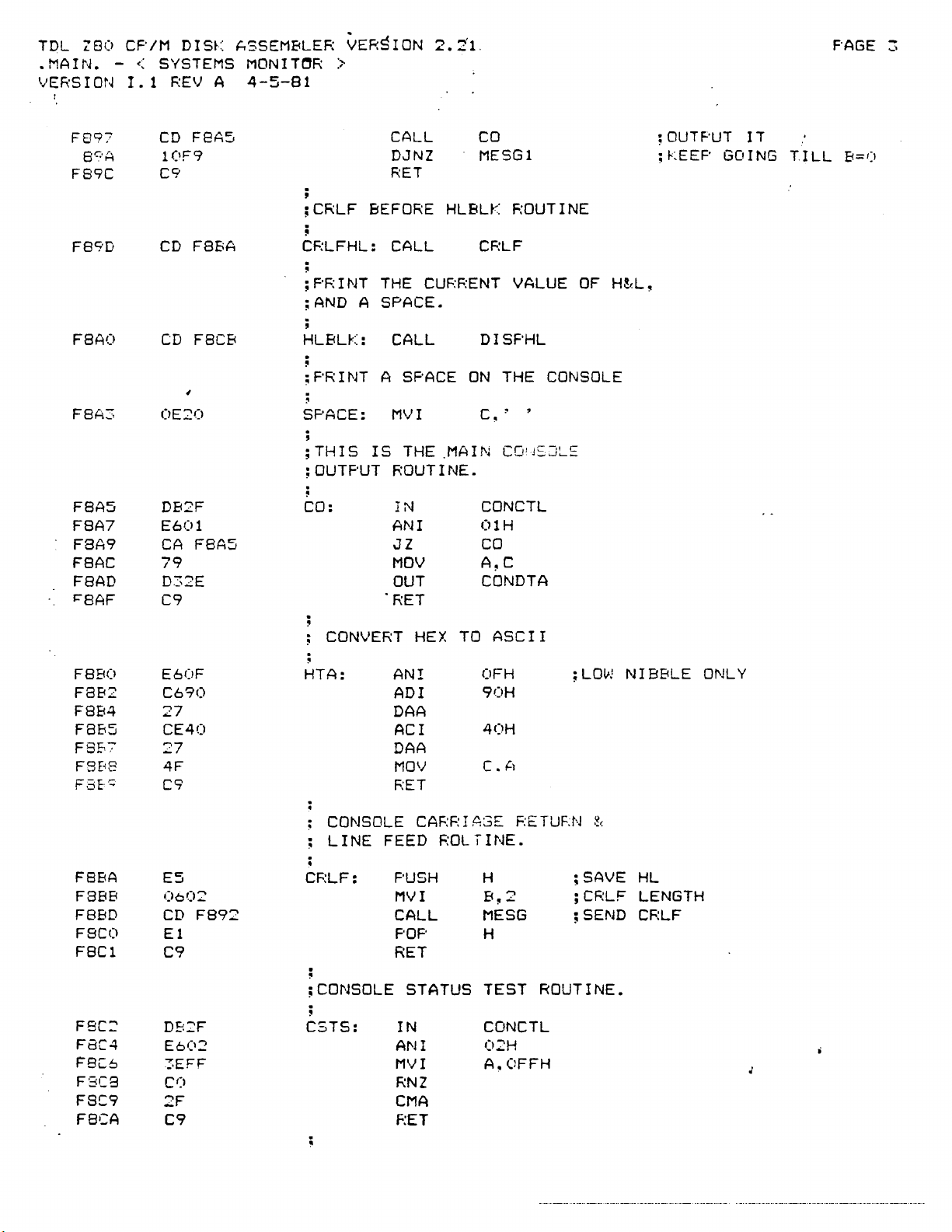
TDL
Z80
CP/M DISK
.MAIN. - < SYSTEMS
VERSION
1.1
REV
A
~SSEM8LER
~ER~ION
MONITOR)
4-5-81
2.t1.
F'AGE 3
CD
F897
F8AS
10F9
F89C
C9
;
;CRLF
F89D
CD
F8BA
CF:LFHL:
;PRINT
;AND A SPACE.
F8AO
CD
F8CB HLBU<:
,
;PRINT
FBA3 OE20 SPACE:
;
;THIS
;
OUTPUT
F8A5
F8A7
F8A9
F8AC
F8AD
~8AF
DB2F
E601
CA
79
D32E
C9
CO:
F8A5
CALL
DJNZ
RET
BEFORE
CALL
THE
CALL
A SPACE
MVI
IS
THE
F:OUT
IN
ANI
JZ
MOV
OUT
"RET
CO
MESGl
HLBLK
CF:LF
CURRENT
DISPHL
ON
C
.MAIN
I NE.
CONCTL
01H
CO
A~C
CONDTA
ROUTINE
VALUE
THE
CONSOLE
~'
,
CC"JS:JL~
OF
;OUTPUT IT
;kEEP
HLL~
GOING
TILL
8=0
F8BO
F8B2
F8B4
F8B5
F8£,7
F8Ei8
F:3E':';
FBBA
F8BB
F8BD
F8Cl)
F8Cl
F8C2
F8C4
F8C6
F8C8
FSC9
F8CA
E60F
C690
27
CE40
27
4F
C9
E5
(l002
CD
E1
C9
DB2F
E6(1~
3EFF
C')
2F
C9
F892
CONVERT
HTA:
AN!
ADI
HEX
TO
ASCII
OFH
90H
;
LOv!
DAA
ACI
DAA
MOV
F:ET
CONSOLE
LINE
CARRIAGE
FEED ROLTINE.
CF:LF: PUSH H
MVI
CALL
POP
RET
;CONSOLE STATUS TEST ROUTINE.
CSTS:
IN
ANI
MVI
RNZ
CMA
F:ET
40H
RETURN
8~2
MESG
H
CONCTL
02H
A.OFFH
~(
;SAVE
;
CF:LF
;SEND
NIBBLE
HL
LENGTH
CF:LF
ONLY
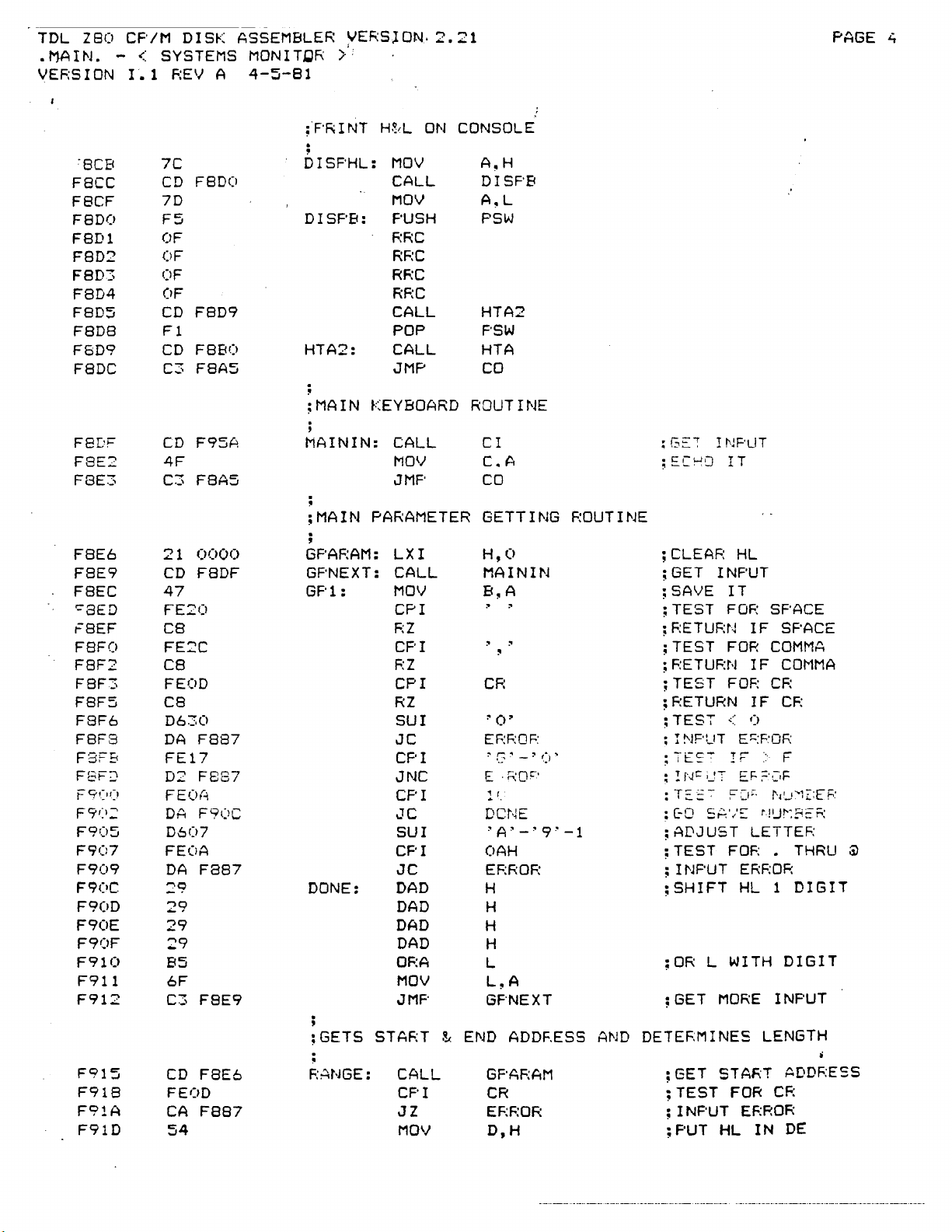
TDl
Z80
.MAIN.
VEF:SION
CP/M
-
1.1
SYSTEMS
<
F:EV
DISK
-
ASSEMBLER
MONIT~R
4-5-81
A
~ERSJON.2.21
>:
PAGE
4
:8CB
Facc
F8CF
F8DCI
F8D1
F8D2
F8D3
F8D4
F8D5
F8D8
F8D9
F8DC
F8Di="
F8E2
F8E3
F8E6
F8E9
F8EC
'='8ED
F8EF
F8FO
F8F2
F8F3
F8F5
F8F6
F8F3
F8FB
F8F:>
F9(")
F9(1:
F905
F907
F909
F9()C
F90D
F90E
F90F
F910
F911
F912
;F'RINT
7C
CD
F8DCl
DISPHL:
70
F5
DISP8:
OF
OF
OF
OF
CD
F8D9
F1
F8BO HTA2: CALL
CD
F8A5
C3
;MAIN
;
CD
4F
C3
F95A
F8A5
MAININ: CALL
;MAIN PARAMETER GETTING ROUTINE
;
21
CD
47
0000
F8DF
GPAF:AM:
GPNEXT:
GF'1
:
FE20
C8
FE2C
C8
FEOD
C8
D630
DA
F887
FE17
D2
F887
FEor-\
DA
F90C
0607
FEOA
DA
F887
29
DONE:
29
29
:9
85
6F
C3
F8E9
;
;GETS
H~rl
ON
CONSOLE
MOV
CALL
MOV
PUSH
F:RC
RF:C
RF:C
RF:C
CALL HTA2
POP
JMP
KEYBOARD
MOV
JMP
LXI
CALL
MOV
CPI
F:Z
CPI
F:Z
CPI
RZ
SUI
JC
CPI
JNC
CPI
JC
SUI
CPI
JC
DAD
DAD
DAD
DAD
OF:A
MOV
JMP
START &
END
A~H
DISF'8
A~L
PSW
PSW
HTA
CO
ROUTINE
C1
C.A
CO
H,O
MAINII'J
B,A
CR
"
0'
EF:F:OF:
E
,RO~'
Dcr·iE
"A'-'9"-1
OAH
EF:ROF:
H
H
H
H
l
l~A
GFNEXT
ADD~E5S
AND
DETERMINES
;G~:
;ECHD
;
;GET
;SAVE
; TEST
;
;TE5T
;
; TEST
;
;
; I
;TE~'!F
;
: T::;;:
: 1:0
;
;TEST
; INPUT
;SHIFT
INPLIT
IT
CLEAF:
HL
INPUT
IT
FOF:
SPACE
F:ETUF:N
F:ETUF:N
F:ETURN
TESi
NF-UT
!f\lc,-,:
FOR
FOF:
,,-
E~:F:OF:
EF-;:'C,F
-;-
FCi"
SA'/::
I F SPACE
COMMA
1F
CF:
1F
t)
r'I'J'CEF:
rJlJ"~?=;:;:
ADJUST LETTEF:
FOR.
ERF:OR
HL
1
;OR l WITH
;GET
MORE
INPUT
LENGTH
CO~lMA
CF:
F
THRU
DIGIT
DIGIT
@
F915
F918
F91A
F91D
CD
FEOD
CA
54
F8E6
F887
F:ANGE:
CALL
CPI
JZ
MOV
GPAF:AM
CR
ERF:OR
D,H
;GET
; TEST
; I
NF'UT
;PUT
STAKT ADDRESS
FOR
CF:
EF:ROR
Hl
IN
DE

TDL
Z80
. MAIN.
VERSION
CP/M
-'(
1.1
DISK ASSEMBLER
SYSTEMS MONIT8R >
REV
A
4-5-81
~ERSION
2.21
..
,
PAGE
5
F91E
'91F
t=9~2
F923
F924
F926
F927
F928
F929
F92A
F92B
F92C
F92F
F931
F934
F935
F93a
F93A
F93D
F940
F941
F944
F945
F947
:94A
5D
CD
E5
B7
ED52
44
4D
62
6B
D1
C9
CD
FEOD
C2
C9
CD
FEOD
CA
22
C5
CD
C1
FEOD
C2
C9
F8E6
F915
F887
F915
Faa7
0023
F8E6
F887
MOV
CALL
PUSH
OF:A
DSBe
MOV
MOV
MOV
MOV
POP
RET
F:ANGE2: CALL
CPI
JNZ
F:ET
F:ANGE3: CALL
CPI
JZ
SHLD
PARAM1: PUSH
CALL
POP
CPI
JNZ
RET
E.L
GPARAM
H )
A
D
B,H
C,L
H,D
L,E
D
F:ANGE
CR
ERF:OF:
F:A!'1GC
CF:
EF:ROR
HLSTR
B
GPAF:AM
B
CF:
ERROF:
;
GET
END
ADDF:,ESS
;SAVE
IT
;END - START'
;PUT
;PUT
;PUT
;GET
; TEST
; INPUT
;GET
;
; INPUT
; SAVE
LENGTH
STAF:T
END
2 PARAMETERS
FOR
EF:ROR
2.
PARA~ETERS
TEST
FOF:
EF:F:OF:
S'"
IN
CF:
CF:
AF:T
;SAVE E
;GET
;
; TEST
; INPUT
3~0
F:ESTOF:E
FOR
PARAMETER
BC
CF:
EF:F:OF:
IN
IN
DE
BC
HL
F94B
F94C
F94D
F94F
F950
F9S1
F~;:
r
~::;5
F956
F959
F95A
F95C
F95E
F961
F963
F965
F~66
F968
F96A
F96D
E5
87
ED52
El
C9
CD
.:
F935
54
5D
2A
(1023
C9
ENDTST: PUSH
OF:A
DSSC
POP
RET
SDL: CALL
MO',/
MOV
LHLD
RET
H
A
D
H
F:~~4;::J:;::
D.H
E.!...
HLSTF:
;SAVE
;HL
; F:ESTORE
HL
-
DE
HL
;RETURN FLAGS
;
SOUF:c.E
;BC
TO
= LENGTH
HL
;MAIN CONSOLE INPUT ROUTINE
DB2F
E602
CA
F95A
DB2E
E67F
C9
DB:~C
E6r)1
C~
F966
79
CI:
;
F'RINTEF:
F'F:INT:
IN
ANI
JZ
IN
ANI
RET
OUTPUT
IN
ANI
JNZ
MOV
CONCTL
02H
CI
CONDTA
7FH
F:OUTINE
INOUT
1
PF:INT
A,C
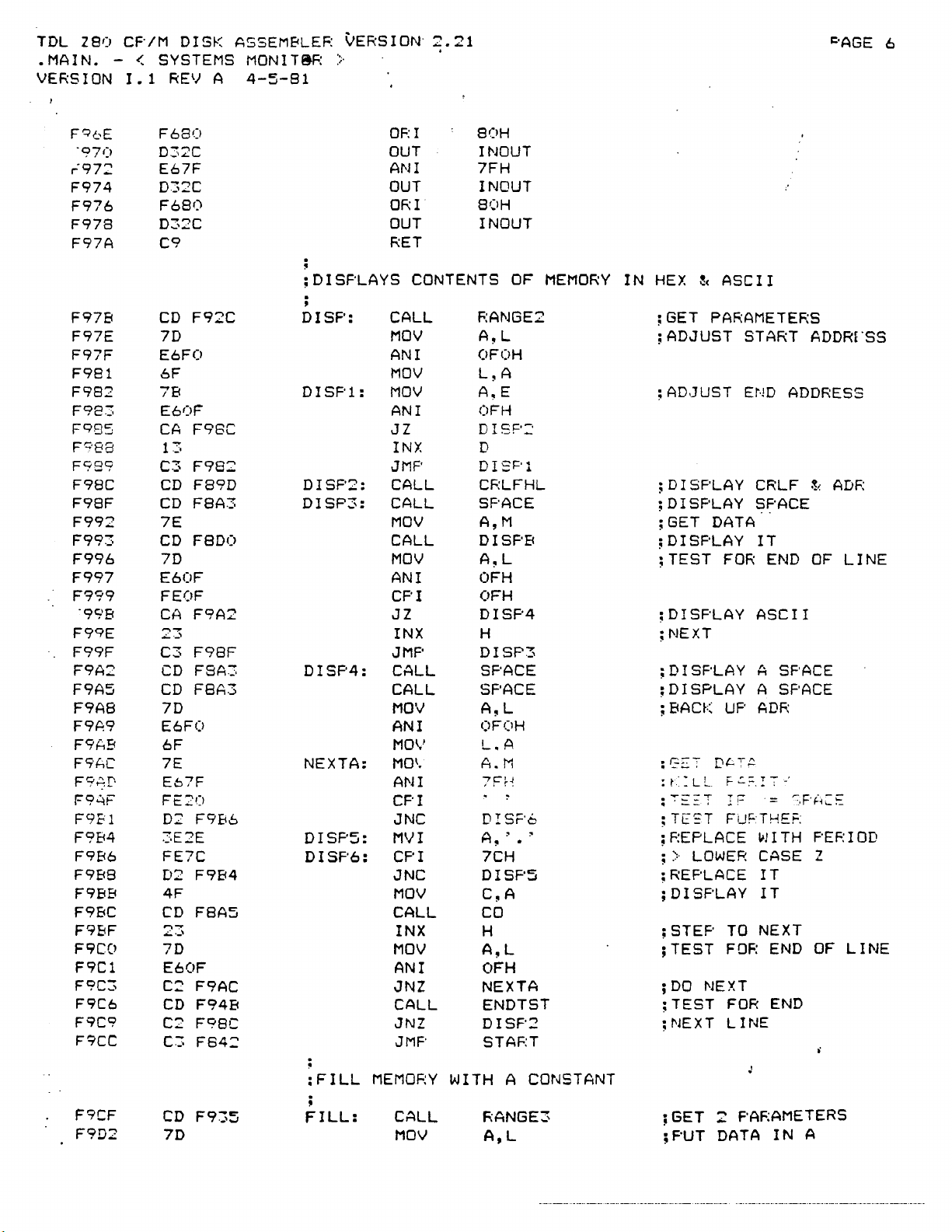
TDL
l80
.MAIN.
VERSION
CP/M
DISK ASSEMBLER
- < SYSTEMS MONIT8F: >
1.1
REV
A
4-5-81
~ERSION'
~.21
I:'AGE
6
FqbE
"97(>
r972
F974
F976
F978
F97A
F978
F97E
F97F
F981
F9S2
F983
F985
q
F
88
F989
F98C
F98F
F992
F993
F996
F997
F999
"998
F99E
F99F
F9A2
F9A5
F680
D32C
E67F
D32C
F680
D32C
C9
CD
7D
E6FO ANI
6F
78
E6
CA
13
C""
CD
CD
7E
CD
7D
E60F
FEOF
CA
'""'
~'-'
C3
CD
CD
F9A8 7D
F9A9
F9AB
FC7'AC
F9.c:.['
F9<4F
F921
F9B4
F986
F988
F9BB
F9BC
F9BF
F9CO
F9C1
F9C3
F9C6
F9C9
F9CC
E6FO ANI
6F
7E
E67F
FE2/)
D2
3E2E
FE7C
D2
4F
CD
'""'
~'-'
7D
E60F
C2
CD
C2
C3
"-'
....
....
F92C
1
)F
F98C
F982
F89D
F8A3
FeDI)
F9A2
F98F
F8A3
FaA3
F9B6
F9B4
F8A5
F9AC
F94B
F98C
F842
;DISPLAYS
;
DISF':
DISP1:
DISP2:
DISP3:
DISP4:
NEXTA:
DISP5:
DISP6:
OF:
I
OUT
ANI
OUT
ORI
OUT
SOH
INOUT
7FH
INOUT
8f~>H
INOUT
RET
CONTENTS OF
CALL
MOV
F:ANGE2
A~L
OFOH
MOV
MOV
ANI
JZ
INX
JMF'
L,A
A,E
OFH
DISF'::
D
DI
S~'
1
CALL CF:LFHL
CALL SPACE
MOV
CALL
MOV
ANI
CPI
JZ
INX
JMP
CALL
CALL
MOV
A,M
DISF'8
A,L
OFH
OFH
DISP4
H
DISP3
SPACE
SPACE
A,L
(lFOH
MOV
MO\.
ANI
CPI
JNC
MVI
CPI
JNC
MOV
CALL
INX
MOV
ANI
JNZ
L.A
A.M
7Ft~
,
DI SF'6
, ,
A,
.
7CH
DISP5
C,A
CO
H
A,L
OFH
NEXTA
CALL ENDTST
JNZ
JMP
DISP2
STAF:T
MEMORY
IN
HEX
&
;
GET
PARAMETEF:S
; ADJUST START
;ADJUST
;DISPLAY
; DISPLAY
;GET
DATA
;DISPLAY
;TEST
;DISPLAY
;NEXT
;DISPLAY
;DISPLAY
;BACK
: t : L L
:~~~-T
;
TE:-ST
;REPLACE
;>
LOWER
;REPLACE
;DISPLAY
;STEP
;TEST
;DO
NEXT
;TEST
;NEXT LINE
ASCII
END
CRLF &
S~'ACE
IT
FOR
END
ASCII
A SPACE
A SPACE
UP
ADR
F-':':=.
r"T.'
IF
=
FUFTHEF:
WITH
CASE Z
IT
IT
TO
NEXT
FOR
END
FOR
END
ADORE
ADDRESS
ADR
OF
LINE
SF'ACE
PERIOD
OF
LINE
"S5
F9CF
F9D2
CD
7D
F935
:FILL
;
FILL:
MEMOF:Y
CALL
MOV
WITH
CONSTANT
A
RANGE3
A,L
;GET
;PUT
=PARAMETERS
DATA
IN
A

TDL
Z80 CPIM DISK
.MAIN. - <
VERSION
1.1
SYSTEMS
REV
A
ASSEMBLER
MONIT~R
4-5-81
VERSION
>
2.21
PAGE
7
F9D3
9['6
F9D7
F9D8
F9D9
F9DA
F9DB
F9DD
F9EO
F9E3
F9E5
F9E8
F9E9
F9EC
FCf~E
F17F
1 FE2C
F9F3
F9F6
F9F9
F9FC
~
~FF
FAOI
l:"A04
:A07
FA09
FAOC
FAOD
FAI0
2A
77
54
5D
13
OB
EDBO
C3
CD
FEOD
CA
4F
CD
FE20
CA
CA
21
CD
,..,.,..,
........
FEOD
CA
CD
FEOD
C2
7E
.....
"'"
._T~
22
FA13 3EFF
FA15
FA16
FA19
FA1;:,
FA1B
FA1F
FA23
FA2?
FA2A
FA2B
FA2E
FA32
FA36
77
2A
E5
F1
ED48
ED58
ED?B
2A
E5
2A
DD2A
FD2A
C9
0023
F842
F95A
FA16
F8A5
FA04
FA04
OCH)(l
F8EC
001E
FA16
F8E6
F887
0020
0021
0010
0012
<)014
0018
00lE
0(116
00lA
00lC
;GOTO
GOTO:
GOT02:
GOTOl
LHLD
MOV
MOV
MOV
INX
DCX
HLSTF:
M,A
D,H
E,L
D
B
LDIR
JMF'
START
USER
PROGRAM
CALL
CPI
JZ
MOV
CALL
CPI
JZ
CPI
JZ
CI
CF:
GOTOI
C,A
CO
.
•
GDT02
,
,
,
GOT02
LXI H,O
GP1
REGSTF:+14
CR
GOTOI
GF'ARAM
CR
ERROR
A,M
OLDOF
BRKSTF:
A,OFFH ;STORE A
M.A
F-:EGSTF.
f-J
F'Sv}
FEGSTF"::
b:EGSTF-'+4
REGSTF:+8
REGSTF:+14
H
REGSTF:+6
:
CALL
SHLD
CPI
JZ
CALL
CPI
JNZ
MOV
STA
SHLD
MVI
f'OV
LHLD
PUSH
POP
LBCD
LDED
LSF'D
LHLD
PUSH
LHLD
LIXD REGSTR+10
LIYD
REGSTF:+12
RET
WITH
OPTIONAL
STAF:T
WRITE
COPY
ADF:
DATA
HL
;DEST =
;ADJUST
;WRITE
DATA
BREAKPOINT
;GET
;TEST
;USE
;ECHO
;T:::ST
:OLD
;TEST
;OLD
;
;GET
;SET
;TEST
;JUMP
;GET
;TEST
; INPUT
;GET
·SAVE
,
;SAVE
:GET
:
;G!:::T
;GET
;GET
;GET
;GET
;GET
;GOTO
INPUT
FOF:
OLD
pr
PC,
CLEAF:
PAF:AMETER
NEW
BF:EAf--F'OINT
OLD
F'Sl;;
>:,-
G~_;-
_l.,
DE
SF'
PC
HL
IX
IY
INPUT
FG=:
FOf=:;
HL,
FOR
TO
FOF:
EF:F:OF:
IT
BF:EA~'::F'O
USER
TO'
HL
AT
START
TO
DE
SOURCE
+ 1
LENGTH
CF:
PC:
VALUE
S!='ACE
NE,·!
BF:f:F'OINT
C:W~~A
NEL'J
ElF:I<POINT
_
PC
CF:
NE\.<J
PC
CF:
OF'
I
NT
BF:EA~:F'O
PROGRAM
ADF:
ADF:
I
NT
FA37
FA3A
'=A3B
FA3C
FA3F
FA40
FA43
CD
19
C5
CD
E1
CD
C3
F92C
F89D
F89D
F84:
;HEXADECIMAL
HEXN:
CALL
DAD
PUSH
CALL
POP H ;GET
CALL
JMP
MATH
F:ANGE2
D
B
CRLFHL
CRLFHL
STAF:T
F:OUTINE
:GET
;ADD
:
;DISPLAY
PAF:AMETERS
PAF:AMETEF:~
SP-,'·.'EDI.FFEF:ENCE
SUM
DIFFEF:ENCE
;DISPLAY
IT

TDL
Z50 CP/M DISK
.MAIN. - <
VERSION
1.1
SYSTEMS
REV
A
ASSEMBLER
MONITQR
4-5-81
VERSION
>
2.21
FAGE
8
FAL
.:,
FA"::?
FAliA
FA4B
FA4D
CD
44
4D
::.EOO
ED47
FA4F ED57
FA51
FA52
FA53
FA54
FA55
FA56
FA57
FP,:;A
FA5E'
FA5C
FA5F
FA60
FA61
FA63
FA64
FA65
FA66
"":',;69
r=AbA
FA6B
FA6C
FA6F
FA70
FA71
FA74
FA75
FA7b
FA'S
FA7A
FA7D
FA7F
FA80
AD
AC
77
23
7C
BA
C2
7D
E<B
C2
60
69
ED57
AD
AC
BE
C4
.....
..,.
...:..~
7C
BA
C2 FA61 JNZ TEST1
7D
BB
C2 FA61 JNZ
60
69
DB2F
E602
C2
ED57
3C
C3
F92C
;EXTEDED
TEST:
MEMOF:Y
CALL
MOV
MOV
MVI
LOOP: STAI
FILL!T:
LDAI
XRA
XRA
MOV
INX
MOV
eMF'
FA4F
JNZ
MOV
CMF'
FA4F JNZ
MOV
MOV
TEST1 : LDAl
XF:A
XF:A
CMP
FA83
CNZ
lNX
MOV
CMF'
MOV
CMP
MOV
MOV
IN
ANI
F842
JNZ
LDAI
INF:
FA4D
JMP
TEST
F:ANGE2
B~H
C~L
A~O
;GET 2
;SAVE
;CLEAR
;BUILD
L
H
M,A
;
l&JF:ITL
H ;NEXT
A.H
;TEST
D
FILlIT
A.L
E
FILLIT
H~B
=
cmnrl'JUE
•
TC'=.T
..
'--
:
COI\JTI>J'_E
;
f.ESTOF:E
L,C
;BUILD
L
H
COMPARE
M
MERR
;
;DISPLAY
H
A,H
;TEST
D
;CONTINUE TEST
A,L
;TEST
E
TESTl
H.P
I :
.....
L.•'_
COi·:C
(l~~;
STAF:7
T~
;CONTINUE
:
F'~SiC"t=E STAr:. T
: TE=.'·:
:
~8GC::7
; I
NCF:EMENT
A
;
LOOF'
ANOTHEF:
F'ARAM.ETEF:S
STAF:T
IN
I
DATA
DATA
DATA
FOF:
END
WF:
ITI
FC'F'
EI'JD
!.'JF:ITING
5THF:T
DATA
IT
EF:RORS
END
FOE
FOR
END
TEST
~.
Er'
E<=~~
c.r·
KE)
IF
TALLY
:::'ASS
Be
NG
FF:ESS~:_
FA63 C5
FA84
FA85
FA88
FA89
FA8C
FASF
FA°(>
FA03
FA94
F5
CD
Fl
CD
CD
7E
CD
Cl
C9
F89D
F8DCl
F8A3
FSDO
MEF:R:
;
MOVE
PUSH
PUSH
CALL
PDF'
CALL
CALL
MOV
CALL
POP
F:ET
BLOCK
OF
MEMORY
B
PSvJ
CF:LFHL
PSL-J
DISF'B
SPACE
A~M
DISF'B
B
;SAVE
;SAVE
BC
DATA
;DISPLAY
;DISPLAY
;DISPLAY
;GET
MEM
;DISPLAY
;
RESTOF:E
;CONTItJUE
ADD~:ESS
DATA
SF'ACE
A
DATA
!T
BC
TESTING

TDL
Z80 CP/M DISK
•MAIN. - <
VERSION
1.1
SYSTEMS
REV
A
ASSEMBLER
MONIT[1t:;:
4-5-B1
..
VERSION
>
2.21
PAGE
9
FA95
~88
t-A9A
CD
C3
FA9D
FAAO
FAA1
FAA3
FAA4
FAA7
FAA8
FAAB
FAAE
FABl
FAB2
FAB4
FAB7
l:"ABA
ABD
FA8E
FAC1
FAC4
FAC7
FAC9
FAce
FA:::
Fr
....
,
t-l_
.:.
FA!:::
FA:'-'5
FAr'7
FADA
FADB
FADE
FADF
FAE2
FAE3
FAE6
FAE9
FAEA
FAEB
FA~C
FAED
-A=:::
FAF')
FAF3 C3
F951
EDBO
F842
F940
CD
4D
ED7S
F5
FBBA
CD
F1
CD
F8DO
F842
C3
CD
F92C
4D
ED59
C3
CD
CD
7E
CD
CD
CD
FEOD
CA
FE20
C2
-.~
~-'
C3
FE7F
C2
2P
C3
4F
CD
E5
:'1
CD
47
7D
El
77
78
FEOD
CA
F842
FBE6
F89D
FSDO
F8A3
F95A
FB42
FAD5
FAB~
FADE
FABA
F8A5
0000
FBEC
FB~2
FAD1
MOVE:
CALL
LDIR
JMP
; INPUT
INPUT:
DATA
CALL
MOV
INP
PUSH
CALL
POP
CALL
JMP
OUTPUT
;
OUTPUT:
DATA
CALL
MOV
OUTP
'::MP
;SUBSTITUTE
SUBS:
SUBSl:
CALL
CALL
MOV
CALL
CALL
CALL
CPI
JZ
CPI
JNZ
SUBS4:
INX
JMP
SUBS2: CPI
JNZ
DCX
JMP
SUBS3:
MOV
CALL
PUSH
LXI
CALL
MOV
MOV
POP
MOV
MOV
CPI
JZ
JMP
FROM
TO
AND
SDL
START
AN
1/0
PARAM1
C~L
A
PSLaJ
CRLF
PSW
DISPB
START
At!
I
/0
RANGE:
C~L
E
STAF:T
EXAMINE
GPAF:AM
CRLFHL
A,M
DISPB
SPACE
CI
CF:
START
5L18S:
=UFS:
7FH
SUBS:::
H
SUBSl
C~A
CO
H
H~O
GPl
B~A
A~L
H
M~A
A~B
CR
STAF:T
SUBS4
PORT
F'0~:T
MEMORY
;SRC~
;
DO
;GET
;
PUT
; INPUT
;SAVE
; DI
;GET
DEST~
MO'v'E
PARAMETER
10
ADF:
DATA
IT
SPLA'Y
CF:LF
DATA
LNGTH
IN C
TO
A
;DISPLAY IT
:GET
; (JUTF'UT
;
;DISPLAY
;GET
~
GET
PAF:AMETEF:
DATA
P~RAMETERS
D~TA
ADDRESS
;DISPLAY IT
SF'LAYASPACE
; DI
;GET
;TEST
INPUT
FOR
CR
;DONE
: TEST
: TEST
:
TL:.~7
; LOm:
F-'h:
SF='ACE
F~'r:;h:::;:';
FC'F-:
F:Ui:':GtJ
FOF
•
,-;~:":"METEF:
;ADDRESS - 1
;CONTINUE DISPLAY
ECHO
;
SAVE
CLEAR
GET
SAVE
PUT
GET
STOF:E
TEST
;
DONE
CHAF:ACTEF:
ADF:
HL
PARAMETER
DELIMITER
DATA
IN
A
ADF:
DATA
FOE
CF-:
;CONTINUE
7
;VERIFY
BLOCK
OF
MEMORY
AGAINST
MEMORY

TDL
Z80 CP/M DISK
.MAIN. - <
VERSION
1.1
AF6
,..·AF9
FAFA
FAFC
FAFF
FBOO
FB03
FB04
FB05
SYSTEMS
REV
A
CD
F951
lA
EDAI
E2
F84:
2B
C4
FA8:;
13
C3 FAF9
ASSEMBLER
MONIT8R
4-5-81
VEF:
VER
;
F:ETURN
VERSION
>
IFY:
1;
CALL
LDAX
eCI
JPO
DCX
CNZ
INX
INX
JMP
FF:OM
2.21
SDL
D
STAF:T
H
MERR
H
D
VERI
BF:EAI<POINTI!EF:E
SF:C.
GET·
DE';T.
DEST
COMPARE
DONE
ADJUST
DI
SPLAY
F:ESTOF:E
DEST
+ 1
CONTINUE
LNGTH
DATA
TO
SOURCE
ADDRESS
EF:F:ORS
ADDRESS
PAGE
10
FB08
FB09
FB(ID
FBll
FB14
FB15
FB18
FB19
FB1A
FB1D
FB20
FB23
FB24
-B28
FB2C
FB30
FB33
FB36
FB:,q
FB3C
FB-:-:E
FB4:;
FB41
FB44
FB47
FB48
FB49
FB4A
FB4B
FB4C
FB4D
FB4E
FB51
FE-=:4
FBS,S
FE-56
FB57
F8'S';
F5
ED43
ED53
22
0012
001
0016
El
E1
2B
22
00lE
2A
0021
3A
0020
77
ED73
DD22 (lOlA
FD22
31
0018
OOlC
OOFF
21 FB5D
0010
11
CD
F8BA
OE08
06(12
C5
CD
F895
CD
F8A3
E5
lA
6F
13
lA
67
13
CD
F8AO
CD
F8A3
El
Cl
OD
CA
F842
C3
FB3E
BF:EA~:::
L
;EXAMINE
XAM:
XAMl
PUSH
SBCD
SDED
SHLD
POF'
SHLD
POP
DCX
SHLD
LHLD
LDA
MOV
SSPD
SIXD
SIYD
LXI
AND
LXI
LXI
CALL
MVI
:
MVI
PUSH
CALL
CALL
PUSH
LDAX
MOV
INX
LDAX
MOV
INX
CALL
CALL
POP
POP
DCR
JZ
JMP
PSvJ
REGSTF:+2
REGSTF+4
F:EGSTE+t
H
REGSTF:
H
H
REGSTR+14
BF:I<STR
OLOOP
M.A
REGSTF:+8
REGSTF:+10
REGSTF:+12
SP,STACK
DISPLAY
H~XAMM
D.
F:EG3TF:
CF:LF
C.8
8.2
B
MESGl
SPACE
H
D
L.A
D
D
H~A
o
HLBL~::
SPACE
H
B
C
START
XAMI
CPU
;SAVE
;
•
;
:
;
;GET
;PC
;STORE
;GET
;
;
;
;
;
REGISTERS
;POINT
;POI~T
: DI S;::'LAy' C
:SET
; SA'/E
;DISPLAI
; DI
;SAVE
;GET REGISTER
;DEST + 1
;DISPLAY
; DI
;GET
;GET
;
;
;CONTINUE
PSW
STOF:E
ST~F:E
STOF:~
GET
STOF:E
BC
DE
Hl_
PSt-)
F'Sl',
PC
- 1
PC
BREAKPOINT
F:ESTORE
STOF:E
SF'
STOF:E
STOF:E
F:ESTOF:E
TO
T;:'i.-.~Y
!::::
SF'LAY
HL
SF'LAY
HL
BC
TALLY.;
DONE
OLD
I X
1'1'
STACk
MES~AGE
TO
REGISTERS
:=;:LF
REG
SPACE
REG
SPACE
1
ADR
OP
NAME
DATA
DATA

TDL
zeo
•
M-AIN.
VERSION
CP/M
- <
1.1
DISI<
SYSTEMS
REV
A
ASSEMB.l..EF:
MONITOF:
4-5-81
VEF:SION
>-
2.2:
PAGE
,:
11
-'85D
,-B5D
FE!6D
FB6F
(lOlA
414642434445
ODOA
53595354454D
XAMM:
.ASCII
MSG:
MSGL
END
;
.END
'AFBCDEHLSPIXIYPC'
MONITOF:
.BYTE
.
ABC
=
OF
PF:OGF:AM
SIGN-ON
CF:,
I I 'SYSTEM
.-MSG
LF
MESSAGE
MONITOR
1.1
REV
A'

·.
•
SBC880
Construction
those
have
who
this
assembling
Be
sure
iron
solder
driver
you
(20
(preferably
and
USE
L
2.
of
have
experience
this
have
W,
100
needle
EYE
PROTECTION WHILE SOLDERING
()
Check
( )
Assembly
the
SBC880
experience
board.
the
proper
degree
63/31),
nose
the
If
anything
report
Install
in
d i
cat
14
pin
in
we
strongly
optimum
pliers.
parts
the
shortage.
the
ed,
sockets
Instructions
from
electronic
tools
diagonal
CAUTION
received
ismissing
following
but
DO
at:
the
bare
suggest
available:
tip
cutters,
NOT
board
assembly.
you
a
temperature),
a
Clat
OR
CUTTING WIRE
against
please
sockets
sol
derthe
in
is
intended
IC
obtain
small
the
contact
the
mat
you
help
soldering
Rosin
blacSe-screw
partslist.
us
locations
t
his
U1-7,U10,U11,U14,U18,U20,U21
do
(or
not
Core
and
tim
in
e.
16
pin
sockets
18
pin
sockets
20pinsocketsat:
24pinsockets
28
pin
socket
40
pin
socket
After
a
sockets
al
and
done
inspect
seated
the
pressing
Now
this
it
all
flat
ternate
9
for
case,
solder
carefUlly
easy
piece
and
of
a 16
each
each
flat
down on
to
of
corner
re-heat
at:
a
the
of
turn
socket
against
the
miss
at:
at:
U17,U26,U29,U30,U31,U32
U24,25
U12,U13,U15,U16,U22,U27,U28,
U33
at:U9,U23
U8
t-
U19
~
-
sockets
cardboard
the
pins
pin
socket.
socket,
to
the
the
the
socket.
remaining
as
the
soldering
have
or
board
of
each
turn
determine
board.
two
pins
density
a
been
styrofoam
over.
SOCket,
After
the
board
that
soldered
of
each
of
the
pin.
inserted
Now
this
If
this
pins
board
After
over
solder
Le.
has
over
it
has
socket.
you
place
pins
been
been
is
while
makes
have
the
1
and
not
Do
1
....
,
•
3.
4.
5.
6.
7.
8.
9.
( )
( )
( )
( )
( )
( )
(
soldered
for
solder
Install
locations
Be
sure
packs
like
that
Install
RP2.
Install
locations
Install
Install
Install
C6,C1.
Install
C8.
Observe
all
the
the
bridges
five
pins,
and
indicatedon
to
install
can
be
soldered
used
and
and
for
solder
solder
Rl,R3,R4,R6,R7,and
and
and
and
and
solder
solder
solder
solder
the
the
the
the
proper
SIP
them
the
the
the
inspect
cold
resistor
the
properly.
to
the
IC
sockets.
lK
DIP
the
six
4.7K
330
ohm
.001
lOOuf
polarity.
each
Joints.
board
(RP1,RP3-RPS).
board
resistor
lK
R8.
resistor
resistor
uf
capacitor
electrolytic
connection
packs
The
by
a
resistors
at
R2.
at
in
the
resistor
method
pack
RS.
at
cap.
at
at
C5,
at
10.
12.
13.
14.
15.
( )
(
( )
( )
( )
Install
C12-C26
)
Install
at
is
Install
Install
I!
you
the
heatsink
pattern
screw
the
the
Carefully,
leads
inserted
"0",
Install
sink
and
and
Cl-C4,C9
observed.
end
the
you
have
use
it.
board
on
with
heatsink,
screw
of
and
"0".
the
is
not
solder
and
solder
5
a good
from
over
the
the
and
using
the
into
required.
solder
Cll.
volt
Insert
the
the
board,
flat
place
tighten
needle
regulator
the
Solder
7812 +12
the
the
1.5ur
Be
sure
the
4MHz
regulator
heat
a
sink
6-32
solder
screw
place
side
a
lockwasher
snugly
solder
the
regUlator
.luf
crystal
machine
and
of
the
nose
such
leads
capacitors
tantalum
the
+
and
and
heatsink
compound,
side,
align
the
regulator
regulator
and
without
pliers,
that
holes
to
labeled
the
at
capacitors
-
at
Yl.
we
screw
place
it
with
i6
forcing.
bend
they
board.
VR2, a
at
CIO,
polarity
at
VR1.
suggest
through
the
the
on
the
against
nut
on
the
can
be
"IN",
heat
16.
17.
( )
)
Install
is
not
Install
the
7905
required.
the
7912
2
-5
-12
regulator
regUlator
at
VR3, a
at
VR4, a
heat
sink
heat

, .
18.
( )
19.
Before
sockets,
caused
the
un-populated
proper
regulators
of
the
to
let
together.
half
the
board
ICts.
All
should
board.
sink
Install
( )
Install
pins
position
top
continuing
inspect
by
solder
supply
can
board
your
If
a
volt
for
integrated
be
is
not
header
and
at
2M/4Mposition.
selects
position
with
the
bridges
board
voltages.
be
measured
(away
from
probes
all
the
or
so),
continue
shorts.
circuits
insertedwith
required.
pins
solder
selects
the
board
or
into
The
on
the
short
voltages
Find
on
pin
the
a
4MHz
a
insertion
carefully
cold
your
output
the
S100
the
are
to
the
short
this
1
toward
at
Jl
and
wire-wrap
The
clock
2MHz
clock.
solder
system
voltages
pin
facing
connector).
voltage
up
to
step
20,
before
board
J2
center
and
of
for
shorts
joints.
and
from
regulator
par
otherwise,
(except
the
and
pins
to
the
center
the
ICs
Now
check
all
toward
Be
careful
(plus
you
install
U1,U2,U3,U4)
bot
tom
solder.
or
header
bottom
in
or
opens
insert
for
the
the
or
minus
check
of..the
"to
the
the
top
not
pins
any
20.
21.
This
( )
InsertthelCsat
assembly
(
Install
option
completes
the
drawing.
whatever
list.
assembly
theindicated
options
of
the
you
SBC880
locations
have
board.
chosen
on
from
the
the
3

PARTS
LIST
Part
Number
CI-4,9,11
CIO,11-26
C5,6,7
C8
Rl,3,4,6-8
R2
R5
RPl,RP3-6
RP2
Ul
U2,
U21
6
16
3
1
6
1
1
5
1
1
2
1.5
uf
.1
uf
Ceramic
.001
lOOuC
uf
Electrolytic
lK ohm,
4.7K
ohm,
330 ohm,
lK
8
pin
lK
ohm
7420
7432
DUAL
QUAD
Tantalum
Ceramic
1/4
watt
1/4
1/4
watt
SIP
Resistor
14
pin
4
IN.
2 IN.
Capacitor
Disc
Disc
Resistor
watt
Resistor
DIP
Resistor
NAND
OR
Capacitor
Capacitor
Capacitor
Resistor
Pack
Pack
GAT"ES
GATES
U3,Ull
U4
US
U6
U7
U8
U9
UIO
U12,
U13
U14
U15
U16
U17
2
1
1
1
1
1
1
1
2
1
1
1
1
7474
7404
7402
DUAL
HEX
NOR
D FLIP
INV.(do
GATE
1489
1488
8251
8253
7400
74LS240
USART
OR
8254
QUAD
OCTAL
TIMER
2 IN.
BUFFERS
7410 TRIPLE 3 IN.
74LS373
74LS374
74112
OCTALDTYPE
OCTALDFLIP
DUAL
J-K
FLIP
FLOP
not
NAND
NAND
use 74LS04)
GATES
GATES
LATCHES
FLOP
FLOP
U18.U20
2
7408
4
QUAD
2 IN.
AND
GATES

U22,
U27
,U28,
U33
4
74LS241
OCTAL
BUFFERS
U23
U24,
U25
U26,U29,U30
U31,U32
VRl
VR2
VR3
VR4
Yl
SW1,SW2,SW3
J1,':"2
1
2
3
2
1
1
1
1
3
2
13
6
2708
2114
8131"OO'1P
74LS367
7805 5
1
7812
7905
7912
4i'.1Hz
Dip
26
14
16
or
RA.'1
12
-5
-12
Crystal
Switch
Pin
pin
pin
2716
ARATORS
or
8097
Volt
Volt
Volt
Volt
6
Header
Sockets
Sockets
EPROM
HEX
Regulator
Reg.(TO
Reg.
Reg.
Position
(TO
(Right
BUFFERS
(TO
220)
220)
(TO
220)
Angle)
220)
18
pin
pin
pin
pin
pin
Screws,
Sockets
Sockets
Sockets
Socket
socket
Pins/Headers
Lockwashers,
&
Nuts
2
8
2
1
1
3
1
2
20
24
28
40
~ire-Wrap
Heatsinks
6-32
5

....
.r
Et7
~
t
co
~
U7
VU
7912
B
v.)
r;;l
t-=J
vn(]~
EJ
EJ
§
HEADER
Jl
r RS232
26
8251
frl
(I5IU~1
UI~:(\6
0
ct
~
.
;rr.
Ii?!t
e4~Q
o ell
~.~'
d
,.bIT"
o?
val
1
~O'"
o
+
(I
L M
J
~
tlO
el2
I I
I(
~
i c==-J i
I 2708
i7i
5
II
14
8253
I
I:
III
, n ,
09
~Q'
~.
0
~
e
17
un
N1
at
100~f
<or
U
I~
....
~
N
....
....
~
AU,.
~R2
UI
1420
~
ula
C::b
ell
~w
un
13
(I
N
....
....
oil-
R7
U1
1432
(I
2M
~o
un
SW'
A6
A7D
AS
A4
A)
aPJ
co
....
W
~
n
R
I
U::~
11
....,
~
r-
~
~
1474
....,
~
r-
tf)
p..)
~
~
U27
P1
21
UJ
(
U19
YI
Z80·A
cs
~
~
~
114
I
....,
~
r-
C/)
p..)
~
rn
u U
~
",~,;.
....,
~
r-
~
~
....
un
3S
co
....
w
....
U2.
.P6[
1404
U4~
~
ij
~
a~1
UlJ
J~l
N a..s
..
0
-IKNY::J
(
.3
~
,Q
en
UJO
HEADER
13
I I/O PORT
26
~
UI4
U10
co
~
....,
(
I
UJI
sac-BBO
so
D
dt>
04
~
U21
'e
un
I
14
J2
I
....,
~
r-
tf)
p..)
~
....
....,
~
r-
~
~
....
UJJ
lIl6
U22
US
;
.-
$
•
,
,.
$

...
---AI
t
----
>5
l
t5
,J
:.:
A7
-'6'
U2'
AS
2.11£
!
I
,..ri"
A3
~
I·~,····
1,.
:'"
r'
I
f2
I
I
~
..--_.
.;:::
..........
+-
-.
-
--
II
iT
II
K:.""~'JI,211
• '
,o;caOO()02
U25
2,IA
OJ
I,
A
1'_
:~117
A6
f-'-'
-+~+-H-+-"
051-"--+--+-+-+-H
AA
I-'--+-+-+-H
A3
",4'--..-J--i-"
"'2
., ,
AI~
A~
Ii--J I
, I
!
--.--
--
---.
;
;
lAM
~
to
U6
II
_
I _
:
, • C14
!!
I I I I I
Il~~
+5
-12
+12
TXCJI.!.!I9~_~
.Q
.~
01
A~
..
"
A2
AI
..,
0'
no
- •
r,s!1
~
n,
n"
wo
Jm
2MHZ
_~~'
.12~
K
I
f
·5
IIP2
IK
•
"i
!n
Z
-I..(j
--
---
2
AI
U21
27~
"ll
VOIl
I
."
-t
--.1
~
~I'~')1~'~2D~~'?_,~ZQ1Jl!!,
I 1
: I : I - C2 I I
~
: • • I
Ii'
I I I I
27/'
."
25/6
"5
....
Al
~1'2
r J
A'
~~~
9,
(j
::
13
14;
T : I
, ,
!
iii
:5:.6
I I
17
, I
I! T
:
"2
i
-/6"'52
...
~
I I
~
~
I
~
n,
..
IN
!
T,"'-
~
~
--r-lL'~
.l.-
CJ I :
i
~~-
"'
11251
I
':-
~,
.5
6 5
f--1
All
+~
W
...
•
....
j
-----,
'"'
____
I
!j<-
:-.;;:'
'-0'
81
S.
7
~
U5
,
1n
..
',-<.,
-,~
.
..;~fl'
:....--~~ch
-_"~=-'-'C~A6
--=---
:'
r.~
- , I
TI
~
j
II
21
r.
-
~
: I
L__....
RP3
U(
~31-
):.".'-------!-J
_5
"'
91
•
SWI
47
~
:....--.~
2~~..
~12'
.15 I
A3
\
r-----+-.----'/Ui4\-12
I!~
(l'.-'~ll
f'
AC
AD
r
",---
.----.
aoZ'
~r----iOI
COl
,35~~274.'5T4Q2'':J
CC,~
:~03
003
;~
D04
~~O!>
[)05
'39~06
006
~07
007
190
~,"~""~
1,
U 6
'6
I
QI
J5
03
04
C4
Q5!
Q6 I 4
Q7 I 7
I
011
Qll
elK
(ll:
II
I U I
.J
,./0
...
I II
,~--
,a:
UI5
'U
01
11~D27434702116
14~03
I
0"
3'05
06
07
De
lin
ql
~
S
QJ.:
Cf4 I,
2
Q5
5
Q6
6
Q7
QIl 9
EN
~
I
I I
i t
__
1==
:~
Of
02
01'
0"
05
Oil
07
(
R
ff~~1]
SE
1;..10'

A7
_ AS
All
-
-
-
-
-
-
-
-
• ..,
,--------
=-=-~--
- ·
,
A9
..
A1
A
A
AI
0
1
!;~
.'
;
"':"
1 1
I i I I I 2
TxC~9~~-----------------------~
ue
&25/
RXG
Tx
-12
+12
19-
~~
n.,
01
n~
WR
lIT>
MHZ
-
.~!~
..~-J.Q
K
1-
511
IK
:i
1'2
t
.!II
O·
~
..
I
22
At
All
'n
A6
AS
A
loA
~
'2
"
9,C':13
U2J
21'~
21'06
27'6
25'6
14.:5;,617
...l.l
..1.
.J AJ
---
~
~--5::~"-~'::2D~:"'C5~2J~
! !
: : . · :
I : • ; \ I I
I I I I
T
iii
I I
I j
, I
"5
+16Vm
-'6'~LW52
I.
II
~
..
(,~
'
liN
16'2.1
VRZ our
Xi'"
-----'
--r------t'N
1.
"'1
vAJ
CJ I
CO'"
1.5.... : + I 1.5
-,.
I
,-
-1------
l
OUTM
!
C'
+ I 1.5oJ
AS
w
c
CIA<:25
.I~r
"'5
T~I:;
~
C'2
CIQ
.,'"
-~
-12
CII
....T.I)Oo.f
..
~IT_J..!K~'4
----j
f:
..
""'.':."':...
~"-~t_-_···~=""-"'C~A6
'0
.,
,52
'9'
~
s.
7
~
---t--..:A'i
">~,.:,
•
~.-~
i/
__
·-.-'--------~.---"~A5
C":'
r:
- I
Ti,.L--,
e
r.
91
I :
I ,14
l
APJ
~2,'.
7 •
SWI:
~'
~----.!---;
•
2~~u
i
21
- "
..
5 CLK
__
~
II(
);'-6
------t-J
~----+
~12'
A7 I I
A,3
.....
·
L
f
DC~
1
I D03
i
I [)(Y5
----
D0'
CC~
004J8~05
006
007
I
~'2
(l'.:~
r'
'.~
AC
AO
PI
§------1,01
';5~,
re:r~03
;~"----:-iD4
.39~.D6
~~07
i90
1
~
r---
-,
U'6
Q'
,;)2'4J'A02:'
'06
.~
Q3,5
Q4
QS,'
Q6
I 4
Q1'
I 7
Q6 I 6
Clt:
II
I
_
~--l
~101,~~~,0'
"102
14
03
I
oA
3'os
D6
0
De
.9 ' I I I I I
02'~6
5
Q3'-'1:oI-
Q4f-'"-------+-+-+-H-----
QS1'2CQ6I-'S'--
1' Q71-'6'--
Qe 9
EN
Clt:
II
I
I
..-
.......
-+-++
-<>-+-++
~-++----
_
_
.....
+ _
~:l?
E.o~~~
--
, sac
:;"
Of
02
OJ'
OA
05
oe
07
:
SCHEMATIC
,..
( T
COMPUTER
PROOUCTS
DIAGRAM
- 2
•

po
"'~
....
~
c
e
'
"'3
.:0.::
3'
.
"&2
=
.E
..
"
"10
~
Aa
Ae
A1
A6
A$
....
A3
A2
A'
~
~
~
~
£
I.!!.
~
:1!.
~
~
L2:
I
•
"
"';'.:,
I"'.
~')2D~8
G~~'
!
I
I
, , .
, t
,
I
I
'~r
'.L~2.'
'6
,01
u2ec;;:]
,21
~'
[7
•
r·
r~
.
,J
~
J;$
0,
..
Al3
A&2
limQ
rnr.
iltTT '
~
1
'
I I
741.t1
I:I~
'L-
~
1.~2.'
U2e<J[..
,
161
'.'52.'
141U2'~
121
~~4~e
I
r
I
-
"V
;,
-1
,
U17
11:.1
~
["
E
19J
r.
re
,-J
r~
I
74~241
r
/1
i"
"-J
lis..
I An
MAIO
3'9'.9
'ili\e
n
~
3~
j4
33
37
3'
,
......
.7
'6
.~
...
'3
&.2
Ai
'-I
•
'A
y
r'..!'~~
U:9
ZBO
iM~~·
meff;
1 I
_
'7
• -
"",:L.:... 5 e 6
"''''
~
"
·rn
I
VA
,.~
~
R3,'"
£~,l
.~
;;c~
~
C$
'~~I
_..-
C6
5
.001
U4
A:4JK
,.404
;:
r
..
===----===-
E===~=====
~
,"
I I
I
~
~
017
016
Ol~
OJ.
013
012
011
Olill
tOO?
{)<yj
OO!}
u04
Ill5IlSI
0D3
002
001
001I
IUlO'f
'AD!'
~j
~.
1,..1'
~
"
><~:
~lJJ
k""
".
I
35
:lEo
..
II,P2
r~
-.L
.~~I~
.U33
~5
t>
1'4LS141
E
74lS~
U33
<]
H6
"
I'
f1
I
~
T •
iOliQ
Fe
~~
0-'050607
ADI"
I I
I I , I
~
1·lu~c!6
"II
lCRQ I I ,
,.
Miil!
WAiT
124
...
·!'
...
,R~
MR
..
~
RP2
,I<
A 8
U
I
~~
o
IA
~
7~
I
FRONT 0
""HAL
~
~
c
RD.IM.
..
!1
l±J
1
~

I
I
I
1'1
.~
C5
.----.
-
~~
MAO
1"._-
~~rc===lC9a
I I
I
!
'_·---11~
Y
-tHt
w-
AC-
~D
1
,
oo~
~.
I
7.(>
'RO~
~~
.
0
C E
.5
.. " .
L/
I-'",Af
.......
""
' I
.....
"
l
 Loading...