

Page 1

Mesh Networking Module
(IEEE 802.15.4)
CTL3212
All information and data contained in this datasheet are subject to change without notice. This publication supersedes and
replaces all information previously supplied. Computime has no responsibility to the consequence of using the information
described in this document.
Copyright © 2016 Computime Limited. All rights reserved.
Rev.2
Page 2

Mesh Networking Module CTL3212
Rev.
Date
(DD-MM-
YYYY)
History
1
11-14-2019
First Released
Revision
Copyright © 2016 Computime Limited. All rights reserved.
Rev. 2
Page 3

Mesh Networking Module CTL3212
Table of Contents
1. General Description ...................................................................................................... 1
2. Applications .................................................................................................................. 1
3. Features ....................................................................................................................... 1
4. Absolute Maximum Ratings .......................................................................................... 2
5. Recommended Operating Conditions .......................................................................... 2
6. Electrical Specifications ................................................................................................ 2
7. Typical application block ............................................................................................... 3
8. Pin Assignment ............................................................................................................ 4
9. Pin Description ............................................................................................................. 4
10. Block Diagram ............................................................................................................ 10
11. RF Frequency Detail................................................................................................... 10
12. PCB Layout Recommendations ................................................................................. 11
13. Antenna test ............................................................................................................... 12
14. Mechanical Dimensions .............................................................................................. 15
15. Regulatory Statements ............................................................................................... 17
Copyright © 2016 Computime Limited. All rights reserved.
Rev.2
Page 4
CTPN
Description
WIPM0RCTL3212-01
MANUA ASSEMBLY CTL3212 ROHS
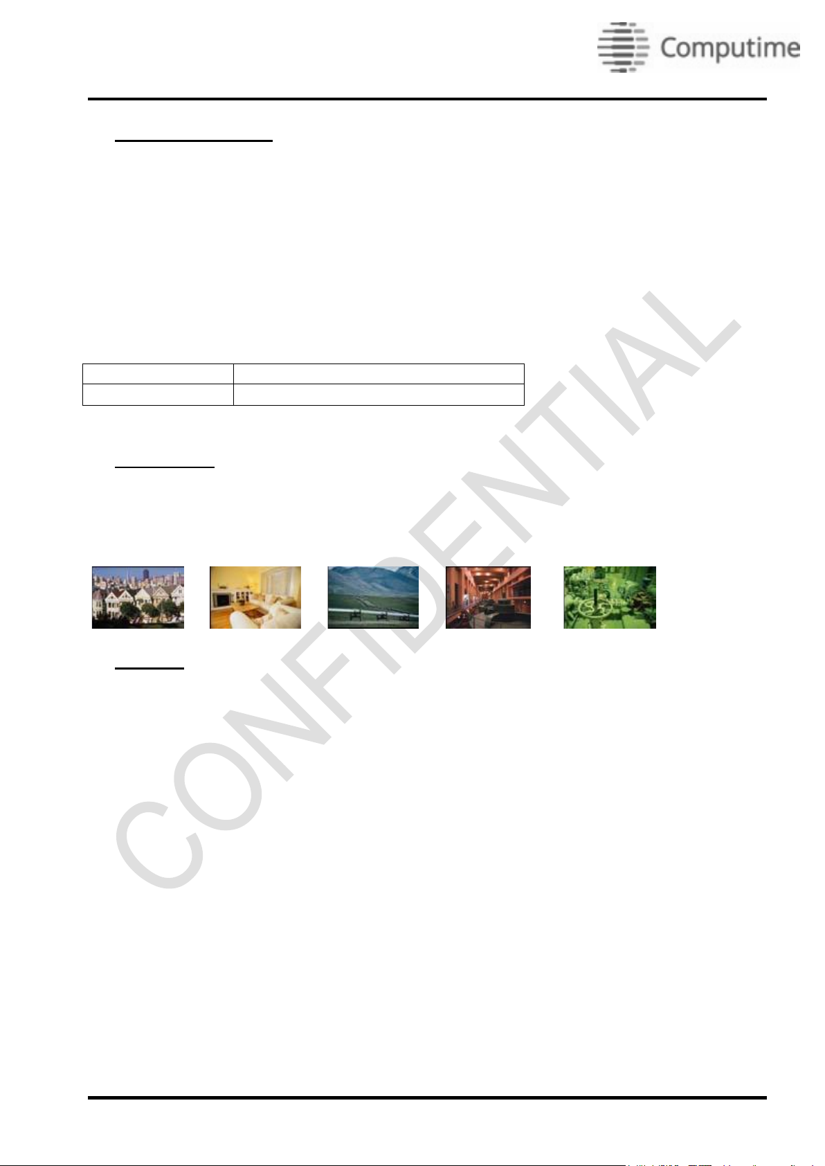
Home
automation &
building control
Home
appliances &
alarms
Monitoring of
remote
systems
Security
systems &
lighting
controls
Sensor data
capture in
embedded
networks
Mesh Networking Module CTL3212
1. General Description
The Module (CTL3212) is a fully-integrated, pre-certified module, enabling rapid development of
wireless mesh networking solutions.
Based on the Silicon Labs EFR32™ Mighty Gecko SoC, the CTL3212 combines an energyefficient, multi-protocol wireless SoC with a proven RF/antenna design and industry leading
wireless software stacks. This integration accelerates time-to-market and saves months of
engineering effort and development costs.
The size of CTL3212 is 22x13x2.6mm.It integrated a 2.4GHz, IEEE 802.15.4-2003 compliant
transceiver with a 32-bit network processor (ARM Cortex-M4 Processor) .It contains embedded
FLASH and integrated RAM for program and data storage.
2. Applications
3. Features
Complete ZigBee-ready module with integrated PCB antenna
Integrated IEEE 802.15.4 PHY and MAC layer
SPI /UART interface for communication and controlled by the Host using the EmberZNet Serial
Protocol (EZSP)
On Board oscillator
High performance direct sequence spread spectrum (DSSS-OQPSK) RF transceiver
16 channels in the 2.4 GHz ISM band
On-chip regulator for 1.8-3.8V operation.
Three deep low power modes
32-bit ARM® Cortex™-M4 processor
512KB FLASH ROM and 64KB RAM(EFR32 internal memory)
+19dBm /+10dBm Max. transmission power
-99 dBm sensitivity (typ)
Small footprint: 22x13x2.6mm
Extremely low Deep Sleep Current.
Copyright © 2016 Computime Limited. All rights reserved.
Rev. 2
Page 5
Mesh Networking Module CTL3212
Parameter
Test Conditions
Min.
Max.
Unit
Voltage on any supply pin
-0.3
+3.8
V
DC voltage on any GPIO pin
-0.3
IOVD
D+0.3
V
Voltage on HFXO pins
-0.3
1.4
V
Storage temperature
-40
+85
°C
Parameter
Test Conditions
Min.
Typ.
Max.
Unit
Regulator input voltage (VDD_PADS)
1.8
3.8
V
Operating temperature range
-10
+55
°C
Moisture Sensitivity Level(MSL)
MSL3
Parameter
Condition / Note
Min
Typ.
Max
Unit
RF Operating frequency
Programmable in 5MHz steps, 5 MHz
steps for IEEE 802.15.4 compliance
2.4 2.5
GHz
Number of channels
For IEEE 802.15.4 compliance
16
Channel spacing
For IEEE 802.15.4 compliance
5
MHz
Frequency stability
+/-40
ppm
Transmit power
Programmable from firmware
+19
dBm
Sensitivity
PER 1% , 250 kbps DSSS-OQPSK
signal
-99 dBm
Adjacent channel rejection +/-5 MHz
IEEE 802.15.4 compliance at -82
dBm
40/40 dB
Adjacent channel rejection +/-10 MHz
IEEE 802.15.4 compliance at -82
dBm
50/50
dB
4. Absolute Maximum Ratings
5. Recommended Operating Conditions
6. Electrical Specifications
T=25℃, VCC = 3.3V, Fo =2450MHz, if nothing else stated.
Copyright © 2016 Computime Limited. All rights reserved.
Rev. 2
Page 6
Mesh Networking Module CTL3212
Parameter
Condition / Note
Min
Typ.
Max
Unit
Supply voltage
1.8 3.8
V
Current consumption,
RX mode
250 kbps, DSSS-OQPSK, 2.4 GHz
12.2
mA
Current consumption, TX mode
200
mA
Deep sleep current
2.8
uA
Flash memory
FLASH memory in EFR32
512
KB
RAM
RAM in EFR32
64
KB
MCU clock frequency
38.4
MHz
MCU Low Speed Clock
External crystal or Internal clock
32.768
KHz
VDD=1.8- 3.8V
Debug and
programming
interface
HOST
MCU
LINK_ACTIVITY
Y1 38.4MHZ
Y2 32.768KHZ
The Y2 is only installed when need an accurate timing reference in low energy modes
ANT 2.4-2.48G
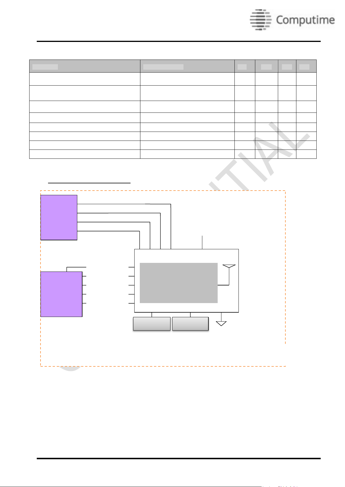
7. Typical application block
NREST
SWCLK
SWDIO
SWO
Note : The Y2 crystal default is not installed (using the internal on chip oscillator)
Figure 1: Example of application circuit
Copyright © 2016 Computime Limited. All rights reserved.
Rev. 2
EFR32MG13
RF Module
Page 7
Mesh Networking Module CTL3212
Module
Pin#
EFR32
Pin#
Pin Alternate Functionality / Description
Analog
Timers
Communication
Radio
Other
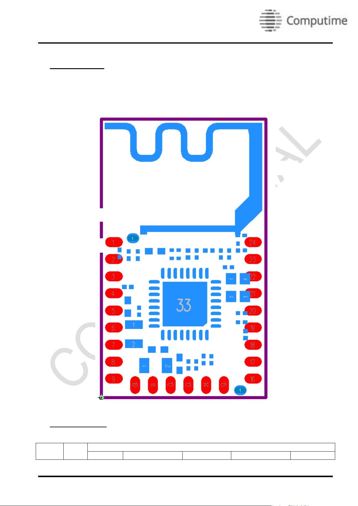
8. Pin Assignment
Figure 2: CTL321X pin assignment
TOP VIEW
9. Pin Description
Copyright © 2016 Computime Limited. All rights reserved.
Rev. 2
Page 8

Mesh Networking Module CTL3212
Module
Pin#
EFR32
Pin#
Pin Alternate Functionality / Description
Analog
Timers
Communication
Radio
Other
1
GND
2
PB11
BUSCY
BUSDX
OPA2_P
TIM0_CC0 #6
TIM0_CC1 #5
TIM0_CC2 #4
TIM0_CDTI0 #3
TIM0_CDTI1 #2
TIM0_CDTI2 #1
TIM1_CC0 #6
TIM1_CC1 #5
TIM1_CC2 #4
TIM1_CC3 #3
WTIM0_CC0 #15
WTIM0_CC1 #13
WTIM0_CC2 #11
WTIM0_CDTI0 #7
WTIM0_CDTI1 #5
WTIM0_CDTI2 #3
LETIM0_OUT0 #6
LETIM0_OUT1 #5
PCNT0_S0IN #6
PCNT0_S1IN #5
US0_TX #6
US0_RX #5
US0_CLK #4
US0_CS #3
US0_CTS #2
US0_RTS #1
US1_TX #6
US1_RX #5
US1_CLK #4
US1_CS #3
US1_CTS #2
US1_RTS #1
LEU0_TX #6
LEU0_RX #5
I2C0_SDA #6
I2C0_SCL #5
FRC_DCLK #6
FRC_DOUT #5
FRC_DFRAME #4
MODEM_DCLK #6
MODEM_DIN #5
MODEM_DOUT #4
MODEM_ANT0 #3
MODEM_ANT1 #2
PRS_CH6 #6
PRS_CH7 #5
PRS_CH8 #4
PRS_CH9 #3
ACMP0_O #6
ACMP1_O #6
3
PB12
BUSDY
BUSCX
OPA2_OU
T
TIM0_CC0 #7
TIM0_CC1 #6
TIM0_CC2 #5
TIM0_CDTI0 #4
TIM0_CDTI1 #3
TIM0_CDTI2 #2
TIM1_CC0 #7
TIM1_CC1 #6
TIM1_CC2 #5
TIM1_CC3 #4
WTIM0_CC0 #16
WTIM0_CC1 #14
WTIM0_CC2 #12
WTIM0_CDTI0 #8
WTIM0_CDTI1 #6
WTIM0_CDTI2 #4
LETIM0_OUT0 #7
LETIM0_OUT1 #6
PCNT0_S0IN #7
PCNT0_S1IN #6#27
US0_TX #7
US0_RX #6
US0_CLK #5
US0_CS #4
US0_CTS #3
US0_RTS #2
US1_TX #7
US1_RX #6
US1_CLK #5
US1_CS #4
US1_CTS #3
US1_RTS #2
LEU0_TX #7
LEU0_RX #6
I2C0_SDA #7
I2C0_SCL #6
FRC_DCLK #7
FRC_DOUT #6
FRC_DFRAME #5
MODEM_DCLK #7
MODEM_DIN #6
MODEM_DOUT #5
MODEM_ANT0 #4
MODEM_ANT1 #3
PRS_CH6 #7
PRS_CH7 #6
PRS_CH8 #5
PRS_CH9 #4
ACMP0_O #7
ACMP1_O #7
4
PB13
BUSCY
BUSDX
OPA2_N
TIM0_CC0 #8
TIM0_CC1 #7
TIM0_CC2 #6
TIM0_CDTI0 #5
TIM0_CDTI1 #4
TIM0_CDTI2 #3
TIM1_CC0 #8
TIM1_CC1 #7
TIM1_CC2 #6
TIM1_CC3 #5
WTIM0_CC0 #17
WTIM0_CC1 #15
WTIM0_CC2 #13
WTIM0_CDTI0 #9
WTIM0_CDTI1 #7
WTIM0_CDTI2 #5
LETIM0_OUT0 #8
LETIM0_OUT1 #7
PCNT0_S0IN #8
PCNT0_S1IN #7
US0_TX #8
US0_RX #7
US0_CLK #6
US0_CS #5
US0_CTS #4
US0_RTS #3
US1_TX #8
US1_RX #7
US1_CLK #6
US1_CS #5
US1_CTS #4
US1_RTS #3
LEU0_TX #8
LEU0_RX #7
I2C0_SDA #8
I2C0_SCL #7
FRC_DCLK #8
FRC_DOUT #7
FRC_DFRAME #6
MODEM_DCLK #8
MODEM_DIN #7
MODEM_DOUT #6
MODEM_ANT0 #5
MODEM_ANT1 #4
CMU_CLKI0 #0
PRS_CH6 #8
PRS_CH7 #7
PRS_CH8 #6
PRS_CH9 #5
ACMP0_O #8
ACMP1_O #8
DBG_SWO #1
GPIO_EM4WU
9
5
PB14
BUSDY
BUSCX
TIM0_CC0 #9
TIM0_CC1 #8
US0_TX #9
US0_RX #8
FRC_DCLK #9
FRC_DOUT #8
CMU_CLK1 #1
PRS_CH6 #9
Copyright © 2016 Computime Limited. All rights reserved.
Rev. 2
Page 9

Mesh Networking Module CTL3212
Module
Pin#
EFR32
Pin#
Pin Alternate Functionality / Description
Analog
Timers
Communication
Radio
Other
LFXTAL_N
TIM0_CC2 #7
TIM0_CDTI0 #6
TIM0_CDTI1 #5
TIM0_CDTI2 #4
TIM1_CC0 #9
TIM1_CC1 #8
TIM1_CC2 #7
TIM1_CC3 #6
WTIM0_CC0 #18
WTIM0_CC1 #16
WTIM0_CC2 #14
WTIM0_CDTI0 #10
WTIM0_CDTI1 #8
WTIM0_CDTI2 #6
LETIM0_OUT0 #9
LETIM0_OUT1 #8
PCNT0_S0IN #9
PCNT0_S1IN #8
US0_CLK #7
US0_CS #6
US0_CTS #5
US0_RTS #4
US1_TX #9
US1_RX #8
US1_CLK #7
US1_CS #6
US1_CTS #5
US1_RTS #4
LEU0_TX #9
LEU0_RX #8
I2C0_SDA #9
I2C0_SCL #8
FRC_DFRAME #7
MODEM_DCLK #9
MODEM_DIN #8
MODEM_DOUT #7
MODEM_ANT0 #6
MODEM_ANT1 #5
PRS_CH7 #8
PRS_CH8 #7
PRS_CH9 #6
ACMP0_O #9
ACMP1_O #9
6
PB15
BUSCY
BUSDX
LFXTAL_P
TIM0_CC0 #10
TIM0_CC1 #9
TIM0_CC2 #8
TIM0_CDTI0 #7
TIM0_CDTI1 #6
TIM0_CDTI2 #5
TIM1_CC0 #10
TIM1_CC1 #9
TIM1_CC2 #8
TIM1_CC3 #7
WTIM0_CC0 #19
WTIM0_CC1 #17
WTIM0_CC2 #15
WTIM0_CDTI0 #11
WTIM0_CDTI1 #9
WTIM0_CDTI2 #7
LETIM0_OUT0 #10
LETIM0_OUT1 #9
PCNT0_S0IN #10
PCNT0_S1IN #9
US0_TX #10
US0_RX #9
US0_CLK #8
US0_CS #7
US0_CTS #6
US0_RTS #5
US1_TX #10
US1_RX #9
US1_CLK #8
US1_CS #7
US1_CTS #6
US1_RTS #5
LEU0_TX #10
LEU0_RX #9
I2C0_SDA #10
I2C0_SCL #9
FRC_DCLK #10
FRC_DOUT #9
FRC_DFRAME #8
MODEM_DCLK #10
MODEM_DIN #9
MODEM_DOUT #8
MODEM_ANT0 #7
MODEM_ANT1 #6
CMU_CLK0 #1
PRS_CH6 #10
PRS_CH7 #9
PRS_CH8 #8
PRS_CH9 #7
ACMP0_O #10
ACMP1_O #10
7
PF1
BUSAY
BUSBX
TIM0_CC0 #25
TIM0_CC1 #24
TIM0_CC2 #23
TIM0_CDTI0 #22
TIM0_CDTI1 #21
TIM0_CDTI2 #20
TIM1_CC0 #25
TIM1_CC1 #24
TIM1_CC2 #23
TIM1_CC3 #22
WTIM0_CDTI1 #31
WTIM0_CDTI2 #29
LETIM0_OUT0 #25
LETIM0_OUT1 #24
PCNT0_S0IN #25
PCNT0_S1IN #24
US0_TX #25
US0_RX #24
US0_CLK #23
US0_CS #22
US0_CTS #21
US0_RTS #20
US1_TX #25
US1_RX #24
US1_CLK #23
US1_CS #22
US1_CTS #21
US1_RTS #20
US2_TX #15
US2_RX #14
US2_CLK #13
US2_CS #12
US2_CTS #11
US2_RTS #10
LEU0_TX #25
LEU0_RX #24
I2C0_SDA #25
I2C0_SCL #24
FRC_DCLK #25
FRC_DOUT #24
FRC_DFRAME #23
MODEM_DCLK #25
MODEM_DIN #24
MODEM_DOUT #23
MODEM_ANT0 #22
MODEM_ANT1 #21
PRS_CH0 #1
PRS_CH1 #0
PRS_CH2 #7
PRS_CH3 #6
ACMP0_O #25
ACMP1_O #25
DBG_SWDIOT
MS
BOOT_RX
8
PF0
BUSBY
BUSAX
TIM0_CC0 #24
TIM0_CC1 #23
TIM0_CC2 #22
TIM0_CDTI0 #21
US0_TX #24
US0_RX #23
US0_CLK #22
US0_CS #21
FRC_DCLK #24
FRC_DOUT #23
FRC_DFRAME #22
MODEM_DCLK #24
PRS_CH0 #0
PRS_CH1 #7
PRS_CH2 #6
PRS_CH3 #5
Copyright © 2016 Computime Limited. All rights reserved.
Rev. 2
Page 10

Mesh Networking Module CTL3212
Module
Pin#
EFR32
Pin#
Pin Alternate Functionality / Description
Analog
Timers
Communication
Radio
Other
TIM0_CDTI1 #20
TIM0_CDTI2 #19
TIM1_CC0 #24
TIM1_CC1 #23
TIM1_CC2 #22
TIM1_CC3 #21
WTIM0_CDTI1 #30
WTIM0_CDTI2 #28
LETIM0_OUT0 #24
LETIM0_OUT1 #23
PCNT0_S0IN #24
PCNT0_S1IN #23
US0_CTS #20
US0_RTS #19
US1_TX #24
US1_RX #23
US1_CLK #22
US1_CS #21
US1_CTS #20
US1_RTS #19
US2_TX #14
US2_RX #13
US2_CLK #12
US2_CS #11
US2_CTS #10
US2_RTS #9
LEU0_TX #24
LEU0_RX #23
I2C0_SDA #24
I2C0_SCL #23
MODEM_DIN #23
MODEM_DOUT #22
MODEM_ANT0 #21
MODEM_ANT1 #20
ACMP0_O #24
ACMP1_O #24
DBG_SWCLKT
CK
BOOT_TX
9
GND
10
PD15
VDAC0_O
UT0ALT /
OPA0_OU
TALT #2
BUSCY
BUSDX
OPA1_N
TIM0_CC0 #23
TIM0_CC1 #22
TIM0_CC2 #21
TIM0_CDTI0 #20
TIM0_CDTI1 #19
TIM0_CDTI2 #18
TIM1_CC0 #23
TIM1_CC1 #22
TIM1_CC2 #21
TIM1_CC3 #20
WTIM0_CDTI0 #31
WTIM0_CDTI1 #29
WTIM0_CDTI2 #27
LETIM0_OUT0 #23
LETIM0_OUT1 #22
PCNT0_S0IN #23
PCNT0_S1IN #22
US0_TX #23
US0_RX #22
US0_CLK #21
US0_CS #20
US0_CTS #19
US0_RTS #18
US1_TX #23
US1_RX #22
US1_CLK #21
US1_CS #20
US1_CTS #19
US1_RTS #18
LEU0_TX #23
LEU0_RX #22
I2C0_SDA #23
I2C0_SCL #22
FRC_DCLK #23
FRC_DOUT #22
FRC_DFRAME #21
MODEM_DCLK #23
MODEM_DIN #22
MODEM_DOUT #21
MODEM_ANT0 #20
MODEM_ANT1 #19
CMU_CLK1 #5
PRS_CH3 #14
PRS_CH4 #6
PRS_CH5 #5
PRS_CH6 #17
ACMP0_O #23
ACMP1_O #23
LES_CH7
DBG_SWO #2
11
PA1
BUSCY
BUSDX
ADC0_EXT
P
VDAC0_EX
T
TIM0_CC0 #1
TIM0_CC1 #0
TIM0_CC2 #31
TIM0_CDTI0 #30
TIM0_CDTI1 #29
TIM0_CDTI2 #28
TIM1_CC0 #1
TIM1_CC1 #0
TIM1_CC2 #31
TIM1_CC3 #30
WTIM0_CC0 #1
LETIM0_OUT0 #1
LETIM0_OUT1 #0
PCNT0_S0IN #1
PCNT0_S1IN #0
US0_TX #1
US0_RX #0
US0_CLK #31
US0_CS #30
US0_CTS #29
US0_RTS #28
US1_TX #1
US1_RX #0
US1_CLK #31
US1_CS #30
US1_CTS #29
US1_RTS #28
LEU0_TX #1
LEU0_RX #0
I2C0_SDA #1
I2C0_SCL #0
FRC_DCLK #1
FRC_DOUT #0
FRC_DFRAME #31
MODEM_DCLK #1
MODEM_DIN #0
MODEM_DOUT #31
MODEM_ANT0 #30
MODEM_ANT1 #29
CMU_CLK0 #0
PRS_CH6 #1
PRS_CH7 #0
PRS_CH8 #10
PRS_CH9 #9
ACMP0_O #1
ACMP1_O #1
LES_CH9
12
PA0
BUSDY
BUSCX
ADC0_EXT
N
TIM0_CC0 #0
TIM0_CC1 #31
TIM0_CC2 #30
TIM0_CDTI0 #29
TIM0_CDTI1 #28
TIM0_CDTI2 #27
TIM1_CC0 #0
TIM1_CC1 #31
TIM1_CC2 #30
TIM1_CC3 #29
WTIM0_CC0 #0
LETIM0_OUT0 #0
US0_TX #0
US0_RX #31
US0_CLK #30
US0_CS #29
US0_CTS #28
US0_RTS #27
US1_TX #0
US1_RX #31
US1_CLK #30
US1_CS #29
US1_CTS #28
US1_RTS #27
FRC_DCLK #0
FRC_DOUT #31
FRC_DFRAME #30
MODEM_DCLK #0
MODEM_DIN #31
MODEM_DOUT #30
MODEM_ANT0 #29
MODEM_ANT1 #28
CMU_CLK1 #0
PRS_CH6 #0
PRS_CH7 #10
PRS_CH8 #9
PRS_CH9 #8
ACMP0_O #0
ACMP1_O #0
LES_CH8
Copyright © 2016 Computime Limited. All rights reserved.
Rev. 2
Page 11

Mesh Networking Module CTL3212
Module
Pin#
EFR32
Pin#
Pin Alternate Functionality / Description
Analog
Timers
Communication
Radio
Other
LETIM0_OUT1 #31
PCNT0_S0IN #0
PCNT0_S1IN #31
LEU0_TX #0
LEU0_RX #31
I2C0_SDA #0
I2C0_SCL #31
13
PF2
BUSBY
BUSAX
TIM0_CC0 #26
TIM0_CC1 #25
TIM0_CC2 #24
TIM0_CDTI0 #23
TIM0_CDTI1 #22
TIM0_CDTI2 #21
TIM1_CC0 #26
TIM1_CC1 #25
TIM1_CC2 #24
TIM1_CC3 #23
WTIM0_CDTI2 #30
LETIM0_OUT0 #26
LETIM0_OUT1 #25
PCNT0_S0IN #26
PCNT0_S1IN #25
US0_TX #26
US0_RX #25
US0_CLK #24
US0_CS #23
US0_CTS #22
US0_RTS #21
US1_TX #26
US1_RX #25
US1_CLK #24
US1_CS #23
US1_CTS #22
US1_RTS #21
LEU0_TX #26
LEU0_RX #25
I2C0_SDA #26
I2C0_SCL #25
FRC_DCLK #26
FRC_DOUT #25
FRC_DFRAME #24
MODEM_DCLK #26
MODEM_DIN #25
MODEM_DOUT #24
MODEM_ANT0 #23
MODEM_ANT1 #22
CMU_CLK0 #6
PRS_CH0 #2
PRS_CH1 #1
PRS_CH2 #0
PRS_CH3 #7
ACMP0_O #26
ACMP1_O #26
DBG_TDO
DBG_SWO #0
GPIO_EM4WU
0
14
PC10
BUSBY
BUSAX
TIM0_CC0 #15
TIM0_CC1 #14
TIM0_CC2 #13
TIM0_CDTI0 #12
TIM0_CDTI1 #11
TIM0_CDTI2 #10
TIM1_CC0 #15
TIM1_CC1 #14
TIM1_CC2 #13
TIM1_CC3 #12
WTIM0_CC0 #30
WTIM0_CC1 #28
WTIM0_CC2 #26
WTIM0_CDTI0 #22
WTIM0_CDTI1 #20
WTIM0_CDTI2 #18
LETIM0_OUT0 #15
LETIM0_OUT1 #14
PCNT0_S0IN #15
PCNT0_S1IN #14
US0_TX #15
US0_RX #14
US0_CLK #13
US0_CS #12
US0_CTS #11
US0_RTS #10
US1_TX #15
US1_RX #14
US1_CLK #13
US1_CS #12
US1_CTS #11
US1_RTS #10
LEU0_TX #15
LEU0_RX #14
I2C0_SDA #15
I2C0_SCL #14
I2C1_SDA #19
I2C1_SCL #18
FRC_DCLK #15
FRC_DOUT #14
FRC_DFRAME #13
MODEM_DCLK #15
MODEM_DIN #14
MODEM_DOUT #13
MODEM_ANT0 #12
MODEM_ANT1 #11
CMU_CLK1 #3
PRS_CH0 #12
PRS_CH9 #15
PRS_CH10 #4
PRS_CH11 #3
ACMP0_O #15
ACMP1_O #15
ETM_TD3
GPIO_EM4WU
12
15
PC11
BUSAY
BUSBX
TIM0_CC0 #16
TIM0_CC1 #15
TIM0_CC2 #14
TIM0_CDTI0 #13
TIM0_CDTI1 #12
TIM0_CDTI2 #11
TIM1_CC0 #16
TIM1_CC1 #15
TIM1_CC2 #14
TIM1_CC3 #13
WTIM0_CC0 #31
WTIM0_CC1 #29
WTIM0_CC2 #27
WTIM0_CDTI0 #23
WTIM0_CDTI1 #21
WTIM0_CDTI2 #19
LETIM0_OUT0 #16
LETIM0_OUT1 #15
PCNT0_S0IN #16
PCNT0_S1IN #15
US0_TX #16
US0_RX #15
US0_CLK #14
US0_CS #13
US0_CTS #12
US0_RTS #11
US1_TX #16
US1_RX #15
US1_CLK #14
US1_CS #13
US1_CTS #12
US1_RTS #11
LEU0_TX #16
LEU0_RX #15
I2C0_SDA #16
I2C0_SCL #15
I2C1_SDA #20
I2C1_SCL #1
FRC_DCLK #16
FRC_DOUT #15
FRC_DFRAME #14
MODEM_DCLK #16
MODEM_DIN #15
MODEM_DOUT #14
MODEM_ANT0 #13
MODEM_ANT1 #12
CMU_CLK0 #3
PRS_CH0 #13
PRS_CH9 #16
PRS_CH10 #5
PRS_CH11 #4
ACMP0_O #16
ACMP1_O #16
DBG_SWO #3
16
GND
17
PF3
BUSAY
BUSBX
TIM0_CC0 #27
TIM0_CC1 #26
TIM0_CC2 #25
US0_TX #27
US0_RX #26
US0_CLK #25
FRC_DCLK #27
FRC_DOUT #26
FRC_DFRAME #25
CMU_CLK1 #6
PRS_CH0 #3
PRS_CH1 #2
Copyright © 2016 Computime Limited. All rights reserved.
Rev. 2
Page 12

Mesh Networking Module CTL3212
Module
Pin#
EFR32
Pin#
Pin Alternate Functionality / Description
Analog
Timers
Communication
Radio
Other
TIM0_CDTI0 #24
TIM0_CDTI1 #23
TIM0_CDTI2 #22
TIM1_CC0 #27
TIM1_CC1 #26
TIM1_CC2 #25
TIM1_CC3 #24
WTIM0_CDTI2 #31
LETIM0_OUT0 #27
LETIM0_OUT1 #26
PCNT0_S0IN #27
PCNT0_S1IN #26
US0_CS #24
US0_CTS #23
US0_RTS #22
US1_TX #27
US1_RX #26
US1_CLK #25
US1_CS #24
US1_CTS #23
US1_RTS #22
US2_TX #16
US2_RX #15
US2_CLK #14
US2_CS #13
US2_CTS #12
US2_RTS #11
LEU0_TX #27
LEU0_RX #26
I2C0_SDA #27
I2C0_SCL #26
MODEM_DCLK #27
MODEM_DIN #26
MODEM_DOUT #25
MODEM_ANT0 #24
MODEM_ANT1 #23
PRS_CH2 #1
PRS_CH3 #0
ACMP0_O #27
ACMP1_O #27
DBG_TDI
18
PD14
BUSCY
BUSDX
VDAC0_O
UT0 /
OPA0_OU
T
TIM0_CC0 #3
TIM0_CC1 #2
TIM0_CC2 #1
TIM0_CDTI0 #0
TIM0_CDTI1 #31
TIM0_CDTI2 #30
TIM1_CC0 #3
TIM1_CC1 #2
TIM1_CC2 #1
TIM1_CC3 #0
WTIM0_CC0 #3
WTIM0_CC1 #1
LETIM0_
OUT0 #3 LETIM0_
OUT1 #2
PCNT0_S0IN #3
PCNT0_S1IN #2
US0_TX #3
US0_RX
#2 US0_CLK #1
US0_CS #0
US0_CTS #31
US0_RTS #30
US1_TX #3
US1_RX
#2 US1_CLK #1
US1_CS #0
US1_CTS #31
US1_RTS #30
LEU0_TX #3
LEU0_RX #2
I2C0_SDA #3
I2C0_SCL #2
FRC_DCLK #3
FRC_DOUT #2
FRC_DFRAME #1
MODEM_DCLK #3
MODEM_DIN #2
MODEM_DOUT #1
MODEM_ANT0 #0
MODEM_ANT1 #31
PRS_CH6 #3
PRS_CH7 #2
PRS_CH8 #1
PRS_CH9 #0
ACMP0_O #3
ACMP1_O #3
LES_CH11
GPIO_EM4WU
8
19
PD13
VDAC0_O
UT0ALT /
OPA0_OU
TALT #1
BUSCY
BUSDX
OPA1_P
TIM0_CC0 #21
TIM0_CC1 #20
TIM0_CC2 #19
TIM0_CDTI0 #18
TIM0_CDTI1 #17
TIM0_CDTI2 #16
TIM1_CC0 #21
TIM1_CC1 #20
TIM1_CC2 #19
TIM1_CC3 #18
WTIM0_CDTI0 #29
WTIM0_CDTI1 #27
WTIM0_CDTI2 #25
LETIM0_OUT0 #21
LETIM0_OUT1 #20
PCNT0_S0IN #21
PCNT0_S1IN #20
US0_TX #21
US0_RX #20
US0_CLK #19
US0_CS #18
US0_CTS #17
US0_RTS #16
US1_TX #21
US1_RX #20
US1_CLK #19
US1_CS #18
US1_CTS #17
US1_RTS #16
LEU0_TX #21
LEU0_RX #20
I2C0_SDA #21
I2C0_SCL #20
FRC_DCLK #21
FRC_DOUT #20
FRC_DFRAME #19
MODEM_DCLK #21
MODEM_DIN #20
MODEM_DOUT #19
MODEM_ANT0 #18
MODEM_ANT1 #17
PRS_CH3 #12
PRS_CH4 #4
PRS_CH5 #3
PRS_CH6 #15
ACMP0_O #21
ACMP1_O #21
LES_CH5
20
VDD
Chip power
input
21
RST
Chip reset
22
GND
23
ANT_E
an optional
external
RF input
24
GND
Copyright © 2016 Computime Limited. All rights reserved.
Rev. 2
Page 13

Mesh Networking Module CTL3212
RF channel
Frequency
11
2405MHz
12
2410MHz
13
2415MHz
14
2420MHz
15
2425MHz
16
2430MHz
17
2435MHz
18
2440MHz
19
2445MHz
20
2450MHz
21
2455MHz
22
2460MHz
23
2465MHz
24
2470MHz
25
2475MHz
26
2480MHz
Application
ZigbeeTM
Network
MAC
RF Transceiver
FEM
32 Bit ARM Processor
38.4M
PCB antenna
DC 1.8V-3.8V
10. Block Diagram
User
UART/SPI/I2C
Communication
IEEE 802.15.4
IEEE 802.15.4
CTL3212
Figure 3: Block Diagram
11. RF Frequency Detail
The following table shows the RF channels as defined by the IEEE 802.15.4 standard.
The use of RF frequencies and maximum allowed RF power should according to different national
regulations. The CTL321X are complying with the applicable regulations for the world wide 2.4GHz
ISM band.
Copyright © 2016 Computime Limited. All rights reserved.
Rev. 2
Page 14

FCC/IC
Channel
CH11~25
CH26
Freq(MHz)
2405~2475
2480
Power setting
19dBm
19dBm ( base on FCC
test result to adjust)
CE
Channel
CH11~CH26
Freq(MHz)
2405~2480
Power setting
10dBm
Mesh Networking Module CTL3212
The following table is the setting for the CTL3212 to US and Europe market:
12. PCB Layout Recommendations
Please reference Mechanical Dimensions shown in next section for PCB layout.
The area underneath the module should be covered with solder mask in order to prevent short
circuit on the test pads on the back side of the module. A solid ground plane under the module is
preferred.
As the module integrated with onboard PCB trace antenna, the mounting position of the module will
have great impact on the RF performance. There should not be any trace, ground plane or metal
part underneath or nearby the area of the onboard PCB trace antenna. The figure below shows an
example how the module positioned on the mother PCB.
Copyright © 2016 Computime Limited. All rights reserved.
Rev. 2
Figure 4: A recommended placement of the module on a main PCB
Page 15
Mesh Networking Module CTL3212
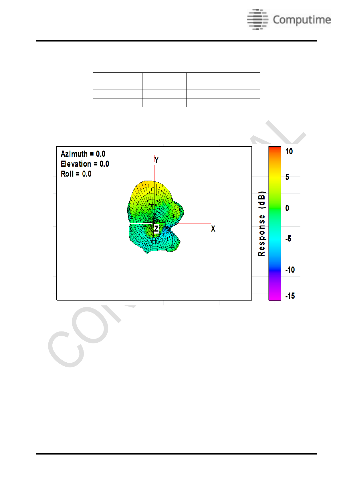
Frequency(MHZ)
Efficidecy (dB)
Efficidecy (%)
Gain(dBi)
2405
-0.75
84.21%
7.28
2440
-0.59
87.26%
7.22
2480
-0.53
88.44%
6.81
13. Antenna test
14.1 Passive OTA test data
14.2 Passive OTA test Pattern
Copyright © 2016 Computime Limited. All rights reserved.
Rev. 2
Page 16

Mesh Networking Module CTL3212
Copyright © 2016 Computime Limited. All rights reserved.
Rev. 2
Page 17
Mesh Networking Module CTL3212
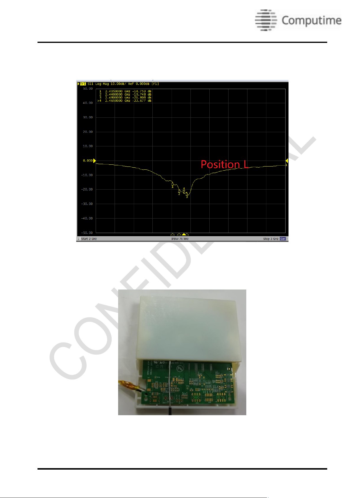
14.3 Antenna S11 Test
14.4 Passive OTA test Unit photo
Copyright © 2016 Computime Limited. All rights reserved.
Rev. 2
Page 18
Mesh Networking Module CTL3212
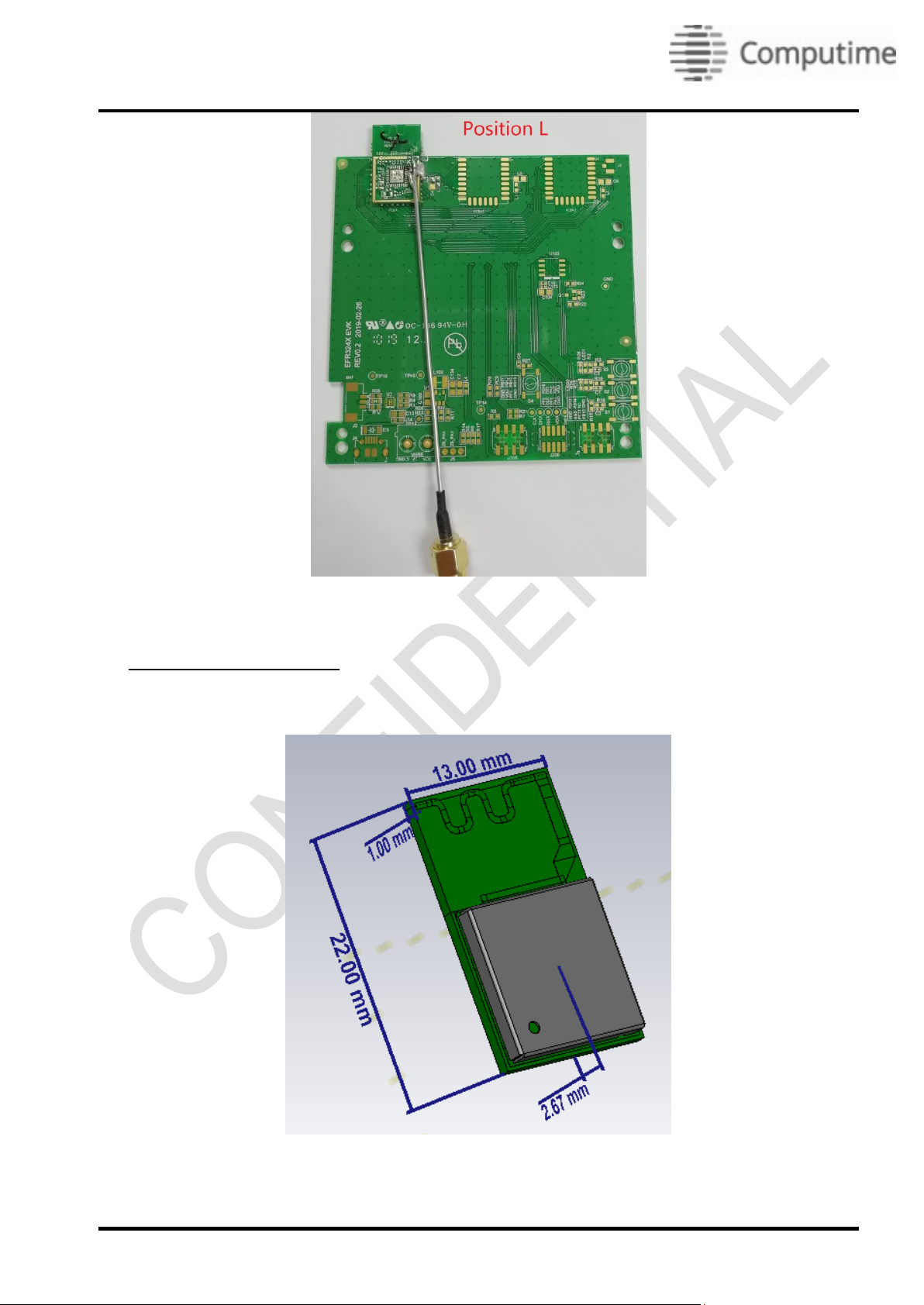
14. Mechanical Dimensions
Figure 5: Mechanical Dimensions of CTL321X
Copyright © 2016 Computime Limited. All rights reserved.
Rev. 2
Page 19

Mesh Networking Module CTL3212
PCB Antenna
For further details on the SoC transceiver (Ember EFR32MG13P)
Copyright © 2016 Computime Limited. All rights reserved.
Rev. 2
Page 20

Mesh Networking Module CTL3212
15. Regulatory Statements
16.1 FCC Statements
This device complies with part 15 of the FCC Rules. Operation is subject to the following two
conditions:
1) This device may not cause harmful interference, and
2) This device must accept any interference received, including interference that may cause
undesired operation.
Cet appareil est conforme à la section 15 des réglementations de la FCC. Le fonctionnement de
l’appareil est sujetaux deux conditions suivantes :
1) cet appareil ne doit pas provoquer d’interférences néfastes, et
2) cet appareil doit tolérer les interférences reçues, y compris celles qui risquent de
provoquer un fonctionnement indésirable.
Note: This product has been tested and found to comply with the limits for a Class B digital device,
pursuant to part 15 of the FCC Rules. These limits are designed to provide reasonable protection
against harmful interference in a residential installation. This product generates, uses, and can
radiate radio frequency energy and, if not installed and used in accordance with the instructions,
may cause harmful interference to radio communications. However, there is no guarantee that
interference will not occur in a particular installation. If this product does cause harmful interference
to radio or television reception, which can be determined by turning the equipment off and on, the
user is encouraged to try to correct the interference by one or more of the following measures:
- Reorient or relocate the receiving antenna.
- Increase the separation between the equipment and receiver.
- Connect the equipment into an outlet on a circuit different from that to which the receiver
is connected.
- Consult the dealer or an experienced radio/TV technician for help.
Warning: Changes or modifications to this unit not expressly approved by the party responsible for
compliance could void the user's authority to operate the equipment.
FCC Radiation Exposure Statement
This equipment complies with FCC radiation exposure limits set forth for an uncontrolled
environment. End users must follow the specific operating instructions for satisfying RF exposure
compliance.
Note 1: This module certified complies with RF exposure requirements under mobile or fixed
condition; this module is to be installed only in mobile or fixed applications.
A mobile device is defined as a transmitting device designed to be used in other than fixed locations
and to generally be used in such a way that a separation distance of at least 20 centimeters is
normally maintained between the transmitter's radiating structure(s) and the body of the user or
nearby persons. Transmitting devices designed to be used by consumers or workers that can be
easily re-located, such as wireless devices associated with a personal computer, are considered to
be mobile devices if they meet the 20 centimeter separation requirement.
Copyright © 2016 Computime Limited. All rights reserved.
Rev. 2
Page 21

Mesh Networking Module CTL3212
A fixed device is defined as a device is physically secured at one location and is not able to be
easily moved to another location.
Note 2: Host product manufacturers must provide in their user manual the required RF exposure
information for mobile & fixed usage of this module. Host product manufacturers must use the
following RF exposure statement in their user manual “This equipment complies with FCC radiation
exposure limits set forth for an uncontrolled environment. This equipment should be installed and
operated with a minimum distance of 20 cm between the radiator and all persons. This transmitter
must not be co-location or operating in conjunction with any other antenna or transmitter.”
Note 3: Any modifications made to the module will void the Grant of Certification, this module is
limited to OEM installation only and must not be sold to end-users, end-user shall have no manual
instructions to remove or install the device, only software or operating procedure shall be placed in
the end-user operating manual of final products.
Note 4: Additional testing and certification may be necessary when multiple modules are used.
Note 5: The module may be operated only with the integral chip antenna with which it is authorized.
Note 6: To ensure compliance with all non-transmitter functions the host manufacturer is
responsible for ensuring compliance with the module(s) installed and fully operational. For example,
if a host was previously authorized as an unintentional radiator under the Supplier’s Declaration of
Conformity procedure without a transmitter certified module and a module is added, the host
manufacturer is responsible for ensuring that the after the module is installed and operational the
host continues to be compliant with the part 15B unintentional radiator requirements. Since this may
depend on the details of how the module is integrated with the host, the manufacturer shall provide
guidance to the host manufacturer for compliance with the part 15B requirements.
Note 7: The FCC ID label on the final system must be labeled with “Contains FCC ID: 2AAUQ-
CTL3212” or
“Contains transmitter module FCC ID: 2AAUQ-CTL3212”.
Note 8: The FCC rule/s for this module are CFR 47 Part 15 Subpart C.
Note 9: This modular transmitter is only FCC authorized for the specific rule parts listed on its grant.
The host product manufacturer is responsible to any other FCC rules that apply to the host not
covered by the modular transmitter grant of certification. The final host product will require Part 15
Subpart B compliance when the modular transmitter is installed.
16.2 ISED Statements`
This device complies with Innovation, Science and Economic Development Canada’s
license-exempt RSS standard(s). Operation is subject to the following two conditions:
1) this device may not cause interference, and
2) this device must accept any interference, including interference that may cause
undesired operation of the device.
Copyright © 2016 Computime Limited. All rights reserved.
Rev. 2
Page 22

Mesh Networking Module CTL3212
Le présent appareil est conforme aux CNR d’Innovation, Sciences et Développement
Èconomique Canada applicables aux appareils radioexempts de licence. L'exploitation est
autorisée aux deux conditions suivantes :
1) l'appareil ne doit pas produire de brouillage, et
2) l'utilisateur de l'appareil doit accepter tout brouillage radioélectrique subi, même si
le brouillage est susceptible d'en compromettre le fonctionnement.
Under Innovation, Science and Economic Development Canada’s regulations, this radio
transmitter may only operate using the integral antenna under which it was approved.
Conformément à la réglementation d’Innovation, Sciences et Développement Èconomique
Canada, le present émetteur radio peut fonctionner avec une antenne fonctionner qu’en
utilisant l’antenne intégrée sous laquelle il a été approuvé.
ISED RF Exposure Statement
This equipment complies with ISED radiation exposure limits set forth for an uncontrolled
environment. This equipment should be installed and operated with minimum distance
20cm between the radiator & your body. This transmitter must not be co-located or
operating in conjunction with any other antenna or transmitter.
Le rayonnement de la classe b repecte ISED fixaient un environnement non
contrôlés.Installation et mise en oeuvre de ce matériel devrait avec échangeur distance
minimale entre 20 cm ton corps.Lanceurs ou ne peuvent pas coexister cette antenne ou
capteurs avec d’autres.
ISED Modular Usage Statement
NOTE 1: When the ISED certification number is not visible when the module is installed
inside another device, then the outside of the device into which the module is installed must
also display a label referring to the enclosed module. This exterior label can use the
wording ”Contains transmitter module IC: 1700A-CTL3212” or “Contains IC: 1700A-CTL3212”.
NOTE 1: Lorsque le numéro de certification ISED n'est pas visible lorsque le module est
installé dans un autre appareil, l'extérieur de l'appareil dans lequel le module est installé
doit également afficher une étiquette faisant référence au module inclus. Cette étiquette
extérieure peut être libellée Contient le module émetteur IC:1700A-CTL3212 ou Contient IC:
1700A-CTL3212.
Copyright © 2016 Computime Limited. All rights reserved.
Rev. 2
Page 23

Mesh Networking Module CTL3212
Contact information
COMPUTIME CORPORATE HQ
9/F Tower One, Lippo Centre,
89 Queensway,
Hong Kong
Tel: +852.2260.0300
Fax: +852.2790.3996
e-mail: hq@computime.com
COMPUTIME NORTH AMERICA HQ,
4700 Duke Dr.
Suite 200
Mason OH 45040
USA
Tel: +1(513).398.2579
Fax: +1(513).754.8955
e-mail: na@computime.com
Cincinnati Technologies
4700 Duke Dr.
Suite 200
Mason OH 45040
USA
Tel: +1(513).754.8935
Fax: +1(513).754.8955
e-mail: ctws@computime.com
About Computime
Founded in 1974, Computime is a global technology, brand and manufacturing company
providing innovative automation and control solutions to customers in commercial, industrial
and consumer markets.
The Company provides technologies and products that save energy and make people's
lives more productive and comfortable.
Copyright © 2016 Computime Limited. All rights reserved.
Rev. 2
 Loading...