

Page 1

SBC-X270
PC/104+ Single Board Computer
Reference Guide
Page 2

Table of Contents
1. REVISION NOTES.................................................................................................... 4
2. INTRODUCTION...................................................................................................... 5
2.1. H
IGHLIGHTS
..........................................................................................................5
2.2. F
EATURES
..............................................................................................................7
2.3. B
LOCK DIAGRAM
................................................................................................ 10
3. CONNECTOR DESCRIPTION.............................................................................. 11
3.1. COM-A C
ONNECTOR ON FRONT PANEL
(P27).................................................... 11
3.2. COM-C H
EADER
(P21)...................................................................................... 11
3.3. USB
HEADER
& LCD
VOLTAGE CONTROL
(P15) ................................................ 12
3.4. A
UDIO
, T
OUCHSCREEN
, W
RITE-PROTECT
(P14).................................................. 12
3.5. RTC, A
UDIO
(P18).............................................................................................. 13
3.6. IDE – H
ARD DISK INTERFACE
(P8, P34)............................................................ 14
3.7. PC C
ARD -
PCMCIA
SLOT
(P6) ......................................................................... 15
3.8. PCMCIA P
OWER HEADER
(E4) .........................................................................16
3.9. C
ARDBUS SLOT
(P7)........................................................................................... 16
3.10. CRT VGA C
ONNECTOR ON FRONT PANEL
(P24)............................................ 18
3.11. LCD P
ANEL CONNECTORS
(P13, P20) ........................................................... 18
3.12. PC/104
CONNECTOR
(P4)................................................................................ 20
3.13. PC/104+ PCI
BUS CONNECTOR
(P5)............................................................... 22
3.14. USB D
UAL CONNECTOR ON FRONT PANEL
(U25)........................................... 24
3.15. M
INI
-USB
TYPE
AB
CONNECTOR
(P36)..........................................................24
3.16. E
THERNET PORT 1 ON FRONT PANEL
(P25)..................................................... 24
3.17. E
THERNET PORT 2 ON FRONT PANEL
(P26)..................................................... 25
3.18. E
THERNET
FPC C
ONNECTOR
(P11)................................................................ 25
3.19. CIF - C
AMERA INTERFACE CONNECTOR
(P22)................................................26
3.20. A
NALOG VIDEO INPUT
(P23)............................................................................27
3.21. GPIO, COM
PORTS AND SPECIAL FUNCTIONS
(P16) ...................................... 28
3.22. JTAG
CONNECTOR
(P19) ................................................................................29
3.23. MMC/SDIO
SOCKET
(P30).............................................................................29
3.24. LPC
CONNECTOR
(P17)................................................................................... 30
3.25. P35 – A/D I
NPUT
............................................................................................. 30
3.26. VGA & COM-A FPC C
ONNECTOR
(P31)......................................................30
3.27. SIM C
ARD SOCKET
(P12)................................................................................ 31
3.28. P
OWER CONNECTORS
...................................................................................... 31
4. FUNCTIONS IMPLEMENTED ON THE SB-X270............................................. 33
4.1. PC/104
AND
IDE
ADDRESSING AND LOGIC
.......................................................... 33
4.2. PC-C
ARD CARDBUS SOCKET
............................................................................... 33
Page 3

SB-X270 PC/104+ Single Board Computer
CompuLab LTD.
3
4.3. 10/100 M
BIT ETHERNET PORT
............................................................................ 34
4.4. RS-232
AND
RS-422/485 S
ERIAL PORT DRIVERS
...............................................34
4.5. LCD P
OWER SWITCH AND
VDD
SELECTION
.......................................................35
4.6. P
OWER SUPPLY OPTIONS
..................................................................................... 36
4.7. CRT I
NTERFACE
- V
IDEO
DAC........................................................................... 37
4.8. F
RONT PANEL
...................................................................................................... 37
5. CONNECTOR LOCATION.................................................................................... 38
6. OPERATING TEMPERATURE RANGES...........................................................41
Page 4
SB-X270 PC/104+ Single Board Computer
CompuLab LTD.
4
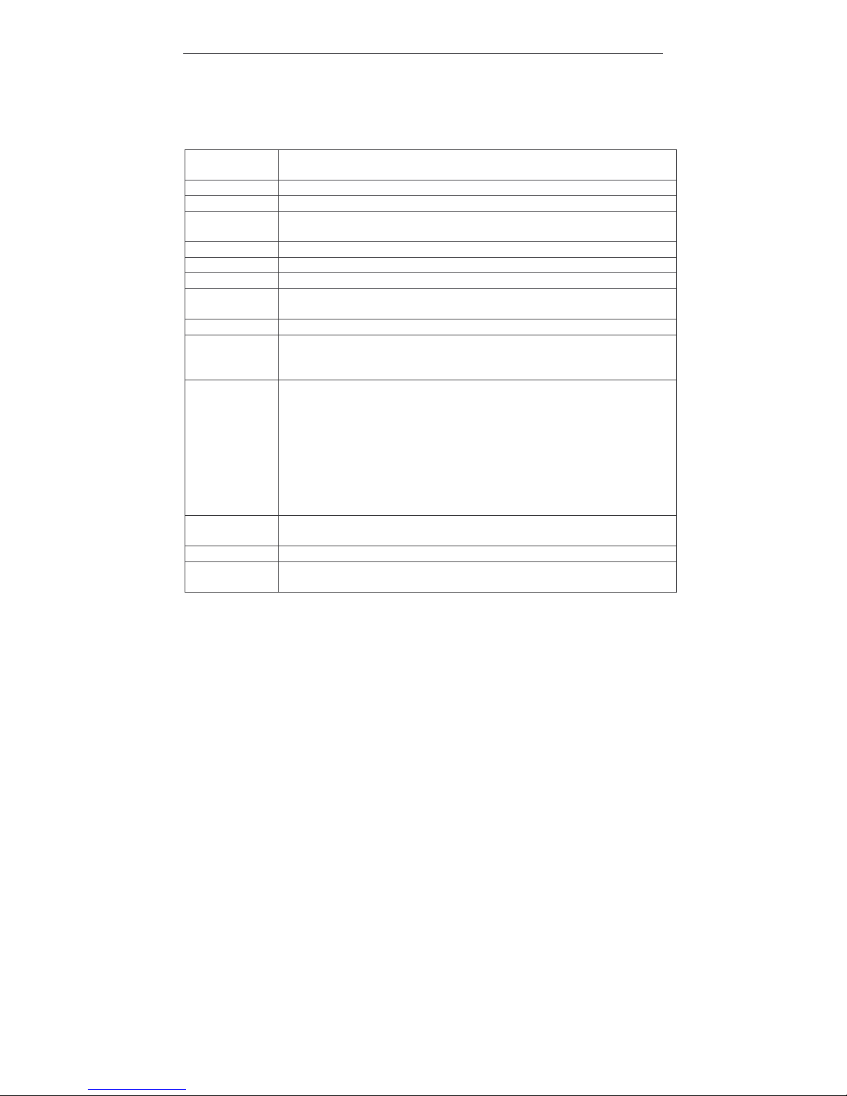
1. Revision Notes
Date
Description
12-May-2006 First release
21-Jun-2006 Updated with WiFi feature
27-Sep-2006 Added E2 jumper description to GPIO section.
Added a note regarding PC-Card voltage constraint to 3.3V only.
04-Dec-2006 Removed irrelevant mentioning of MMC/SD power switch.
21-Dec-2006 Added a note about touchscreen capacitors removal.
4-Jun-2007 Added a comment regarding the availability of PC-104+ slots.
17-Jun-2007 Removed the incorrect comment regarding compatibility with
OV9653 camera module.
02-Jul-2007 Added instructions for front panel removal
10-Sep-2007 GPIO references (P16 connector) were changed to match those of
PXA270.
Added a comment about GPIO usage limitation with CM-X270L
23-Oct-2007 Changes for SB-X270 rev 1.3:
Removed VIP
Added SIM card connector.
Added 40 pos FPC LCD connector.
Added 40 pos FPC IDE connector.
Added A/D connector.
Added mini-USB connector.
Added Bluetooth and GPRS LEDs.
JTAG connector pinout changed.
23-Dec-2007 Removed mentioning of extended graphics controller (2700G, MG
option), as it has been discontinued in CM-X270W module.
31-Mar-2008 Added GPRS voltage modification instructions
13-May-2008 Clarifications made about USB1 and USB4 ports availability on P15
P16-20 changed from GND to VCC3-3
Page 5
SB-X270 PC/104+ Single Board Computer
CompuLab LTD.
5
2. Introduction
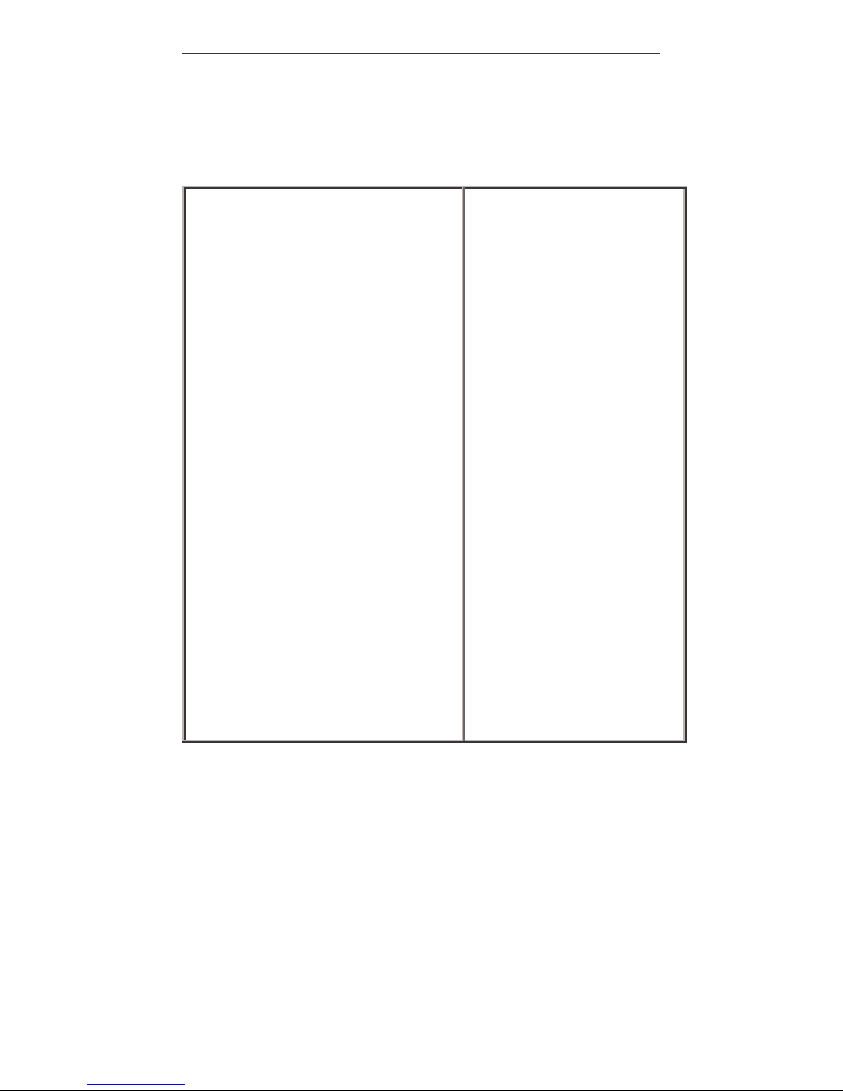
2.1. Highlights
• Single Board Computer implemented by
combination of CM-X270 module and
SB-X270 baseboard. Compatible with
both X270W and X270L module version
• Available in two form-factors:
- Standard PC/104+
- PC/104+ with front panel
• Intel's XScale PXA270 CPU @ 520 MHz,
128 MB SDRAM, 512 MB Flash Disk
• WLAN/WiFi interface
• GPRS/GSM MODEM*
• Bluetooth 2 EDR*
• VGA graphics controller with
connectors for LCD panel and CRT
monitor
• Video input
• PCI and Local Bus expansions in
PC/104+ format
• COM1 - 4 with RS232 / RS485 / RS422 /
TTL driver options
• Host and slave USB ports including
keyboard & mouse support
• Touchscreen interface
• Hard disk interface
• Sound I/O
• Single or dual 100 Mbps Ethernet ports
• PCMCIA, CardBus & MMC/SDIO slots
• RTC with lithium battery
• Switched power supply, 3.3V to 48V
operating range
The SBC-X270 is a standard
PC/104+ compliant, single board
computer. It is implemented by CMX270 module providing most of the
functions, including an integrated
wireless LAN (WiFi) interface,
GPRS/GSM modem and Bluetooth
transmitter. The SB-X270 carrier
board providing connectors and
several additional functions. The rich
features set of the SBC-X270 is
customizable according to the price /
performance targets of the user's
application.
The unique mechanical design of the
SB-X270 allows selecting between
two popular form factors: either a
standard PC/104+ with headers, or an
extended PC/104+ with front panel
connectors.
The SB-X270 contains PC/104+
expansion connectors opening it to
the wide range of standard peripheral
cards. Furthermore, the SB-X270
contains an electrical interface and
slots for PCMCIA, CardBus and
MMC/SDIO extension cards, which
may be inserted and secured in the
slot with no additional mechanical
means, extending the system with
capabilities such as a larger solid state
disk, GPS or GSM modem.
Page 6

SB-X270 PC/104+ Single Board Computer
CompuLab LTD.
6
Notes:
some of above specified features are optional.
* with CM-X270W rev 2 only
Page 7
SB-X270 PC/104+ Single Board Computer
CompuLab LTD.
7
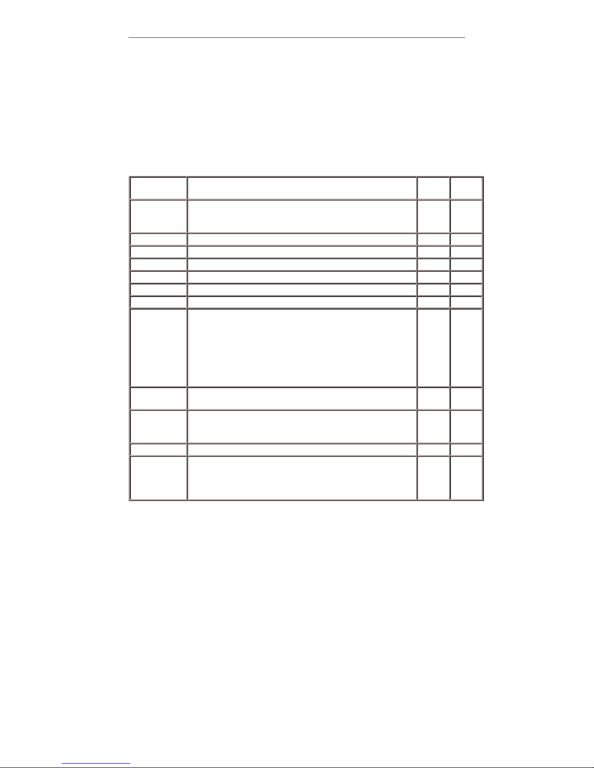
2.2. Features
The "SB Option" column specifies the P/N code of the SB-X270 required for the particular
feature. The "CM Option" column specifies the P/N code of CM-X270 required for the
particular feature. SB-X270 content is the combination of features provided by the attached
CM-X270 and the features implemented on the SB-X270 itself. To have the particular
feature, both the CM and SB options of that feature must be implemented.
"+" means that the feature is always available, regardless of P/N code.
Feature Specification
SB
Option
CM
Option
CPU
SDRAM
Flash Disk
See Features List of CM-X270 module
COM-A Full modem controls, RS-232 levels, RJ11 or DB9 connector + +
COM-B Rx/Tx , RS232 & TTL levels, on 100-mil header + B
COM-C Full modem, RS 232/422/485 levels, standard 10-pin header + +
COM-D Rx/TX, RS-232 & TTL levels, on 100-mil header X +
IrDA SIR and FIR modes. Shared with COM-D + +
IDE PIO mode. Derived from local bus. Standard 40-pin header + +
Ethernet
One or two 10/100BaseT Ethernet ports:
1. Module's port - DM9000, local bus interface
2. Baseboard port Realtek RTL8139 controller PCI interface
RJ-45 connector and activity LED's provided in two options:
- From baseboard's front panel
- Through FPC and optional extension module
+
E2
F1
+
E
E,B
LCD Panel
STN and TFT panel support. 51-pos FPC connector for
direct interface to certain TFT panels
L +
CRT Monitor
RGB signals are derived from the TFT interface using
DAC's.
Interface through DB15 on the front panel or through
FPC and optional module
V +
GPIO 9 to 14 lines, on common 100-mil header. + +
PCMCIA &
CardBus
Slots with card guides, for card types I, II and III. Two
options:
- One slot for PCMCIA / CompactFlash (16-bit) card.
- One PCMCIA slot and one CardBus (32-bit) slot
C1
C2
+
B
Page 8
SB-X270 PC/104+ Single Board Computer
CompuLab LTD.
8
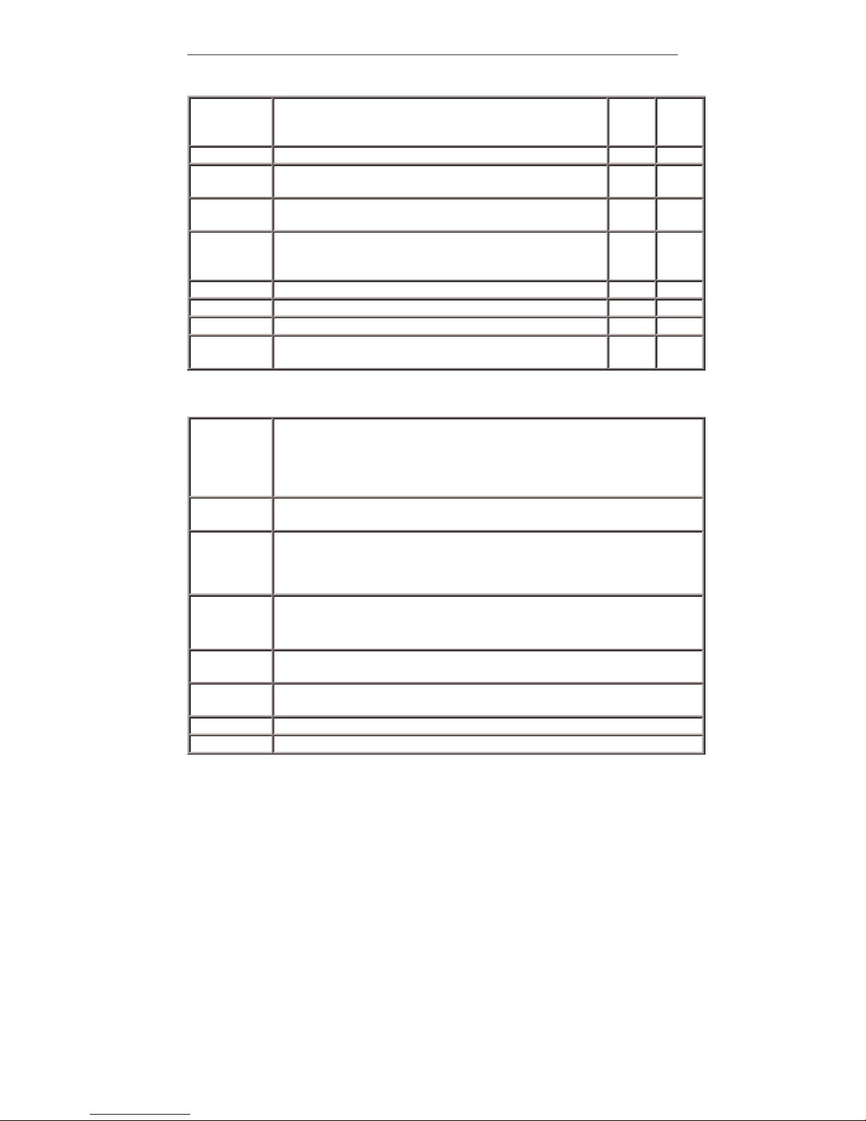
Host USB
Two (default) or four (with "B" option) Host ports, 12 Mbps.
Header for Type-A cable/ connector. Two ports on front
panel.
+ +
Slave USB Slave port shared with USB3 host, 12 Mbps. + +
Touch Panel
UCB1400 controller for resistive panels, pins on 100-mil
header
+ AT
Sound I/O
Header for standard cable/connectors for Microphone
(mono), Line input and Speakers (stereo)
+ A
PC104
Standard PC/104 connector. Signals are derived from the
CPU's local bus through buffers. 20 bit address. No DMA
Support.
P +
PC104+ PCI bus through standard PC/104+ connector R B
RTC Battery Real time clock operated from on-board lithium battery + R
LPC bus LPC bus on common 100-mil header + B
WiFi Interf
WLAN / WiFi including connectors, provided by CMX270L
+ W
Electrical, Mechanical and Environmental Specifications
Supply
Voltage
High efficiency switched power supply. Support of sleep mode.
Three supply options:
- Regulated 3.3V (valid only when the module doesn't contain the "A" option)
- Regulated 5.0V
- Unregulated 12V to 48V
Power
Consumption
2W to 5W in full activity, depending on CPU speed and selected features
Below 50mW in sleep mode
Dimensions
Without front panel - 96 x 91 mm
With front panel - 111 x 91 mm
Height ranges from 10 mm to 22 mm, depending on the connectors assembled.
Height specified includes the CM-X270 module.
Operation
temp (case)
Commercial: 0o to 70o C
Extended: -20o to 70o C
Industrial: -40o to 85o C
Storage
temperature
-40o to 85o C
Relative
humidity
10% to 90% (operation)
05% to 95% (storage)
Shock 50G / 20 ms
Vibration 20G / 0 - 600 Hz
Page 9

SB-X270 PC/104+ Single Board Computer
CompuLab LTD.
9
MTBF > 100,000 hours
Page 10
SB-X270 PC/104+ Single Board Computer
CompuLab LTD.
10
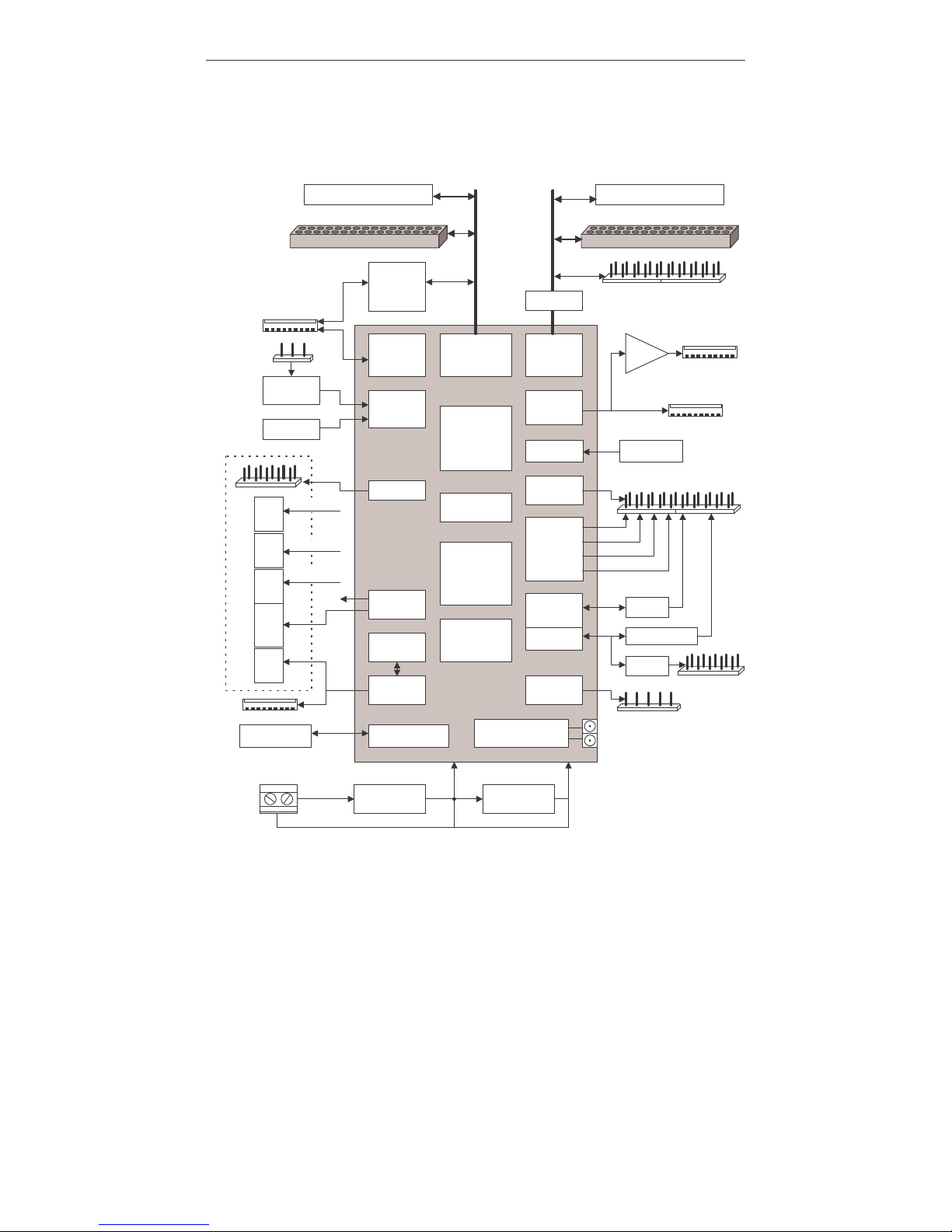
2.3. Block Diagram
Front Panel (option F)
CM-X270
COM-A
100Mb
Ethernet
Graphics
Controller
4x USB
Audio
codec
PCI
Bridge
CPU
RS232
SDRAM
Flash Disk
ARMmon
RTC
PCMCIA slot (opt C1)CardBus slot (opt C2)
PC/104+ (PCI) (option R)
Battery
100Mb
Ethernet
(opt E2)
PC/104 (ISA) (option P)
1.9
FPC, 51-pos
FPC
RJ45 DB15RJ45RJ11 USBx2
RS232
RS422/485
FPC, 20-pos
Touchscreen
VGA
ETHR1
ETHR2
DAC
CIF conn.
Video
Encoder
JTAG
Local Bus
&
PCMCIA
Buffers
FPC &
to front panel
COM-B
COM-D
COM-C
RS232
MMC/SDIOSocket
Camera
Interface
GPIO
LPC
I2C/SSP
USIM
Step-down
converter
Step-down
converter
5V
Power Entry
12-48V
3.3V
Analog
Video In
Hard Disk Header
WiFi Interface
Antenna connectors
Page 11
SB-X270 PC/104+ Single Board Computer
CompuLab LTD.
11
3. Connector Description
The SB-X270 uses the attached CM-X270 module to implement most of the provided
functions. For these functions, the SB-X270 routes the signals from the CM-X270’s
miniature connectors to the standard connectors. The function’s description is therefore
provided in the CM-X270 Reference Guide. The section below provides only the
description of the external interface connectors. The subsequent section provides the
specifications of those functions implemented on the SB-X270 itself.
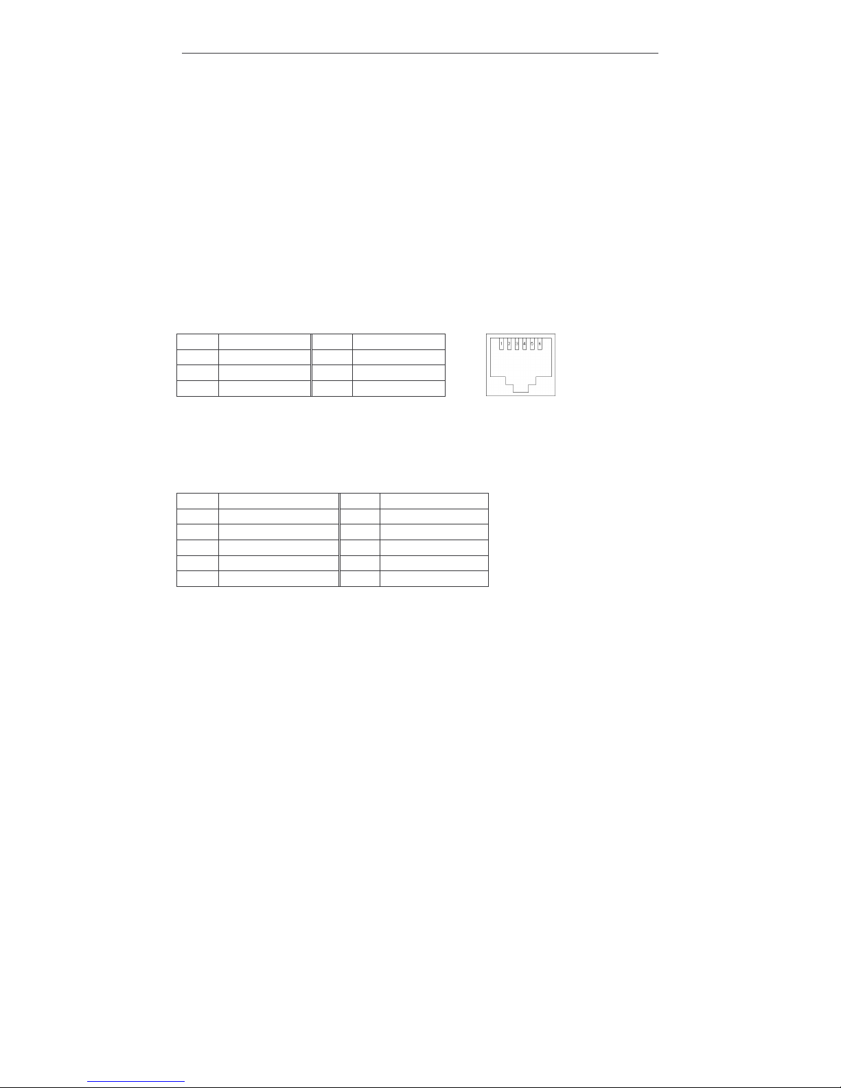
3.1. COM-A Connector on Front Panel (P27)
RJ-11 6-pin connector, compatible with a standard RJ11 / DB9 cable (available from
CompuLab). RS-232 level Rx/Tx/RTS/CTS are provided, other modem control lines are
not available. This connector is available only with the front panel option.
Pin Name Pin Name
1 COM-A-RTS# 2 GND
3 COM-A-TX 4 COM-A-RX
5 GND 6 COM-A-CTS#
3.2. COM-C Header (P21)
2x5, 100 mil header, compatible with a standard DB9 cable/connector. RS-232 or TTL
levels, depending on assembled option. Includes modem control lines.
Pin Name Pin Name
1 COM-C-DCD# 2 COM-C-RX
3 COM-C-TX 4 COM-C-DTR#
5 GND 6 COM-C-DSR#
7 COM-C-RTS# 8 COM-C-CTS#
9 COM-C-RI# 10 -
COM-C is also routed to the P16 header (see below) for interfacing RS485/422.
Page 12
SB-X270 PC/104+ Single Board Computer
CompuLab LTD.
12
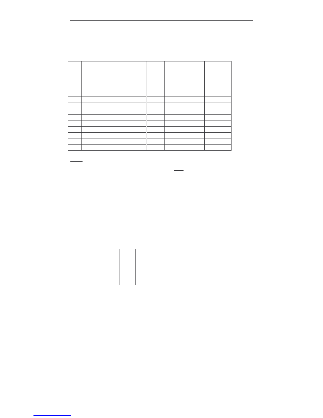
3.3. USB header & LCD voltage control (P15)
1x26, 100 mil header. USB pin assignment is directly compatible with standard
cables/connectors.
Pin Name
Wire
Color
Pin Name Wire
Color
01 VCC3.3 14 USB3-P Green
02 VSRC-LCD 15 GND Black
03 VCC5 16 SHIELD
04 GND 17 VCC-USB2 Red
05 VCC-USB1 Red 18 USB2-N White
06 USB1-N White 19 USB2-P Green
07 USB1-P Green 20 GND Black
08 GND Black 21 SHIELD
09 SHIELD 22 VCC-USB4 Red
10 VCC-USB3 23 USB4-N White
11 VCC-USB3-BUS 24 USB4-P Green
12 VCC-USB3-BUS Red 25 GND Black
13 USB3-N White 26 SHIELD
Notes
• An LCD power supply voltage selection jumper must be assembled in either 1-2 or 2-3
position for normal LCD functionality.
• A jumper must be assembled on pins 10-11 to provide power, if USB3 is used in host
mode. A jumper must be removed when USB3 is used in slave mode. Jumper only
selects power; the switching between host and slave modes is controlled by ARMmon
command.
• If card includes “F” (front panel) option, then USB1 is routed to the front panel rather
than to P15 header. To change this assignment, user must remove RN40 bypass and
solder it in RN38 location. In cards without “F” option, this is a default assignment.
• USB4 port is available only with CM-X270W module.
3.4. Audio, Touchscreen, Write-protect (P14)
P14 - 1x18 100 mil header
Pin Name Pin Name
1 TSMX 10 GND
2 TSMY 11 GND
3 TSPY 12 LOUT-L
4 TSPX 13 LIN-R
5 NAND-WP#* 14 GND
Page 13
SB-X270 PC/104+ Single Board Computer
CompuLab LTD.
13
6 GND 15 GND
7 NOR-WP#* 16 LIN-L-MIC*
8 GND 17 VCC5
9 LOUT-R 18 GND
Notes
• Pull pins 5 & 7 low to write protect CoM’s NAND and NOR flashes respectively. For
this purpose jumpers can be assembled on P14 5-6 and/or P14 7-8.
• MIC-IN and IN-L signals are connected together; consequently, microphone recording
and line recording can’t be done simultaneously.
• In early versions of SB-X270 there are 4 capacitors assembled, which sometimes
affect touchscreen operation. If you are facing touchscreen problems, please remove
C140, C143, C150, C151. For capacitors location refer to [Developer] >> [X270] >>
[SB-X270 Design] links in CompuLab's web-site.
3.5. RTC, Audio (P18)
1x3 100 mil header
Pin Name
1 GND
2 VBAT
3 SPDIF
Page 14
SB-X270 PC/104+ Single Board Computer
CompuLab LTD.
14
3.6. IDE – Hard Disk Interface (P8, P34)
P8 - Standard 40-pin header, directly compatible with an IDE flat cable
Pin IDE signal CM-X270
connector
pin name
Pin IDE signal CM-X270
connector
pin name
1 RESET# RST-OUT# 2 GND GND
3 DATA7 LB-D7 4 DATA8 LB-D8
5 DATA6 LB-D6 6 DATA9 LB-D9
7 DATA5 LB-D5 8 DATA10 LB-D10
9 DATA4 LB-D4 10 DATA11 LB-D11
11 DATA3 LB-D3 12 DATA12 LB-D12
13 DATA2 LB-D2 14 DATA13 LB-D13
15 DATA1 LB-D1 16 DATA14 LB-D14
17 DATA0 LB-D1 18 DATA15 LB-D15
19 GND GND 20 KEY 21 DMAREQ - 22 GND GND
23 IOW# LB-IDE-WR# 24 GND GND
25 IOR# LB-IDE-RD# 26 GND GND
27 IOCHRDY LB-IORDY 28 CSEL GND
29 DMAACK# - 30 GND GND
31 IRQ IDE-INT 32 IOCS16# 33 ADDR1 LB-A4 34 PDIAG 35 ADDR0 LB-A3 36 ADDR2 LB-A5
37 CS0# IDE-CS0# 38 CS1# IDE-CS1#
39 DASP# (Pullup, LED) 40 GND GND
* Signals marked in gray are not supported.
P34 - 40-pin FPC connector, for IDE interface module available from CompuLab.
Pin IDE signal Pin IDE signal
1 DATA8 21 DATA2
2 VCC5 22 DATA1
3 DATA9 23 GND
4 DATA10 24 DATA0
5 VCC5 25 CS0#
6 DATA11 26 GND
7 DATA12 27 IOCHRDY
8 GND 28 IRQ
Page 15
SB-X270 PC/104+ Single Board Computer
CompuLab LTD.
15
9 DATA13 29 IOW#
10 DATA14 30 GND
11 GND 31 ADDR0
12 DATA15 32 IOR#
13 DATA7 33 GND
14 GND 34 CS1#
15 DATA6 35 DMAACK#
16 DATA5 36 ADDR2
17 GND 37 GND
18 DATA4 38 ADDR1
19 DATA3 39 DMAREQ
20 GND 40 RESET#
3.7. PC Card - PCMCIA slot (P6)
The 68-pin PC Card slot conforms to the PCMCIA standard. It includes card guides.
Pin PCMCIA
Signal
CM-X270
connector
pin name
Pin PCMCIA
Signal
CM-X270
connector
pin name
1 GND GND 35 GND GND
2 D3 LB-D3 36 CD1# PCM-CDA#
3 D4 LB-D4 37 D11 LB-D11
4 D5 LB-D5 38 D12 LB-D12
5 D6 LB-D6 39 D13 LB-D13
6 D7 LB-D7 40 D14 LB-D14
7 CE1# PCM-CE1# 41 D15 LB-D15
8 A10 LB-A10 42 CE2# PCM-CE2#
9 OE# PCM-MEMR# 43 VS1# 10 A11 LB-A11 44 IOR# PCM-IOR#
11 A9 LB-A9 45 IOW# PCM-IOW#
12 A8 LB-A8 46 A17 LB-A17
13 A13 LB-A13 47 A18 LB-A18
14 A14 LB-A14 48 A19 LB-A19
15 WE# PCM-MEMW# 49 A20 LB-A20
16 RDY#
IREQ#
PCM-IRQ1 50 A21 LB-A21
17 VCC VCC-P1* 51 VCC VCC-P1*
18 VPP1 5V 52 VPP2 5V
19 A16 LB-A16 53 A22 LB-A22
Page 16
SB-X270 PC/104+ Single Board Computer
CompuLab LTD.
16
20 A15 LB-A15 54 A23 LB-A23
21 A12 LB-A12 55 A24 LB-A24
22 A7 LB-A7 56 A25 LB-A25
23 A6 LB-A6 57 VS2# 24 A5 LB-A5 58 RESET PCM-RST
25 A4 LB-A4 59 WAIT PCM-WAIT#
26 A3 LB-A3 60 INPACK# N/C
27 A2 LB-A2 61 REG# PCM-REG#
28 A1 LB-A1 62 BVD2/SPK 29 A0 LB-A0 63 BVD1/STS 30 D0 LB-D0 64 D8 LB-D8
31 D1 LB-D1 65 D9 LB-D9
32 D2 LB-D2 66 D10 LB-D10
33 WP/IOIS# PCM-IOS16# 67 CD2# 34 GND GND 68 GND GND
* See section 3.8
3.8. PCMCIA Power Header (E4)
This header selects the VCC voltage for PCMCIA / CompactFlash cards in the PCMCIA
slot. The SB-X270 does not support automatic voltage selection, so the user is responsible
for setting the correct VCC voltage before inserting the card, by shorting the appropriate
pins on E4. For 5V supply, short pins 1-2 and for 3.3V supply short pints 2-3. VPP is
constant at 5V.
Pin Signal
1 VCC5
2 VCC-P1
3 VCC3-3
3.9. CardBus Slot (P7)
68-pin PC Card / CardBus slot including card guides.
The SB-X270 implements a simplified CardBus interface, which connects the CardBus
socket directly to the PCI bus of CM-X270. The provided CardBus implementation doesn't
support hot plug, thus the card has to be inserted before powering the system. The
enumeration sequence is performed using on-board glue logic which controls the CBFRAME# signal by software.
Pin Signal Pin Signal
Page 17
SB-X270 PC/104+ Single Board Computer
CompuLab LTD.
17
Name Name
1 GND 35 GND
2 PCI-AD0 36 N/C
3 PCI-AD1 37 PCI-AD2
4 PCI-AD3 38 PCI-AD4
5 PCI-AD5 39 PCI-AD6
6 PCI-AD7 40 N/C
7 PCI-CBE0# 41 PCI-AD8
8 PCI-AD9 42 PCI-AD10
9 PCI-AD11 43 N/C
10 PCI-AD12 44 PCI-AD13
11 PCI-AD14 45 PCI-AD15
12 PCI-CBE1# 46 PCI-AD16
13 PCI-PAR 47 N/C
14 PCI-PERR# 48 PCI-LOCK#
15 PCI-GNT0# 49 PCI-STOP#
16 PCI-INTB# 50 PCI-DEVSEL#
17 VCC3-3 51 VCC3-3
18 VCC3-3 52 VCC3-3
19 CB-CLK 53 PCI-TRDY#
20 PCI-IRDY# 54 CB-FRAME#
21 PCI-CBE2# 55 PCI-AD17
22 PCI-AD18 56 PCI-AD19
23 PCI-AD20 57 N/C
24 PCI-AD21 58 SYS-RST#
25 PCI-AD22 59 PCI-SERR#
26 PCI-AD23 60 PCI-REQ0#
27 PCI-AD24 61 PCI-CBE3#
28 PCI-AD25 62 N/C
29 PCI-AD26 63 N/C
30 PCI-AD27 64 PCI-AD28
31 PCI-AD29 65 PCI-AD30
32 N/C 66 PCI-AD31
33 PU 67 N/C
34 GND 68 GND
Page 18
SB-X270 PC/104+ Single Board Computer
CompuLab LTD.
18
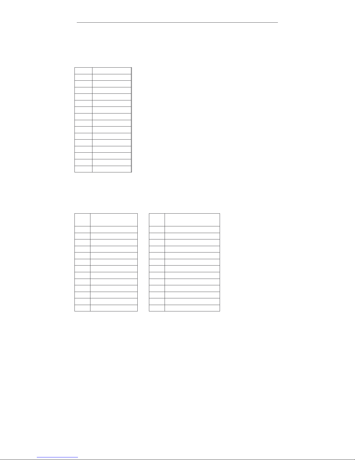
3.10. CRT VGA Connector on Front Panel (P24)
A standard DB-15 connector on front panel enables CRT display. This connector is
available only with the front panel option.
Pin Name
1 RED
2 GREEN
3 BLUE
4 N/C
5 GND
6 GND
7 GND
8 GND
9 N/C
10 GND
11 N/C
12 N/C
13 HSYNC
14 VSYNC
15 N/C
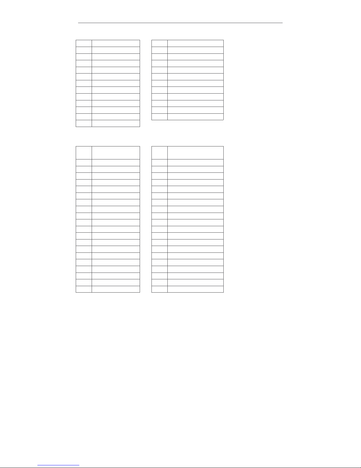
3.11. LCD Panel Connectors (P13, P20)
P13 - 51-pos FPC connector for LCD panels
Pin Name
Pin Name
01 LCD-VDD 27 LCD-VDD
02 LCD-VDD 28 LCD-VDD
03 LCD-R2 29 LCD-B2
04 LCD-R3 30 LCD-B3
05 GND 31 GND
06 LCD-R4 32 LCD-B4
07 LCD-R5 33 LCD-B5
08 GND 34 GND
09 LCD-R6 35 LCD-B6
10 LCD-R7 36 LCD-B7
11 GND 37 GND
12 LCD-R0 38 LCD-B0
13 LCD-R1 39 LCD-B1
Page 19
SB-X270 PC/104+ Single Board Computer
CompuLab LTD.
19
14 GND 40 GND
15 GND 41 GND
16 LCD-G2 42 LCD-LP
17 LCD-G3 43 LCD-FRM
18 GND 44 LCD-DE
19 LCD-G4 45 GND
20 LCD-G5 46 LCD-SCK
21 GND 47 GND
22 LCD-G6 48 LCD-ENVDD
23 LCD-G7 49 LCD-ENVEE
24 GND 50 LCD-VDD
25 LCD-G0 51 LCD-VDD
26 LCD-G1
P20 - 40-pin FPC connector for TFT panels
Pin Name
Pin Name
01 NC 21 LCD-VDD
02 LCD-VDD-EN 22 TSPY
03 GND 23 TSMY
04 LCD-R0 24 TSPX
05 LCD-R1 25 TSMX
06 LCD-VDD 26 LCD-B0
07 LCD-R2 27 LCD-VDD
08 LCD-R3 28 LCD-B1
09 GND 29 LCD-B2
10 LCD-R4 30 GND
11 LCD-R5 31 LCD-B3
12 LCD-VDD 32 LCD-B4
13 LCD-G5 33 GND
14 LCD-G4 34 LCD-B5
15 GND 35 LCD-DE
16 LCD-G3 36 LCD-VDD
17 LCD-G2 37 LCD-LP
18 LCD-VDD 38 LCD-FRM
19 LCD-G1 39 GND
20 LCD-G0 40 LCD-SCK
LCD-VDD-EN is an active low ENAVDD signal to be used in conjunction with the
CONLCD-GEN-V2 adapter module, available from CompuLab.
Page 20
SB-X270 PC/104+ Single Board Computer
CompuLab LTD.
20
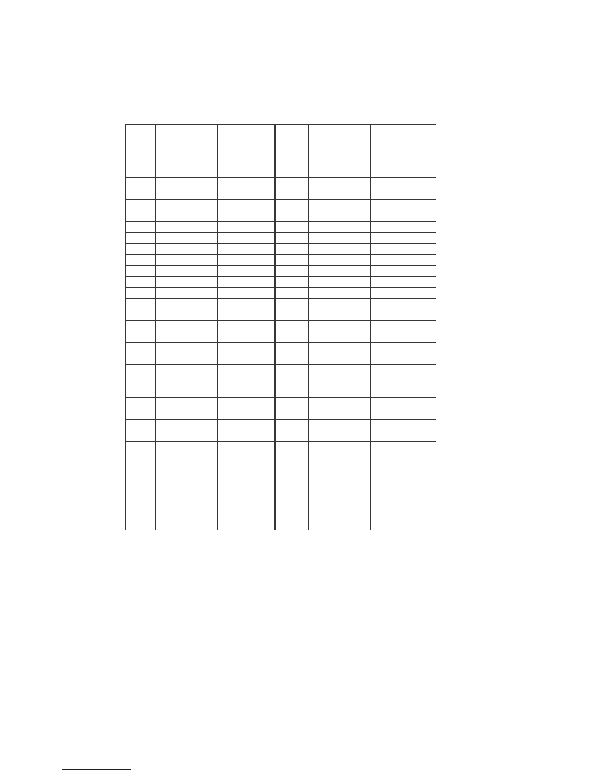
3.12. PC/104 connector (P4)
A PC/104 (ISA bus type) stackthrough connector provides limited ISA-like functionality.
The CM-X270's local bus lines are connected through buffers to their respective
counterparts on the PC/104 connector.
Pin
PC/104
Signal
CM-X270
connector
pin name
Pin PC/104
Signal
CM-X270
connector
(or other
origin) name
A01 IOCHCHK# - B01 GND GND
A02 SD7 LB-D7 B02 RESETDRV RSTDRV
A03 SD6 LB-D6 B03 +5V VCC5
A04 SD5 LB-D5 B04 IRQ9 A05 SD4 LB-D4 B05 -5V A06 SD3 LB-D3 B06 DRQ2 A07 SD2 LB-D2 B07 -12V A08 SD1 LB-D1 B08 0WS# A09 SD0 LB-D0 B09 +12V A10 IOCHRDY LB-IORDY B10 KEY A11 AEN GND B11 SMEMW# ISA-WR#*
A12 SA19 LB-A19 B12 SMEMR# ISA-RD#*
A13 SA18 LB-A18 B13 IOW# ISA-IOW#*
A14 SA17 LB-A17 B14 IOR# ISA-IOR#*
A15 SA16 LB-A16 B15 DACK3# Pullup
A16 SA15 LB-A15 B16 DRQ3 A17 SA14 LB-A14 B17 DACK1# Pullup
A18 SA13 LB-A13 B18 DRQ1 A19 SA12 LB-A12 B19 REFRESH Pullup
A20 SA11 LB-A11 B20 SYSCLK CLK8Mhz
A21 SA10 LB-A10 B21 IRQ7 A22 SA9 LB-A9 B22 IRQ6 A23 SA8 LB-A8 B23 IRQ5 GPIRQ1*
A24 SA7 LB-A7 B24 IRQ4 A25 SA6 LB-A6 B25 IRQ3 GPIRQ1*
A26 SA5 LB-A5 B26 DACK2# Pullup
A27 SA4 LB-A4 B27 TC GND
A28 SA3 LB-A3 B28 BALE Pullup
A29 SA2 LB-A2 B29 +5V VCC5
A30 SA1 LB-A1 B30 OSC CLK16M hz
A31 SA0 LB-A21 B31 GND GND
A32 GND GND B32 GND GND
Page 21
SB-X270 PC/104+ Single Board Computer
CompuLab LTD.
21
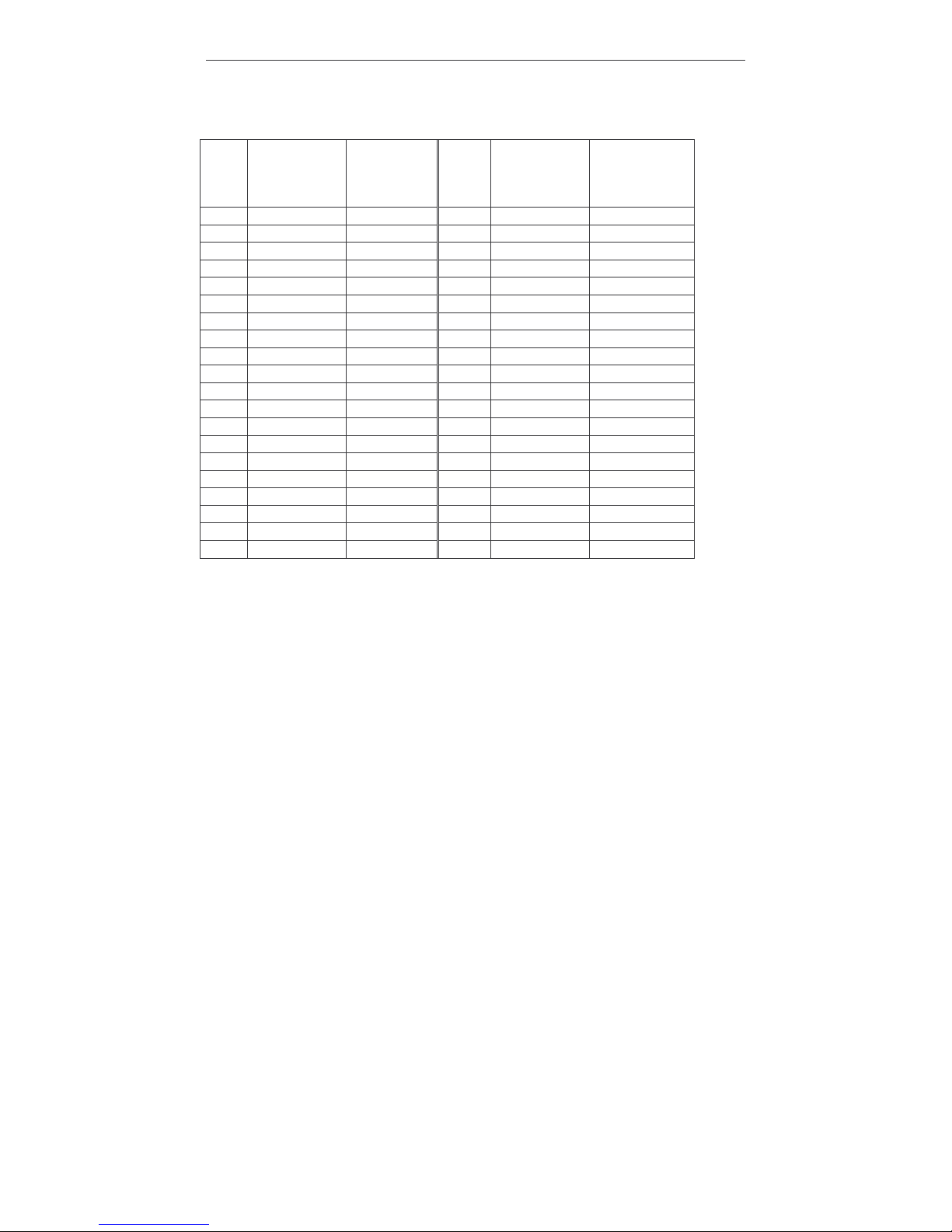
Pin
PC/104
Signal
CM-X270
connector
pin name
Pin PC/104
Signal
CM-X270
connector
pin name
C00 GND GND D00 GND GND
C01 SBHE# GND D01 MEMCS16# C02 LA23 LB-A23 D02 IOCS16# C03 LA22 LB-A22 D03 IRQ10 C04 LA21 LB-A21 D04 IRQ11 GPIRQ1*
C05 LA20 LB-A20 D05 IRQ12 C06 LA19 LB-A19 D06 IRQ15 GPIRQ1*
C07 LA18 LB-A18 D07 IRQ14 C08 LA17 LB-A17 D08 DACK0# Pullup
C09 MEMR# ISA-RD#* D09 DRQ0 C10 MEMW# ISA-WR#* D10 DACK5# Pullup
C11 SD8 LB-D8 D11 DRQ5 C12 SD9 LB-D9 D12 DACK6# Pullup
C13 SD10 LB-D10 D13 DRQ6 C14 SD11 LB-D11 D14 DACK7# Pullup
C15 SD12 LB-D12 D15 DRQ7 C16 SD13 LB-D13 D16 +5V
C17 SD14 LB-D14 D17 MASTER# Pullup
C18 SD15 LB-D15 D18 GND GND
C19 KEY - D19 GND GND
Signals marked in gray are not supported. In general, functionality of the PC104 bus of the
SB-X270 has the following limitations:
DMA channels are not supported.
Only four interrupt inputs are supported. B23, B25, D04, D06 pins are consolidated to
GPIRQ1 through OR gate.
Some signals of secondary importance are not supported: MEMSC16, IOCS16#,
BALE. The irrelevant signal REFRESH is also not supported.
Signals marked with (*) are generated by on-board logic. See section 4.3 for details.
The PXA-270 CPU does not support 8-bit granularity accesses. In order to make
attaching 8-bit PC-104 cards to the SB-X270 possible, LB-A21 was connected to SA0.
Page 22
SB-X270 PC/104+ Single Board Computer
CompuLab LTD.
22
3.13. PC/104+ PCI bus connector (P5)
Standard PC/104+ (PCI bus) connector. The CM-X270 PCI bus lines are directly
connected to the PC/104+ connector. All non-obvious connections are mentioned in notes.
Pin
Name Notes Pin Name Notes
A01 KEY2 N/C B01 (reserved)
A02 V I/O 3.3V B02 AD02
A03 AD05 B03 GND
A04 CBE0# B04 AD07
A05 GND B05 AD09
A06 AD11 B06 V I/O 3.3V
A07 AD14 B07 AD13
A08 +3.3V B08 CBE1#
A09 SERR# B09 GND
A10 GND B10 PERR#
A11 STOP# B11 +3.3V
A12 +3.3V B12 TRDY#
A13 FRAME# B13 GND
A14 GND B14 AD16
A15 AD18 B15 +3.3V
A16 AD21 B16 AD20
A17 +3.3V B17 AD23
A18 IDSEL0 AD28 via 150R B18 GND
A19 AD24 B19 CBE3#
A20 GND B20 AD26
A21 AD29 B21 +5.0V
A22 +5.0V B22 AD30
A23 REQ0# PCI-REQ0# B23 GND
A24 GND B24 REQ2# PCI-REQ2#
A25 GNT1# PCI-GNT1# B25 V I/O 3.3V
A26 +5.0V B26 CLK0
A27 CLK2 B27 +5.0V
A28 GND B28 INTD# PCI-INTD#
A29 +12V N/C B29 INTA# PCI-INTA#
A30 -12V N/C B30 (reserved)
Pin
Name Notes Pin Name Notes
C01 +5.0V D01 AD00
C02 AD01 D02 +5.0V
Page 23
SB-X270 PC/104+ Single Board Computer
CompuLab LTD.
23
C03 AD04 D03 AD03
C04 GND D04 AD06
C05 AD08 D05 GND
C06 AD10 D06 M66EN GND
C07 GND D07 AD12
C08 AD15 D08 +3.3V
C09 SB0# N/C D09 PAR
C10 +3.3V D10 SDONE N/C
C11 LOCK# D11 GND
C12 GND D12 DEVSEL#
C13 IRDY# D13 +3.3V
C14 +3.3V D14 CBE2#
C15 AD17 D15 GND
C16 GND D16 AD19
C17 AD22 D17 +3.3V
C18 IDSEL1 AD29 via 150R D18 IDSEL2 AD30 via 150R
C19 V I/O D19 IDSEL3 AD31 via 150R
C20 AD25 D20 GND
C21 AD28 D21 AD27
C22 GND D22 AD31
C23 REQ1# PCI-REQ1# D23 V I/O
C24 +5.0V D24 GNT0# PCI-GNT0#
C25 GNT2# PCI-GNT2# D25 GND
C26 GND D26 CLK1
C27 CLK3 D27 GND
C28 +5.0V D28 RST#
C29 INTB# PCI-INTB# D29 INTC# PCI-INTC#
C30 (reserved) D30 KEY2 N/C
Note
Due to limited amount of PCI request/grant pairs, the number of supported PC104+ slots is
limited. The availability of the slots depends on the module type and the presence of
RTL8139 Ethernet controller onboard the SB-X270 (option E), as described in the table
below. The numbers denote the amount of slots available for use.
SB-X270 "E"- option
E1 E2
CM-X270W 3 2
CM-X270L 2 1
Page 24
SB-X270 PC/104+ Single Board Computer
CompuLab LTD.
24
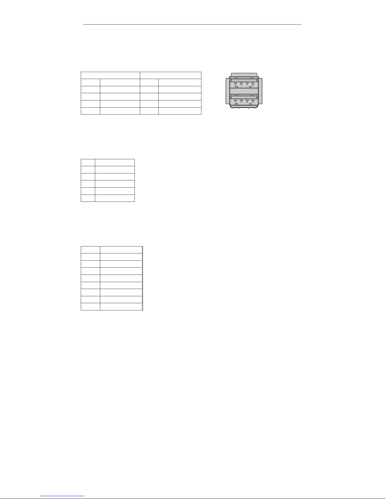
3.14. USB Dual Connector on Front Panel (U25)
A standard dual USB Type-A stacked connector on the front panel, used for USB1 and
USB3 interfaces.
USB interface 2 USB interface 1
Pin Name Pin Name
1 VBUS 5 VBUS
2 USB3-N 6 USB1-N
3 USB3-P 7 USB1-P
4 GND 8 GND
* USB3 can function either as Host or Slave (see P15).
3.15. Mini-USB type AB connector (P36)
A standard mini-USB Type-AB connector on the front panel, used for USB3 interface.
Pin Signal Name
1 USV_VCC
2 USB3-N
3 USB3-P
4 NC
5 GND
3.16. Ethernet Port 1 on Front Panel (P25)
A standard RJ45 connector provides an interface for the first Ethernet port available on the
CM-X270 module.
Pin Name
1 TXD+
2 TXD3 RXD+
4 5 6 RXD7 8 -
Page 25
SB-X270 PC/104+ Single Board Computer
CompuLab LTD.
25
3.17. Ethernet Port 2 on Front Panel (P26)
A standard RJ45 connector provides an interface for an Ethernet port implemented on the
SB-X270 board.
Pin Name
1 TXD+
2 TXD3 RXD+
4 5 6 RXD7 8 -
3.18. Ethernet FPC Connector (P11)
The Ethernet FPC connector is used as an alternative for the front panel Ethernet
connectors when the front panel is not available (as in standard PC/104 form factor). It is
impossible to use the FPC connector if the front panel connectors are assembled.
Ethernet FPC connector provides two separate groups of signals, one per Ethernet port
available in the CM-X270 / SB-X270 system.
Pin Name Pin Name
1 ETH1-LINK10# 11 ETH2-TX-VCC
2 ETH1-RDP 12 ETH2-TDP
3 ETH1-RDN 13 ETH2-TDN
4 ETH1-LINK10# 14 ETH2-TX-VCC
5 ETH1-LINK100# 15 ETH2-ACT#
6 ETH1-ACT# 16 ETH2-LINK100#
7 ETH1-TX-VCC 17 ETH2-LINK10#
8 ETH1-TDN 18 ETH2-RDN
9 ETH1-TDP 19 ETH2-RDP
10 ETH1-TX-VCC 20 ETH2-LINK10#
The connector matches with 20-wire 0.5 mm FPC cable. Ethernet signal routing is
implemented through the following scheme:
FPC connector >> FPC cable >> RJ45 module >> standard Ethernet cable
CompuLab provides the required FPC cables and RJ45 modules for single or dual Ethernet
ports. The modules include an FPC mating connector, one or two RJ45 connector/s with
transformer/s and activity LED's.
Page 26
SB-X270 PC/104+ Single Board Computer
CompuLab LTD.
26
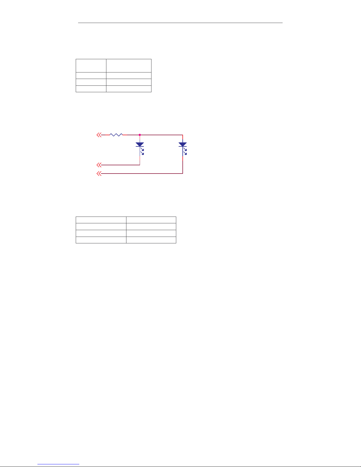
The default settings of activity LEDs for the SB-X270 on-board Ethernet interface are
specified in the table below. Settings can be changed by software.
Signal
Name
Indications
LED0 RX/TX activity
LED1 Link 100
LED2 Link 10
Note: LED signal wires in flat cable are also used as secondary shielding, so their
locations on the header may appear non-obvious.
The LED signal connections, as implemented in CompuLab's RJ-45 module, are:
DS5
LED-RED
DS4
LED-GREEN
LED2
R1
300R/1%
10M Link/Act
LED0
100M Link/Act
LED1
This connection supplies full information about speed / link / activity.
LED-RED: 100 Mbps activity indicator
LED-GREEN: 10 Mbps activity indicator
Activity LED (Red/Green)
none off
Link (only) on
Tx / Rx (and Link) blink
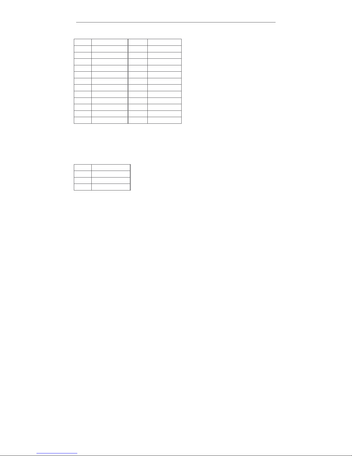
3.19. CIF - Camera Interface connector (P22)
P22 allows a connection of a CMOS sensor to the CM-X270 QuickCapture interface in
order to display/capture video stream and still images.
Page 27
SB-X270 PC/104+ Single Board Computer
CompuLab LTD.
27
Pin Name Pin Name
1 N/C 13 CLK-IN
2 GND 14 D6
3 SDA 15 GND
4 VCC2-5V 16 D5
5 SCL 17 PCLK
6 RST 18 D4
7 VSYNC 19 D0
8 N/C 20 D3
9 HSYNC 21 D1
10 VCC1-8V 22 D2
11 VCC3-3V 23 N/C
12 D7 24 N/C
3.20. Analog video input (P23)
A 1x3, 100 mil header provided for connecting analog video input to the Video Input
Processor available on the SB-X270
Pin Name
1 VID-IN1
2 GND
3 VID-IN2
Page 28
SB-X270 PC/104+ Single Board Computer
CompuLab LTD.
28
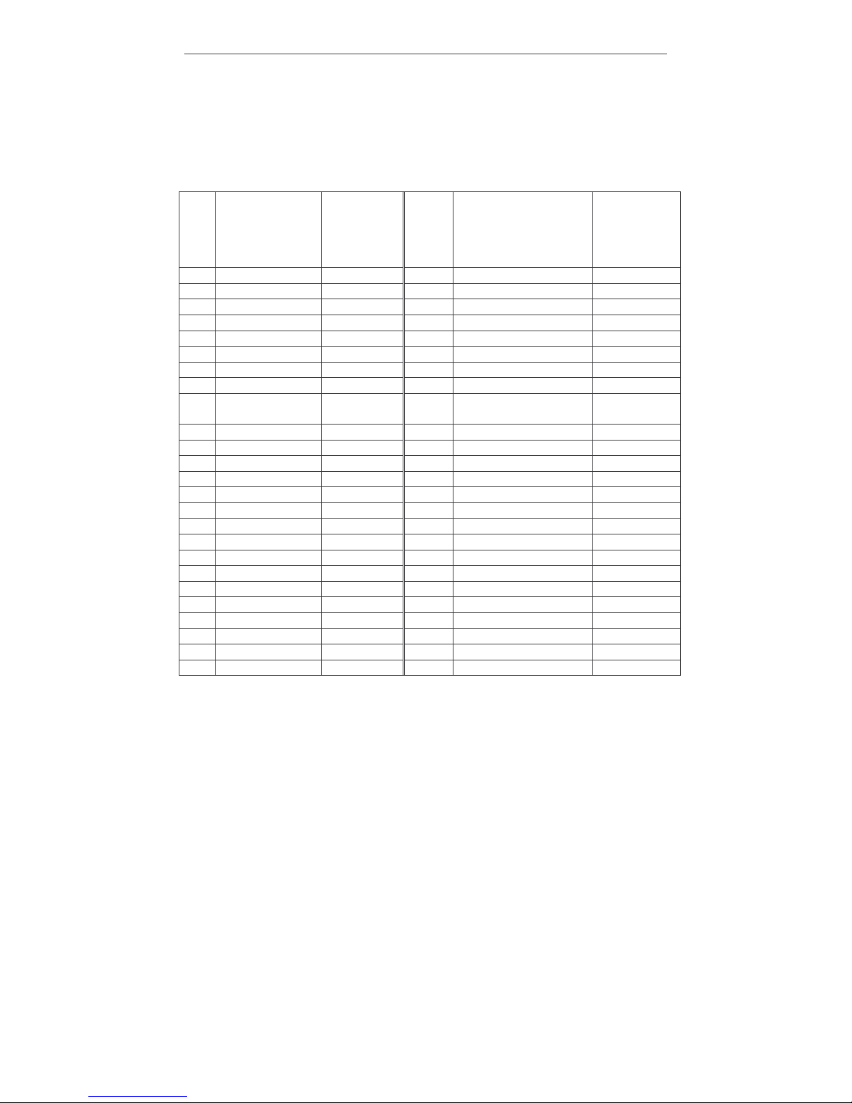
3.21. GPIO, COM ports and Special Functions (P16)
A 25x2 100 mil connector
Revision comment: pay attention that GPIO references in "Name" column were changed to
match those of PXA270.
Pin Name
GPIO
reference
in SB-X270
schematics
Pin Name GPIO
reference
in SB-X270
schematics
01 VCC3-3 02 GPRS_LED_DRIVE
03 VCC-USIM 04 BT_LED_DRIVE
05 UIO 06 GPIO104 12
07 GPIO86 11 08 GPIO106 13
09 GPIO105 10 10 GPIO52 14
11 GPIO12 9 12 GPIO103 15
13 (reserved) 14 GPIO99 16
15 GPIO14 (45) 7 16 GPIO87 17
17 GPIRQ0 /
GPIO1
18 GPIO97 / DREQ1 18
19 VDD-FAULT# 20 VCC3-3
21 SYS-RST# 22 SYS-EN
23 PME# 24 GND
25 GPCS0# 26 GPIO19 (44) 5
27 GPCS1# 28 GPIO102 4
29 GPIO101 6 30 GND
31 COM-D-RX 32 COM-D-TX
33 COM-B-RTS# 34 COM-B-CTS#
35 COM-B-RX 36 COM-B-TX
37 SDA 38 SCL
39 RST-IN 40 GND
41 SSPCLK 42 SSPTXD
43 SSPFRM 44 SSPRXD
45 GPIO107 19 46 GND
47 RS485-TX-P 48 RS485-RX-P
49 RS485-TX-N 50 RS485-RX-N
Notes:
• GPIO reference in "Name" column - according to PXA270 naming.
• For SIM operation, a jumper should be assembled between pins 1 & 3.
• For GPIO 14(45) and 19(44) values in parentheses are for the CM-X270L module.
Page 29
SB-X270 PC/104+ Single Board Computer
CompuLab LTD.
29
• If pins 1-2 of E2 are shorted using a shunt jumper, GPIRQ1 and DREQ1 lines are not
driven by onboard buffers. With CM-X270W module, shorting pins 1-2 of E2 enables
the use of PXA270 GPIO101 and GPIO97.
• PXA270 GPIO 14, 19, 87, 102, 103 are available only with CM-X270W.
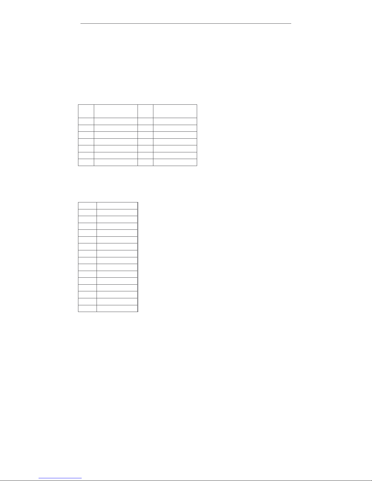
3.22. JTAG connector (P19)
A 7x2 100 mil connector. The CM-X270W JTAG interface is routed here.
Pin Name
Pin Name
01 VCC3_3SBY 02 GND
03 TRST# 04 GND
05 TDI 06 GND
07 TMS 08 GND
09 TCK 10 GND
09 TDO 10 RST_IN
09 VCC3_3SBY 10 GND
3.23. MMC/SDIO socket (P30)
The CM-X270 MMC/SDIO interface is connected to this standard MMC/SDIO socket.
Pin Name
1 DAT3
2 CMD
3 GND
4 VCC-SD
5 CLK
6 GND
7 DAT0
8 DAT1
9 DAT2
10 GND
11 CD
12 WP
13 GND
14 GND
15 GND
Page 30
SB-X270 PC/104+ Single Board Computer
CompuLab LTD.
30
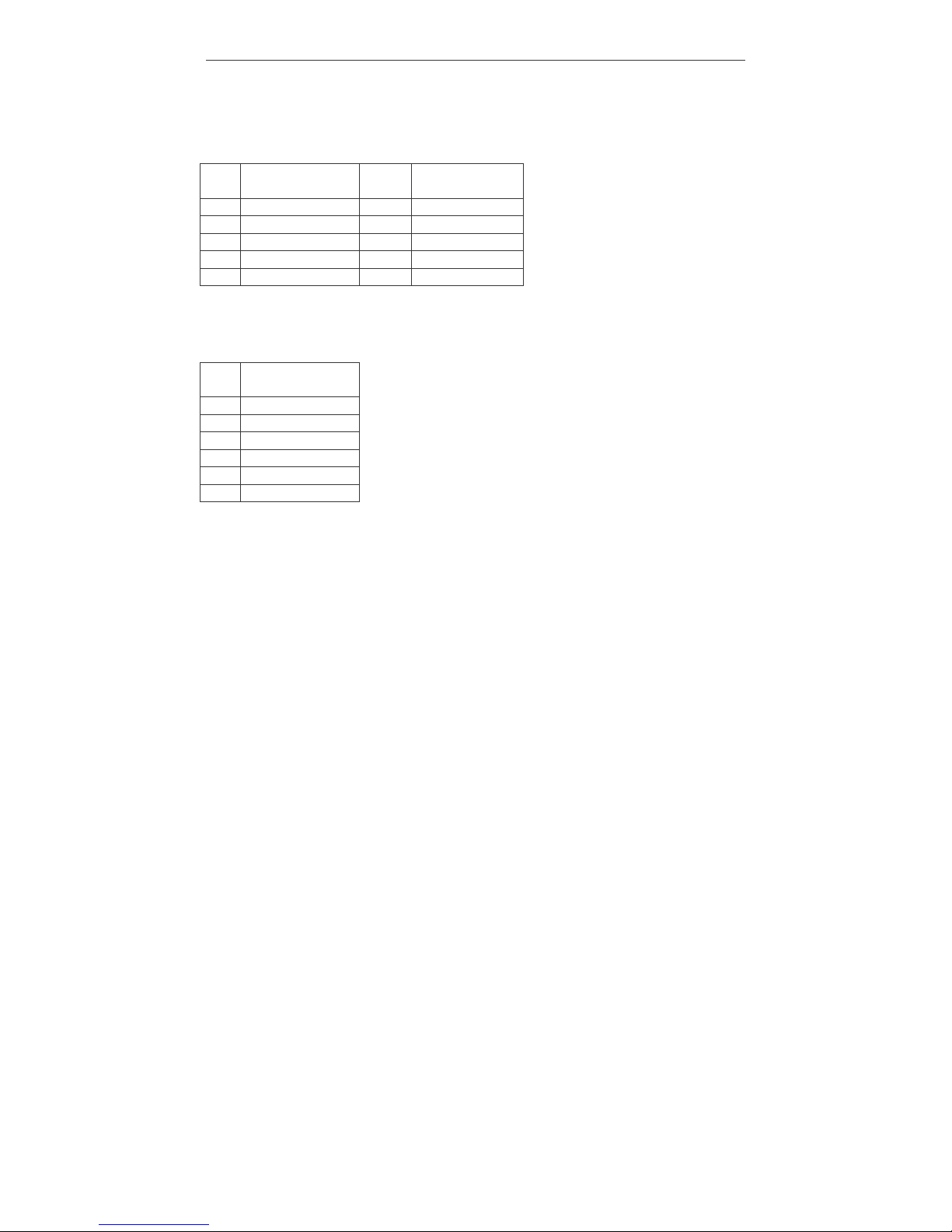
3.24. LPC connector (P17)
A 5x2 100 mil connector providing the CM-X270’s LPC interface
Pin Name
Pin Name
01 LAD0 02 LFRAME#
03 LAD1 04 SERIRQ
05 LAD2 06 VCC5
07 LAD3 08 LPC-CLK
09 GND 10 VCC3-3
3.25. P35 – A/D Input
Four A/D inputs available on the WM9715 AC’97 CODEC of the CM-X270W rev 2.
Pin Name
01 AD4
02 AD3
03 GND
04 AD2
05 AD1
06 GND
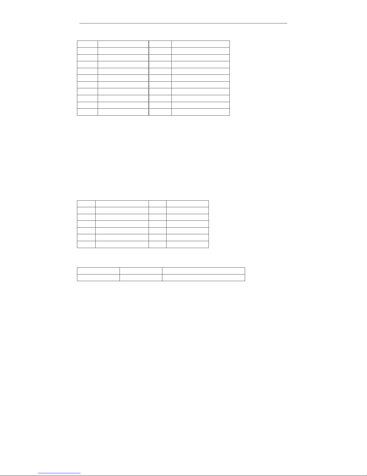
3.26. VGA & COM-A FPC Connector (P31)
The VGA & COM-A FPC connector provides two separate groups of signals, one for a
COM-A serial port and another for a VGA (analog RGB) output. Two different groups of
signals are consolidated in order to save board space. This connector delivers the same
signals as are routed to the front panel. It can be used whether the front panel is assembled
or not.
Page 31
SB-X270 PC/104+ Single Board Computer
CompuLab LTD.
31
Pin Name Pin Name
1 COM-A-DCD 11 HSYNC
2 COM-A-RX 12 GND
3 COM-A-TX 13 VSYNC
4 COM-A-DTR 14 GND
5 GND 15 BLUE
6 COM-A-DSR 16 GND
7 COM-A-RTS 17 GREEN
8 COM-A-CTS 18 GND
9 COM-A-RI 19 RED
10 GND 20 GND
The connector matches with a 20-wire FPC cable. Signal routing is implemented through
the following scheme:
FPC conn >> FPC cable >> DB15 & DB9 Interface module >> standard VGA and RS232 cables
CompuLab provides VGA and RS232 interface modules in three varieties: a VGA only
module with DB15 connector, a RS232 only module with DB9 connector and a combined
module with both connectors.
3.27. SIM Card Socket (P12)
Connector P12, standard SIM card socket:
Pin Signal Name Pin Signal Name
1 GPRS_SIMVCC 7 GPRS_SIMIO
2 GPRS_SIMRST 8 GND
3 GPRS_SIMCLK 9 GND
4 - 10 GND
5 GND 11 GND
6 NC
Reference connector data:
Manufacturer Mfg. P/N Mating connector
Astron 5190006-006-R Standard SIM card.
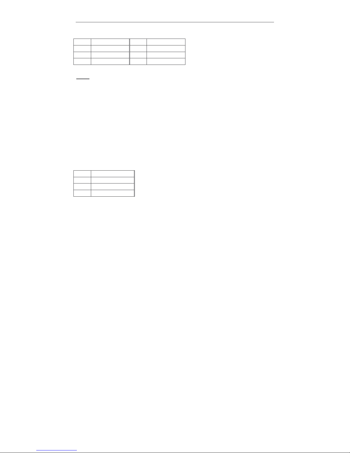
3.28. Power Connectors
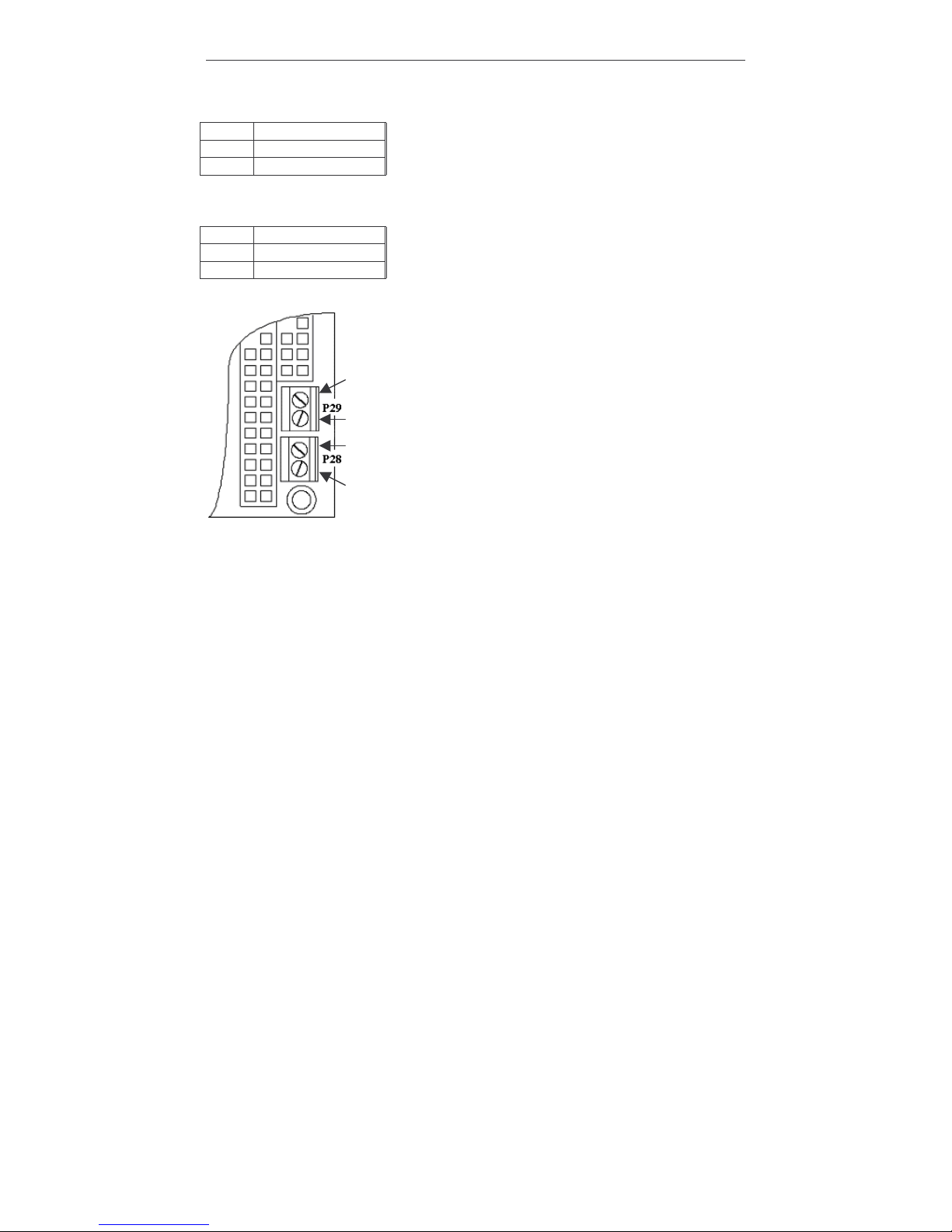
P29: The 2-node terminal block is used as a main power connector.
Page 32
SB-X270 PC/104+ Single Board Computer
CompuLab LTD.
32
Pin Name
1 VCC5
2 GND
P28: The 2-node terminal block is used as a low and high voltage power connector.
Pin Name
1 12V-48V
2 3.3V
GND
5V
3.3V
48V
Page 33
SB-X270 PC/104+ Single Board Computer
CompuLab LTD.
33
4. Functions Implemented on the SB-X270
Most of the functions are implemented by the attached CM-X270 module, while the SBX270 board provides connectors or headers. Several additional functions are implemented
on the SB-X270 itself and are described in this section.
Note: The SB-X270 uses a CPLD (programmable logic IC) in order to implement
combinatory logic functionality. This is done in order to reduce component count and add
some flexibility to the design. The usage of a CPLD is not obligatory and can be replaced
by discrete logic IC’s. The internal design description of the CPLD is attached to the SBX270 schematics package.
4.1. PC/104 and IDE addressing and logic
The SB-X270 implements address decoding logic by GPCS and IDE-CS signals from the
CM-X270 for driving a number of control signals (OE#, WE#, CS#) to the PC/104 and
IDE buses. Below is a memory address map for the above buses and relevant active control
signals:
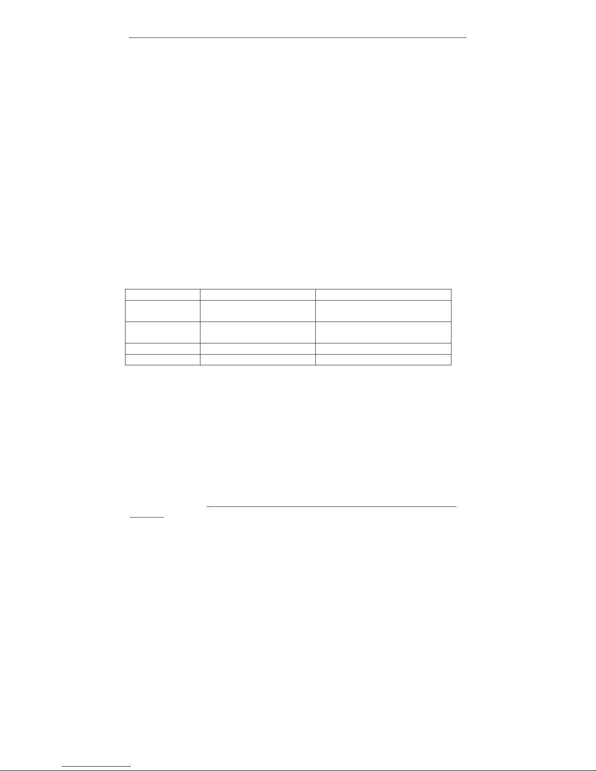
Description Address range Active control signals
PC/104 memory
access region
0x0C000000-0x0CFFFFFF ISA-RD#, ISA-WR#
PC/104 IO access
region
0x0D000000-0x0DFFFFFF ISA-IOR#, ISA-IOW#
IDE CS1 region 0x0E000000-0x0EFFFFFF IDE-CS#1, IDE-RD#, IDE-WR#
IDE CS0 region 0x0F000000-0x0FFFFFFF IDE-CS#0, IDE-RD#, IDE-WR#
4.2. PC-Card CardBus socket
The SB-X270 implements a custom solution allowing usage of standard 32bit CardBus
cards without a need for dedicated CardBus controller.
The cards are connected directly to the PCI bus and dedicated logic blocks the CBFRAME# signal during irrelevant PCI configuration cycles. The O/S drivers have been
slightly modified but, in general, the solution acts as a standard CardBus interface. The
CARDBUS-CTL signal is used to control the CB-FRAME# blocking. Please refer to the
SB-X270 schematics for implementation details. Only 3.3V PC-Cards are supported.
NOTE: this solution does not allow card insertion/removal (hot-plug) while the system is
powered.
Page 34
SB-X270 PC/104+ Single Board Computer
CompuLab LTD.
34
4.3. 10/100 Mbit Ethernet Port
The SB-X270 contains one optional 100 Mbit Ethernet port. This is in addition to the
optional Ethernet port contained in the CM-X270. The user can therefore order the CMX270 / SB-X270 combination with none, one or two Ethernet port(s). The Ethernet
interface is based on the Realtek RTL8139 chip.
The Ethernet port’s interface is either through the standard RJ45 connector on the front
panel or through 20-pin FPC connector P31. If the P31 interface used, the appropriate
FPC cable and RJ-45 module can be obtained from CompuLab.
4.4. RS-232 and RS-422/485 Serial Port Drivers
The CM-X270 module has on-board RS-232 drivers for the COM-A port. Other serial
ports of the CM-X270 have TTL level interfaces. The SB-X270 adds several driver options
for some of the serial ports as specified in the table below. Driver support includes modem
control lines.
Level options
Port Modem
control
CM-X270
name
Origin
RS
232
RS
422/485
TTL
COM-A + COM-A PXA270 + - COM-B - COM-B PCI bridge + - +
COM-C + COM-C PXA270 + + +
COM-D - COM-D PXA270 + - +
Notes
COM-D is shared with the IR port.
If the SB-X270 is assembled with no drivers for a particular COM port, then the port
signals are available with TTL levels (except for COM-A).
The interface of the COM-C port can be either RS-232 or RS-422/485 or both,
controlled by assembling the appropriate driver chips. Assembling is done according to
the SB-X270's configuration code: [none] - drivers not assembled, "Y2" - only RS-232
drivers assembled, "Y4" - only RS422/485 drivers assembled, "Y6" - both RS-232 and
RS-422/485 drivers assembled.
RS-422 and RS-485 modes of COM-C
Page 35

SB-X270 PC/104+ Single Board Computer
CompuLab LTD.
35
The SB-X270 contains RS-422/485 drivers if its configuration code has the "Y4" or "Y6"
option. In the case of "Y6" option, when both RS-232 and RS422/485 drivers are present,
the SB-X270 will automatically switch into RS-232 mode on the presence of valid voltage
levels on RS-232 RX input. In the absence of valid input, the card will switch to RS422/485 mode.
In RS-422/485 modes, TXD outputs of the COM-C port are enabled by the RTS2 signal.
RTS "1" level enables TX output, RTS "0" disables it.
In RS-485 (half duplex) mode, transmit and receive operations are performed on TX lines.
To achieve this, the user must physically connect the RX and TX lines of the serial driver,
i.e., RX+ to TX+ and RX- to TX-. In this case, the selection between receive and transmit
operations is performed by RTS.
In RS-422 (full duplex) mode, transmit and receive operations are performed on separate
line pairs. TX output can always be enabled, though qualifying it by RTS has no practical
effect on system operation. RX and TX lines should not be connected together as in the
case of RS-485.
For a better understanding of RS-422/485 driver operation, please refer to the SB-X270
design schematics, available following the [developer] >> [X270] links in CompuLab's
web-site.
4.5. LCD Power Switch and VDD selection
The graphics controller for TFT panels is located on the CM-X270 module. The SB-X270
adds the power switch required for certain LCD panels.
Many LCD panels require proper power sequencing in order to avoid panel damage. The
graphics controller of the CM-X270 module provides the LCD-ENVDD signal, which can
be used to indicate when power should be applied. The LCD-ENVDD signal is AND'ed
with the system’s RESET-OUT# signal. The LCD power switch circuit on the SB-X270
applies a VDD on the LCD interface connector under the control of ENVDD and RESETOUT# .
LCD Supply selection: the user can select 3.3V or 5V supply by a jumper on the P15
header, pins 1-2 for 3.3V or 2-3 for 5V.
Note: although it is possible to supply 5V to the LCD, the CM-X270 supplies LCD signals
at a 3.3V level. The LCD should be compatible with these levels in order to operate
properly.
Page 36
SB-X270 PC/104+ Single Board Computer
CompuLab LTD.
36
4.6. Power Supply Options
Supply voltage options are:
1. 5V only
In this case, 3.3V is generated on-board, by a step-down converter.
Note: additional cards, like PC/104+ or PCMCIA should not draw more than 3A from
3.3V.
2. 3.3V and 5.0V
3.3V and 5V can be supplied via the power connectors or PC/104+ connector.
3. 12V-48V input
The "S48" option allows the assembly of a versatile step-down switching converter. It
permits unregulated DC input in the range of 12V-48V and delivers a regulated 5V
supply to the system. Connector P28 should be used for high-voltage DC input.
GSM / GPRS supply
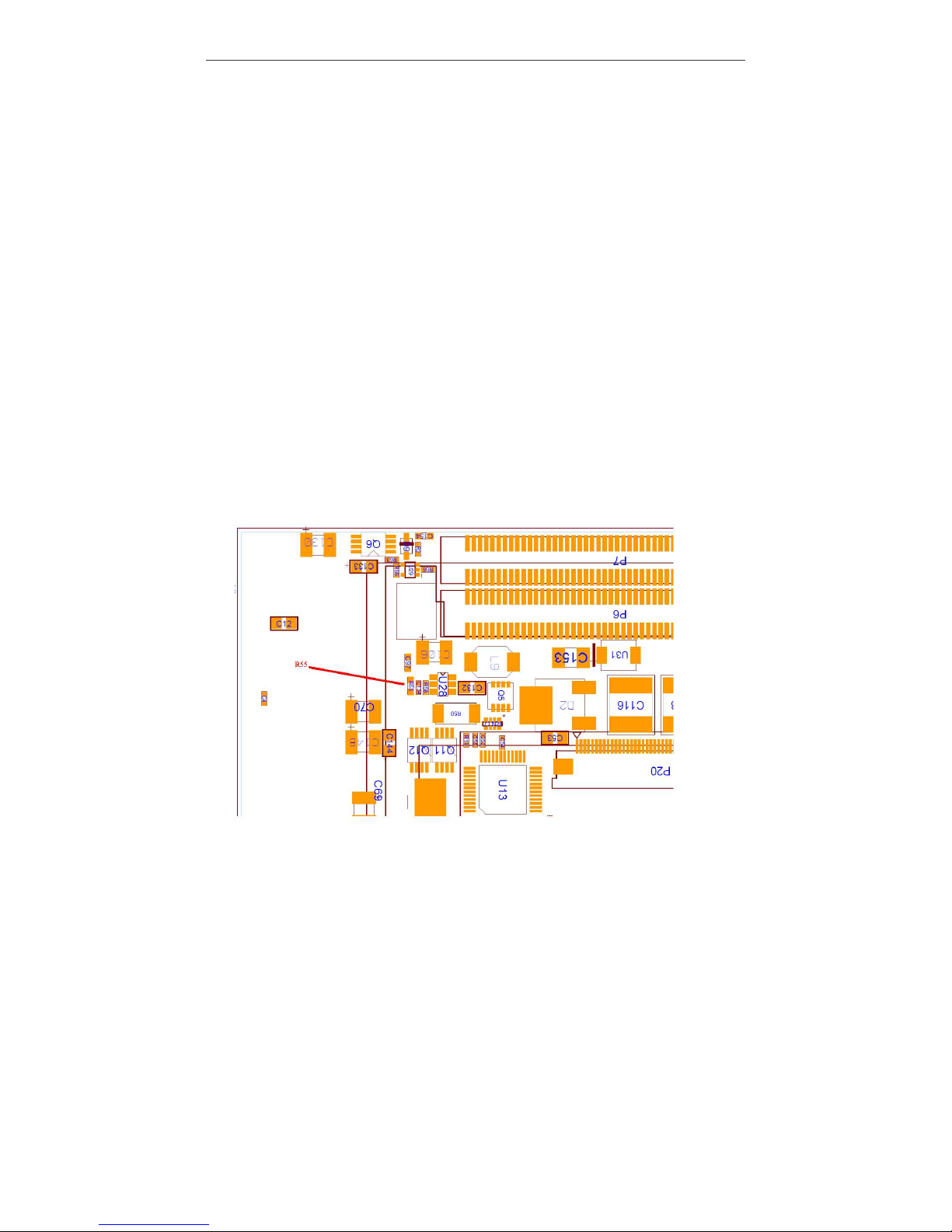
CM-X270W modules featuring the GSM / GPRS (K) option require 3.6V voltage for
proper operation. Replace R55 shown below with a 20k resistor to provide 3.6V to the
CM-X270. Cards are shipped by default voltage supply set to 3.3V rather than to 3.6V.
Without R55 modification, GSM / GPRS option would not work.
Page 37

SB-X270 PC/104+ Single Board Computer
CompuLab LTD.
37
4.7. CRT Interface - Video DAC
The SB-X270 implements an interface to CRT monitor by Video DAC, which converts
digital data of CM-X270's TFT output to analog RGB signals. Horizontal and vertical
synchronization signals are also generated from the TFT interface. All CRT interface
signals are routed to CRT connector P24 and FPC connector P31 as described in chapter 3.
4.8. Front Panel
The unique mechanical design of the SB-X270 allows selecting between two popular form
factors – either a standard PC/104+ with headers or an extended PC/104+ with front panel
connectors.
The SB-X270 printed circuit board has an extension used for the assembling of standard
connectors - two Ethernet ports, serial port, two USB ports and CRT monitor. If a front
panel is not required, this extension can be removed, either before assembling or even on
an already assembled card. If the front panel is removed, the SB-X270 remains fully
functional while the functions of front panel connectors are available through FPC
connectors P31 and P11.
Instructions for front panel removal
If you have the board with front panel and you need to remove it, follow these steps:
1. The board has the v-groove cut lines along the front panel, on the both sides of PCB.
Deepen these cut lines using sharp knife. Exert significant pressure. Be careful not to
hurt yourself !
2. Fix the front panel (the part to be removed) in carpentry vice.
3. Gently push the board backward and forward until it breaks along the cut line.
Note: trace wiring inside the PCB are designed to support this method of front panel
removal.
Page 38
SB-X270 PC/104+ Single Board Computer
CompuLab LTD.
38
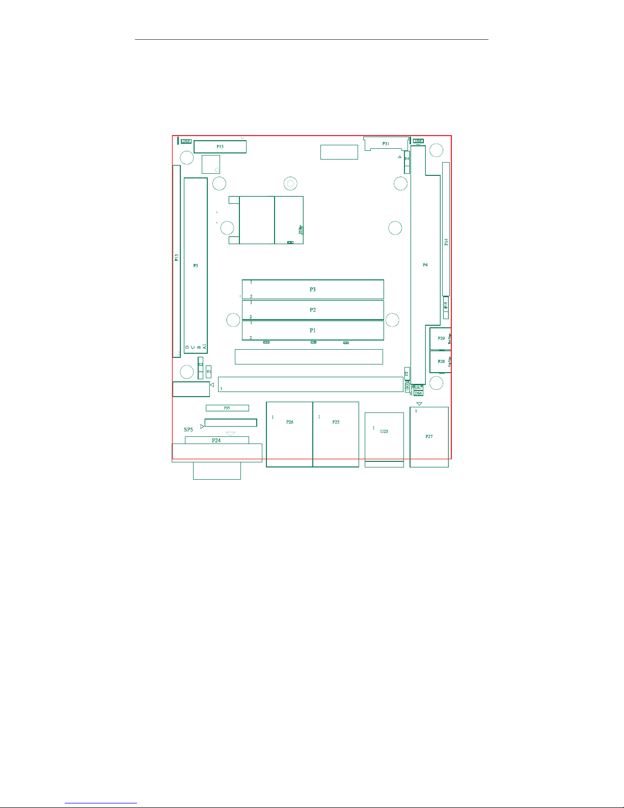
5. Connector Location
SB-X270 Top side
1
1
SB-X270
Rev1.3
P/N188C01153
1
1
1
2
1
3
SIM CARD
7
5
P16
SP3
P21
H8
H4
H6
P19
H9
H5
SW1
H2
H3
H7
P8
H1
P17
H10
P12
Page 39
SB-X270 PC/104+ Single Board Computer
CompuLab LTD.
39
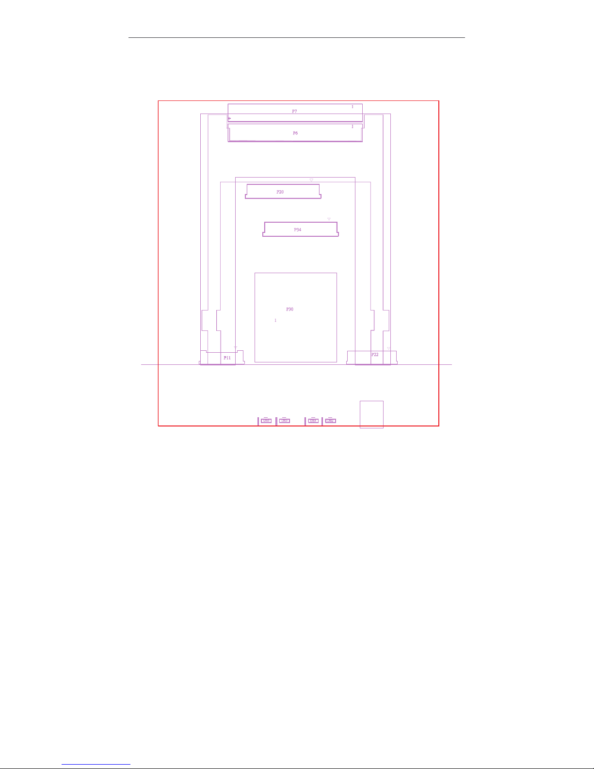
SB-X270 Bottom side
P36
P9
P10
Page 40

SB-X270 PC/104+ Single Board Computer
CompuLab LTD.
40
Reference
P1, P2, P3 Computer-on-module CAMI mating connectors
P4 PC/104 connector
P5 PC/104+ PCI bus connector
P6+P10 PC-Card PCMCIA socket
P7+P9 PC-Card CardBus socket
P8 IDE connector (100 mil)
P11 Ethernet Interface FPC connector
P12 SIM card socket
P13 LCD connector (51 pos FPC)
P14,P18 Audio, T/S and misc. connector
P15 USB and LCD supply selection connector
P16 GPIO and special functions
P17 LPC connector
P19 JTAG connector
P20 LCD connector (40 pos FPC)
P21 COM-C connector
P22 CIF (QuickCapture) connector
P24 CRT connector
P25 CoM Ethernet
P26 SB-X270 Ethernet
P27 COM-A connector
P28 Power connector (48V, 3.3V)
P29 Power connector (5V, GND)
P30 MMC/SDIO connector
P31 COM-A / CRT FPC connector
P34 IDE connector (40 pos FPC)
P35 A/D connector
P36 Mini-USB connector
E2 GPIO drive control
E3 CLOCK-OPTION
E4 PCMCIA power
U25 USB connector
DS1 IDE activity
DS2 CM-X270 Ethernet 100Mb Link/Act
DS3 SB-X270 Ethernet 100Mb Link/Act
DS4 CM-X270 Ethernet 10Mb Link/Act
DS5 SB-X270 Ethernet 10Mb Link/Act
DS6 VCC3-3 rail indicator
DS7 VCC5 rail indicator
DS8 GPRS status
Page 41
SB-X270 PC/104+ Single Board Computer
CompuLab LTD.
41
DS9 Bluetooth activity
SW1 Reset Switch
6. Operating Temperature Ranges
The SB-X270 is available with three options of operating temperature range:
Commercial 0o to 70o C
Extended -20o to 70o C
Industrial -40o to 85o C
The temperature testing and certification method is explained in the "Industrial
Temperature Support" page, available following the [Products] >> [Industrial
Temperature] links in CompuLab's web-site.
The mating CM-X270 should be ordered for the same temperature range as the SB-X270.
For example, it is not valid to use a SB-X270 manufactured for industrial temp range with
a CM-X270 manufactured for commercial temp range. Such a combination is practically
limited to the commercial temp range.
 Loading...