

Page 1

FACE MODULE
Design Guide
Page 2

© 2012 CompuLab
No warranty of accuracy is given concerning the contents of the information contained in this
publication. To the extent permitted by law no liability (including liability to any person by reason of
negligence) will be accepted by CompuLab, its subsidiaries or employees for any direct or indirect
loss or damage caused by omissions from or inaccuracies in this document.
CompuLab reserves the right to change details in this publication without notice.
Product and company names herein may be the trademarks of their respective owners.
CompuLab
P.O. Box 687 Yokneam Elite
20692 ISRAEL
Tel: +972 (4) 8290100
http://www.compulab.co.il
Fax: +972 (4) 8290126
Revised February 2012 FACE Module Design Guide 2
Page 3

Table of Contents
Table of Contents
1 INTRODUCTION .............................................................................................................. 5
1.1 About This Document ...................................................................................................... 5
1.2 Related Documents .......................................................................................................... 5
2 OVERVIEW ........................................................................................................................ 6
2.1 FACE Module Concept .................................................................................................... 6
3 FACE MODULE INTERFACES ...................................................................................... 7
3.1 PCIe .................................................................................................................................. 7
3.2 SATA ............................................................................................................................... 8
3.3 USB .................................................................................................................................. 8
3.4 SMBus .............................................................................................................................. 9
3.5 Digital Audio .................................................................................................................... 9
3.6 LPC .................................................................................................................................. 9
3.7 GPIOs ............................................................................................................................. 10
3.8 Power ............................................................................................................................. 10
3.9 Miscellaneous ................................................................................................................. 11
4 FACE MODULE CONNECTORS ................................................................................. 12
4.1 FACE Extension Connectors (PX1, PX2) ..................................................................... 12
5 ELECTRICAL DESIGN RECOMMENDATIONS ...................................................... 14
5.1 General Design Guidelines ............................................................................................ 14
5.2 PCIe Design Guidelines ................................................................................................. 14
5.3 SATA Design Guidelines ............................................................................................... 14
5.4 USB Design Guidelines ................................................................................................. 15
5.5 Power Supplies Design Guidelines ................................................................................ 15
6 MECHANICAL DESIGN CONSIDERATIONS .......................................................... 16
6.1 FACE Module PCB design ............................................................................................ 16
6.2 FACE Module Panel Design .......................................................................................... 17
Revised February 2012 FACE Module Design Guide 3
Page 4

Date
Description
January 2011
First release
Table 1 Document Revision Notes
Revised February 2012 FACE Module Design Guide 4
Page 5
Introduction
Document
Location
Fit-PC3 Resources
http://www.fitpc.com
FACE module design package
http://www.fitpc.com
1 INTRODUCTION
1.1 About This Document
This document is part of a set of reference documentation necessary to design and program custom
FACE modules for CompuLab products.
1.2 Related Documents
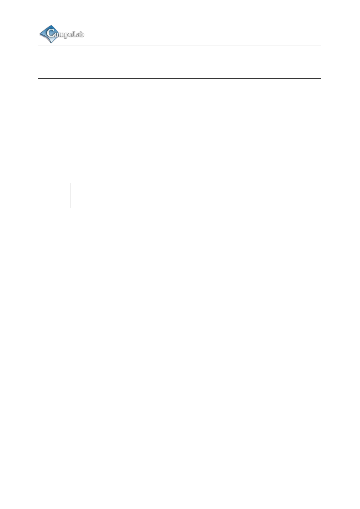
For additional information not covered in this document, please refer to the documents listed in Table
2.
Table 2 Related Documents
Revised February 2012 FACE Module Design Guide 5
Page 6

Overview
2 OVERVIEW
2.1 FACE Module Concept
The CompuLab product line of industrial PCs is designed to support custom functionality and I/O
extensions with FACE (Function And Connectivity Extension) modules.
FACE modules are implemented by an internal extension board and a simple sheet-metal panel. The
extension board is connected to the PC motherboard with two board-to-board connectors featuring
standard PC interfaces such as PCIe, USB2, SATA, SMBus etc.
This document outlines the FACE module interface specification and custom FACE module design
requirements and recommendations.
Revised February 2012 FACE Module Design Guide 6
Page 7
FACE Module interfaces
Signal Name
Pin #
Type
Description
Notes
PCIe-0
PCIE_P0_TX_P
PX1-A44
I/O
PCIe port 0 transmit positive
PCIE_P0_TX_N
PX1-A45
I/O
PCIe port 0 transmit negative
PCIE_P0_RX_P
PX1-B44
I/O
PCIe port 0 receive positive
PCIE_P0_RX_N
PX1-B45
I/O
PCIe port 0 receive negative
PCIe-1
PCIE_P1_TX_P
PX1-A41
I/O
PCIe port 1 transmit positive
PCIE_P1_TX_N
PX1-A42
I/O
PCIe port 1 transmit negative
PCIE_P1_RX_P
PX1-B41
I/O
PCIe port 1 receive positive
PCIE_P1_RX_N
PX1-B42
I/O
PCIe port 1 receive negative
PCIe-2
PCIE_P2_TX_P
PX1-A38
I/O
PCIe port 2 transmit positive
PCIE_P2_TX_N
PX1-A39
I/O
PCIe port 2 transmit negative
PCIE_P2_RX_P
PX1-B38
I/O
PCIe port 2 receive positive
PCIE_P2_RX_N
PX1-B39
I/O
PCIe port 2 receive negative
PCIe-3
PCIE_P3_TX_P
PX1-A35
I/O
PCIe port 3 transmit positive
PCIE_P3_TX N
PX1-A36
I/O
PCIe port 3 transmit negative
PCIE_P3_RX_P
PX1-B35
I/O
PCIe port 3 receive positive
PCIE_P3_RX_N
PX1-B36
I/O
PCIe port 3 receive negative
PCIe generic
PCIE_CLK1_P
PX1-B32
O
PCIe clock 1 positive
PCIE_CLK1_N
PX1-B33
O
PCIe clock 1 negative
PCIE_CLK2_P
PX2-B26
O
PCIe clock 2 positive
PCIE_CLK2_N
PX2-B27
O
PCIe clock 2 negative
PCIE_RESET#
PX1-B31
O
PCIe reset. Asserted during transition to
S3/S4/S5.
PCIE_WKUP#
PX1-A37
I
PCIe wake-up
PCIE_CLKREQ#
PX2-A41
I
PCIe clock request
3 FACE MODULE INTERFACES
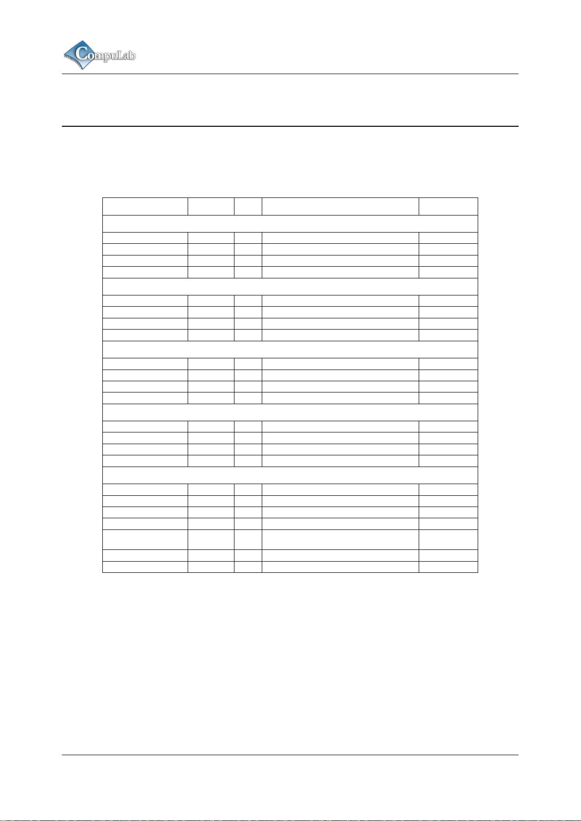
3.1 PCIe
Table 3 PCIe Interface Signals
Revised February 2012 FACE Module Design Guide 7
Page 8
FACE Module interfaces
Signal Name
Pin #
Type
Description
Notes
SATA-1
SATA_P1_TX_P
PX1-B8
O
SATA channel 1 transmit positive
SATA_P1_TX_N
PX1-B9
O
SATA channel 1 transmit negative
SATA_P1_RX_P
PX1-B11
I
SATA channel 1 receive positive
SATA_P1_RX_N
PX1-B12
I
SATA channel 1 receive negative
SATA-2
SATA_P2_TX_P
PX1-A2
O
SATA channel 2 transmit positive
SATA_P2_TX_N
PX1-A3
O
SATA channel 2 transmit negative
SATA_P2_RX_P
PX1-A5
I
SATA channel 2 receive positive
SATA_P2_RX_N
PX1-A6
I
SATA channel 2 receive negative
SATA-3
SATA_P3_TX_P
PX1-A8
O
SATA channel 3 transmit positive
SATA_P3_TX_N
PX1-A9
O
SATA channel 3 transmit negative
SATA_P3_RX_P
PX1-A11
I
SATA channel 3 receive positive
SATA_P3_RX_N
PX1-A12
I
SATA channel 3 receive negative
SATA generic
SATA_ACT#
PX1-B4
OD
SATA channel active
Signal Name
Pin #
Type
Description
Notes
USB-4
USB_P4_P
P1-A24
I/O
USB port 4 positive I/O
USB_P4_N
P1-A25
I/O
USB port 4 negative I/O
USB-5
USB_P5_P
PX2-A48
I/O
USB port 5 positive I/O
USB_P5_N
PX2-A49
I/O
USB port 5 negative I/O
USB-7
USB_P7_P
PX1-B17
I/O
USB port 7 positive I/O
USB_P7_N
PX1-B18
I/O
USB port 7 negative I/O
USB-8
USB_P8_P
PX1-B14
I/O
USB port 8 positive I/O
USB_P8_N
PX1-B15
I/O
USB port 8 negative I/O
USB-12
USB_P12_P
PX1-A27
I/O
USB port 12 positive I/O
USB_P12_N
PX1-A28
I/O
USB port 12 negative I/O
USB-13
USB_P13_P
PX2-A45
I/O
USB port 13 positive I/O
USB_P13_N
PX2-A46
I/O
USB port 13 negative I/O
USB Overcurrent
USB_P7_P8_OVC
PX1-B16
I/O
USB over current for ports 7 and 8
USB_P4_P12_OVC
PX1-A26
I/O
USB over current for ports 4 and 12
USB_P5_P13_OVC
PX1-A47
I/O
USB over current for ports 5 and 13
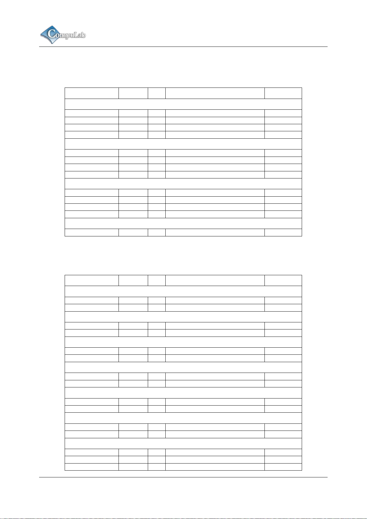
3.2 SATA
Table 4 SATA Interface Signals
3.3 USB
Table 5 PCIe Interface Signals
Revised February 2012 FACE Module Design Guide 8
Page 9
FACE Module interfaces
Signal Name
Pin #
Type
Description
Notes
SMBus-0
SMBUS_P0_CLK
PX1-A14
I/OD
SMBus channel 0 clock
SMBUS_P0_DAT
PX1-A15
I/OD
SMBus channel 0 data
SMBus-2
SMBUS_P2_CLK
PX2-A39
I/OD
SMBus channel 2 clock
SMBUS_P2_DAT
PX2-A40
I/OD
SMBus channel 2 data
SMBus thermal
SMBUS_THRM_CLK
PX2-B39
I/O
APU temperature sensor SMBus clock
SMBUS_THRM_DAT
PX2-B40
I/O
APU temperature sensor SMBus data
SMBus generic
SMBUS_ALERT#
PX1-A10
I/O
SMBus alert - this signal can be used to wake
the system or generate an SMI
Signal Name
Pin #
Type
Description
Notes
HDA_ RST#
PX1-A16
O
HD audio interface reset
HDA_SYNC
PX1-A17
O
HD audio sync signal to codec
HDA_CLK
PX1-A18
O
HD audio interface bit clock
HDA_SOUT
PX1-A19
O
HD audio serial data output to codec
HDA_SIN1
PX1-A20
I/O
HD audio serial data input from codec
HDA_SIN2
PX1-A21
I/O
HD audio serial data input from codec
Signal Name
Pin #
Type
Description
Notes
LPC_LAD0
PX1-A30
I/O
Multiplexed command / address / data bit 0
LPC_LAD1
PX1-A31
I/O
Multiplexed command / address / data bit 1
LPC_LAD2
PX1-A32
I/O
Multiplexed command / address / data bit 2
LPC_LAD3
PX1-A33
I/O
Multiplexed command / address / data bit 3
LPC_CLK
PX1-B23
O
33MHz clock for LPC devices
LPC_LFRAME#
PX1-B24
O
LPC bus frame
LPC_SER_IRQ
PX1-B22
I/O
Serial IRQ
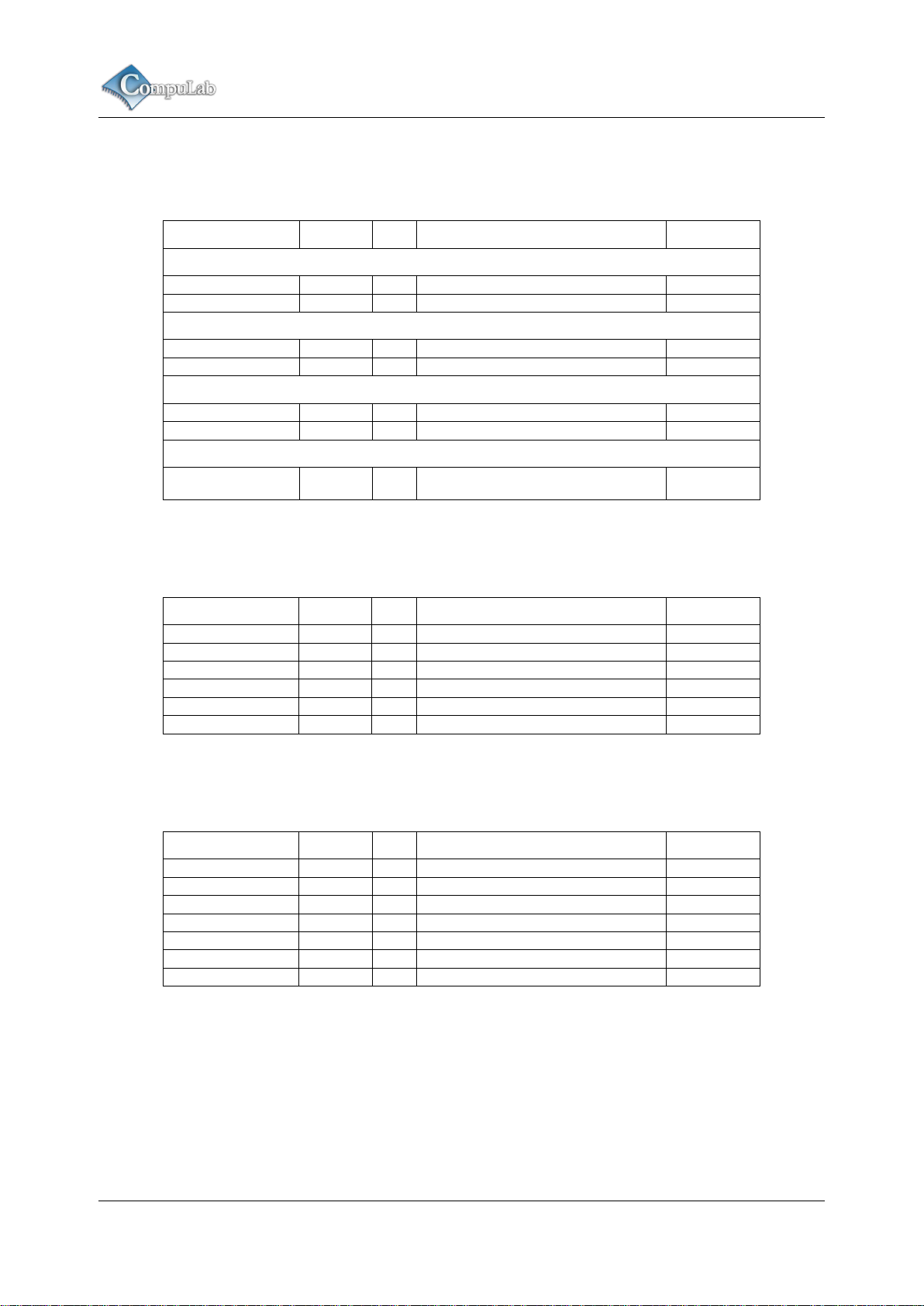
3.4 SMBus
Table 6 SMBus Interface Signals
3.5 Digital Audio
Table 7 Digital Audio Interface Signals
3.6 LPC
Table 8 LPC Interface Signals
Revised February 2012 FACE Module Design Guide 9
Page 10
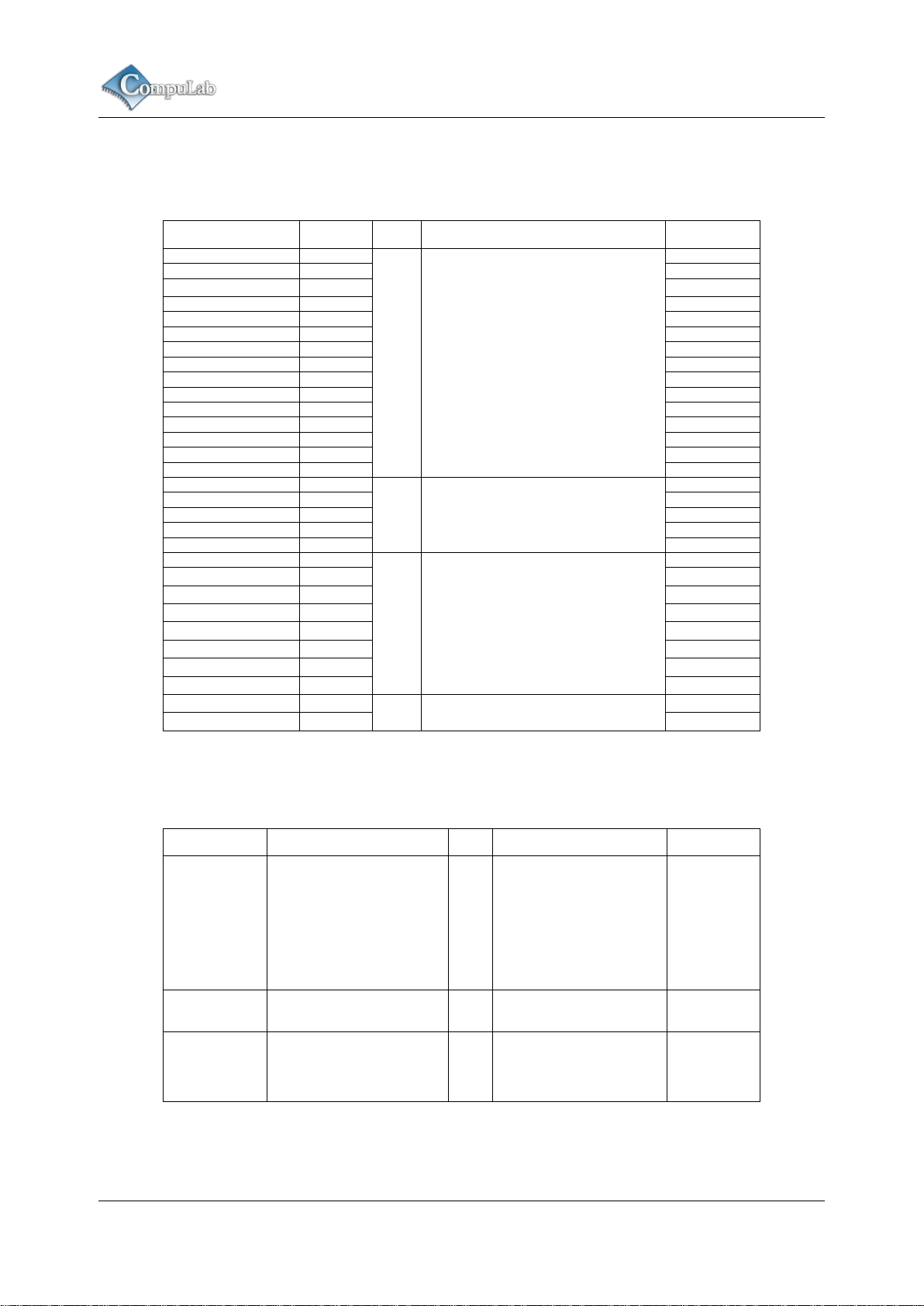
FACE Module interfaces
Signal Name
Pin #
Type
Description
Notes
FCH_GPIO0
PX2-B4
I/O
S0-domain General Purpose I/O
FCH_GPIO1
PX2-B10
FCH_GPIO3
PX2-B16
FCH_GPIO4
PX2-B12
FCH_GPIO5
PX2-B14
FCH_GPIO6
PX2-B15
FCH_GPIO7
PX2-B17
FCH_GPIO8
PX2-B18
FCH_GPIO9
PX2-B20
FCH_GPIO10
PX2-B21
FCH_GPIO11
PX2-B23
FCH_GPIO12
PX2-B24
FCH_GPIO54
PX1-A46
FCH_GPIO57
PX2-A42
FCH_GPIO58
PX2-A43
FCH_GPIO182
PX1-A22
I/O
S5-domain General Purpose I/O
FCH_GPIO201
PX2-A20
FCH_GPIO202
PX2-A21
FCH_GPIO204
PX2-A23
FCH_GPIO205
PX2-A24
FCH_GPIO129_OD
PX2-A17
I/OD
General Purpose I/OD
FCH_GPIO130_OD
PX2-A18
FCH_GPIO144_OD
PX2-A14
FCH_GPIO145_OD
PX2-A4
FCH_GPIO146_OD
PX2-A10
FCH_GPIO147_OD
PX2-A15
FCH_GPIO149_OD
PX2-A16
FCH_GPIO150_OD
PX2-A22
FCH_PWM0_GPIO197
PX2-B44
I/O
S5-domain General Purpose I/O
FCH_PWM1_GPIO198
PX2-B47
Signal Name
Pin #
Type
Description
Notes
GND
PX1-A1, PX1-B1, PX1-A7,
PX1-A23, PX1-B25, PX1-A29,
PX1-A34, PX1-A40, PX1-B40,
PX2-A1, PX2-B1, PX2-A7,
PX2-B7, PX2-A13, PX2-B13,
PX2-A25, PX2-B25, PX2-A32,
PX2-B32, PX2-A38, PX2-B41,
PX2-A44, PX2-A50
P
Main GND rail
5V_S5
PX1-B7, PX1-A13, PX1-B13,
PX1-B19, PX2-A19, PX2-B19
P
S5-domain 5V power rail
VCC_12V
PX1-A47, PX1-A48, PX1-A49,
PX1-A50, PX1-B47, PX1-B48,
PX1-B49, PX1-B50, PX2-B48,
PX2-B49, PX2-B50
P
Main 12V power rail
3.7 GPIOs
Table 9 GPIO Signals
3.8 Power
Revised February 2012 FACE Module Design Guide 10
Table 10 Power Signals
Page 11

FACE Module interfaces
Signal Name
Pin #
Type
Description
Notes
FACE_PRSNT#
PX1-B34
I
FACE module presence
detection. Must be connected
to GND.
PWR_BTN#
PX1-A43
I
Power button - causes an SMI
or SCI to indicate a system
request to enter a sleep state. If
the system is already in a sleep
state, this signal will cause a
wake event. If PWR_BTN# is
asserted for more than 4
seconds, it will cause an
unconditional transition (power
button override) to the S5 state
with only the PWR_BTN#
available as a wake event.
Override will occur even if the
system is in the S1 state. This
signal has an internal pull-up
resistor.
SLEEP_S3#
PX1-B43
O
S3 sleep power plane control.
Assertion of SLP_S3# shuts
off power to non-critical
components when system
transitions to S3, S4, or S5
states. De-assertion of
SLP_S3# turns on power to
non-critical components when
system transitions from S3, S4,
or S5 back to S0.
RESERVED
PX1-B2, PX1-B3, PX1-B5,
PX1-B6, PX1-B10, PX1-B20,
PX1-B26, PX1-B27, PX1-B28,
PX1-B29, PX1-B30, PX1-B37,
PX1-B46, PX2-A2, PX2-A3,
PX2-A5, PX2-A6, PX2-B2,
PX2-B3, PX2-B5, PX2-B6,
PX2-B28, PX2-B29, PX2-B30,
PX2-B31, PX2-A35, PX2-B33,
PX2-B34, PX2-B35, PX2-B36,
PX2-B37, PX2-B38, PX2-B42,
PX2-B43, PX2-B45, PX2-B46
-
Reserved for future use.
Should be left disconnected.
NC
PX2-A8, PX2-A9, PX2-A11,
PX2-A12, PX2-B8, PX2-B9,
PX2-B11, PX2-A26, PX2-A27,
PX2-A28, PX2-A29, PX2-A30,
PX2-A31, PX2-A33, PX2-A34,
PX2-A36, PX2-A37
-
Should be left disconnected.
3.9 Miscellaneous
Table 11 Miscellaneous Signals
Revised February 2012 FACE Module Design Guide 11
Page 12
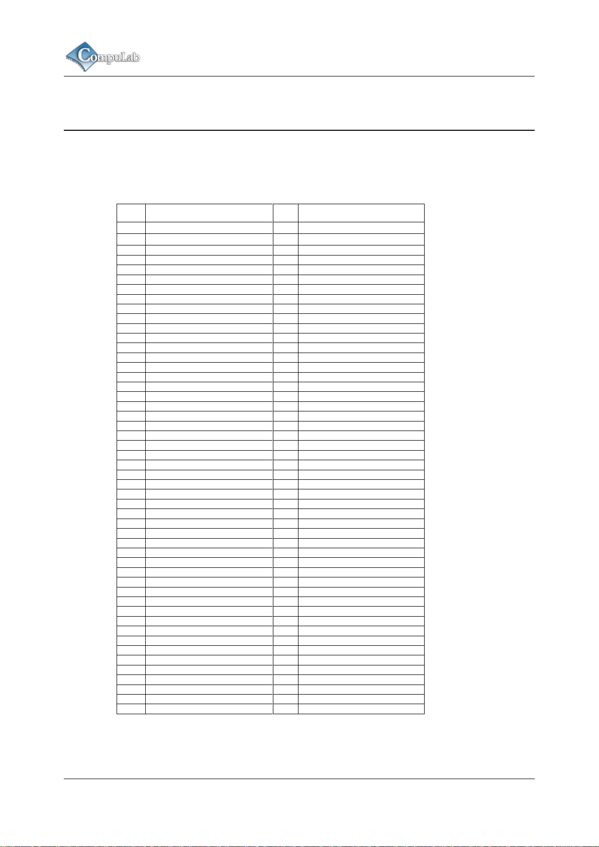
FACE MODULE Connectors
Pin
Signal Name
Pin
Signal Name
A1
GND
B1
GND
A2
SATA_P2_TX_P
B2
RESERVED
A3
SATA_P2_TX_N
B3
RESERVED
A4
IR RX
B4
SATA_ACT#
A5
SATA_P2_RX_P
B5
RESERVED
A6
SATA_P2_RX_N
B6
RESERVED
A7
GND
B7
5V_S5
A8
SATA_P3_TX_P
B8
SATA_P1_TX_P
A9
SATA_P3_TX_N
B9
SATA_P1_TX_N
A10
SMBALERT#
B10
RESERVED
A11
SATA_P3_RX_P
B11
SATA_P1_RX_P
A12
SATA_P3_RX_N
B12
SATA_P1_RX_N
A13
5V_S5
B13
5V_S5
A14
SMBUS_P0_CLK
B14
USB_P8_P
A15
SMBUS_P0_DAT
B15
USB_P8_N
A16
HDA_ RST#
B16
USB_P7_P8_OVC
A17
HDA_SYNC
B17
USB_P7_P
A18
HDA_CLK
B18
USB_P7_N
A19
HDA_SOUT
B19
5V_S5
A20
HDA_SIN1
B20
RESERVED
A21
HDA_SIN2
B21
IR TX
A22
FCH_GPIO182
B22
LPC_IRQ
A23
GND
B23
LPC_CLK
A24
USB_P4_P
B24
LPC_LFRAME#
A25
USB_P4_N
B25
GND
A26
USB_P4_P12_OVC
B26
RESERVED
A27
USB_P12_P
B27
RESERVED
A28
USB_P12_N
B28
RESERVED
A29
GND
B29
RESERVED
A30
LPC_LAD0
B30
RESERVED
A31
LPC_LAD1
B31
PCIE_RESET#
A32
LPC_LAD2
B32
PCIE_CLK1_P
A33
LPC_LAD3
B33
PCIE_CLK1_N
A34
GND
B34
FACE_PRSNT#
A35
PCIE_P3_TX_P
B35
PCIE_P3_RX_P
A36
PCIE_P3_TX N
B36
PCIE_P3_RX_N
A37
PCIE_WKUP#
B37
RESERVED
A38
PCIE_P2_TX_P
B38
PCIE_P2_RX_P
A39
PCIE_P2_TX_N
B39
PCIE_P2_RX_N
A40
GND
B40
GND
A41
PCIE_P1_TX_P
B41
PCIE_P1_RX_P
A42
PCIE_P1_TX_N
B42
PCIE_P1_RX_N
A43
PWR_BTN#
B43
SLEEP_S3#
A44
PCIE_P0_TX_P
B44
PCIE_P0_RX P
A45
PCIE_P0_TX_N
B45
PCIE_P0_RX_N
A46
FCH_GPIO54
B46
RESERVED
A47
VCC_12V
B47
VCC_12V
A48
VCC_12V
B48
VCC_12V
A49
VCC_12V
B49
VCC_12V
A50
VCC_12V
B50
VCC_12V
4 FACE MODULE CONNECTORS
4.1 FACE Extension Connectors (PX1, PX2)
Table 12 PX1 connector pin-out
Revised February 2012 FACE Module Design Guide 12
Page 13
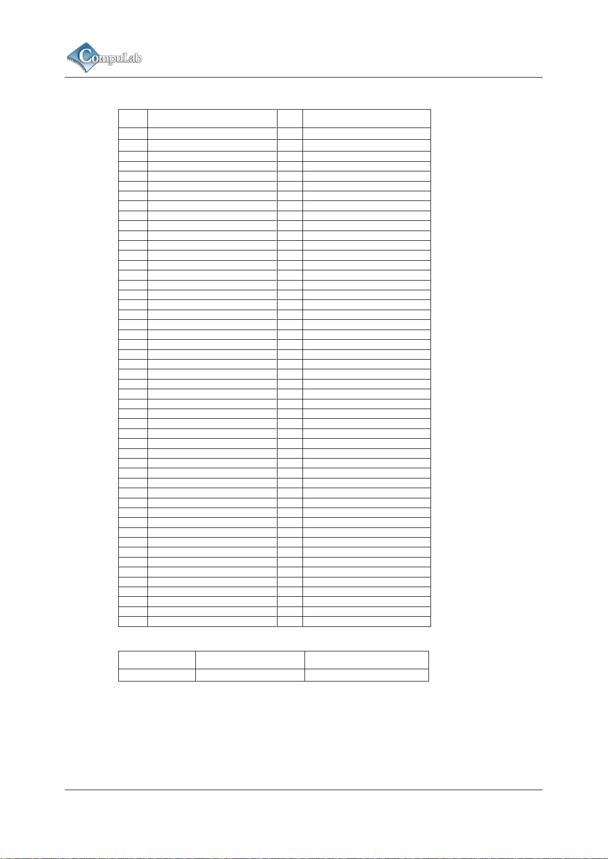
FACE MODULE Connectors
Pin
Signal Name
Pin
Signal Name
A1
GND
B1
GND
A2
RESERVED
B2
RESERVED
A3
RESERVED
B3
PCIE_P2_TX_N
A4
FCH_GPIO145_OD
B4
FCH_GPIO0
A5
RESERVED
B5
RESERVED
A6
RESERVED
B6
RESERVED
A7
GND
B7
GND
A8
NC
B8
NC
A9
NC
B9
NC
A10
FCH_GPIO146_OD
B10
FCH_GPIO1
A11
NC
B11
NC
A12
NC
B12
FCH_GPIO4
A13
GND
B13
GND
A14
FCH_GPIO144_OD
B14
FCH_GPIO5
A15
FCH_GPIO147_OD
B15
FCH_GPIO6
A16
FCH_GPIO149_OD
B16
FCH_GPIO3
A17
FCH_GPIO129_OD
B17
FCH_GPIO7
A18
FCH_GPIO130_OD
B18
FCH_GPIO8
A19
5V_S5
B19
5V_S5
A20
FCH_GPIO201
B20
FCH_GPIO9
A21
FCH_GPIO202
B21
FCH_GPIO10
A22
FCH_GPIO150_OD
B22
NC
A23
FCH_GPIO204
B23
FCH_GPIO11
A24
FCH_GPIO205
B24
FCH_GPIO12
A25
GND
B25
GND
A26
NC
B26
PCIE_CLK2_P
A27
NC
B27
PCIE_CLK2_N
A28
NC
B28
RESERVED
A29
NC
B29
RESERVED
A30
NC
B30
RESERVED
A31
NC
B31
RESERVED
A32
GND
B32
GND
A33
NC
B33
RESERVED
A34
NC
B34
RESERVED
A35
RESERVED
B35
RESERVED
A36
NC
B36
RESERVED
A37
NC
B37
RESERVED
A38
GND
B38
RESERVED
A39
SMBUS_P2_CLK
B39
SMBUS_THRM_CLK
A40
SMBUS_P2_DAT
B40
SMBUS_THRM_DAT
A41
PCIE_CLKREQ#
B41
GND
A42
FCH_GPIO57
B42
RESERVED
A43
FCH_GPIO58
B43
RESERVED
A44
GND
B44
FCH_PWM0_GPIO197
A45
USB_P13_P
B45
RESERVED
A46
USB_P13_N
B46
RESERVED
A47
USB_P5_P13_OVC
B47
FCH_PWM1_GPIO198
A48
USB_P5_P
B48
VCC_12V
A49
USB_P5_N
B49
VCC_12V
A50
GND
B50
VCC_12V
Manufacturer
Mfg. P/N
Mating connector
FCI
61082-10260[2|6]LF
61083-10460[2|6]LF
Table 13 PX2 connector pin-out
Revised February 2012 FACE Module Design Guide 13
Table 14 PX1, PX2 connector data
Page 14

Electrical design recommendations
5 ELECTRICAL DESIGN RECOMMENDATIONS
5.1 General Design Guidelines
Ensure that all VCC and GND power pins are connected.
Major power rails – VCC and GND must be implemented by planes, rather than by traces. Using
at least two planes is essential to ensure the system signal quality, as the planes provide a current
return path for all interface signals.
It is recommended to put several 100nF and 10/100uF capacitors between VCC and GND near
the FACE module interface connectors.
It is recommended to connect the standoff holes of the baseboard to GND, in order to improve
EMC.
Trace impedance of 50-55 Ω ± 15% should be maintained for single-ended signals unless
specified otherwise.
Pay attention to the current return paths (which are as important as the routing), length matching,
and signal spacing to maintain proper signal integrity.
Maintain a solid power and ground reference plane, and do not route high-speed signals across
plane splits. If plane-crossing is absolutely unavoidable, use a high frequency stitching capacitor
Refer to the reference schematic designs available in the FACE module design package.
5.2 PCIe Design Guidelines
One AC coupling (series) capacitor of 100nF is required on each PCIe receive signal.
AC coupling (series) capacitors for PCIe transmit and clock signals are located on the fit-PC3
motherboard. No capacitors are required on the FACE module PCB.
Capacitor packs are not allowed for AC coupling. Use only discrete capacitors.
The AC coupling capacitors should be located as close as possible to the PCIe device.
Target impedance for PCIe differential pairs should be 85 Ω ± 15%.
Trace spacing should be ≥ 4:1 on both sides of the pair.
Avoid stubs or test points on the signal pairs.
Please refer to the reference schematics and layout designs available in the FACE module design
package.
5.3 SATA Design Guidelines
AC coupling (series) capacitors for SATA signals are located on the fit-PC3 motherboard. No
capacitors are required on the FACE module PCB.
Target impedance for SATA differential pairs should be 90 Ω ± 10%.
Trace spacing should be ≥ 5:1 on both sides of the pair.
Avoid stubs or test points on the signal pairs.
Please refer to the reference schematics and layout designs available in the FACE module design
package.
Revised February 2012 FACE Module Design Guide 14
Page 15

Electrical design recommendations
5.4 USB Design Guidelines
No termination resistors are required.
Target impedance for USB differential pairs should be 90 Ω ± 15%.
Trace spacing should be ≥ 4:1 on both sides of the pair.
Avoid stubs or test points on the signal pairs.
Provide ESD suppression components for any USB pair that is accessible to the end user, and
optionally for any USB pair that is not accessible to the end user. No stubs are allowed from the
USB signals to the ESD components. Place these components between the common mode choke
and connector. It is recommended to place ESD suppression components as close as possible to
the connector and at no further than 0.5” from the connector body.
Decouple the ESD suppression component with a high frequency capacitor placed directly across
the device power and GND pins, no further than 50 mils away.
Provide the option for a common mode choke for EMI suppression for any USB pairs that can be
connected to cabled devices. The chokes should be bypassed with 0-Ω resistors by default. The
resistors must be located under the choke to minimize stubs. Place the choke within 1.0” of the
USB connector.
Please refer to the reference schematics and layout designs available in the FACE module design
package.
5.5 Power Supplies Design Guidelines
Implement FACE module power supply rails with DC-DC switching regulators.
12V power rail should be used to supply the FACE module DC-DC switching regulators.
Maximal current consumption from the 12V power rail should not exceed 1A.
Maximal current consumption from the 5V power rail should not exceed 2A.
SLP_S3# signal may be utilized to implement power supply control. Please note SLP_S3#
polarity requirements.
Please refer to the reference schematics and layout designs available in the FACE module design
package.
Revised February 2012 FACE Module Design Guide 15
Page 16
Mechanical design considerations
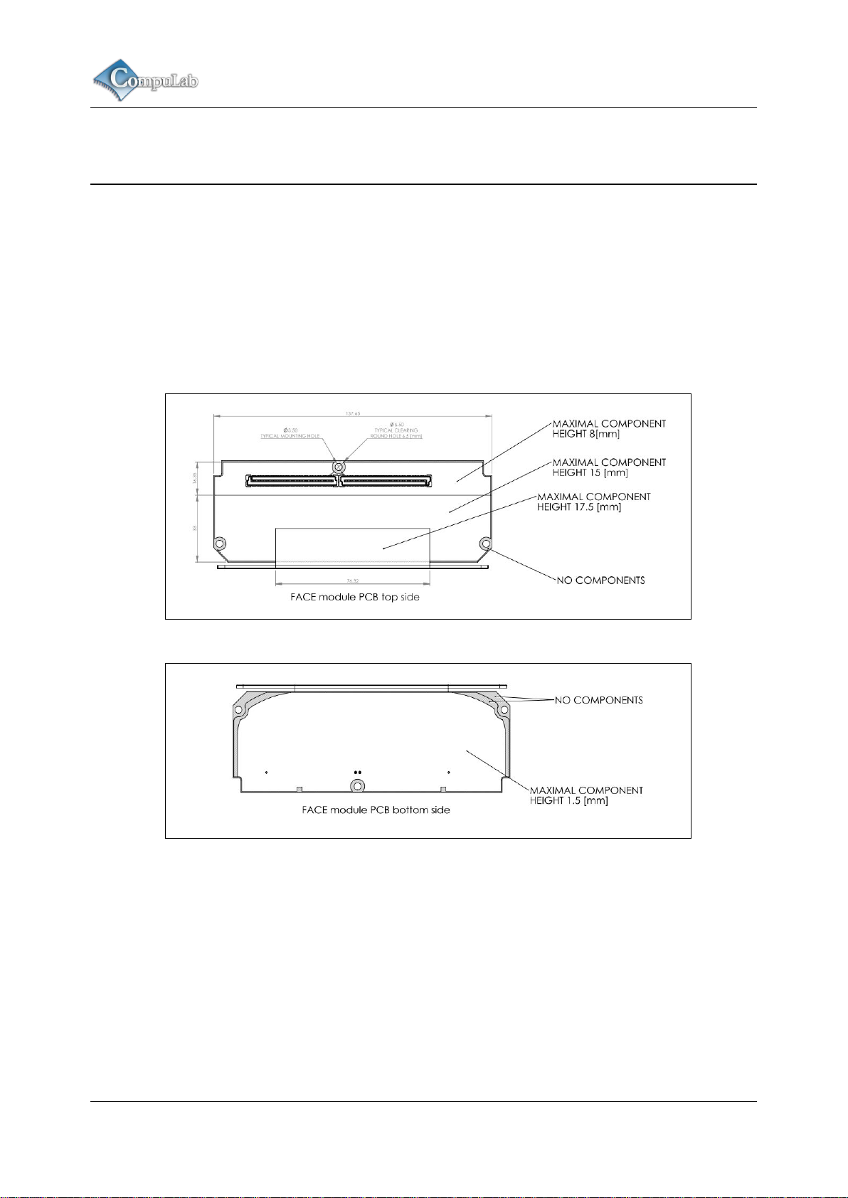
6 MECHANICAL DESIGN CONSIDERATIONS
6.1 FACE Module PCB design
The mechanical drawings below specify component placement restrictions.
Full mechanical drawings are available as part of the “FACE module design package” at
http://www.fit-pc.com/.
Figure 1 FACE module PCB top
Figure 2 FACE module PCB bottom
Revised February 2012 FACE Module Design Guide 16
Page 17
Mechanical design considerations
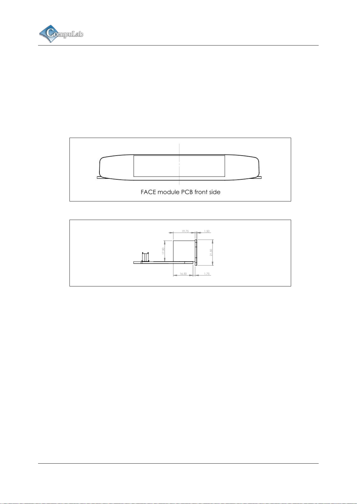
6.2 FACE Module Panel Design
Can be made of sheet metal 1.3mm to 1.4mm
Connector holes can be manufactured by laser cutting, milling or punching.
Full mechanical drawings are available as part of the “FACE module design package” at
http://www.fit-pc.com/.
Figure 3 FACE module panel front view
Figure 4 FACE module panel side view
Revised February 2012 FACE Module Design Guide 17
 Loading...