

Compaq 6000, Compaq PW8000, 299300-006 - Professional - 5100, Professional 5100, Professional 8000 Supplementary Manual
...Page 1

November 1998
......................
.......
..................
........
...........
..........
.........
..................
....................
.......................
.......................
.....................
..........
.....................
Compaq Computer
Corporation
ISSD Technol ogy
Communications
ONTENTS
C
Introducti on
Architectur e Overvi ew
Advanced SMP
Pentium Pro Processor
Pentium II Proces sor
Dual Memor y Buses
Dual-Peer PCI Buses
Multiple Drives
Alternati ve
Architectur es
Typical NT/ X86
Architecture
Unified Memory
Architecture
Crossbar Switc h
Architecture
AGPset Architect ure
Conclusion
1
ECG066/1198
3
3
3
4
4
5
8
8
9
9
9
11
12
13
T
ECHNOLOGY
.
.
.
.
.
Highly Parallel System Architecture for
.
.
.
.
.
.
.
Compaq Professional Workstations
.
.
.
.
.
.
.
5100, 6000, and 8000
.
.
.
.
.
As critical applications for financial analysis, computer-aided design (CAD), computer-
.
.
.
aided engineering (CAE), and digital content creation (DCC) place growing demands on
.
.
.
.
system resources, increasing system bandwidth becomes a critical business issue. After
.
.
.
evaluating available system architectures, Compaq determined that only a new, highly
.
.
.
parall el s ys t em a r ch i t ecture could p r ovide the requ i r ed l evel s o f p er f o r ma n ce, processo r
.
.
.
and I/O expandability, and bandwidth to satisfy the needs of workstation users. Compaq
.
.
.
is therefore implementing a new architecture that delivers the greatest bandwidth
.
.
.
available today for systems running such demanding applications under the Microsoft
.
.
.
.
Windows NT operating system.
.
.
.
.
This technology brief describes the new Highly Parallel System Architecture and
.
.
.
differentiates it from other architectures used in X86 systems.
.
.
.
.
.
.
.
.
.
.
.
.
.
.
.
.
.
.
.
.
.
.
.
.
.
.
.
.
.
.
.
.
.
.
.
.
.
.
.
.
.
.
.
.
.
.
.
.
.
.
.
.
.
.
.
.
.
.
.
.
.
.
.
.
.
.
.
.
.
.
.
.
.
.
.
.
.
.
.
.
.
.
.
.
.
.
.
.
.
.
.
.
Please direct comments regarding this communication to the ISSD Technology Communications Group at this Internet address:
.
.
.
TechCom@compaq.com
.
.
.
.
.
B
RIEF
Page 2

ECG066/1198
ECHNOLOGY BRIEF
T
.
.
.
OTICE
N
.
.
.
.
.
The information in this publication is subject to change without notice and is provided “AS IS”
.
.
.
WITHOUT WARRANTY OF ANY KIND. THE ENTIRE RISK ARISING OUT OF THE USE
.
.
.
OF THIS INFORMATION REMAINS WITH RECIPIENT. IN NO EVENT SHALL COMPAQ
.
.
.
BE LIABLE FOR ANY DIRECT, CONSEQUENTI AL, INC I DE NT AL, SPECIAL, PUNITIVE
.
.
.
OR OTHER DAMAGES WHATSOEVER (INCLUDING WITHOUT LIMITATION,
.
.
DAMAGES FOR LOSS OF BUSINESS PROFITS, BUSINESS INTERRUPTION OR LOSS OF
.
.
.
BUSINESS INFORMATION), EVEN I F COMPAQ HAS BEEN ADVI SE D OF T HE
.
.
.
POSSIBILITY OF SUCH DAMAGES.
.
.
.
.
.
The limited warranties for Compaq products are exclusively set forth in the documentation
.
.
.
accompanying such products. Nothing herein should be construed as constituting a further or
.
.
.
additional warranty.
.
.
.
.
This publication does not constitute an endorsement of the product or products that were tested.
.
.
.
The configuration or configurations tested or described may or may not be the only available
.
.
.
solution. This test is not a determination of product quality or correctness, nor does it ensure
.
.
.
compliance with any federal state or local requirements.
.
.
.
.
Compaq, Contura, Deskpro, Fastar t , Compaq In sight Manager, LTE, PageMar q, Systempro,
.
.
.
Systempro/LT, ProLiant, TwinTray, ROMPaq, LicensePaq, QVision, SLT, ProLinea, SmartStart,
.
.
.
NetFlex, DirectPlus, QuickFind, RemotePaq, BackPaq, TechPaq, SpeedPaq, QuickBack, PaqFax,
.
.
.
Presario, SilentCool, CompaqCare (design), Aero, SmartStation, MiniStation, and PaqRap,
.
.
.
ProSignia, Concerto, Vocalyst, and MediaPilot are registered with the United States Patent and
.
.
.
Tradema rk Office.
.
.
.
.
Change is Good, Compaq Capital, Colinq, Armada, SmartQ, Counselor, CarePaq, Netelligent,
.
.
.
Smart Uplink , Ext ended Repeater A rchitectu re, Scalabl e C lock Archit ecture, QuickChoi ce,
.
.
.
Systempro/XL, Net1, LTE Elite, PageMate, SoftPaq, FirstPaq, SolutionPaq, EasyPoint, EZ Help,
.
.
.
MaxLight, MultiLock, QuickBlank, QuickLock, UltraView, Innovate logo, and Compaq PC Card
.
.
.
Solution logo are trademarks and/or service marks of Compaq Computer Corporation.
.
.
.
.
.
Micr osoft, Windows, Windows NT, Windows NT Advanced Ser ver, SQL Server for Win d ows NT
.
.
.
are trademarks and/or registered trademarks of Microsoft Corporation.
.
.
.
.
NetWare and Novell are registered tra demarks and Intran etWar e, NDS, and Novel l Dir ectory
.
.
.
Services are t rademar k s of Novell, Inc.
.
.
.
.
Pentium is a registered trademark of Intel Corporation.
.
.
.
.
.
Other product names mentioned herein may be trademarks and/or registered trademarks of their
.
.
.
respective companies.
.
.
.
.
©1998 Compaq Computer Corporation. All ri ghts reserved. Printed in the U.S.A.
.
.
.
.
.
.
.
.
.
.
.
.
.
.
Highly Parallel System Architecture for Compaq Professional
.
.
.
.
Workstations 5100, 6000, and 8000
.
.
.
Second Edition (November 1998)
.
.
.
ECG066/1198
.
.
.
.
.
.
.
.
.
.
.
.
.
.
.
2
(cont.)
Page 3

ECG066/1198
ECHNOLOGY BRIEF
T
.
.
.
.
NTRODUCTION
I
.
.
.
.
Achieving greater system bandwidth is a critical issue to businesses running applications for such
.
.
.
demanding tasks as financial analysis, computer-aided design (CAD), computer-aided
.
.
.
engineering (CAE), and digital content creation (DCC). As a technology leader, Compaq
.
.
.
anticipated the growing need for increased bandwidth and pursued possible solutions. As a result
.
.
.
of its R&D efforts, Compaq is one of the first computer companies to implement a unique new
.
.
.
architecture th a t provides the greatest bandwidth possible today for X86 systems runn i ng such
.
.
.
demanding applications under the Microsoft Windows NT operating system. The high bandwidth
.
.
results from a highly parallel system architecture design.
.
.
.
.
.
The Highly Parallel System Architecture consists of parallel processors, parallel memory
.
.
.
controllers, and parallel input/output (I/O). This new architecture is based on high-performance
.
.
.
Intel Pentium Pro and Pentium II processors along with the memory and I/O subsystems that
.
.
.
support them. It in cludes a new standards-based memory architecture tha t provides significantly
.
.
.
greater bandwidth than traditional memory architectures by using dual memory controllers.
.
.
.
These memory controllers independently process memory requests in parallel, thereby effectively
.
.
.
doubling the memory bandwidth of traditional architectures. The new architecture also supports
.
.
dual-peer PCI buses that double I/O bandwidth and allow for more I/O expandability. The new
.
.
.
architecture is being implemented initially in two Compaq products, the Compaq Professional
.
.
.
Workstation 6000 and th e Compaq Professional Workstation 8000.
.
.
.
.
.
This technology brief provides an overview of the new architecture and explains how it differs
.
.
.
from other architectur es used in X86 systems.
.
.
.
.
.
.
.
RCHITECTURE OVERVIEW
A
.
.
.
.
Unli k e any pr evi ou s architectur e u s ed in X8 6 s ystem s , th e new ar chit ectur e bei ng implem ented by
.
.
.
Compaq incorporates a highly parallel system design. As the block diagram in Figure 1
.
.
.
indicates, the new architecture offers parallelism in multiple ways. It supports symmetric
.
.
.
multiprocessing (SMP) with up to four Pentium Pro processors or two Pentium II processors. It
.
.
.
supports dual-peer PCI buses to provide an aggregate PCI bus bandwidth of up to 267 MB/s. It
.
.
.
also features dual memory controllers that deliver a peak aggregate memory bandwidth of 1.07
.
.
.
GB/s.
.
.
.
.
This high degree of hardware parallelism for critical subsystems such as processor, memory, and
.
.
.
I/O maximizes system bandwidth to improve performance in demanding, resource-intensive
.
.
.
applications. Hardware parallelism of this architecture can be increased even more if the system
.
.
.
configuration includes an optional Compaq drive array controller that can increase performance
.
.
.
in d isk-bound ap p lications by accessi ng data in para llel from multiple disk drives.
.
.
.
.
.
.
.
DVANCED
A
.
.
.
.
.
It is widely recognized that SMP has been supported on both RISC/UNIX workstations an d
.
.
.
server s for a n u mber of years. Most peop le do not , however, associate Microsoft Windows NT
.
.
Workstation and the applications that run on it with SMP. Windows NT Workstation does
.
.
.
support SMP; and for runni ng many demanding appl i cations in finance, computer-aided design,
.
.
.
comput er-aided engineeri ng, and d igit al content creat ion, wor k s tati on users can rea p the ben efits
.
.
.
of SMP. Many simulations and analyses performed on workstations in technical computing
.
.
.
environm ents requi re tremen dous nu mbers of calcula tions t hat can t ake h ours or even days to
.
.
.
complete. Fortunately, many of these applications are multi-threaded or otherwise lend
.
.
.
themselves well to multiprocessing. Therefore, a single user of a workstation can take full
.
.
.
advantage of multiple processors.
.
.
.
.
.
.
.
3
(cont.)
SMP
Page 4
ECG066/1198
ECHNOLOGY BRIEF
T
.
.
.
.
.
.
.
.
.
.
.
.
.
.
.
.
.
.
.
.
.
.
.
.
.
.
.
.
.
.
.
.
.
.
.
.
.
.
.
.
.
.
.
.
.
.
.
.
.
.
.
.
.
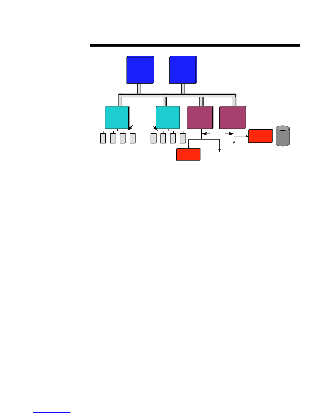
Figure 1. Block diagram of the Highly Parallel System Architecture as implemented in the Compaq
.
.
.
Professional Workstation 6000. This architecture supports up to f our pr ocessors i n the Compaq
.
.
.
Professional Workstation 8000.
.
.
.
.
.
.
The new Highly Parallel System Architecture implemented by Compaq provides excellent
.
.
.
scalability for increased system performance. It supports the use of multiple Intel Pentium Pro
.
.
processors or I ntel Penti um II p rocessors . Each of th es e p rocessors has a dvantages for s p ecific
.
.
.
comput ing environments; therefore, C om p aq is u s ing each of these processors i n n ew product s
.
.
.
being d evel op ed to meet t he widest possible ran ge of customer need s.
.
.
.
.
.
.
.
Pentium Pro Processor
.
.
.
.
The Pentium Pro processor family is Intel's current generation of processors for high-end
.
.
.
desktops, workstations, and servers. This product family consists of processors running at clock
.
.
.
speeds of 150 MHz to 200 MHz with level 2 (L2) memory cache sizes of either 256 KB or 512
.
.
.
KB. The Compaq Professional Workstation 8000 will use the 200-MHz Pentium Pro processor
.
.
.
with an in t egra t ed 512-KB L2 cache that run s at t he core processor speed of 200 MHz. The high-
.
.
.
speed processor and cache provide top performan ce. Because the larger 512-KB L2 cache holds
.
.
.
more instructions, it provides a higher cache hit ra t e th a n the 256-KB cache. The higher cache
.
.
.
hit rate reduces memory bus traffic and therefore increases performance and scalability of the
.
.
.
system.
.
.
.
.
.
.
Pentium II Processor
.
.
.
.
.
The Pentium II processor is the next generation P6 processor from Intel. Formerly code named
.
.
.
Klamath
.
.
versions, each with an int egra t ed 512-KB L2 cache. Compaq is implementing 266-MHz and
.
.
.
300-MHz Pentium II processors in the Compaq Professional Workstation 6000.
.
.
.
.
.
The Pentium II processor provides some enhancements over the Pentium Pro processor, but it also
.
.
.
has some limitations. The Pentium II processor incorporates Intel’s MultiMedia Extensions
.
.
.
(MMX) technology. MMX is the name for 57 multimedia instructions that Intel has added to its
.
.
.
new generation of processors. This instruction set is expected to significantly improve the
.
.
.
performance of processor-intensive multimedia applications that are MMX-aware. MMX is
.
.
tailored to audio, video, and other multimedia tasks. An MMX-equipped workstation will use
.
.
.
only one instruction to execute the same task that a Pentium Pro processor would perform using
.
.
.
.
.
4
Memory
Controller
, the Pentium II processor will be available in 233-MHz, 266-MHz, and 300-MHz
(cont.)
CPU CPU
Processor Bus
(533 MB/s)
Memory
Controller
Memory Bus
(533 MB/s)
Graphics
Controller
PCI
Controller
Controller
PCI Bus
(133 MB/s)
PCI Slots and
other Devices
PCI Slots and
other Devices
PCI
SCSI
Controller
Disk
Page 5

ECG066/1198
Read 128 bits from RAM
Read 128 bits from RAM
64 bits to CPU
64 bits to CPU
64 bits to CPU
64 bits to CPU
Time
ECHNOLOGY BRIEF
T
.
.
up to 16 instructions. Because multimedia operations such as video and audio use a number of
.
.
.
redu ndant i nstructions, M MX achi eves some efficien cies by using a technique called SI MD
.
.
.
(single instruction multiple data). SIMD reduces the required number of clock cycles by
.
.
.
performing redundant instructions on multiple sets of data.
.
.
.
.
For its L2 cache, t he Pen tium I I processor uses industry-stand ard S RAM ( s tatic ra ndom a cces s
.
.
.
memory). This implementation is sometimes referred to as a half-speed cache because the SRAM
.
.
.
runs at hal f t he core p rocessor speed. Use of a half- sp eed L2 cache in s tead of a full-sp eed L2
.
.
.
cache improves manufacturability; however, it increases cache access time, which limits
.
.
.
scalability and performance. Pentium II systems will support a maximum of two processors and
.
.
.
are limited to 512 MB of addressable system memory. The Pentium II processor is capable of
.
.
.
caching 512 MB of system memory. Adding more memory will significantly degrade system
.
.
.
performance because the additional memory will not be cached. Therefore, to ensure application
.
.
.
performance, the Compaq Professional Workstation 6000 will not boot if more than 512 MB of
.
.
.
system memory is installed.
.
.
.
.
.
.
.
UAL MEMORY BUSES
D
.
.
.
.
The new ar chit ecture also includ es two independentl y oper ating memory buses, ea ch r u nning at a
.
.
.
peak speed of 533 MB/s. Together they provide a peak aggregate memory bandwidth of
.
.
.
1.07 GB/s—two to four times the memory bandwidth of other X86/NT workstations. This high
.
.
.
memory bandwidth is the key to delivering the highest performance levels of both single
.
.
.
processor and SMP-aware applications.
.
.
.
.
.
Each memory bus is 144 bits wide and consists of 128 bits of data plus 16 bits for Error Checking
.
.
.
and Correction (EC C ). The new arch itectu re uses buffered 60- ns Ex tended D ata Ou t (EDO )
.
.
.
DIMMs (Dual Inline Memory Modules), and the memory is interleaved. Interleaved memory
.
.
takes advantage of the sequential nature of program execution to overcome delays resulting from
.
.
.
Column Address Strobe (CAS) precharge.
.
.
.
between back - to-back a cces ses to the s ame Dynamic Random Access Memory (DRAM) chip
.
.
.
while the DRAM chip charges back up after a destructive read.
.
.
.
.
.
When interleaved memory is used, banks of DRAM are divided into two or more physically
.
.
.
separate area s . Consecu tive ad d resses a re stored in differ ent a reas of a bank. Th is makes it
.
.
.
possible for the next sequential read to begin on bank B while bank A is precharging from the
.
.
.
previous read, and vice versa. Thus, interleaved memory can significantly increase memory
.
.
throughput for sequential reads.
.
.
.
.
.
EDO memory is capable of tran s ferring d ata every other clock cycle (30 ns for a 60-MHz bus ) .
.
.
.
Non-EDO (Fast Page Mode) memory, on the other hand, is capable of transferring data every four
.
.
.
clocks (60 ns for a 66-MHz bus). With the combination of interleaved memory and EDO
.
.
.
memory, 128 bits of data (plus 16 bits ECC) are read at a time. As Figure 2 illustrates, the first
.
.
.
64 bits of the read go to the processor on one clock pulse, and the second 64 bits of data go on the
.
.
.
next clock pulse. This enables the memory bus to transfer data at the peak data rate of the
.
.
.
processor.
.
.
.
.
.
.
.
.
.
.
.
.
.
.
.
.
.
.
.
.
.
.
.
Figure 2. Interleaved EDO memory reads 128 data bits at a time and transfers data every other clock
.
.
.
cycle.
.
.
.
.
.
5
(cont.)
CAS precharge
is the time a microprocessor must wait
Page 6

ECG066/1198
CAS Precharge
Time
Send Address to RAM
Transfer Data from RAM
A Typical Memory Cycle
Cycle 1: Bank A
Cycle 2: Bank B
Time
Se nd Address to RAM
Transfer Data from RAM
Se nd Address to RAM
Transfer Data from RAM
CAS Prec harge
CAS Prec harge
ECHNOLOGY BRIEF
T
.
.
Because each of the two memory buses in this architecture is capable of returning data to the
.
.
.
processor at the full 533-MB/s speed of the processor bus, it could seem superfluous to have more
.
.
.
memor y bandwidt h than can be sent across the pr ocess or bus. O ne could envisi on the system
.
.
.
looking like a funnel, with the bottleneck being the processor bus. This is not true, however. To
.
.
.
understand why, we must look at how DRAM memory works.
.
.
.
.
Accessing DRAM memory is relatively slow, in part because the DRAM cannot transfer data
.
.
.
continuously. In fact, as Figure 3 illustrates, a typical memory cycle transfers data only about one
.
.
.
third of the time. First, the DRAM must be precharged. Second, the memory address of the data
.
.
.
being sought must be sent to the DRAM. Finally, the DRAM can transfer data.
.
.
.
.
.
.
.
.
.
.
.
.
.
.
.
.
.
.
.
.
.
.
.
Figure 3. Because a DRAM memory cycle has three components, data is transferred only during about one
.
.
third of the cycle.
.
.
.
.
.
.
In som e cases DRAM ca n tran sfer data faster. I f two sequential cycles q uery add resses on the
.
.
.
same DRAM p age, t hen t he ad d ress for the second cycle can be sent d uring data tra nsfer of t he
.
.
.
first cycle (Figure 4). Once continuous data transfer is established on both memory buses as
.
.
.
illustrated in Figure 4, it is possible to achieve a peak aggregate memory bandwidth of 1.07 GB/s.
.
.
.
.
.
.
.
.
.
.
.
.
.
.
.
.
.
.
.
.
.
Figure 4. Basic timeline for sequential reads from the same page of DRAM.
.
.
.
.
.
.
While it is fairly common for a single processor to access consecutive memory locations,
.
.
.
consecut ive cycles in S M P mach ines are rar ely sent t o nearby address es . Individu al processors
.
.
.
typical ly run programs and access data fr om very different areas of system memor y. T hus, if
.
.
processor 1 reads memory at one location and immediately thereafter processor 2 performs a read,
.
.
.
it will usually be to a very different address. For this reason, most memory cycles in SMP
.
.
.
machines look like the one in Figure 3 and transfer data only about one third of the time, yielding
.
.
.
a more typical memory bandwidth of 177.7 MB/s. This is true of all DRAMs and all SMP
.
.
.
machines; it is not unique to the new highly parallel architecture. By adding a second memory
.
.
.
bus, the new architecture actually doubles typical consumption of the processor bandwidth in
.
.
.
SMP machi nes:
.
.
.
.
.
.
.
.
.
To take full advantage of the two memory buses, at least two memory requests must be issued at a
.
.
.
time, one on each memory bus. SMP Pentium Pro processors can issue up to eight cycles at a
.
.
.
time, which increases the likelihood of having cycles run to both memory controllers. Because a
.
.
.
singl e proce s sor can issu e up t o four cycles, th e dua l memory controller can also boos t the
.
.
.
performance of a single proce s sor.
.
.
.
.
Memory may be added to either bus individually and the system will continue to operate correctly.
.
.
.
For peak per forman ce , h oweve r, e qua l am ounts of me mory should be a dded to both buses at the
.
.
.
same time. Because memory is interleaved between the two memory channels by pairs of
.
.
.
DIMMs, best performance results from using the maximum number of DIMMs for a given
.
.
.
6
177.7 MB/s memory bandwi dth x 2 buses = 355 MB/s
(cont.)
RAS Precharge
...
...
Page 7

ECG066/1198
ECHNOLOGY BRIEF
T
.
.
memory size and evenly splitting those DIMMs between the two memory channels. Table 1 is a
.
.
.
DIMM configuration guide for optimizing performance of dual memory buses. The table shows
.
.
.
matched memory sizes on both banks. Other memory configurations are valid.
.
.
.
.
.
.
.
.
.
.
.
.
.
.
.
.
.
.
.
.
.
.
.
.
.
.
.
.
.
.
.
.
.
.
.
.
.
.
.
.
.
.
.
.
.
.
.
.
.
.
.
.
.
.
.
.
.
.
.
.
.
.
.
.
.
.
.
.
.
.
.
.
.
.
.
.
.
.
.
.
.
.
.
.
.
.
.
.
.
.
.
.
.
.
.
.
.
.
.
.
.
.
.
.
.
.
.
.
.
.
.
.
.
.
.
.
.
.
* The degree of performance optimization is indicated by a numerical range. Level 1 represents the best performance. Levels 2,
.
.
.
3, and 4 indicate progressively lower performance.
.
.
.
.
The exact performance increase to be gained by optimizing the memory subsystem is highly
.
.
.
dependent upon the application. Some applications will see less than 1 percent benefit, while
.
.
.
others may see as much as 33 percent. In general, workstation applications with large data sets
.
.
.
(for exa mple, MacNei l Schwen d ler C orporation’s NASTRAN Finite E lemen t Analysis software)
.
.
.
make better use of the dual memory controllers than most PC productivity applications with small
.
.
.
data sets.
.
.
.
.
.
.
.
.
.
7
T
ABLE
(cont.)
1: G
UIDE FOR CONFIG URING DUAL MEMORY BUSES
O
TO
PTIMIZE PERFORMANCE
Memory Size Memory Bus 1
DIMMs
32 MB — 2 x 16 MB 1
64 MB 2 x 16 MB 2 x 16 MB 1
64 MB — 4 x 16 MB 2
64 MB — 2 x 32 MB 3
128 MB 4 x 16 MB 4 x 16 MB 1
128 MB 2 x 32 MB 2 x 32 MB 2
128 MB — 4 x 32 MB 3
128 MB — 2 x 64 MB 4
256 MB 4 x 32 MB 4 x 32 MB 1
256 MB 2 x 64 MB 2 x 64 MB 2
256 MB — 4 x 64 MB 3
256 MB — 2 x 128 MB 4
512 MB 4 x 64 MB 4 x 64 MB 1
512 MB 6 x 64 MB 2 x 64 MB 2
512 MB 8 x 64 MB — 3
512 MB — 4 x 128 MB 4
1 GB 8 x 64 MB 4 x 128 MB 1
1 GB 4 x 128 MB 4 x 128 MB 2
1 GB 8 x 128 MB — 3
1 GB — 4 x 256 MB 4
2 GB 4 x 256 MB 4 x 256 MB 1
2 GB 8 x 256 MB — 2
Memory Bus 2
DIMMs
Optimization
Level *
Page 8

ECG066/1198
ECHNOLOGY BRIEF
T
.
.
Users should also consider tradeoffs in system cost and memory expansion that may result from
.
.
.
optimizing memory performance. In some cases, optimum memory performance can reduce the
.
.
.
amount of availabl e memory expansion. F or instance, a cost-effective a nd perform ance-enhanced
.
.
.
128-MB configuration can be built with eight 16-MB DIMMs. Upgrading such a system to
.
.
.
512 MB, however, would require the addition of 128-MB DIMMs, which currently are not as cost
.
.
.
effective as eight 64-MB DIMMs or a s replacing some of the 16-MB DIMMs with 64-MB
.
.
.
DIMMs.
.
.
.
.
.
.
.
UAL-PEER
D
.
.
.
.
Some workstation applications require large I/O bandwidth. For example, NASTRAN requires
.
.
.
significant amounts of both I/O bandwidth and memory bandwidth. Other examples include
.
.
.
visualization programs that make heavy use of the 3D-graphics controller. Such applications can
.
.
.
take full advantage of the new Highly Parallel System Architecture.
.
.
.
.
.
The new ar chit ecture features two in depend entl y oper ating PCI buses (that is, peer PCI bu s es),
.
.
.
each runn i ng at a peak speed of 133 MB/s. Together they provide a peak aggregate I/O
.
.
.
bandwidth of 267 MB/s.
.
.
.
.
Since each PCI bus runs independently, it is possible to have two PCI bus masters transferring
.
.
.
data simultaneously. In systems with two or more high bandwidth peripherals, optimum
.
.
.
performance can be achieved by splitting these peripherals evenly between the two PCI buses.
.
.
.
.
The new ar chit ecture also includ es an I/O cache th at improves system concurrency, red u ces
.
.
.
latency for many PCI bus master accesses to system memory, and makes more efficient use of the
.
.
.
processor bus. The I/O cache is a temporar y buffer bet ween th e PCI bus and the processor bus. It
.
.
.
is controlled by an I/O cache controll er. When a P C I bu s master req uests data from system
.
.
.
memory, the I/O cache controller automatically reads a full cache line (32 bytes) from system
.
.
.
memory at the processor tran sfer ra t e (533 MB/s) and stores it in t he I/O cache. If the PCI bus
.
.
.
master is reading memory sequentially (which is very typical), subsequent read requests from that
.
.
.
PCI bus m aster can be serviced from the I/O cache rather tha n directl y from system memory.
.
.
.
Likewise, when a PCI bus master writes data, the data is stored in the I/O cache until the cache
.
.
.
conta ins a full cache l ine. Then the I/O ca che controller a cces ses the processor bus and s ends t he
.
.
.
entire ca che li ne to system memory at the processor bus rat e. Th e I /O cache ensu res bett er overa ll
.
.
.
PCI utilization than other implementations, which is important for high-bandwidth peripherals
.
.
.
such as 3D graphics.
.
.
.
.
In addition to doubling the I/O bandwidth, the dual-peer PCI buses can support more PCI slots
.
.
.
than a single PCI bus, providing greater I/O expandability.
.
.
.
.
.
.
.
ULTIPLE DRIVES
M
.
.
.
.
The high level of har d wa re paral lelism provi d ed in t he n ew arch itecture can be enhan ced even
.
.
.
more by adding multiple disk drives to the system. By using more than one disk drive, certain
.
.
.
disk-oriented operations may run faster. For instance, NASTRAN data sets can grow into
.
.
.
multiple gigabytes of data. Since this data cannot fit into physical memory, it is paged to the disk
.
.
.
drive, which is then continuously accessed by the program as it performs its calculations on the
.
.
.
data. To i mpr ove performance, a RAID- 0 d rive a rray can be used to increase d isk performance.
.
.
.
A RAID-0 drive array will access multiple drives as a single logical device, thereby allowing data
.
.
.
to be accessed from two or more drives a t the s ame time. However, RAID-0 does not implement
.
.
.
fault management and prevention features such as mirroring, as other RAID levels do.
.
.
.
.
.
.
.
.
.
.
.
.
.
.
8
(cont.)
PCI B
USES
Page 9

ECG066/1198
ECHNOLOGY BRIEF
T
.
.
LTERNATIVE ARCHITECTURES
A
.
.
.
.
Compaq is implementing this new Highly Parallel System Architecture because other
.
.
.
architectures do not provide equal levels of bandwidth, performance, expansion, and cost
.
.
.
effectiveness.
.
.
.
.
.
.
.
Typical NT/X86 Architecture
.
.
.
.
Most workstations in t he NT/X86 market support two processors to process instructions
.
.
.
concurrently (Figure 5). Overall system bandwidth is limited in such systems, however, because
.
.
.
each processor must com pete with the other for a cces s to subsystems su ch as m emory an d disk.
.
.
.
.
Traditional memory architectures use a single memory controller through which all memory
.
.
.
requests are processed. Depending on implementation, the maximum bandwidth of these memory
.
.
.
subsystems is either 267 MB/s or 533 MB/s. The actual memory throughput will be limited,
.
.
.
however, by the same DRAM constraints identified earlier in the section “Dual Memory Buses.”
.
.
.
.
.
The new memory architecture that Compaq is implementing, on the other hand, employs dual
.
.
.
memory controllers that can process memory requests in parallel. This design allows memory
.
.
.
bandwidth to reach up to 1.07 GB/s—two to four times the bandwidth of other NT/X86 systems.
.
.
Furthermore, with dual -peer PCI buses, high-bandwidth peri pherals can be placed on separate
.
.
.
PCI buses.
.
.
.
.
.
.
.
.
.
.
.
.
.
.
.
.
.
.
.
.
.
.
.
.
.
.
.
.
.
.
.
.
.
.
.
.
.
.
.
.
.
.
.
.
.
.
.
.
.
.
.
.
.
.
.
.
Figure 5. Typical architecture for an X86 computer running Microsoft Windows NT.
.
.
.
.
.
.
.
Unified Memory Architecture
.
.
.
.
.
Silicon Graphics, Inc. touts the Unified Memory Architecture (UMA) used in their O2
.
.
.
workstation. Although UMA provides a cost-effective system, it does so by sacrificing
.
.
.
perfor man ce. With SGI’ s UMA, th e p rocessor and g raphics controller sha re one memory pool
.
.
.
that is connected by a single bus with a peak bandwidth of up to 2.1 GB/s (Figure 6). As noted
.
.
.
earlier in the section “Dual Memory Buses,” the actual memory throughput will be limited by
.
.
.
DRAM const rai nts. Th e gra p hics contr ol ler stores i ts fra me buffer, Z-buffer, and textures in the
.
.
common memory pool. Because the pr ocessor, t he graphics con troller, and the monit or compete
.
.
.
for access to memory, however, this architecture does not deliver as much actual throughput as
.
.
.
the new High ly Para llel System Architectur e. For exampl e, refreshing the m onitor at 85 Hz at a
.
.
.
screen resolution of 1280 x 1024 true color requires that da ta be transferred to the monitor at a
.
.
.
.
.
9
(cont.)
CPU CPU
Memory
Controller
Graphics
Controller
PCI
Controller
PCI Slots and
other Devices
SCSI
Controller
Disk
Page 10

ECG066/1198
ECHNOLOGY BRIEF
T
.
.
rate of 334 MB/s. The large amount of memory bandwidth consumed by monitor refreshing i s
.
.
.
not available to the processor and graphics controller for other tasks. In contrast, all graphics
.
.
.
cards used in Compaq workstations use dual-ported memory that does not take bandwidth from
.
.
.
the g rap hics contr ol ler.
.
.
.
.
.
.
.
.
.
.
.
.
.
.
.
.
.
.
.
.
.
.
.
.
.
.
.
.
.
.
.
.
.
.
.
.
.
.
.
.
.
.
.
.
.
.
Figure 6. Unified Memory Architecture used in the 02 workstation from Silicon Graphics, Inc.
.
.
.
.
.
.
The new ar chit ecture being impl ement ed by Compaq (Fi gure 7 ) allows t he pr ocess or an d graphics
.
.
.
controller to acces s s ep ara te memory pools concurrentl y. Fu rthermore, the E LS A G loria-L 3D
.
.
.
graphics board and the Diamond Fire GL 4000 3D graphics board available with the new
.
.
.
Compaq workstations have their own frame buffer and Z-buffer/texture memory. They do not
.
.
.
rely on a common pool of memory for most data. Since dat a is acces sed on two separa te buses at
.
.
.
the same time, the actual bandwidth is 1.07 GB/s for the memory bus plus the bandwidth of the
.
.
.
graphics controller memory buses.
.
.
.
.
.
.
.
.
.
.
.
.
.
.
.
.
.
.
.
.
.
.
.
.
.
.
.
.
.
.
.
.
.
.
.
.
.
.
.
.
.
.
.
.
.
.
.
.
.
.
.
.
.
.
.
.
.
Figure 7. The new Highly Parallel System Architecture allows the processors and graphics controller to
.
.
.
access two separate memory buses concurrently.
.
.
.
.
.
.
.
.
.
.
.
.
.
.
.
.
10
Memory
Controller
(cont.)
CPU
CPU CPU
Memory
Controller
Graphics
Controller
Monitor
Memory
Controller
Graphics
Controller
PCI
Controller
Controller
PCI Slots and
other Devices
PCI Slots and
other Devices
PCI
Controller
PCI Slots and
other Devices
PCI
SCSI
Controller
Disk
Page 11

ECG066/1198
ECHNOLOGY BRIEF
T
.
.
.
Crossbar Switch Architecture
.
.
.
.
A crossbar switch architecture provides multiple, independent paths to system memory. As
.
.
.
Figure 8 illustrates, individual paths can be established to memory from each processor or I/O
.
.
.
bus. Thus, a crossbar switch can avoid contention of multiple memory requests on a given bus.
.
.
.
This style of crossbar switch is used in the Sun Microsystems Unified Port Architecture (UPA)
.
.
.
and the Compaq TriFlex architectures.
.
.
.
.
.
.
.
.
.
.
.
.
.
.
.
.
.
.
.
.
.
.
.
.
.
.
.
.
.
.
.
.
.
.
.
.
.
.
.
.
.
.
.
.
.
.
.
.
.
Figure 8. Crossbar switch architecture.
.
.
.
.
.
The Sun UPA provides a peak memory bandwidth of 1.2 GB/s in its full implementation. In
.
.
.
other Sun implementations, however, memory bandwidth is half that or less. The actual memory
.
.
.
throughput of a Sun system with UPA architecture will be limited by the same DRAM constraints
.
.
.
identified earlier in the section “Dual Memory Buses.”
.
.
.
.
.
By allowing separate paths to system memory, this style of crossbar switch can improve
.
.
perfor man ce of both I/O t raffic and processor cycles. A crossbar swi tch for a
.
.
.
bus, memory bus, and I/O bus can be implemented cost effectively. However, a crossbar switch is
.
.
.
an expensive solution in a system with several buses. The reason is that all the buses must go into
.
.
.
a single chip tha t ha s su ffi cient p ins for each bus . Th is req u ires a large and exp ensive chip wh en
.
.
.
several buses are implemented in t he crossbar switch. A crossbar switch supporting the pr ocessor
.
.
.
bus, two PCI buses, and two memory buses is not cost effective with today’s silicon technology.
.
.
.
.
.
Compaq chose not to use a crossbar switch because a better architectural solution was possible for
.
.
.
the following reasons. First, the Pentium Pro processor bus is capable of running up to eight
.
.
transactions simultaneously. Since the I/O cycle can be run simultaneously with processor cycles
.
.
.
on the shared processor bus, independent paths to memory are not as critical. Furthermore, the
.
.
.
I/O ca che sig nificant ly reduces t he am ou nt of bandwidt h required by each PC I bus on the
.
.
.
processor bus. Second, having dual-peer PCI buses and two memory buses can produce
.
.
.
significant performance incr eases. Th e new archi tecture usin g dua l-peer PCI buses and dual
.
.
.
memory controllers on a shared processor bus gives better performance than a crossbar switch
.
.
.
with a single memory controller and a single PCI bus. Moreover, the higher performance comes
.
.
.
at a price point well below that of a crossbar switch with dual memory controllers and dual PCI
.
.
.
buses.
.
.
.
.
.
.
.
.
.
.
.
.
.
.
.
.
.
.
.
11
CPU
(cont.)
Crossbar
Switch
Memory
Controller
PCI
Controller
PCI Slots and
other Devices
single
processor
Page 12

ECG066/1198
ECHNOLOGY BRIEF
T
.
.
.
AGPset Architecture
.
.
.
.
The 440LX AGPset (LX chipset) from Intel is designed primar i l y for the commercial desktop and
.
.
.
consumer desktop markets. However, some workstation vendors are deploying the LX chipset in
.
.
.
machines targeted for workstation applications. Key features of the LX architecture include
.
.
.
.
.
.
.
.
.
.
.
.
.
.
.
.
.
.
.
.
.
.
.
.
.
.
.
.
.
.
.
.
.
.
.
.
.
.
.
.
.
.
.
.
.
.
.
.
.
.
.
.
.
.
.
.
.
.
.
.
.
.
.
.
.
.
.
.
.
.
.
.
.
.
.
.
.
.
.
.
.
.
.
.
.
.
.
.
.
.
.
.
.
.
.
.
.
.
.
.
.
.
.
.
.
.
.
.
.
.
.
.
.
.
.
.
.
.
.
.
.
.
.
.
.
.
.
.
.
.
.
.
.
.
.
.
.
.
.
.
.
.
.
.
12
Singl e PCI bus
•
Single memory bus
•
66-MHz SDRAM memory
•
Advan ced graphics por t (AGP) bus for graph ics car ds
•
Support for up to two Intel Pentium II processors
•
Figure 9 illustrates the LX chipset architecture. The microprocessor, memory, and AGP graphics
buses operate with a peak bandwidth of 533 MB/s, while th e peak bandwidth of the PCI bus is
133 MB/s. This contrasts with th e 1.07-GB/s peak memory bandwidth and the 267-MB/s PCI
bus bandwidth of the Highly Parallel System Architecture.
A single memory
controller provides
maximum bandwidth of
533 MB/s.
Controller
Figure 9. Block diagram of the LX architecture.
The Highly Parallel System Architecture supports industry-standard EDO memory arran ged in
2:1 i nterleaved ba nks. The LX architecture uses 66- MHz SD RAM t echn ol og y, wh ich Compaq
projects to be a very short-lived technology, based on imminent microprocessor and system
architecture advancements. Specifically, Compaq expects that 100-MHz SDRAM will be
available as soon as 100-MHz host-bus systems are available—sometime in the first half of 1998.
Since dual-processor LX workstations are not expected to be generally available until sometime
during the fourth quarter 1997, the 66-MHz SDRAM for workstations may have a useful life of
only about four to six months. Large purchases of 66-MHz SDRAM could result in large
obsolescence costs as early as next year, when users migra te to higher performance 100-MHz
SDRAM technology. This can be a significant expense for customers, as most workstation
applications require large memory configurations. The Highly Parallel System Architecture, on
the other hand, uses proven EDO memory technology that is supported by other Compaq
enterprise products. Customers who plan to migrate to 100-MHz SDRAM next year will be able
to protect and fully amortize their investment in EDO memory by redeploying the EDO memory
into other systems, such a s ProLiant servers an d other worksta t ions.
Memory
(cont.)
CPU CPU
AGP
Controller
Graphics
Controller
The AGP bus provides a dedicated pat h
for the graphics contr oller to
communicate with main memory an d
processors. The AGP-to - memory bus
provides bandwid th of 53 3 MB/s.
A single PCI bus provides
133 MB/s bandwidth for
all attached I/O devices
PCI
Controller
PCI Slots and
other Devices
SCSI
Controller
Disk
Page 13

ECG066/1198
ECHNOLOGY BRIEF
T
.
.
The LX chipset supports an early version of AGP graphics. AGP provides a dedicated 66-MHz
.
.
.
PCI bus connection between the graphics card, processor bus, and main memory. Full-AGP
.
.
.
graphics systems a re able to stor e texture and Z-buffer infor mati on into non-cacheable s ystem
.
.
.
memory. Additionally, future versions of AGP will support AGP bus master cycles that will allow
.
.
.
the AGP card to transfer data on both clock-edges, providing a theoretical 533-MB/s graphics
.
.
.
bandwidth. However, operating system support for AGP bus master cycles will not be available
.
.
.
until mid-1998. AGP systems provide a 66-MHz PCI bus connection to the processor, while
.
.
.
Highly Parallel System Architecture systems provide only a 33-MHz connection to the PCI buses.
.
.
.
This incr eases the gra phics bandwidth from 133 MB/s to 267 MB/s in current AGP systems, but
.
.
.
this adva nta g e can be deceiving . As Compaq tes tin g s hows, this i ncr eased bandwidt h rep resen ts
.
.
.
performance improvement of only about a one percent in most graphics-intensive applications.
.
.
.
This very small increase occurs because graphics performance is limited mostly by CPU and
.
.
.
graphics processor capability and only rarely by bus bandwidth. Compaq workstation engineering
.
.
measurements show that the highest-end 3D-graphics cards typically require no more than
.
.
.
20 percent of a PCI bus, with peaks of up to 40 percent. Thus, PCI graphics cards still have
.
.
.
headroom to double performance without saturating the PCI bus. The dual PCI buses in the
.
.
.
Highly Parallel System Architecture in some cases provide more bandwidth than even a full AGP
.
.
.
implementation. For example, in video editing, the dual PCI buses allow the application to
.
.
.
manage three video streams, something that would not be feasible using only a single PCI bus
.
.
.
implementation.
.
.
.
.
.
Compaq Professional Workstations using the Highly Parallel System Architecture support
.
.
industry-standar d PCI-based 2D- and 3D-graphics solutions. In conjunction with dual-peer PCI
.
.
.
buses, the Highly Parallel System Architecture graphics solutions provide highly competitive
.
.
.
performance for workstation applications.
.
.
.
.
.
For a more detailed comparison of the LX chipset and the Highly Parallel System Architecture,
.
.
.
please refer to the technology brief
.
.
.
AGPset in the Workstation Market
.
.
.
.
.
.
.
ONCLUSION
C
.
.
.
.
As business-critical applications become more demanding, the need for more bandwidth becomes
.
.
.
increasingly important to customers. The new Highly Parallel System Architecture provides high
.
.
.
performance and expansion capability plus unpreceden ted levels of bandwidth for X 8 6 systems
.
.
.
running Windows NT and very demanding applications. As the first computer company to
.
.
.
implement this new architecture, Compaq once again demonstrates its technology leadership in
.
.
.
providing innovative computing solutions to meet the needs of all its customers.
.
.
.
.
.
.
.
.
.
.
.
.
.
.
.
.
.
.
.
.
.
.
.
.
.
.
.
.
.
.
.
.
.
.
.
.
.
.
.
.
.
.
.
.
.
.
.
.
.
13
(cont.)
Highly Parallel System Architec t ure vs. the Int el 440LX
, document number ECG049/1097.
 Loading...