

Page 1
MODIFICATION
# No. DATA CONTENTS
#1 2000.6 Alteration of parts supply, as the service division had changed. (P.6-2)
HISTORY
MODEL NAME :P1100
SERVICE MANUAL
PARTS No. : 9-978-656-01
* Blue characters are linking.
#22000.6Addition of CH model. (P.6-3)
Page 2

P1100
SERVICE MANUAL
N.Hemisphere Model
SPECIFICATIONS
Display 21-in 53.3-cm
Type Color, FD Trinitron
Viewable Image Size
(diagonal)
Face Treatment Antireflective and antistatic coating compliant with TCO
Maximum Weight
(Unpacked) 70.4-lb 32.0-kg
Maximum Dimensions
Height 19.9-in 50.6-cm
Depth 19.4-in 49.3-cm
Width 19.8-in 50.4-cm
Maximum Graphics
Resolution 1920 × 1440 at 75Hz Refresh Rate
Aperture Grille Pitch P22, 0.24 mm
Text Mode 720 × 400
Horizontal Frequency 30 to 121 kHz
Vertical Frequency 50 to 160 Hz
Environmental Requirements Temperature
Operating Temperature
Storage Temperature
19.8-in 50.2-cm
1999 requirements
50 to 95
-22 to 140°F
F
°°
5 to 35 C
°
-20 to 60 C
Humidity (Noncondensing)
Operating
Nonoperating
Power Source 90 - 132/195 - 255 VAC, 50-60 Hz
Power Consumption < 160 Watts
Input Terminal Two 15-pin D-type connectors
Color Display Values
Red
Blue
Green
White Point (9300 K)
Gamma: 2.6
*Commission International d’Eclairage, 1931 Standard.
U/C Model
AEP Model
Japan Model
AUS Model
UK Model
Chinese Model
Chassis No. SCC-L22H-A
G1
20 to 80%
10 to 90%
CIE* Chromaticity Coordinates
x (+/- 0.030) y (+/- 0.030)
0.625 0.340
0.155 0.070
0.280 0.605
0.281 0.311
CHASSIS
COLOR GRAPHIC DISPLAY
Page 3
P1100
SAFETY CHECK-OUT
After correcting the original service problem, perform the following safety checks before releasing the set to the customer:
1. Check the area of your repair for unsoldered or poorly-soldered connections. Check the entire board surface for solder
splashes and bridges.
2. Check the interboard wiring to ensure that no wires are
“pinched” or contact high-wattage resistors.
3. Check that all control knobs, shields, covers, ground straps,
and mounting hardware have been replaced. Be absolutely
certain that you have replaced all the insulators.
4. Look for unauthorized replacement parts, particularly transistors, that were installed during a previous repair. Point
them out to the customer and recommend their replacement.
5. Look for parts which, though functioning, show obvious
signs of deterioration. Point them out to the customer and
recommend their replacement.
6. Check the line cords for cracks and abrasion. Recommend
the replacement of any such line cord to the customer.
7. Check the B+ and HV to see if they are specified values.
Make sure your instruments are accurate; be suspicious of
your HV meter if sets always have low HV.
8. Check the antenna terminals, metal trim, “metallized”
knobs, screws, and all other exposed metal parts for AC
Leakage. Check leakage as described below.
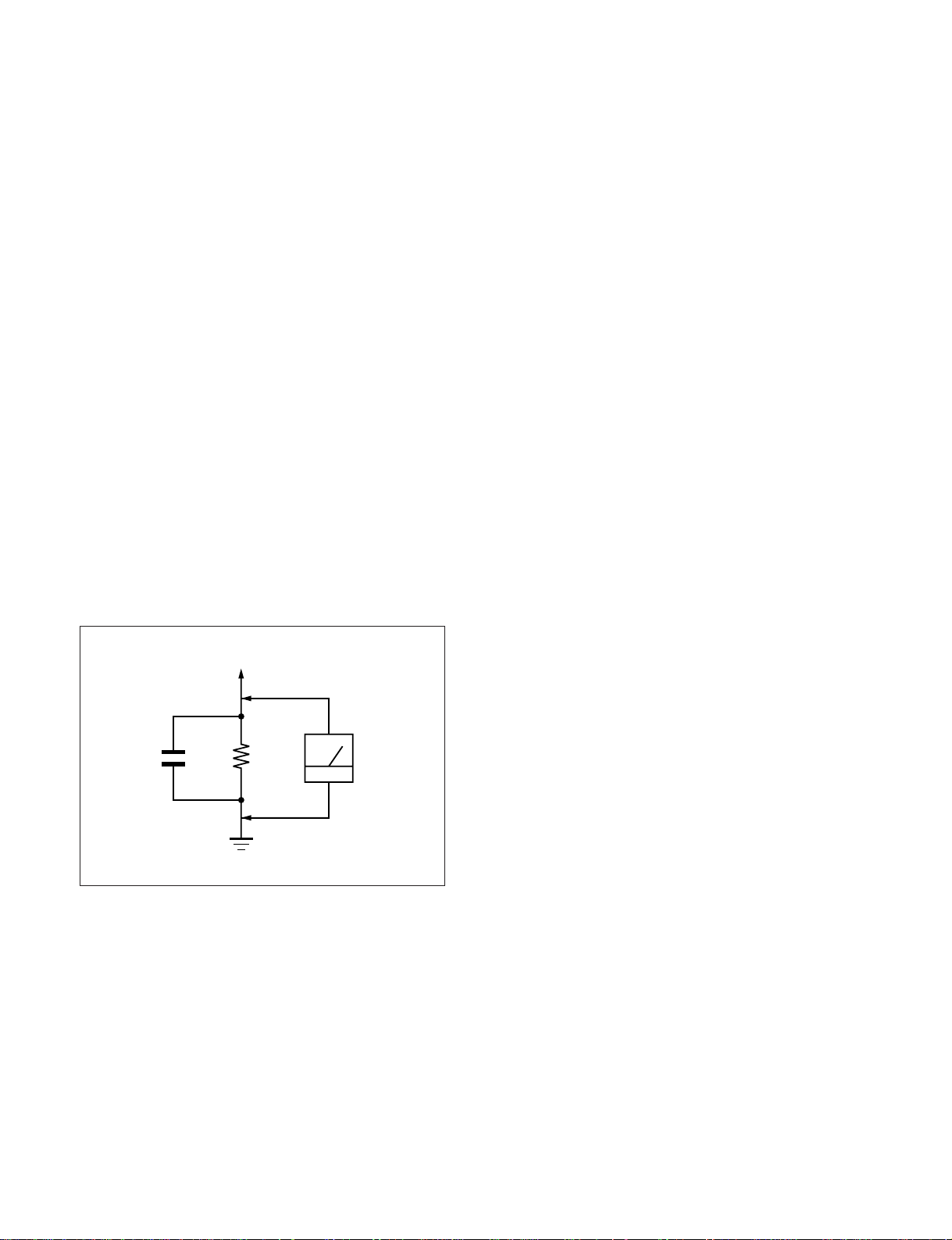
To Exposed Metal
Parts on Set
0.15 µF
1.5 k
Ω
AC
Voltmeter
(0.75 V)
LEAKAGE TEST
The AC leakage from any exposed metal part to earth ground
and from all exposed metal parts to any exposed metal part having a return to chassis, must not exceed 0.5 mA (500 microamperes).
Leakage current can be measured by any one of three methods.
1. A commercial leakage tester, such as the Simpson 229 or
RCA WT-540A. Follow the manufacturers’ instructions to
use these instruments.
2. A battery-operated AC milliammeter. The Data Precision
245 digital multimeter is suitable for this job.
3. Measuring the voltage drop across a resistor by means of a
VOM or battery-operated AC voltmeter. The “limit” indication is 0.75 V, so analog meters must have an accurate lowvoltage scale. The Simpson 250 and Sanwa SH-63Trd are
examples of a passive VOMs that are suitable. Nearly all
battery operated digital multimeters that have a 2 V AC
range are suitable. (See Fig. A)
WARNING!!
NEVER TURN ON THE POWER IN A CONDITION IN
WHICH THE DEGAUSS COIL HAS BEEN REMOVED.
SAFETY-RELATED COMPONENT WARNING!!
COMPONENTS IDENTIFIED BY SHADING AND MARK
¡ ON THE SCHEMATIC DIAGRAMS, EXPLODED
VIEWS AND IN THE PARTS LIST ARE CRITICAL FOR
SAFE OPERATION. REPLACE THESE COMPONENTS
WITH SONY PARTS WHOSE PART NUMBERS APPEAR AS SHOWN IN THIS MANUAL OR IN SUPPLEMENTS PUBLISHED BY SONY. CIRCUIT ADJUSTMENTS THAT ARE CRITICAL FOR SAFE OPERATION
ARE IDENTIFIED IN THIS MANUAL. FOLLOW THESE
PROCEDURES WHENEVER CRITICAL COMPONENTS
ARE REPLACED OR IMPROPER OPERATION IS SUSPECTED.
Earth Ground
Fig. A. Using an AC voltmeter to check AC leakage.
AVERTISSEMENT!!
NE JAMAIS METTRE SOUS TENSION QUAND LA
BOBINE DE DEMAGNETISATION EST ENLEVÉE.
ATTENTION AUX COMPOSANTS RELATIFS À LA
SÉCURITÉ!!
LES COMPOSANTS IDENTIFIÉS PAR UNE TRAME ET
UNE MARQUE
¡ SONT CRITIQUES POUR LA SÉCURITÉ.
NE LES REMPLACER QUE PAR UNE PIÈCE PORTANT LE
NUMÉRO SPECIFIÉ. LES RÉGLAGES DE CIRCUIT DONT
L’IMPORTANCE EST CRITIQUE POUR LA SÉCURITÉ DU
FONCTIONNEMENT SONT IDENTIFIÉS DANS LE
PRÉSENT MANUEL. SUIVRE CES PROCÉDURES LORS
DE CHAQUE REMPLACEMENT DE COMPOSANTS CRITIQUES, OU LORSQU’UN MAUVAIS FONCTIONNEMENT
EST SUSPECTÉ.
– 2 –
Page 4

POWER SAVING FUNCTION
P1100
The energy saver feature has three different modes of operation:
■ Full Power
■ Standby/Suspend
■ Sleep
By selecting settings in the computer's Energy Saver utility, you are
able to determine the length of the inactivity period before the
monitor goes into sleep mode.
The following table describes the monitor energy saver levels
available during the different modes of operation.
Energy Saver Levels*
Mode Power Usage Description
Full Power Less than 145 Watts ON = Normal operation
Standby/Suspend Less than 15 Watts Monitor screen is blank. LED blinks amber
Sleep Approximately 1 Watt Monitor screen is blank. LED turns amber .
Off 0 Watts Monitor screen is blank. LED is OFF. There
Power LED is green.
and green. There is a brief warm-up
period before returning to full power mode.
There is a brief warm-up period before
returning to full power mode.
is a brief warm-up period before returning
to full power mode.
Refer to your computer manual for instructions on setting energy
saver features (sometimes referred to as power management
features).
The energy saver features for monitors only work when
connected to computers that have energy saver features.
DIAGNOSIS
■
Monitor is Working out of Scan Range, Change PC Settings
Indicates the monitor is unable to operate with the selected
input signal. Readjust your video setting to a lower resolution.
■
Monitor in Power Save Mode, Activate Using the PC
Indicates the monitor is in one of the power saving modes.
■
Monitor is Working, Check Signal Cable
Indicates the video cable may not be plugged into the
computer.
If the screen goes blank and the LED is green, remove any video
connections from video connector 1 or 2. You can also turn off the
PC. Press the power switch twice to turn the monitor OFF then ON
again. Press the right arrow button
monitor enters power saving mode. If a color bar pattern appears
then it is likely the problem is not the monitor. Please check the
condition of your computer. If the color bar pattern does not appear,
please inform your service representative of the monitor’s condition.
If the power LED is flashing orange, please make note of the
frequency of flashing and inform your service representative of this
frequency.
(contrast increase) before the
– 3 –
Page 5
P1100
TIMING SPECIFICATION
MODE AT PRODUCTION
RESOLUTION
CLOCK
— HORIZONTAL —
H-FREQ
H. TOTAL
H. BLK
H. FP
H. SYNC
H. BP
H. ACTIV
— VERTICAL —
V. FREQ (HZ)
V. TOTAL
V. BLK
V. FP
V. SYNC
V. BP
V. ACTIV
— SYNC —
INT(G)
EXT (H/V) /POLARITY
EXT (CS) /POLARITY
INT/NON INT
MODE 1 MODE 2 MODE 3 MODE 4 MODE 5 MODE 6 MODE 7 MODE 8 MODE 9
640 X 480 640 X 480 720 X 400 800 X 600 800 X 600 832 X 624 1024 X 768 1024 X 768 1152 X 870
25.175 MHz 36.000 MHz 28.322 MHz 49.500 MHz 56.250 MHz 57.283 MHz 78.750 MHz 94.500 MHz 100.000 MHz
31.469 kHz 43.269 kHz 31.469 kHz 46.875 kHz 53.674 kHz 49.725 kHz 60.023 kHz 68.677 kHz 68.681 kHz
usec usec usec usec usec usec usec usec usec
31.778 23.111 31.777 21.333 18.631 20.111 16.660 14.561 14.560
6.356 5.333 6.355 5.172 4.409 5.586 3.657 3.725 3.040
0.636 1.556 0.636 0.323 0.569 0.559 0.203 0.508 0.320
3.813 1.556 3.813 1.616 1.138 1.117 1.219 1.016 1.280
1.907 2.222 1.907 3.232 2.702 3.910 2.235 2.201 1.440
25.422 17.778 25.422 16.162 14.222 14.524 13.003 10.836 11.520
59.940 Hz 85.008 Hz 70.087 Hz 75.000 Hz 85.061 Hz 74.550 Hz 75.029 Hz 84.997 Hz 75.062 Hz
lines lines lines lines lines lines lines lines lines
525 509 449 625 631 667 800 808 915
45 29 49 25 31 43 32 40 45
10113111113
2 32333333
33 25 34 21 27 39 28 36 39
480 480 400 600 600 624 768 768 870
NO NO NO NO NO NO NO NO NO
YES N/N YES N/N YES N/P YES P/P YES P/P YES N/N YES P/P YES P/P YES N/N
NO NO NO NO NO NO NO NO NO
NON INT NON INT NON INT NON INT NON INT NON INT NON INT NON INT NON INT
MODE AT PRODUCTION
RESOLUTION
CLOCK
— HORIZONTAL —
H-FREQ
H. TOTAL
H. BLK
H. FP
H. SYNC
H. BP
H. ACTIV
— VERTICAL —
V. FREQ (HZ)
V. TOTAL
V. BLK
V. FP
V. SYNC
V. BP
V. ACTIV
— SYNC —
INT(G)
EXT (H/V) /POLARITY
EXT (CS) /POLARITY
INT/NON INT
MODE 10 MODE 11 MODE 12 MODE 13 MODE 14 MODE 15 MODE 16 MODE 17 MODE 18
1280 X 1024 1280 X 1024 1280 X 1024 1600 X 1200 1600 X 1200 1792 X 1344 1792 X 1344 1920 X 1440 1920 X 1440
108.000 MHz 135.000 MHz 157.500 MHz 189.000 MHz 229.500 MHz 204.750 MHz 261.000 MHz 234.000 MHz 297.000 MHz
63.981 kHz 79.976 kHz 91.146 kHz 87.500 kHz 106.250 kHz 83.640 kHz 106.270 kHz 90.000 kHz 112.500 kHz
usec usec usec usec usec usec usec usec usec
15.630 12.504 10.971 11.429 9.412 11.956 9.410 11.111 8.889
3.778 3.022 2.844 2.963 2.440 3.204 2.544 2.906 2.424
0.444 0.119 0.406 0.339 0.279 0.625 0.368 0.547 0.485
1.037 1.067 1.422 1.016 0.837 0.977 0.828 0.889 0.754
2.296 1.837 1.016 1.608 1.325 1.602 1.349 1.470 1.185
11.852 9.481 8.127 8.466 6.972 8.752 6.866 8.205 6.465
60.020 Hz 75.025 Hz 85.024 Hz 70.000 Hz 85.000 Hz 60.000 Hz 74.997 Hz 60.000 Hz 75.000 Hz
lines lines lines lines lines lines lines lines lines
1066 1066 1072 1250 1250 1394 1417 1500 1500
42 42 48 50 50 50 73 60 60
1 11111111
3 33333333
38 38 44 46 46 46 69 56 56
1024 1024 1024 1200 1200 1344 1344 1440 1440
NO NO NO NO NO NO NO NO NO
YES P/P YES P/P YES P/P YES P/P YES P/P YES N/P YES N/P YES N/P YES N/P
NO NO NO NO NO NO NO NO NO
NON INT NON INT NON INT NON INT NON INT NON INT NON INT NON INT NON INT
99.09.06 VER.
– 4 –
Page 6

TABLE OF CONTENTS
Section Title Page
1. GENERAL ................................................................. 1-1
2. DISASSEMBLY
2-1. Cabinet Removal ............................................... 2-1
2-2. D Board Removal .............................................. 2-1
2-3. G Board Removal .............................................. 2-2
2-4. A Board, I/O Terminal Board Assembly
Removal ............................................................. 2-2
2-5. N Board Removal .............................................. 2-3
2-6. Service Position .................................................. 2-3
2-7. Bezel Assembly, H AND H2 Boards Removal . 2-4
2-8. US Board Removal ............................................. 2-4
2-9. Picture Tube Removal ....................................... 2-5
2-10. J Board Removal ............................................... 2-6
2-11. Harness Location ............................................... 2-7
P1100
3. SAFETY RELATED ADJUSTMENT............. 3-1
4. ADJUSTMENTS ..................................................... 4-1
5. DIAGRAMS
5-1. Block Diagrams .................................................. 5-1
5-2. Frame Schematic Diagram ................................. 5-7
5-3. Circuit Boards Location ..................................... 5-9
5-4. Schematic Diagrams and Printed Wiring
Boards ................................................................. 5-9
(1) Schematic Diagram of A Board ........................ 5-11
(2) Schematic Diagrams of H, H2, J Boards .......... 5-17
(3) Schematic Diagram of D Board ........................ 5-19
(4) Schematic Diagrams of N (a, b, c) Board 5-23
(5) Schematic Diagram of G Board ........................ 5-31
(6) Schematic Diagram of US Board ...................... 5-35
5-5. Semiconductors ................................................. 5-38
6. EXPLODED VIEWS
6-1. Chassis ............................................................... 6-1
6-2. Picture Tube ...................................................... 6-2
6-3. Packing Materials ............................................... 6-3
7. ELECTRICAL PARTS LIST ............................ 7-1
Note: Hand degauss
This model has an automatic earth magnetism correction function by using an earth
magnetism sensor and a LCC coil. When using a hand degauss while monitor (LCC
coil) is being operated, it sometimes gets magnetized, and the system may not work
properly as a result.
must be used on stand-by or power-off condition.
– 5 –
Page 7

The operating instructions mentioned here are partial abstracts
English 1-3
Setting Up the Monitor
To set up the monitor, ensure that the power is turned off to the
monitor, computer system, and other attached devices, then follow
these steps:
1. Place the monitor in a convenient, well-ventilated location
near your computer.
2. Connect the monitor signal cable 3 to one of the two 15-pin
connectors 4 on the rear panel of the computer and tighten
the screws.
Be sure the signal cable aligns with the 15-pin connector.
Do not force the cable onto the connector or you may
damage the signal cable.
3. Connect one end of the monitor power cord 1 to the
connector on the back of the monitor and the other end 2 to
an electrical outlet that is easily accessible and close to the
monitor.
4
3
1
2
1-4 English
!
WARNING:
To reduce the risk of electric shock or damage
to your equipment:
■
Do not disable the po wer cord grounding plug. The
grounding plug is an important safety feature.
■
Plug the power cord into a grounded (earthed)
electrical outlet that is easily accessible at all times.
■
Disconnect po wer from the monitor by unplugging
the power cord from the electrical outlet.
■
Do not place an ything on power cords or cables.
Arrange them so that no one may accidentally step on
or trip over them. Do not pull on a cord or cable.
When unplugging from the electrical outlet, grasp the
cord by the plug.
from the Operating Instruction Manual. The page numbers of
the Operating Instruction Manual remain as in the manual.
1-1
SECTION 1
GENERAL
Page 8

English 1-5
Using USB Connectors
The base of the monitor has five Universal Serial Bus (USB)
connectors. Four of these connectors, 1,2,3,and 4, are for
connecting USB compatible devices such as a keyboard, mouse, or
joystick to the hub. USB connector 5 is used to connect the USB
signal cable to the computer. The USB signal cable is included with
the monitor.
The following are required to operate the USB hub:
■ Your computer must be fitted with a USB port.
■ Your computer must have Microsoft Windows 95 OSR2.1 or
later, or Microsoft Windows 98 as the operating system.
2
314
5
1-6 English
Operating the Monitor
Front Panel Controls
No./Icon Control Function
1
Reset Button Pressing this button resets the following items: Contrast,
brightness, size/center, geometry, screen, zoom, and
color. OSD Position, Color Mode, Control Lock, and
Language can not be reset.
2
Auto Adjust Provides automatic horizontal and vertical centering and
sizing.
3
1 2
Input/Select Button Selects either video input 1 or 2.
4
Brightness Button Down arrow Decreases brightness or is used to select
menu adjustment
5
Brightness Button Up arrow Increases brightness or is used to select menu
adjustment.
6
Menu Button Launches on-screen menus and selects the functions.
Also, exits menus and on-screen display.
7
Contrast Button Left arrow decreases contrast or is used to adjust selected
OSD adjustment item.
11
1
2
3 4 5 6 7
8 9 10
1-2
Page 9
English 1-7
Continued
8
Contrast Button Right arrow increases contrast or is used to adjust selected
OSD adjustment item
9
Power Button Turns the monitor on and off.
q;
LED Indicates monitor mode.
1. Green LED indicates monitor is turned on.
2. Alternating Amber/Green LED indicates
Standby/Suspend.
3. Amber LED indicates Sleep Mode.
qa
Light Sensor Automatically adjusts the monitor contrast depending
on the ambient light levels.
1-8 English
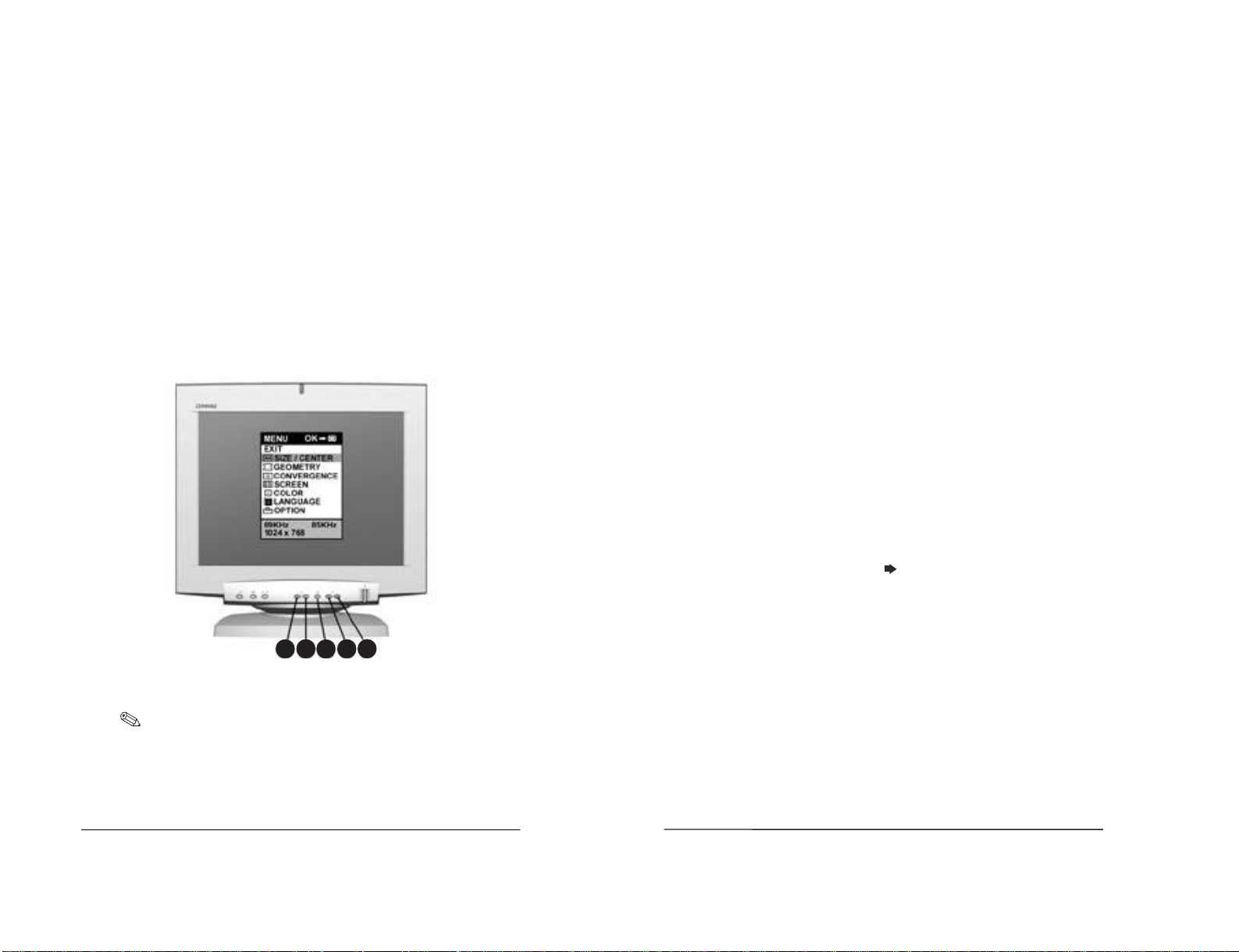
On-Screen Display Settings
To adjust screen settings, press the Menu button 6 to launch the on-
screen display (OSD). The OSD can be viewed in nine available
languages. The following menu shows the functions at each level:
Menu Level 1 Menu Level 2
Size/Center Horizontal Centering
Vertical Centering
Horizontal Sizing
Vertical Sizing
Zoom
Geometry Rotation
Pincushion
Pin Balance
Keystone
Key Balance
Convergence Horizontal Convergence
Vertical Convergence
Vertical Convergence Top
Vertical Convergence Bottom
Screen Landing Left Top
Landing Right Top
Landing Left Bottom
Landing Right Bottom
Moire Cancel
Color Easy - 5000/6500/9300/adjustable
Expert - RGB Gain, RGB Bias
Color Return - optimizes screen brilliance as CRT ages.
Language
English
Francais
Deutsche
OSD Vertical Position
Control Lock
Light Sensor
ModelImformation
* To get this data press the Menu button for 5 seconds while the monitor pricture is stable.
Serial
Manufactured
Espanol
Italiano
Nederlands
(Japanese)
Option Degauss
OSD Horizonal Position
Svenska
(Russian)
1-3
Page 10
English 1-9
How to Adjust Screen Settings
To launch the on-screen display Main Menu:
1. Press the Menu button 3 on the monitor front panel. The
Main Menu will display on the monitor screen.
2. To select an item from the Main Menu, scroll down by
pressing the down arrow button 1 located on the monitor
front panel. To reverse or back up, press the up arrow button
2
.
3. The item to be selected will be highlighted in yellow. Press
the Menu button 3 again.
Monitor with On-Screen Display
The bar on the bottom of the OSD menu shows the
current operating frequency (and resolution if VESA
standard).
234
5
1
1-10 English
4. A second-level menu displays and adjustment scale. Use the
arrow keys 4 or 5 to select a value on the adjustment scale.
5. Press the Menu button 3 to exit from that adjustment.
6. To exit from the on-screen menu, press the Menu button
again.
Press Reset to return the adjustments to their original settings.
Troubleshooting
Special OSD Messages
Special OSD messages will appear on the monitor screen when
identifying the following monitor conditions:
■
Monitor is Working out of Scan Range, Change PC Settings
Indicates the monitor is unable to operate with the selected
input signal. Readjust your video setting to a lower resolution.
■
Monitor in Power Save Mode, Activate Using the PC
Indicates the monitor is in one of the power saving modes.
■
Monitor is Working, Check Signal Cable
Indicates the video cable may not be plugged into the
computer.
Self Diagnosis
If the screen goes blank and the LED is green, remove any video
connections from video connector 1 or 2. You can also turn off the
PC. Press the power switch twice to turn the monitor OFF then ON
again. Press the right arrow button
(contrast increase) before the
monitor enters power saving mode. If a color bar pattern appears
then it is likely the problem is not the monitor. Please check the
condition of your computer. If the color bar pattern does not appear,
please inform your service representative of the monitor’s condition.
If the power LED is flashing orange, please make note of the
frequency of flashing and inform your service representative of this
frequency.
1-4
Page 11
English 1-11
Adjusting Screen Quality
The optimum screen settings are factory preset. However, to change
the settings to your personal preference, allow the monitor to warm
up for 30 minutes before performing the following procedures. The
screen image stabilizes after a warm-up period.
Optimizing Contrast
For best results, set your screen to a light background (such as the
Windows Desktop) before adjusting the following settings:
1. Set the brightness control to its maximum setting, then reduce
the brightness to your preference.
2. Adjust the contrast setting to your preference.
Optimizing Focus
The default image size is preset at the factory. The front panel
controls can be used to increase the screen size beyond the default
setting. However, expanding the screen image beyond the default
settings may degrade the focus at the outer edge of the screen.
To enhance focus, use the lowest brightness and contrast levels that
provide satisfactory results in your viewing environment.
Settings that maximize contrast may not offer optimum focus,
and settings that maximize focus may not offer optimum
contrast.
1-12 English
Display Resolutions
The display resolutions listed below are the most commonly used
modes and are set as factory defaults. This monitor automatically
recognizes these preset modes and they will appear properly sized
and centered on the screen.
Display Resolutions
Preset Modes Resolutions
1. Industr y Standard 640 × 480 at 60 Hz/31.5 kHz
2. VESA 640 × 480 at 85 Hz/43.3 kHz
3. Industr y Standard 720 × 400 at 70 Hz/31.5 kHz
4. VESA 800 × 600 at 75 Hz/46.9 kHz
5. VESA 800 × 600 at 85 Hz/53.7 kHz
6. Macintosh-compatible 832 × 624 at 75 Hz/49.7 kHz
7. VESA 1024 × 768 at 75 Hz/60 kHz
8. VESA 1024 × 768 at 85 Hz/68.7 kHz
9. Macintosh-compatible 1152 × 870 at 75 Hz/68.7 kHz
10. VESA 1280 × 1024 at 60 Hz/63.9 kHz
11. VESA 1280 × 1024 at 75 Hz/79.9 kHz
12. VESA 1280 × 1024 at 85 Hz/91.1 kHz
13. VESA 1600 × 1200 at 70 Hz/87.5 kHz
14. VESA 1600 × 1200 at 85 Hz/106.3 kHz
15. VESA 1792 × 1344 at 60 Hz/83.7 kHz
16. VESA 1792 × 1344 at 75 Hz/106.3 kHz
17. VESA 1920 × 1440 at 60 Hz/90.0 kHz
18. VESA 1920 × 1440 at 75 Hz/112.5 kHz
When "Factory Reset" is selected by pressing the reset button. The
factory reset values will replace user changes that were made for
only the current operating mode.
If the video input signal meets the Generalized Timing
Formula (GTF) the monitor will automatically provide an
optimal screen image.
1-5
Page 12

English 1-13
Maximum Refresh Rates
This monitor is capable of the maximum refresh rates listed in the
following table. However, the video adapter installed in your
computer must also be capable of supporting these refresh rates in
order for them to operate. Most of the new video adapters being
shipped and sold in computers today are capable of supporting these
calculated refresh rates. Certain video adapters may provide different
timing parameters which could result in slightly different maximum
refresh rates.
Maximum Refresh Resolutions
640 × 480 at 160 Hz
800 × 600 at 160 Hz
1024 × 768 at 140 Hz
1280 × 1024 at 110 Hz
1600 × 1200 at 95 Hz
User Modes
The video controller signal may occasionally call for a mode that is
not preset if:
■
You are not using a Compaq standard graphics adapter.
■
You are not using a preset mode.
If this occurs, you may need to readjust the parameters of the
monitor screen by using the on-screen display. User changes can be
made to any or all of these modes and saved in memory. The
monitor automatically stores the new setting, then recognizes the
new mode just as it does a preset mode. In addition to the 18 factory
preset modes, there are fifteen user modes that can be entered and
stored.
1-14 English
Energy Saver Feature
The energy saver feature has three different modes of operation:
■
Full Power
■
Standby/Suspend
■
Sleep
By selecting settings in the computer's Energy Saver utility, you are
able to determine the length of the inactivity period before the
monitor goes into sleep mode.
The following table describes the monitor energy saver levels
available during the different modes of operation.
Energy Saver Levels*
Mode Power Usage Description
Full Power Less than 145 Watts ON = Normal operation
Power LED is green.
Standby/Suspend Less than 15 Watts Monitor screen is blank. LED blinks amber
and green. There is a brief warm-up
period before returning to full power mode.
Sleep Approximately 1 Watt Monitor screen is blank. LED turns amber.
There is a brief warm-up period before
returning to full power mode.
Off 0 Watts Monitor screen is blank. LED is OFF . There
is a brief warm-up period before returning
to full power mode.
Refer to your computer manual for instructions on setting energy
saver features (sometimes referred to as power management
features).
The energy saver features for monitors only work when
connected to computers that have energy saver features.
1-6
Page 13
1-16 English
■ Keep the monitor in a well-ventilated area, away from
excessive light, heat, and moisture.
■ In a two-monitor system, place the monitors as far apart from
each other as possible to lessen interference between them.
■
Do not open the monitor cabinet or attempt to service this
product yourself. Adjust only those controls that are covered
by the operating instructions. If the monitor is not operating
properly or has been dropped or damaged, contact your
Compaq authorized dealer, reseller, or service provider.
Cleaning the Monitor
To clean the monitor, follow these steps:
1. Turn off the monitor and the computer.
2. Dust the monitor by wiping the screen and the cabinet with
a soft, clean cloth.
If the screen requires additional cleaning, use any antistatic CRT
screen cleaner.
CAUTION:
Do not use benzene, thinner, ammonia, or any
volatile substance to clean the monitor screen or cabinet.
These chemicals may damage the monitor.
Shipping the Monitor
Keep the original packing box in a storage area. You may need it
later if you move or ship your monitor.
English 1-15
Care and Maintenance
This section explains how to care for and maintain your Compaq
monitor during normal everyday use.
Protecting the Monitor
To protect your monitor from overheating and other types of
damage, follow these suggestions:
■
Use only a power source and connection appropriate for this
monitor, as indicated on the marking label/back plate.
■
If an extension cord or power strip is used, make sure that the
cord or strip is rated for the product and that the total ampere
ratings of all products plugged into the extension cord or
power strip do not exceed 80% of the extension cord or strip
ampere ratings limit.
■
Do not overload an electrical outlet, power strip, or
convenience receptacle. The overall system load must not
exceed 80% of the branch circuit rating. If power strips are
used, the load should not exceed 80% of the power strip input
rating.
■
Install the monitor near an outlet that you can easily reach.
Disconnect the product by grasping the plug firmly and pulling
it from the outlet. Never disconnect it by pulling the cord.
■
Unplug the monitor from the wall outlet before cleaning. Do
not use liquid cleaners or aerosol cleaners.
■ Slots and openings in the cabinet are provided for ventilation.
These openings must not be blocked or covered. Never push
objects of any kind into cabinet slots or other openings.
■
Do not place plants on top of the monitor. Water or dirt from
the plant may fall into the vents.
■
Do not drop the monitor or place it on an unstable surface.
■
Do not allow anything to rest on the power cord. Do not walk
on the cord.
1-7
Page 14

A-4 Specifications
Specifications
Compaq P1100 Color Monitor
Display 21-in 53.3-cm
Type Color, FD Trinitron
Viewable Image Size
(diagonal)
19.8-in 50.2-cm
Face Treatment Antireflective and antistatic coating compliant with TCO
1999 requirements
Maximum Weight
(Unpacked) 70.4-lb 32.0-kg
Maximum Dimensions
Height 19.9-in 50.6-cm
Depth 19.4-in 49.3-cm
Width 19.8-in 50.4-cm
Maximum Graphics
Resolution 1920 × 1440 at 75Hz Refresh Rate
Aperture Grille Pitch P22, 0.24 mm
Text Mode 720 × 400
Horizontal Frequency 30 to 121 kHz
Vertical Frequency 50 to 160 Hz
Environmental Requirements Temperature
Operating Temperature
Storage Temperature
50 to 95
°
F
-22 to 140°F
5 to 35°C
-20 to 60°C
Humidity (Noncondensing)
Operating
Nonoperating
20 to 80%
10 to 90%
Power Source 90 - 132/195 - 255 VAC, 50-60 Hz
Power Consumption < 160 Watts
Input Terminal Two 15-pin D-type connectors
Color Display Values
CIE* Chromaticity Coordinates
x (+/- 0.030) y (+/- 0.030)
Red
0.625 0.340
Blue
0.155 0.070
Green
0.280 0.605
White Point (9300 K)
0.281 0.311
Gamma: 2.6
*Commission International d’Eclairage, 1931 Standard.
Specifications A-5
Power Cord
If you were not provided with a power cord for your computer, you
should purchase a power cord that is approved for use in your
country.
The power cord must be rated for the product and for the voltage
and current marked on the product’s electrical ratings label. The
voltage and current rating of the cord should be greater than the
voltage and current rating marked on the product. In addition, the
diameter of the wire must be a minimum of ).75 mm or 18AWG.
And the length of the cord must be between 6 feet (1.8 m) and 12
feet (3.6 m). If you have questions about the type of power cord to
use, contact your Compaq authorized service provider.
A power cord should be routed so that it is not likely to be walked
on or pinched by items placed upon it or against it. Particular
attention should be paid to the plug, electrical outlet, and the point
where the cord exits from the product.
2
1-8
Page 15

P1100
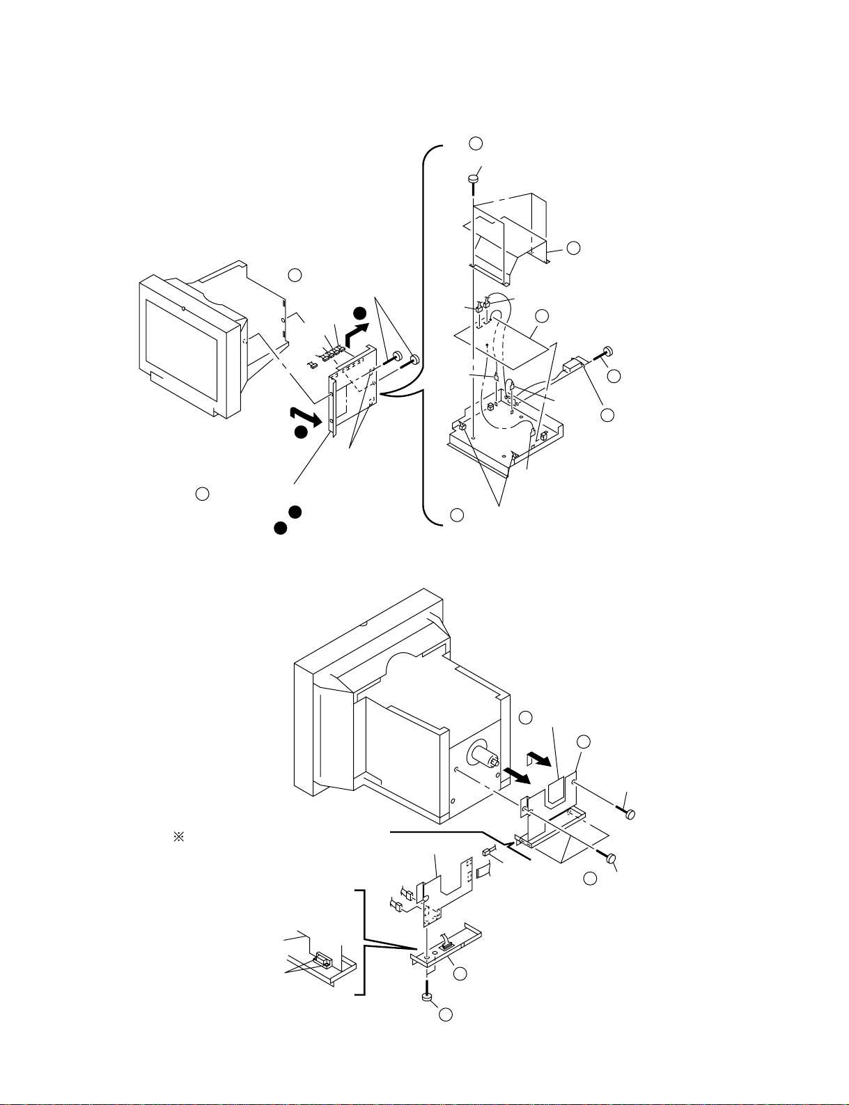
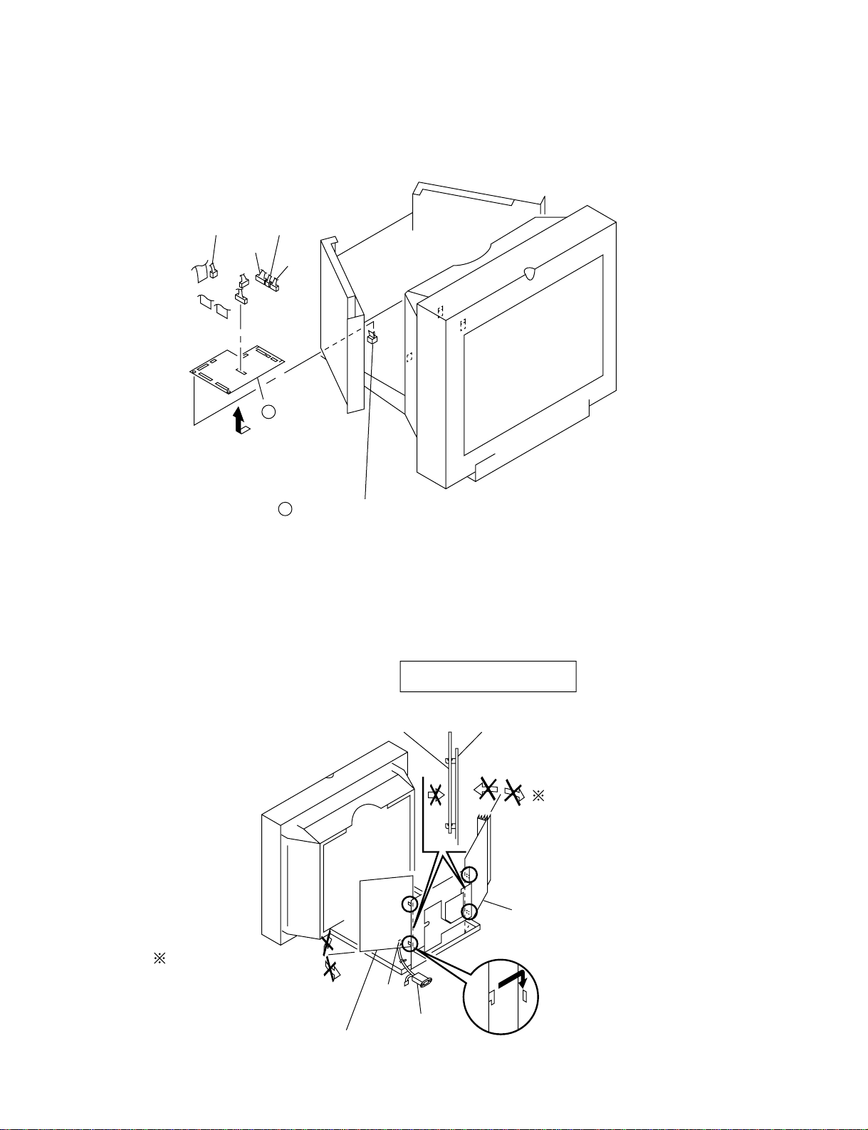
2-1. CABINET REMOVAL
5
4
Four screws
(+ BVTT 4 x 8)
Top cover
SECTION 2
DISASSEMBLY
Push in the tip of a screwdriver
about 5mm to unlock the claw.
Cabinet
Bezel assembly Bezel assembly
3
Cabinet
Cabinet
2
Two claws
1
Two screws
(+ BVTP 4 x 16)
2-2. D BOARD REMOVAL
3 4
Screw
(+ P 3.5 x 20)
5
D board
GND
Two screws
(+ BVTP 3 x 12)
6
7
Video shield
1
Three screws
(+ BVTT 4 x 8)
2
Two claws
Two screws
(+ BVTT 4 x 8)
B
CN504
Two hooks
2
2-1
CN505
A
Open the D block in the direction
of the arrow . and remove of
the arrow .
A
B
Page 16
2-3.G BOARD REMOVAL
CN650
1
Three screws
(+ BVTT 4 x 8)
B
CN654
CN653
CN652
CN651
A
CN601
GND
3
Four screws
(+BVTP 3 x 8)
CN603
6
G board
GND
4
G shield
7
Two screws
(+ BVTP 3 x 8)
8
AC inlet (3P)
P1100
Two hooks
GND
2
Open the G block in the direction
of the arrow . and remove of
the arrow .
A
B
5
Two printed circuit board holders
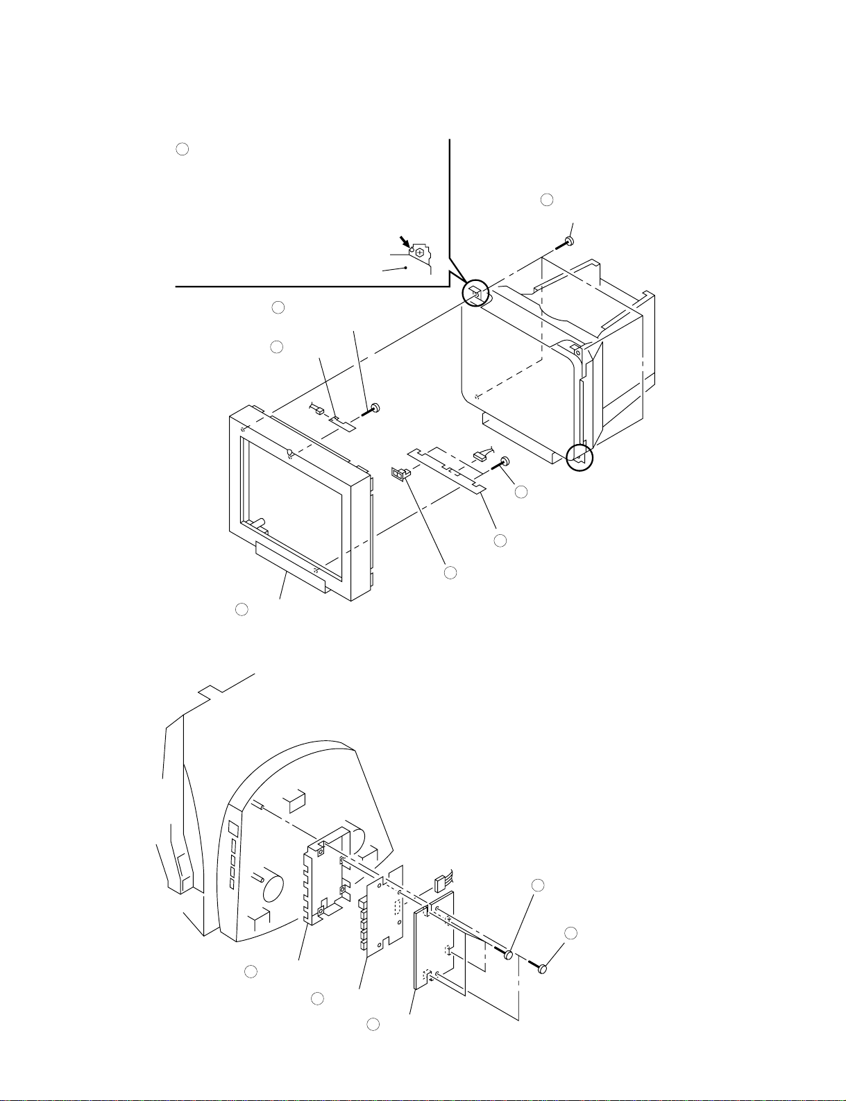
2-4.A BOARD, I/O TERMINAL BOARD ASSEMBLY REMOVAL
3
A board (2/2)
When installing I/O terminal
board assembly, be sure to apply
screw lock on 2 spots after
screws (HD15) are fixed.
A board (1/2)
CN402
CN406
CN403
2
A board (1/2)
Screw (M4)
1
Three screws
(+BVTT 4 x 8)
A board (1/2)
Screw lock
CN405
5
I/O terminal board assembly
4
Two screws
(HD15)
2-2
Page 17
P1100
2-5. N BOARD REMOVAL
CN004
CN001
CN010
CN5002
CN002
CN007
CN011
2-6. SERVICE POSITION
CN5003
CN5001
2
N board
1
Printed circuit board holder
If the claw is hooked,
opening and closing
the board is impossible.
Do not try to do it by force.
G board
(Refer to 2-3.)
D,G boards
CN602
AC inlet (3P)
CAUTION : SHORT
Rear shield
If the claw is hooked,
opening and closing
the board is impossible.
Do not try to do it by force.
D board (Refer to 2-2.)
2-3
Page 18
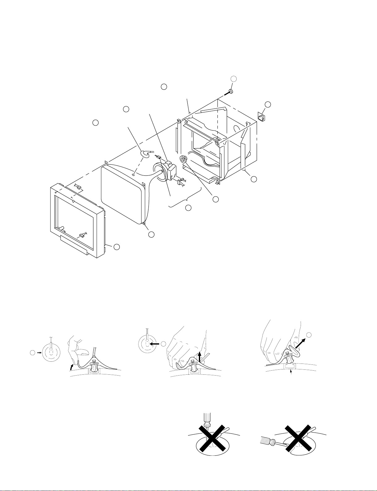
2-7.BEZEL ASSEMBLY, H AND H2 BOARDS REMOVAL
1
Before removing the bezel assembly,
secure the picture tube by attaching two
screws to the picture tube shield at the
positionsshown with an arrow (diagonal
two places) to prevent the picture tube from
falling. (Use the screws +BVTT 4 x 8 that
fix top cover.)
Picture tube shield
7
Screw
(+ BVWHTP 3 x 12)
8
H2 board
CN880
CN801
2
Four screws
(Tapping screw 5)
P1100
3
Bezel assembly
2-8.US BOARD REMOVAL
6
Slide switch cover
CN2601
4
Two screws
(+ BVWHTP 3 x 12)
5
H board
2
Four screws
(+ BVTP 3 x 10)
5
Shield (USB)
4
US board
3
Stand cover
2-4
1
Two screws
(+ BVTP 3 x 10)
Page 19
P1100
2-9. PICTURE TUBE REMOVAL
5
Anode cap
CN880
10
Deflection yoke
1
Open the D block.
(Refer to 2-2.)
CN4
CN5
GND
4
Three connectors
6
Four screws
(Tapping screw 5)
9
Neck assembly
3
A board
2
Open the G block.
(Refer to 2-3.)
CN801
7
Bezel assembly
8
Picture tube
• REMOVAL OF ANODE-CAP
NOTE: Short circuit the anode of the picture tube and the anode cap to the metal chassis, CRT shield or carbon painted on the CRT, after
removing the anode.
• REMOVING PROCEDURES
c
b
a
Anode Button
1 Turn up one side of the rubber cap in
the direction indicated by the arrow a.
2 Using a thumb pull up the rubber cap
firmly in the direction indicated by the
arrow b.
• HOW TO HANDLE AN ANODE-CAP
1 Don’t scratch the surface of anode-caps with shartp shaped
material!
2 Don’t press the rubber hardly not to damage inside of anode-
caps!
A material fitting called as shatter-hook terminal is built in the
rubber.
3 Don’t turn the foot of rubber over hardly!
The shatter-hook terminal will stick out or damage the rubber.
3 When one side of the rubber cap is
separated from the anode button, the
anode-cap can be removed by turning
up the rubber cap and pulling up it in the
direction of the arrow c.
2-5
Page 20
P1100
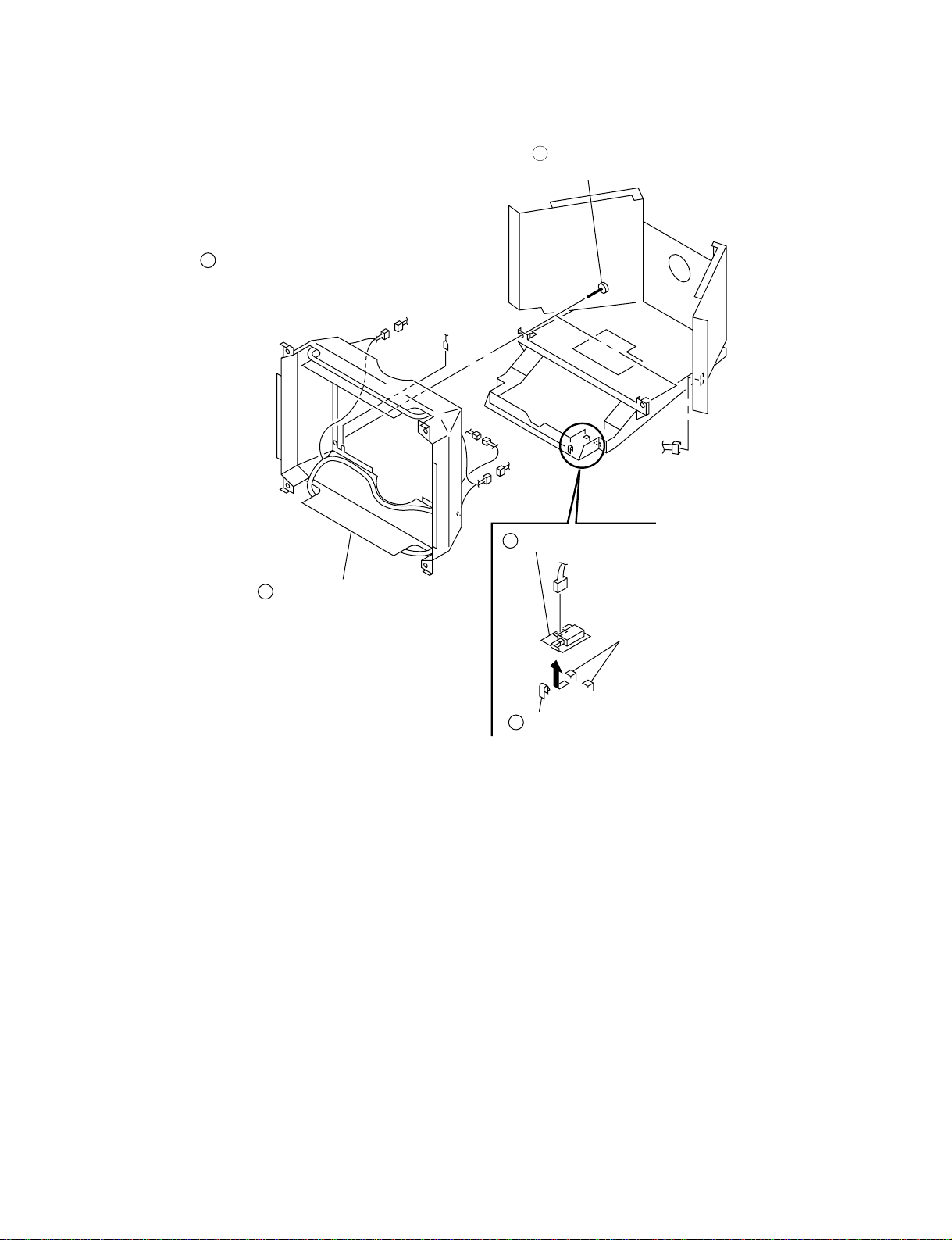
2-10. J BOARD REMOVAL
1
Remove the picture tube.
(Refer to 2-9.)
3
Picture tube shield
complete assembly.
4pin
GND
2pin
4pin
2
Two screws
(+ BVTT 4 x 8)
5
J board
CN601
CN891
Two hooks
4
Claw
2-6
Page 21
P1100
2-11. HARNESS LOCATION
CN651
CN650
CN652
CN653
CN654
US board
CN2601
J board H board
CN601
CN603
CN602
4pin
CN891
CN5001
H2 board
CN5
4pin
CN4
CN5003
CN5002
CN880
CN002
CN801
CN007
CN004
CN001
CN011CN010
Picture tube
4pin
CN505
CN502
CN504
CN501
CN509
CN506
CN508
FBT
G board
AC inlet
N board
CN405
CN402
CN407
D board
Rear shield
I/O terminal board assembly
HD15
CN403CN406
CN408
A board
2-7
Page 22

SECTION 3
SAFETY RELATED ADJUSTMENT
P1100
When replacing or repairing the shown below table, the
following operational checks must be performed as a
safety precaution against X-rays emissions from the unit.
Part Replaced ([)
HV ADJ
HV Regulator
Circuit Check
HV Protector
Circuit Check
Beam Current
Protector Circuit
Check
* Confirm one minute later turning on the power.
a) HV Regulator Circuit Check
1) Enter black crosshatch signal (black on white background), and check that high voltage is in the specified range.
[Specification]: 27.00 ± 0.10 kV
2) Check that the voltage of D912 cathode on the D
board is 27.0 V or more.
b) HV Protector Circuit Check
1) Enter black crosshatch signal (black on white background).
2) Apply the specified voltage to the D912 cathode on
the D board, and check that high voltage is 0.1 kV or
less.
[Specification]: 31.90 + 0.00/– 0.05 V
D Board C920, IC901, R923
D Board C922, C925, C926,
D Board C910, C921, C933,
G Board IC652
N Board IC001, R031, R032
RV901
Part Replaced (])
R924, R929, R945,
RV901, T902(FBT)
• Mounted D Board
D912, D914, D915,
D921, Q907, Q908,
R921, R922, R932,
R937, R939, T902(FBT)
• Mounted D Board
D901, D902, D913,
IC503, IC901, R901,
R920, R928, R930,
R931, R940, R941,
T902(FBT)
• Mounted D Board
• Mounted G Board
• Mounted N Board
c) Beam Current Protector Circuit Check
(1st Protector): D Board
1) Apply 4.5 V DC to CN504 0 pin on the D board,
and check high voltage value.
2) Connect constant current source to a section between
T902 (FBT) qa pin and qs pin (GND) on the D board,
and check that high voltage checked in 1) lowers by
1.50 kV or more when the specified current flows to
the qa pin.
[Specification]: 2.00 + 0.00/– 0.01 mA
d) Beam Current Protector Circuit Check
(2nd Protector): D Board
1) Connect constant current source to a section between
T902 (FBT) qa pin and qs pin (GND) on the D board,
and check that the voltage of CN504 0 pin becomes
0 V or less when the specified current flows to the qa
pin.
[Specification]: 1.70 + 0.00/– 0.01 mA
e) Beam Current Protector Circuit Check
: G Board
1) Apply 264 V AC.
2) Enter about 5 V to CN650 4 pin on the G board, and
check that the output voltage of CN653 2 pin is
about 15 V.
3) Enter about 0 ± 0.2 V to CN654 4 pin, and check
that the output voltage of CN653 2 pin becomes 1.0
V or less.
f) Beam Current Protector Circuit Check
: N Board
1) Check that the protector operates, when the voltage
of CN010 qh pin on the N board is lowered to 0 V or
less (for more than 2 seconds).
3-1
Page 23

P1100
SECTION 4
ADJUSTMENTS
Note: Hand degauss
This model has an automatic earth magnetism correction function by using an earth magnetism sensor
and a LCC coil. When using a hand degauss while monitor (LCC coil) is being operated, it sometimes
gets magnetized, and the system may not work properly as a result.
• Landing Rough Adjustment
1. Enter the full white signal. (or the full black dots signal).
2. Adjust the contrast to the maximum.
3. Make the screen monogreen.
Note: Off the outputs from R ch and B ch of SG.
4. Reverse the DY, and adjust coarsely the purity magnet so
that a green raster positions in the center of screen.
5. Adjust the tilt of DY, and fix lightly with a clamp.
Note: “TILT” = “128”.
• Landing Fine Adjustment
1. Put the set inside the Helmholtz coil. (“LCC SW” = “12”)
2. Input the single green signal and set the “CONTRAST” =
“255”.
Note: After the W/B adjustment with 9300K, measure an aver-
age of ΣIk when a full white signal is entered in the CONT
MAX/BRT CENT status. Then make adjustment so that
the specified screen can be attained after aging for 2 hours
with Ik equivalent to 30% of the average value.
3. Demagnetize the metal part of the chassis with the hand degausser and coil degausser, and the CRT surface with the
hand degausser.
Input AC 230V to AC IN, turn on and off the power to perform auto degaussing. (Perform auto degaussing by setting
“FUNCTION SW” = 1. Return to the original value after
use.)
Demagnetize the CRT surface with the hand degausser
again.
Note:
(1) Hand degauss
tion.
This model has an automatic earth magnetism correction
function by using an earth magnetism sensor and a LCC coil.
When using a hand degauss while monitor (LCC coil) is being operated, it sometimes gets magnetized, and the system
may not work properly as a result.
(2) Adjust in a non-magnetic field.
(3) If adjusting in a magnetic fields, add the shift from the non-
magnetic field in your estimation.
4. Attach the wobbling coil to the designated part of the CRT
neck.
5. Attach the sensor of the landing adjustment unit on the CRT
surface.
must be used on stand-by or power-off condi-
must be used on stand-by or power-off condition.
6. Adjust the DY position and purity, and the DY tilt, and landing of the center and 4 corners with the landing checker.
After adjustment, set “LCC SW” to “13”.
• Write terrestrial magnetism sensor reading VX and VY to
“LCC VX” and LCC VY” respectively. Adjust the landing by moving “LCC NS”, “LCC LT”, “LCC LB”, “LCC
RT” and “LCC RB”. However, the register adjustment
must be limited within the following range.
“LCC NS” 128 ± 15
“LCC LT”, “LCC LB”, “LCC RT”, “LCC RB”
128 ± 40
Save the service data.
<Specifications>
Adjust so that the green is within
the specification given right.
4 corner adjust target : within ± 1
The red and blue must be within
the specification given right with
respect to the green.
A difference between red and blue
must be within the specification
given right.
* Adjustment and measurement should be made at the points
one inch inside the fluorescent screen.
7. For the up/down swing, swing the DY and insert a wedge so
that the up and down pins are equal at the top and bottom.
Adjust the H.TRP VR of DY so that the horizontal trapezoid
is equal at the left and right. Insert the wedge firmly so that
the DY does not shake.
8. Check the landing of each corner, and if it does not satisfy
the specification, adjust the landing of four corners using
“LCC LT“, “LCC LB”, “LCC RT” and “LCC RB”.
However, the register adjustment must be limited within the
following range.
“LCC NS” 128 ± 15
“LCC LT”, “LCC LB”, “LCC RT”, “LCC RB”
After adjustment, save the service data.
9. Remove the sensor and wobbling coil.
10. Switch the signal to R.G.B., and check that each color is
pure.
11. Check that the DY is not tilting, and fix the purity Mg with a
white pen. Fix wedges with RTV.
0 ± 30 ± 7.5 0 ± 3
0 ± 30 ± 7.5 0 ± 3
0 ± 30 ± 7.5 0 ± 3
± 6 ± 6 ± 6
± 6 ± 6 ± 6
± 6 ± 6 ± 6
10 10 10
10 7 10
10 10 10
(µm)
(µm)
(µm)
128 ± 40
4-1
Page 24

P1100
Focus 1
Focus 2
FBT
Connect the communication cable of the computer to the connector located on the D board. Run the service software and then follow
the instruction.
IBM AT Computer
as a Jig
1-690-391-211A-1500-819-A
D-sub
(9 Pin [female])
*The parts above ( ) are necessary for DAS adjustment.
mini Din
(8Pin)
1
2
Interface Unit
3
• Convergence Rough Adjustment
(1) Receive an image of the white crosshatch signals (white
lines on black).
(2) Place the protrusions of the 6-fold poles magnet attached to
the CRT neck upon each other.
(3) Make rough adjustment of the H and V direction conver-
gence by using 4-fold poles magnet.
Purity
4-pole magnet
YCH
H-TRP YBH
6-pole magnet
2-pole magnet
TLH
3-702-691-01
3
Connector Attachment
To BUS CONNECTOR
4 Pin
4 Pin 4 Pin
• White Balance Adjustment Specification
1. 9300K
x = 0.283 ± 0.005
y = 0.298 ± 0.005
(All White)
2. 6500K
x = 0.313 ± 0.005
y = 0.329 ± 0.005
(All White)
3. 5000K
x = 0.346 ± 0.005
y = 0.359 ± 0.005
(All White)
• Vertical and Horizontal Position and Size
Specification
A
b
XBV
APH
XCV
* Set so that the protruding parts of
the 2 magnet rings agree with
each other.
XBVXCV
B
R
TLV
R
B
B
R
R B
• Convergence Specification
V
A
b
a
a
MODE
B
A
B
4 : 3
388
291
5 : 4
364
291
a 2.0 mm
b 2.0 mm
TLH
R
B
YBHYCH
R
R B
BBR
• Focus adjustment
Adjust the focus volume 1 and 2 for the optimum focus.
B
60kHz
fH
0.20 mm
A
0.24 mm
B
60kHz >
0.24 mm
0.28 mm
4-2
Page 25

P1100
MEMO
4-3
Page 26

5-1. BLOCK DIAGRAMS
2345
INPUT2
678910
121113
A
TO N BOARD
CN002
14
15
CONNECTOR PANEL
1
HD15
TO N BOARD
CN001
SECTION 5
DIAGRAMS
CN402
2
BIN2
4
GIN2
6
RIN2
IC401
CN401
HD15
5
15
10
14
4
9
3
13
INPUT1
8
2
12
7
1
11
6
CN403
HOST GND 1
DDC SCL 1
DDC +5V 1
VS1
HS/VS1
DDC SDA 1
INPUT SEL
B
G. SYNC DET
SYNC ON G
CLP
C. BLK
SCL
SDA
H. SYNC
V. SYNC
HFBP
21
19
18
17
16
20
12
7
6
2
4
13
14
8
9
10
(VIDEO AMP, RGB OUT)
A
IC407
5
BIN2
3
GIN2
1
RIN2
11
BIN1
9
GIN1
7
RIN1
18
INPUT SW
14
G. DET
25
SYNC SEP OUT
INPUT SELECT
ROUT
GOUT
BOUT
R DET IN
G DET IN
B DET IN
V-DET
5V
35
32
29
23
21
19
17
VCC KICK
Q402
CLP
C. BLK
SCL
SDA
SCL
SDA
H. SYNC
V. SYNC
HFBP
4
3
5
6
7
IC402
RGB DRIVE
2
RIN
6
GIN
11
BIN
25
D/A5
21
CLP
30
BLK
22
SCL
23
SDA
OSD R
4 9 13 1
18 19 20 21 15 16 17
ROUT
SCL
SDA
VS
Hfly
VDD
OSD G
GOUT
OSD B
BOUT
ROUT
GOUT
BOUT
D/A4
D/A3
D/A2
OSD BLK
8
AV
FBLK
IC404
OSD
41
38
33
26
27
28
PWM2
PWM3
PWM4
PWM1
RCI
GCI
BCI
XT1
XT0
IC403
RGB AMP
12
RIN
8
GIN
2
BIN
15
14
13
26
BUFFER
25
Q101,
Q201,
24
Q301
11
12
RIN
GIN
BIN
ROUT
GOUT
BOUT
X401
8MHz
14
6
4
IC406
CUTOFF AMP
RIK
GIK
12 11 10
BIK
ROUT
GOUT
BOUT
GND
17
IC405 (1/2)
6
–
514
+
3
5
7
DRIFT CORRECT
Q401
7
G2 CONT
Q406, 407, 410
G2
5
3
1
7
CN407
KR
KG
KB
HEATER+
5V-2
+80V
+220V
+12V
5V
CN408
KR
KG
KB
HEATER+
PS401 1A
5
3
1
7
V901
PICTURE TUBE
FVFCHV
CN405
HEATER
9
STBY+5V
1
1W+5V
2
+80V
4
+220V
6
+12V
8
E
TO G BOARD
CN652
CN406
G2
1
C
TO N BOARD
CN010
D
TO N BOARD
CN011
CN504
STBY+5V
RXD
TXD
+15V
+15V
–15V
–15V
HDF
VDF
ABL
HV DET
S0
H CENT
S6
HSPBAL
HLINBAL
H SIZE
H SHAPE
CN505
STBY+5V
1W+5V
ECO SW
PWR SW
DGUS SW
HTR SW
TH DET
S4
S3
S5
S2
S1
HFBP
HD
V RET
VSHAPE
+12V
16
18
20
24
25
22
23
14
12
10
8
7
6
5
4
3
2
1
20
18
16
14
12
10
25
24
23
22
21
19
8
6
3
1
4
HDF
VDF
ABL DET
HV DET
S0
H CENT
S6
HSPBAL
HLIN
H SIZE
HSP
TH DET
S4
S3
S5
S5-1
S2
S1
HFBP
HD
V RET
VSHAPE
2
3
4
2
4
1
6
1
2
3
4
5
6
CN503
STBY+5V
RXD
TXD
CN501
+15V
–15V
+12V
+80V
CN502
STBY+5V
1W+5V
ECO SW
PWR SW
DGUS SW
HTR SW
ECS
TO G BOARD
CN653
F
G
TO G BOARD
CN654
H
TO G BOARD
CN650
+80V
–15V
+15V
+12V
CN508
+220V
+220V
H CENT L
H CENT N
H CENT H
(DEFLECTION)
D
5
4
3
2
1
H CENT
Q514
IC501
PIN CONTROL
HDIN
PWMOUT
ERRIN
H CENT
HSPBAL
+220V
14
3
6
S5
H SENT H
H SENT L
H SENT N
H SENT H
GAIN SW
Q526
5
3
1
2
PIN DRV
Q504, 505
+220V
IC502
H CENT OUT
VCC
VEE
+VIN
OUT
–VIN
PIN OUT
Q508
Q523
S5-1
T501
HDT
+12V
4
7
O2
8
O3
4
H OUT
Q509
Q521, 522
T502
HCT
25
L505
HOC
25
PIN AMP
Q524
–3
391
HSP
H SIZE
ABL
81
H OUT, BUFF
Q515, 520
5
H DRV
Q502, 503
TH DET
T503
HST
21
3
O4
–4
+1
O1
IC503
AMP
ABL DET
TH DET
5
14
13
HFBP
HLIN
IC901
HV CONTROL
14
HDIN
HD
10
ERROUT
12
–
PWMOUT
HVD
11
3
11
+
5
+220V
HV DRV
Q903, 904
ABL
VDF
HDF
V RET
V SHAPE
H DRV
Q701-705
V DRV
Q706, 707
15
14
112
5
7
T701
DFT
3
5
IC701
V DY OUT
OUT VCC
–
HV DET
Q907, 908
+
OUT
+12V
4
2
HV OUT
HV DET
V+
HV REG SW
Q906
V–
23
4
1
T505
HLC
S0-4, S6
HL OUT
Q516, 518
S CAP CHANGE
Q501, 506, 507,
510-513, 517, 525
Q905
1
2
6
5
S5
S5
2
5
RELAY DRV
Q519
T901
HRC
T902 FBT
RY501
HV
17
FC
16
FV
14
15
11
V–
V+
HV ADJ
RV901
CN506
G2
1
HV
FC
FV
CN509
V. DY C
2
V. DY H
3
H. DY H
9
H. DY H
10
H. DY C
5
H. DY C
6
V. DY
R. DY
B-SS9194<U/C> -BD1-EPS05
5-1 5-2
Page 27

µ-COM, V.CONV, H. CONV,
N
LCC, GEO MAGNETIC SENSOR
A
TO CONNECTOR
PANEL
B
TO A BOARD
CN403
C
TO D BOARD
CN504
D
TO D BOARD
CN505
CN002
DDC+5V 2
DDC SCL 2
DDC SDA 2
HS/CS 2
VS 2
HOST GND 2
CN001
DDC+5V 1
DDC SCL 1
DDC SDA 1
HS/CS 1
VS 1
HOST GND 1
CLP
C. BLK
SYNC ON G
INPUT SEL
G. SYNC DET
SCL
SDA
H. SYNC
V. SYNC
HFBP
CN010
ABL
HDF
VDF
HV DET
H CENT
HSPBAL
HLINBAL
HSIZE
HSHAPE
TXD
RXD
+15V
+15V
–15V
–15V
STBY+5V
S0
S6
CN011
S4
S3
S5
S2
S1
TH DET
PWR SW
DGUS SW
HTR SW
VRET
ECO SW
HFBP
HD
VSHAPE
+12V
STBY+5V
1W+5V
DET2
HD SW
Q011
8
VCC
HD DUTY
REG9V
HS
HD
VSHAPE
DET1
VS1
VCLK
IC011
ROM
14
21
CURRENT MILLER
30
15
6
SCL1
SDA1
SCL
SDA
ECO SW
Q001-003
VSPHDHSOUT
Q007
ACTIVE OFF DET
Q004-006
HC1
VC1
+12V
HC2
VC2
VS2
SDA2
SCL2
7
6
5
2
1
4
4
3
2
6
5
1
20
18
16
10
15
9
8
14
13
12
16
12
14
18
20
22
23
24
25
6
8
1
2
3
4
10
19
21
2
3
4
5
7
1
12
14
16
23
10
18
20
25
22
6
8
VS1
SDA1
VS OSD
HFBP
HS2
VC2
SCL1
DET1
HS1
VC1
SOG DET
D SCL
D SDA
HSOUT
+15V
+15V
STBY+5V
ECO SW
HFBP
HD
VSP
+12V
STBY+5V
1W+5V
DET2
Q010
X001
24.756MHz
Q012
IC006
5
6
SDA2
SCL2
48
UBI3
49
UBI4
106
UIN3
107
UIN4
31
P54/INT4
46
UBI1
47
UBI2
104
UIN2
103
UIN1
29
P52/INT2
53
UOUT3
51
UOUT1
108
UIN5
69
P91
41
SCL2
42
SDA2
98
UOUT7
7
75
+
–
15, 94
89
71
128
86
138
126
144
136
133
45
44
54
61
59
58
60
56
55
88
95
93
92
63
64
AIN0
AIN12
DAC0
UPWM8
AIN10
UPWM12
UPWM7
UPWM15
UPWM11
UPWM10
TXD
RXD
PA0
PA6
PA4
PA3
PA5
PA2
PA1
AIN11
P42/D2, P93
P94
P92
INT1
XTB
XTD
IC001
CPU/DSP
UPWM21
UPWM19
UPWM22
UPWM20
UPWM18
UPWM13
UPWM17
UPWM9
P41/D1
P10/A0
P11/A1
P40/D0
P46/D6
P15/A5
AIN7
AIN8
SDA1
SCL1
P82
P90
RESET
AIN1
AIN2
P12/A2
P45/D5
UPWM6
UOUT8
UPWM4
UPWM3
UPWM5
UPWM2
UPWM1
AIN13
P95
UOUT5
UIN6
UOUT4
AIN3
156
152
157
153
149
140
148
131
83
84
39
38
40
33
34
14
3
4
76
13
77
19
8
5
18
124
99
120
117
122
114
111
90
96
67
109
66
78
LED0
LED1
KEYDET
INPUT SW
ENV
5
6
7
VS2
567 8 765
SCL
SDA
VCLK
IC012
ROM
GS5001
GEOSENSOR
IC003
EEP ROM
SDA
SCL
WC
SW
Q008
IC010
H. V. OSC, AFC,
H. DRV, V. SHAPE
VSOSD
HFBP
STBY+5V
VCC
IC002
WDT
3
CK
8
RESET
+15V
25
AFC FIL
35
BSHPLVL
34
DVSHAPE
33
VDC
29
HPHASE
27
HFREQ
13
HPLL
9
AFC SW
5
VSH
8
FBP
4
VSAWRST
1
13
3
11
1
13
3
11
IC5301 (2/2)
6
7
IC5301 (1/2)
4
3
IC5101 (2/2)
6
7
IC5101 (1/2)
4
3
IC5201 (2/2)
6
7
IC5201 (1/2)
4
3
IC5401 (2/2)
6
7
IC5401 (1/2)
4
3
IC004
ECO DET
1CLR
2CLR
1CK
2CK
IC005
ECO DET
1CLR
2CLR
1CK
2CK
8
+
–
2
+
–
+
8
–
+
2
–
+
8
–
2
+
–
8
+
–
2
+
–
CN5002
LCC-LB (+)
3
LCC-LB (–)
4
LCC-LT (+)
1
LCC-LT (–)
2
LCC-RB (+)
7
LCC-RB (–)
8
LCC-RT (+)
5
LCC-RT (–)
6
CN5003
12LCC-NS (+)
LCC-NS (–)
CN5001
ROTATION (+)
5
ROTATION (–)
6
H CONV (+)
3
H CONV (–)
4
V CONV (+)
1
V CONV (–)
2
LCC-LB
LCC-LT
LCC-RB
LCC-RT
LCC-NS
ROTATION
H. CONV
V. CONV
CN007
1W+5V
STBY+5V
LED0
LED1
KEY DET
INPUT SW
ENV
5
1Q
9
2Q
5
1Q
9
2Q
ECO SW
SOG DET
1W+5V
6
STBY+5V
7
LED0
1
LED1
2
KEY DET
3
INPUT SW
4
ENV DRI
8
1 LUMI
CN004
TO H BOARD
I
CN801
TO H2 BOARD
J
CN880
B-SS9194 <U/C> -BD2-EPS05
5-3 5-4
Page 28

I
TO N BOARD
CN007
J
TO N BOARD
CN004
DGC
S891
POWER
J
AC INLET
1W+5V
STBY+5V
LED0
LED1
INPUT SW
KEY DET
ENV DRI
LUMI
CN880
(POWER SW)
CN602
AC L
AC N
CN601
DGC
DGC
CN801
6
7
1
2
4
3
8
H
1
CN891
13AC L OUT
AC L IN
F601
6.3A
1
3
RY603
LED DRV
Q801, 802
LED DRV
Q803, 804
S800
INPUT1INPUT2
S801, S802, S803
RESET ASC V–
S804, S805, S806
MENU H–V+
S807
H+
FUNCTION KEY
1W+5V
STBY+5V
STBY+5V
STBY+5V
1
4
TH801
(USER CONTROL)
AMP
Q881, 882
SW
Q880
POWER
STBY+5V
RELAY DRV
Q691
GR
D801
PHOTO SENSOR
2
CN603
AC L OUT
AC L IN
T601
IC880
3
G
1
3
12
43
(POWER SUPPLY)
TH601
RY602
VCC SW
Q631-633
IC630
8
REG
73
6
REG SW
Q630
2
D610
RECT
3
9
VCC
DRAIN
1
1
2
L410
AFC
VCC SW
Q610
T630
SRT
8
1
2
4
3
5
PH630
3
42
1
3
IC680
3
1
CATHODE
AC SEN
GND
L SEN
5
5
6
REG SW
Q621
IC653
1W+5V REG
1
IN OUT
IC652
STBY+5V REG
2
VCC
IC651
HEATER REG
2
VCC
OUT
CTL
OUT
CTL
VADJ
41
IC650
T620
PIT
3
10
7
T621
PRT
1
2
Q603
REG OUT
START UP
2
4
1
4
1
5
3
4
5
PH620
3
1
PROTECT
2
4
HEATER SW
4
2
1
6
7
Q670
Q671
5
6
7
8
9
10
11
12
PROTECTOR
POWER SW
Q650-654,
667
13AC L OUT
+220V SHUNT REG
D650
D652
PS650
2.0A
CN891
AC L IN
+12V REG
1
IC654
IN OUT
CN2601
6.5V
6.5V
CN2901
V BUS
D–
D+
3
1
2
1
2
3
IC2902
RESET
IC2601
5V-REG
IVCO
5V
CN654
H CENT H
1
H CENT N
2
H CENT L
3
+220V
4
+220V
5
CN653
+80V
6
–15V
4
+12V
1
+15V
2
CN652
+80V
4
+220V
6
+12V
8
HEATER
9
SYBY+5V
1
1W+5V
2
CN650
STBY+5V
1
1W+5V
2
ECO SW
3
HTR SW
6
PWR SW
4
DGUS SW
5
5V
G
41
40
I
G
O
X2901
12MHz
37
25
24
DM0
DP0
RST
XOUT
XIN
TO D BOARD
CN508
TO D BOARD
CN501
TO A BOARD
CN405
TO D BOARD
CN502
IC2901
USB CONT
G
F
E
H
42
DP1
43
DM1
OVR-1
OVR-2
POW-1
POW-2
DM2
DP2
DP3
DM3
OVR-3
OVR-4
POW-3
POW-4
DM4
DP4
31
32
10
POWER SW
Q2601
11
POWER SW
3
2
4
5
35
36
12
13
7
6
Q2602
POWER SW
Q2603
POWER SW
Q2604
IC2602
1
5
15
16
11
12
1
5
15
16
11
12
IC2603
3
7
3
7
(USB CONTROL)
US
B-SS9194 <U/C> -BD3-EPS05
CN2902
3
D+1
2
D–1
1
V BUS1
CN2903
V BUS2
1
C–2
2
D+2
3
CN2904
3
D+3
2
D–3
1
V BUS3
CN2905
1
V BUS4
2
C–4
3
D+4
(PHOTO SENSOR)
H2
5-5 5-6
Page 29

5-2. FRAME SCHEMATIC DIAGRAM
10
CN891
3P
WHT
:VH
POWER
AC L OUT
AC L IN
(POWER SW)
J
INPUT1
CONNECTOR PANEL
12345
678910
11
12131415
HD15D-SUB
INPUT2
123456789
N.C
GND
N.C
+80V
+12V
+220V
1W+5V
9P
WHT
STBY+5V
CN652
:S-MICRO
CN601
4P
WHT
:VH
DGC
1
N.C
2
DGC
1
2
N.C
3
N.C
3
DGC
4
GND
1
1
AC L OUT
2
N.C
3
AC L IN
1
AC L
2
N.C
3
AC N
CN604
1P
CN603
3P
CN602
3P
WHT
:VH
POWER
SUPPLY
4P
WHT
CN651
:S-MICRO
G
6.5V
6.5V
123
HEATER
CN654
8P
WHT
:S-MICRO
H CENT H
1
H CENT N
2
H CENT L
3
+220V
4
+220V
5
N.C
6
GND
7
GND
8
CN653
6P
WHT
:S-MICRO
+12V
1
+15V
2
GND
3
-15V
4
GND
5
+80V
6
CN650
7P
WHT
:S-MICRO
STBY+5V
1
1W+5V
2
ECO SW
3
4
PWR SW
5
DGUS SW
6
HTR SW
7
GND
GND
GND
4
CN401
HD15D-SUB
6789
12345
1112131415
CN402
6P
WHT
:S-MICRO
1
B GND 2
B IN 2
2
G GND 2
3
G IN 2
4
R GND 2
5
R IN 2
6
9P
WHT-L
CN405
8P
WHT
CN002
6P
WHT
CN5001
:S-MICRO
:S-MICRO
:S-MICRO
+220V
N.C
+80V
GND
STBY+5V
1W+5V
123456789
8765432
GND
GND
DDC+5V 2
DDC SCL 2
DDC SDA 2
HOST GND 2
CN5002
ROTATION(+)
ROTATION(-)
V CONV(+)
V CONV(-)
H CONV(+)
H CONV(-)
12345
6
+12V
HEATER
N.C
1
VS2
HS/CS2
8P
YEL
:S-MICRO
LCC-LT(+)
1234567
LCC-LT(-)
LCC-LB(+)
LCC-LB(-)
µ-COM,
V.CONV,H.CONV,LCC,
GEO MAGNETIC SENSOR
LCC-RT(+)
LCC-RT(-)
LCC-RB(+)
LCC-RB(-)
LCC-NS(+)
1
8
A
VIDEO AMP,
RGB OUT
21P
CN403
L-FPC
CLP
GND
ABL(NC)
123456789
21
CLP
GND
21P
:FFC
CN001
ABL(NC)
N
2P
WHT
9P
CN007
:S-MICRO
WHT
:S-MICRO
CN5003
LCC-NS(-)
2
C.BLK
GND
V.SYNC
H.SYNC
SYNC_ON_G
G.SYNC_DET
HFBP
1011121314151617181920
GND
SYNC_ON_G
LED1
KEY_DET
V.SYNC
H.SYNC
G.SYNC_DET
GND
STBY+5V
1W+5V
INPUT_SW
HFBP
ENV_DRI
C.BLK
LED0
123456789
GND
SCL
INPUT_SEL
9
1011121314151617181920
GND
SCL
INPUT_SEL
GND
CN407 CN408
8P 8P
1
KB
2
GND
3
KG
4
GND
5
KR
6
GND
7
HEATER+
8
GND
:VH
G2
1
STBY+5V
GND
N.C
2
CN004
GND
CN010
25P
FFC/FPC
+15V
+15V
-15V
-15V
STBY+5V
HV DET
HCENT
HSPBAL
HLINBAL
HSIZE
HSHAPE
CN011
25P
FFC/FPC
TH DET
STBY+5V
1W+5V
ECO_SW
PWR SW
DGUS SW
HTR SW
HFBP
+12V
VRET
VSHAPE
3P
G2
1
2
3
4
5
GND
6
TXD
7
GND
8
RXD
9
GND
10
11
GND
12
HDF
13
GND
14
VDF
15
GND
16
ABL
17
GND
18
19
S0
20
21
S6
22
23
24
25
1
2
S4
3
S3
4
S5
5
S2
6
7
S1
8
9
GND
10
11
GND
12
13
GND
14
15
GND
16
17
GND
18
19
GND
20
HD
21
GND
22
23
24
GND
25
DDC+5V 1
DDCSCL 1
DDCSDA 1
2345678
DDC+5V 1
DDCSCL 1
DDCSDA 1
CN406
HOSTGND 1
211
HOSTGND 1
LUMI
123
HS/CS 1
VS 1
GND
SDA
SDA
GND
VS 1
HS/CS 1
2P
WHT
KB
1
2
GND
3
KG
4
GND
5
KR
6
GND
7
HEATER+
8
GND
C BLOCK
(CRT SOCKET)
G2
GND
CONNECTOR PANEL GND
2P
WHT
CN506
CN504
25P
:FFC
25
+15V
24
+15V
23
-15V
22
-15V
21
GND
20
TXD
19
GND
18
RXD
17
GND
16
STBY+5V
15
GND
14
HDF
13
GND
12
VDF
11
GND
10
ABL
9
GND
8
HV DET
7
S0
6
HCENT
5
S6
4
HSPBAL
3
HLINBAL
2
HSIZE
1
HSHAPE
CN505
25P
:FFC
25
TH DET
24
S4
23
S3
22
S5
21
S2
20
STBY+5V
19
S1
18
1W+5V
17
GND
16
ECO_SW
15
GND
14
PWR SW
13
GND
12
DGUS SW
11
GND
10
HTR SW
9
GND
8
HFBP
7
GND
6
HD
5
GND
4
+12V
3
VRET
2
GND
1
VSHAPE
8P
WHT
CN508
H CENT H
H CENT N
H CENT L
:S-MICRO
1234567
:VH
+220V
2
N.C
+220V
RCV
H
KB
KR
KG
G1
FV
FC
1
G2
(DEFLECTION)
6P
WHT
CN501
GND
N.C
GND
8
+15V
+12V
:S-MICRO
12345
G2
GM
D
GND
G4
-15V
GND
PICTURE
TUBE
HV
FBT
7P
WHT
CN502
+80V
6
HV
STBY+5V
1W+5V
ECO SW
:S-MICRO
1234567
FV
FC
CN507
1P
GND
1
CN509
10P
:VH
GND
1
V.DY C
2
V.DY H
3
NC
4
H.DY C
5
H.DY C
6
NC
7
NC
8
9
H.DY H
10
H.DY H
CN503
4P
WHT
GND
1
STBY+5V
2
RXD
3
TXD
4
HTR SW
GND
PWR SW
DGUS SW
B-SS9194<U/C>-KESSENZU-EPS05
CHASSIS GND
H.DY
ECS
V.DY
FASTEN
54321
GND
GND
GND
6.5V
6.5V
5P
CN2601
(USB CONTROL)
US
CRT
10
GND
GND
11
GND
CN801
11P
WHT-L
:S-MICRO
SHIELD
123
LUMI
GND
STBY+5V
(PHOTO SENSOR)
CN880
3P
:S-MICRO
H2
V.CONV
H.CONV
ROTATION
LCC-LT
LCC-LB
LCC-RT
LCC-RB
LCC-NS
123456789
GND
LED0
LED1
1W+5V
STBY+5V
KEY_DET
ENV_DRI
INPUT_SW
(USER CONTROL)
H
5-7 5-8
Page 30

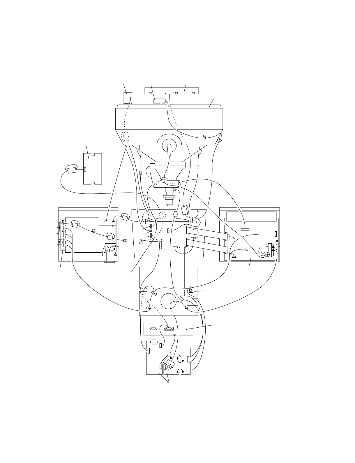
5-3. CIRCUIT BOARDS LOCATION
H2
D
N
H
J
A
US
5-4. SCHEMATIC DIAGRAMS AND PRINTED
WIRING BOARDS
Note:
• All capacitors are in µF unless otherwise noted. (pF: µµF)
Capacitors without voltage indication are all 50 V.
• Indication of resistance, which does not have one for rating
electrical power, is as follows.
Pitch: 5 mm
Rating electrical power 1/4 W (CHIP : 1/10 W)
• All resistors are in ohms.
f : nonflammable resistor.
•
• Ï : fusible resistor.
f : internal component.
•
p : panel designation, and adjustment for repair.
•
• All variable and adjustable resistors have characteristic curve B,
G
unless otherwise noted.
e : earth-ground.
•
• E : earth-chassis.
• The components identified by
have been carefully factory-selected for each set in order to
satisfy regulations regarding X-ray radiation.
Should replacement be required, replace only with the value
originally used.
• When replacing components identified by
necessary adjustments indicated. (See page 3-1)
• When replacing the part in below table, be sure to perform the
related adjustment.
[ in this basic schematic diagram
], make the
HV ADJ
HV Regulator
Circuit Check
HV Protector
Circuit Check
Beam Current
Protector Circuit
Check
D Board C920, IC901, R923
D Board C922, C925, C926,
D Board C910, C921, C933,
Part Replaced ([)
RV901
Part Replaced (])
R924, R929, R945,
RV901, T902(FBT)
• Mounted D Board
D912, D914, D915,
D921, Q907, Q908,
R921, R922, R932,
R937, R939, T902(FBT)
• Mounted D Board
D901, D902, D913,
IC503, IC901, R901,
R920, R928, R930,
R931, R940, R941,
T902(FBT)
• Mounted D Board
G Board IC652
Note: The components identified by shading and
mark ¡ are critical for safety. Replace only
with part number specified.
Note: Les composants identifiés par un tramé et
une marque ¡ sont critiques pour la
sécurité. Ne les remplacer que par une pièce
portant le numéro spécifié.
• All voltages are in V.
• Readings are taken with a 10 MΩ digital multimeter.
• Readings are taken with a color-bar signal input.
• Voltage variations may be noted due to normal production
tolerances.
•
• Circled numbers are waveform references.
•
•
: Can not be measured.
*
s : B + bus.
S : B – bus.
N Board IC001, R031, R032
• Mounted G Board
• Mounted N Board
Terminal name of semiconductors in silk screen
printed circuit ( )
Device Printed symbol Terminal name
Transistor
1
Transistor
2
3
Diode
4
Diode
Diode
5
Diode
6
Diode
7
8
Diode
Diode
9
Diode
0
Diode
qa
Diode
qs
Transistor
qd
(FET)
Transistor
qf
(FET)
Transistor
qg
(FET)
Transistor
qh
Discrete semiconductot
–
(Chip semiconductors that are not actually used are included.)
*
Collector
Base
Collector
Base
Cathode
Cathode
Anode
Cathode
Anode
Common
Anode
Common
Anode Cathode
Common
Anode
Common
Anode Anode
Common
Cathode
Common
Cathode
Anode
Anode
Cathode
Drain
Drain
Emitter
Emitter
Anode
(NC)
(NC)
Cathode
Anode
Cathode
Cathode
Cathode
Anode
Anode
Source
Gate
Source
Gate
Source
Drain
Gate
Emitter
Collector
Base
Circuit
D
G
D
S
D
G
S
S
D
G
G
S
Ver.1.5
• Divided circuit diagram
One sheet of N board circuit diagram is divided into three sheets,
each having the code N-a to N-c. For example, the destination
ab1 on the code N-a sheet is connected to ab1 on the N-b sheet.
a b 1
Ref. No.
Circuit diagram division code
5-9 5-10
Page 31

(1) Schematic Diagram of A Board
A
B
C
D
E
F
G
H
I
123456
CN402
6P
WHT
:S-MICRO
R IN 2
R GND 2
G IN 2
G GND 2
B IN 2
B GND 2
TO CONNECTOR
PANEL
INPUT2
CN401
HD15D-SUB
INPUT1
(HD15)
CN403
21P
L-FPC
ABL(NC)
C.BLK
SYNC_ON_G
G.SYNC_DET
H.SYNC
V.SYNC
INPUT_SEL
HS/CS 1
DDC+5V 1
DDCSCL 1
DDCSDA 1
HOSTGND 1
TO N-a BOARD
CN001
15
14
13
12
11
CLP
GND
GND
HFBP
GND
SCL
SDA
GND
VS 1
10
9
8
7
6
R
R101
6
75
:RN
5
G
4
R201
3
2
1
B
5
4
3
2
1
1
R420
100 :CHIP
2
3
4
5
6
R424
1k :CHIP
7
R428
100 :CHIP
8
R427
1k :CHIP
9
10
11
12
R443
100 :CHIP
13
R444
100 :CHIP
14
15
R445
100 :CHIP
16
R446
100 :CHIP
17
18
47 :CHIP
19
47 :CHIP
20
100 :CHIP
21
D406
1PS226-115
5V
C449
1
10V
B:CHIP
R441
1M
:CHIP
C101
0.01
B:CHIP
R105
47
:CHIP
C201
C102
0.01
47
B:CHIP
R205
25V
47
:CHIP
C202
75
C301
47
:RN
25V
0.01
B:CHIP
R301
C302
75
47
:RN
25V
B:CHIP
R103
R421
100
:CHIP
R422
100
:CHIP
R425
1k
:CHIP
R447
R448
R456
D407
1PS226-115
Q402
2SJ360-TE12L
VCC KICK
S
R406
100k
:CHIP
D402
MA151WK-TX
5V-2
1PS226-115
R305
47
:CHIP
C103
0.01
R
C104
47
75
25V
:RN
G
R203
75
:RN
B
R430
100
:CHIP
R412
220k
:CHIP
C450
0.47
16V
B:CHIP
D101
D201
1PS226-115
1PS226-115
R106
47
:CHIP
C203
0.01
B:CHIP
R206
47
:CHIP
C303
C204
0.01
47
B:CHIP
25V
R303
C304
75
47
:RN
25V
:CHIP
C405
0.1
25V
B:CHIP
SN74HC04ANSR
G SYNC BUFFER
0.6
0.5
L403
100µH
D301
C401
10
D102
1PS226-115
R306
47
:CHIP
5V
R431
470k
IC407
1234567
A1
Y1
A2
Y2
A3
Y3
GND
5V
5V
CH:CHIP
C446
47
25V
123
X401
8MHz
C205
0.01
B:CHIP
C402
47
25V
D202
1PS226-115
D302
1PS226-115
C403
220p
CH:CHIP
R413
100k :CHIP
C404
220p
CH:CHIP
5V-2
C408
0.01
B:CHIP
C413
0.01
B:CHIP
VDD
A6
Y6
A5
Y5
A4
8 9 10 11 12 13 14
Y4
C431
1000p
B:CHIP
R411
4.7k
:CHIP
R438
4.7k
:CHIP
C427
22p
C426
100p
CH:CHIP
C432
0.22 16V
B:CHIP
R419
220
:CHIP
M52757FP-TP
5V
INPUT SELECT
123456789101112131415161718
R_IN2
2.4
VCC2
2.5
G_IN2
VCC2
2.6
B_IN2
VCC2
2.4
R_IN1
GND
2.5
G_IN1
GND
B_IN1
HOLD_CR1
HOLD_CR2
4.3
G.DET
VCC1
V_DET_C
3.4
V_DET
4.5 2.7
INPUT_SW
5V
C406
0.01
B:CHIP
R436
2.2k
:CHIP
4.9
4.9
0.5
0.3
0.7
C425
100p
CH:CHIP
3.4
R417
2.3
1M
:CHIP
3.5
R455
100k
:CHIP
IC401
VCC2
R_OUT
GND
VCC2
G_OUT
GND
VCC2
B_OUT
GND
G_BUF.OUT
G_BUF.IN
0.6
SYNC_SEP.OUT
VCC2
2.7
R_DET_IN
GND
2.6
G_DET_IN
VCC2
B_DET_IN
IC404
CXD9514M
OSD
1234567891011121314
Filter
AGND
SDA
SCL
HS
VS
Hfly
AV
DVDD
DVSS
10
XT1
XT0
PWM0
5V
19 20 21 22 23 24 25 26 27 28 29 30 31 32 33 34 35 36
OSCREF
ADCREF
RCI
GCI
BCI
AVDD
OVDD
FBLK
BOUT
GOUT
ROUT
PWM4
PWM3
PWM2PWM1
5V
C107
0.1
25V
B:CHIP
C216
0.01
B:CHIP
C206
10V
B:CHIP
R202
100k
:CHIP
R402
:CHIP
1
C407
0.01
B:CHIP
1k
C416
2.2
4.3
4.3
4.3
C415
16V
0
0
0
0
R119
15k :CHIP
R219
15k :CHIP
R319
15k :CHIP
15 16 17 18 19 20 21 22 23 24 25 26 27 28
C207
0.1
25V
B:CHIP
C307
0.1
25V
B:CHIP
R261
470
:CHIP
R161
470
:CHIP
C438
0.1
B:CHIP
0.22
B:CHIP
+5V
C112
0.22
16V
B:CHIP
C212
0.22
16V
B:CHIP
C312
0.22
16V
B:CHIP
5V
C410
0.01
B:CHIP
R415
100k
:CHIP
R426
220k
:CHIP
R439
470
:CHIP
R361
470
:CHIP
0.01 B:CHIP
M52749FP-TP
123456789101112131415161718192021
OSD_BLK
0
R_IN
2.7
VCC1(R)
0
OSD_R
GND1(R)
2.6
G_IN
SOG_IN
VCC1(G)
0
OSD_G
GND1(G)
2.72.6
B-IN
VCC1(B)
0
OSD_B
GND
NC
GND1(B)
2.9
ABL_IN
NC
VCC_5V
SOG_OUT
0.1
CLP
C441
C430
0.01
B:CHIP
+12V
IC402
RGB DRIVE
VCC2
2.7
R_OUT
NC
GND2
2.6
G_OUT
NC
GND
4.6
CONT_REF
2.0
Main_Brightness
2.6
B_OUT
GND
4.4
CONT_DAC
0.7
BLK
2.8
D/A_1
D/A_2
D/A_3
D/A_4
D/A_5
GND
4.9
SDA
4.9
SCL
L404
100µH
C423
47
25V
+5V
22 23 24 25 26 27 28 29 30 31 32 33 34 35 36 37 38 39 40 41 42
R_IK
G_IK
B_IK
R_BKG
G_BKG
B_BKG
G2
C443
0.01
B:CHIP
R488
47k
:CHIP
C409
2.2
R491
4.7k
:CHIP
R491
4.7k
:CHIP
C411
220
16V
R107
680
:CHIP
R207
680
:CHIP
C414
22
0.22
B:CHIP
C422
0.22
:CHIP
16V
B:CHIP
R407
:RN-CP
470k
R403
22k
:CHIP
R310
100k :CHIP
R210
100k :CHIP
R110
100k :CHIP
5V
R490
4.7k
:CHIP
C420
16V
R307
680
12V
7
12V
R338
47
:CHIP
R337
470
R313
R316
47
4.7k
:CHIP
:CHIP
C310
0.001
CH:CHIP
12V
R213
R238
47
47
+B
5V
B:CHIP
Q201
Q301
R_OUT
105
C120
0.1
250V
R_CUTOFF
C108
0.1
25V
4.9
C114
0.1
25V
B:CHIP
4.9
C208
0.1
25V
B:CHIP
C214
0.1
25V
B:CHIP
4.9
C308
0.1
25V
B:CHIP
C314
0.1
25V
B:CHIP
:CHIP
R_BASE
103
109
47
G_OUT
G_CUTOFF
:CHIP
R113
:CHIP
1 4 6 7 10 11 13 14 15 16 173 85 12
Q101
2SC2412K
BUFFER
4.3
R122
22k
:CHIP
5V
2SC2412K
BUFFER
R222
22k
4.3
:CHIP
5V
2SC2412K
BUFFER
R322
22k
4.3
:CHIP
8 9 10 11 12 13
IC403
FA4301
RGB AMP
1243 5 6
B_OUT
GND
58.1
R216
4.7k
:CHIP
C210
0.001
C209
10p
CH:CHIP
G_OUT
65.5
12V
12V
2.7
G_E.P.
G_IN
VBB
2.7
2.6
R212
22
:CHIP
C463
0.01
B:CHIP
R138
:CHIP
R137
GND
47
470
R214
22
:CHIP
B_IN
B_E.P
VBB
1 2 3 4 5 6 7 8 9 10 11 12 13 14 15
2.6
2.7
R312
22
:CHIP
C309
C421
10p
0.01
CH:CHIP
B:CHIP
R237
470
CH:CHIP
+220V
IC406
H8D2972
CUT OFF AMP
B_IK
B_IN
G_BASE
B_OUT
B_BASE
107
103
101
C220
C320
0.1
0.1
250V
250V
B_CUTOFF
5V
D103
1PS181-115
R130
470k
:CHIP
5V
D203
1PS181-115
R230
470k
:CHIP
5V
D303
1PS181-115
R330
470k
:CHIP
1.2
R328
4.7k
:CHIP
G_IK
1.2
R128
4.7k
:CHIP
R228
4.7k
:CHIP
1.2
R_IK
5.8
G_IN
5.8
:CHIP
R309
12k
:CHIP
R_IN
5.8
R209
12k
VBB
B:CHIP
R109
12k
:CHIP
C313
0.22
16V
B:CHIP
C464
0.01
B:CHIP
2.7
79.0
R_IN
VBB
R_E.P.
R_OUT
C459
22
100V
R314
22
:CHIP
D307
HSU83TRF
D207
HSU83TRF
R114
22
:CHIP
GND
1.7
R404
2.2k
:CHIP
R405
D107
680
0.5
:CHIP
HSU83TRF
Q401
12V
2SC2412K
DRIFT CORRECT
C113
0.22
16V
B:CHIP
C213
0.22
16V
R116
4.7k
:CHIP
C110
0.001
CH:CHIP
VCC
C458
0.1
:CHIP
C462
0.1
:CHIP
D306
HSU83TRF
:CHIP
FB302
D206
HSU83TRF
R211
220
:CHIP
FB202
D106
HSU83TRF
R111
470
:CHIP
FB102
R112
22
:CHIP
C109
12p
CH:CHIP
R311
220
C315
0.1
250V
C215
0.1
250V
C115
0.1
250V
+80V
+220V
R317
1M
:CHIP
R318
1M
:CHIP
D305
HSS83TD
R217
1M
:CHIP
R218
1M
:CHIP
D205
HSS83TD
R117
1M
:CHIP
R118
1M
:CHIP
D105
HSS83TD
R321
470k
:CHIP
R221
470k
:CHIP
R121
470k
:CHIP
R320
470k
:CHIP
R220
470k
:CHIP
R120
470k
:CHIP
(GND) (GND)
CN407 CN408
8P 8P
1
KB
2
GND
3
KG
4
GND
5
KR
6
GND
7
HEATER +
8
GND GND
C424
1000p
500V
B
HEATER +
+80V
+220V
C467
1
250V
D405
1SS119
C436
0.22
16V
B:CHIP
2
3
IC405(2/2)
NJM2904M(TE2)
G2 CONT
(VIDEO AMP,RGB OUT)
A
KB
GND
KG
GND
KR
GND
R409
2.2M
:CHIP
11.8
1
0.22
16V
B:CHIP
2.6
1
2
3
4
5
6
7
8
G2
12V
R451
560K
:CHIP
R461C456
220k
:CHIP
C BLOCK
R315
47
1/2W
:SURGE
R215
47
1/2W
:SURGE
R115
47
1/2W
:SURGE
C437
470
16V
11.9
Q407
DTA114TUA
G2 CONT
R460
10k
:CHIP
R463
100k
:CHIP
SG301
FC
11
G1
10
G2
9
KB
522
82.6
95.6
R418
220k
1/2W
5V
C440
5V-2
0.01
B:CHIP
C442
0.01
B:CHIP
C434
R414
1000p
47k
500V
:CHIP
2.7
2.7
NJM2904M(TE2)
B
C433
1000p
500V
B
C435
0.01
B:CHIP
C444
1000p
500V
B
R457
R459
10M
10M
:RN
:RN
12V
R454
2.2M
:CHIP
C457
0.01
B:CHIP
8
3.8
6
7
5
4
IC405(1/2)
G2 CONT
Q406
2SB709A
G2 CONT
B-SS9194<U/C>-A..-P1-EPS05
GND
FV
1
13
6
78
KR
KG
7
SG402
(G2)
(G2)
PS401
1A
R458
2.2M
2SC5022-02
534
R464
2.2k
:CHIP
R450
4.7k
:CHIP
SK401
SG401
G1
3
H1
4
4.7
5
H2
G1
IMR
9
104
8
SG101SG201
C417
4700p
2kV
B
FB402
1.1µH
FB403
1.1µH
FB405
1.1µH
FB406
1.1µH
L405
22µH
FB404
1.1µH
1.5KV
1W
:RN
Q410
G2 CONT
4.9
R442
1k
:CHIP
12V
4.3
R449
22k
:CHIP
MTZJ-T-77-39B
4.3
4.3
R453
10k
:CHIP
C419
1000p
500V
FB411
1.1µH
5V
D403
L402
22µH
B
14
STBY +5V
1
1W+5V
2
GND
3
4
+80V
5
6
7
8
9
TO G BOARD
CN652
1
2
TO D BOARD
CN506
FV
FC
CN405
9P
WHT-L
:S-MICRO
NC
+220V
NC
+12V
HEATER
CN406
2P
WHT
:VH
G2
G2(NC)
TO D BOARD
Schematic diagram
5-11 5-12
A board ,
Page 32

CONNECTOR PANEL
• A BOARD IC401 M52757FP
TO N BOARD
CN002
12345
678910
11
HD15D-SUB
12131415
INPUT2
B-SS9116<NH.>-A..-P2
TO A BOARD
CN402
RCV
Vcc2 (R)
OUTPUT (R)
GND2 (R)
Vcc2 (G)
OUTPUT (G)
GND2 (G)
Vcc2 (B)
OUTPUT (B)
GND2 (B)
G Buffer out
Sync SEP in
Sync SEP out
Vcc3
V-DET in3
GND4
V-DET in2
Vcc4
H
G2
KB
KR
KG
G1
V901
PICTURE
21TKC
G4
GM
HV
TO D BOARD
T902(FBT)HV
TUBE
36 35 34 33 32 31 30 29 28 27 26 25 24 23 22 21 20 19
G
Sync
RGB
Sepa
V-DET in1
OR
G DET
1 2 3 4 5 6 7 8 9 10 11 12 13 14 15 16 17 18
Vcc5
S-DET out
SWITCH
V-DET out
Vcc1 (R)
Input1 (R)
Vcc1 (G)
Input1 (G)
Vcc1 (B)
Input1 (B)
GND1
Input2 (R)
GND5
Input2 (G)
Input2 (B)
Sync DET1
Sync DET2
Video DET-Hold
• A BOARD IC402 M52749FP
• A BOARD WAVEFORMS
1
4.7 Vp-p (H)
4
64.0 Vp-p (H)
7
65.0 Vp-p (H)
2
66.0 Vp-p (H)
5
4.6 Vp-p (H)
8
64.0 Vp-p (H)
0
2.2 Vp-p (8MHz)
3
4.8 Vp-p (H)
6
64.0 Vp-p (H)
9
64.0 Vp-p (H)
OSD IN (R)
INPUT (R)
VCC1 (R)
GND1 (R)
OSD IN (G)
INPUT (G)
VCC1 (G)
GND1 (G)
OSD IN (B)
INPUT (B)
VCC1 (B)
GND1 (B)
ABL IN
INPUT (SOG)
SOG Sep OUT
BUS
I/F
GND
303442
GND
Retrace BLK IN
41
38
33
35
31
19
23
22
24
GND2
OUTPUT (R)
OUTPUT (G)
OUTPUT (B)
Contrast ref.
Contrast cont.
VCC=5V
SDA
SCL
GND (5V)
VCC2
4
CLAMP
2
3
5
9
CLAMP
6
8
10
13
CLAMP
11
12
16
17
Sync On
Green
7
Sep
20
SUB
CONTRAST
SUB
CONTRAST
SUB
CONTRAST
21 25 26 27 28 29 32 36 3914 1
Clamp Pulse IN
MAIN
CONTRAST
MAIN
CONTRAST
MAIN
CONTRAST
Main
CONTRAST
8bit
GND
OSD MIX AMP
OSD MIX AMP
OSD MIX
OSD
LEVEL
4bit
B SUB CONT 8bit
G SUB CONT 8bit
R SUB CONT 8bit
OSD BLK IN
CLAMP
CLAMP
CLAMP
D/A OUT5
F/B
F/B
AMP
F/B
DAC
D/A OUT4
D/A OUT3
D/A OUT2
Main Brightness
RETRACE
BLANKING
RETRACE
BLANKING
RETRACE
BLANKING
D/A OUT1
5-13 5-14
Page 33

A
VIDEO AMP
RGB OUT
— A BOARD (Conductor Side) —
• A BOARD
SEMICONDUCTOR
LOCATION
— A BOARD (Component Side) —
Schematic diagram
< A board
: Refer to Terminal name of
*
semiconductors in silk screen
printed circuit (see page 5-10)
NOTE:
The circuit indicated as left contains high voltage of over
600 Vp-p. Care must be paid to prevent an electric shock in
inspection or repairing.
5-15 5-16
Page 34

(2) Schematic Diagrams of H, H2, J Boards
1
2
3
CN891
S891
3P
WHT
:VH
AC L OUT
NC
AC L IN
POWER
J
(POWER SW)
TO G BOARD
CN603
B-SS9116<NH.>-J..
H
USER CONTROL
(h2)
PHOTO SENSOR
J
POWER SW
123456
7
8 9 10 11 12 13
14
A
Q803
DTA124ESA-TP
LED DRIVE
4.9
2.2
0.2
R823
Q801
1k
3.7
POWER
2SC3311A
LED DRIVE
R821
150
G
R807
1k
B
C
4.9
DTA124ESA-TP
LED DRIVE
R824
1.5k
4.4
0.1
2SC3311A
R822
470
LED DRIVE
R
D801
SPR-325MVW
R806
470
S805
S806S807
Q804
0
Q802
INPUT2 INPUT1
R805
220
D
(USER CONTROL)
H
R813
22k
R811
10k
R812
10k
S804
R804
220
1W+5V
STBY+5V
S800
R803
100
S803
C810
10
16V
R801
470
R802
100
S801
S802
RESETASCMENU V-V+H-H+
R814
TH801
100k
10K
C814
10k
47
16V
R815
B-SS9116<NH.>-H..-EPS05
:S-MICRO
1
LED0
2
LED1
3
KEY_DET
4
INPUT_SW
5
GND
6
1W+5V
7
STBY+5V
8
ENV_DRI
9
GND
10
GND
11
GND
CN801
11P
WHT-L
TO N-a BOARD
CN007
TO
CRT SHIELD
— J BOARD —
C880
0.01
B:CHIP
R880
1.8M
:CHIP
R881
330
:CHIP
1234
IC880
IS474SI
PHOTO SENSOR
(PHOTO SENSOR)
H
2
R883
220k
:CHIP
D880
1SS355TE-17
Q880
2SA1037K
:CHIP
SW
R887
0 :CHIP
R888
0 :CHIP
R885
47k
:CHIP
Q881
2SC2412K
:CHIP
AMP
Q882
R886
10k
:CHIP
C882
16V
2SC2412K
:CHIP
AMP
R886
10k
:CHIP
R884
10
4.7k
:CHIP
B-SS9194<U/C>-H2.-EPS05
CN880
3P
:S-MICRO
1
LUMI
2
STBY+5V
3
GND
TO N- b BOARD
CN004
E
G
H
— H2 BOARD —
F
— H BOARD —
I
J
5-17 5-18
Page 35

(3) Schematic Diagram of D Board
A
B
C
D
E
F
G
H
I
123456
CN506
2P
WHT
:VH
G2(NC)
G2
1
2
D922
ERA34-10TP1
R932
1k
:CHIP
C922
R933
0.1
33k
100V
:RN-CP
:PT
C903
R934
4.7k
C706
0.1
25V
B:CHIP
R720
10k
10k
:CHIP
ERA34-10TP1
D908
HZS12NB2TD
R906
R904
220
220
:CHIP
:CHIP
+220V
D912
EGP10GPKG
R922
4.7
:FPRD
10
-15V
15V
R722
1
1/2W
-0.1 1.8
:FPRD
C708
1000
25V
VEE - OUT
R723
3.3k
:RN-CP
C709
C707R721
0.01
0.1
B:CHIP
:PT
D707
HZS5.1NB2TD
R725
1.8
1/2W
:RN
R917
1/2W
:FUSE
D902
:CHIP
OUT + Vcc
1234567
13.9 -13.41.8
R724
2.2k
:RN-CP
TO G BOARD
CN653
TO G BOARD
CN650
TO ECS
TO N-a BOARD
CN010
TO N-a BOARD
CN011
CN501
6P
WHT
:S-MICRO
+12V
+15V
GND
-15V
GND
+80V
CN502
7P
WHT
:S-MICRO
STBY+5V
1W+5V
ECO SW
PWR SW
DGUS SW
HTR SW
GND
CN503
4P
WHT
GND
STBY+5V
RXD
TXD
CN504
25P
:FFC
+15V
+15V
-15V
-15V
GND
TXD
GND
RXD
GND
STBY+5V
GND
HDF
GND
VDF
GND
ABL
GND
HV DET
S0
HCENT
S6
HSPBAL
HLINBAL
HSIZE
HSHAPE
CN505
25P
:FFC
TH DET
S4
S3
S5
S2
STBY+5V
S1
1W+5V
GND
ECO SW
GND
PWR SW
GND
DGUS SW
GND
HTR SW
GND
HFBP
GND
HD
GND
+12V
VRET
GND
VSHAP
1
2
3
4
5
6
1
2
3
4
5
6
7
1
2
3
4
25
24
23
22
21
20
19
18
17
16
15
14
13
12
11
10
9
8
7
6
5
4
3
2
1
25
24
23
22
21
20
19
18
17
16
15
14
13
12
11
10
9
8
7
6
5
4
3
2
1
ECO
DGUS
HTR
RXD
TXD
TXD
RXD
HDF
VDF
ABL_DET
HVDET
S0
HCENT
S6
HSPBAL
HLIN
HSIZE
HSP
THDET
S4
S3
S5
S5-1
S2
S1
ECO
DGUS
HTR
HFBP
HD
VRET
VSHAPE
HDF
FB503
1.1µH
FB504
1.1µH
FB506
FB505
1.1µH
1.1µH
+80V
1SS133T-77
1SS133T-77
1SS133T-77
R730
10k
:CHIP
C715
0.1
25V
B:CHIP
R731
2.7k
:CHIP
+15V
IC901
BA9758FS
HV CONTROL
D917
+15V
1SS355TE-17
C901
0.01
B:CHIP
D918
1SS133T-77
+B
R908
6.8
L901
3W
100µH
:RS
C913
33
400V
R914
22
R911
470
:CHIP
R912
1k
:CHIP
D921
1SS355TE-17
R702
10
:FPRD
R703
39k
:RN
31.4
D701
29.9
D702
R705
470
:FPRD
D703
29.3
28.9
2.5
R701
2SC2362KG
1k
R704
1.5k
:RN-CP
H DRIVE
1.8
:CHIP
C909
C932
470
0.01
16V
B:CHIP
C929
0.1
25V
C928
470p
B:CHIP
2.5
2.5
9.0
NC
AGC
VREG9SVcc
SAWOUT
HVD
PWMOUT
PVcc NC
PGND
1 2 3 4 5 6 7 8 9 10
C902
9.1
9.3
100
25V
Q905
2SJ569LS
HV REG SW
D905
S
HZS13NB2TD
R915
4.7k
:CHIP
217
YG911S3R
0.047
200V
:PT
D904
Q903
2SC2411K
HV DRIVE
C914 C912
0.047
200V
:PT
1SS355TE-17
8.9
Q702
C702
2SC2459
47
H DRIVE
100V
Q704
2SC3421
H DRIVE
R706
29.6
4.7
:FPRD
R707
4.7
Q705
:FPRD
2SA1358
29.5
H DRIVE
R708
:RS
R714
2.2k
:CHIP
D710
C720
10
R717
10k
:CHIP
C701
100V
Q703
2SA1049
H DRIVE
Q701
HZS5.1NB2
R709
1k
:CHIP
VDF
R901
100k
1SS133T-77
:CHIP
C910
3.3
:CHIP
C907
180p
CH:CHIP
CH:CHIP
2.0
-
SGND
HDIN
3.5
DELAY
3.2
HVDCAP
NC
SLOW SWNCERROUT
0
C905
270p
CH:CHIP
C931
10
D919
1SS133T-77
R907
22k
:CHIP
T901
HRC
147
FB901
1.1µH
D906
C915
0.22
:MPS
8.3
Q904
2SA1036K
HV DRIVE
C558
100
25V
R939
1k
:CHIP
Q908
DTC114GKA
HV DET
T701
DFT
2
3
4
5
15
2W
22
-15V
+15V
R710
10k
:CHIP
1.7
R716
39k
:CHIP
1.1
R711
1k
:CHIP
Q706
2SA1037AK
V DRIVE
D901
R903
47k
C935
1000p
CH:CHIP
9.0
11121314151617181920
R902
680k
+
:RN-CP
8.9
C927
47p
CH:CHIP
C908
0.01
B:CHIP
3.1
D920
HZS4.7NB2TD
1
2
5
R916
22
8.2
:FPRD
D907
HZS16NB2TD
R937
4.7k
:CHIP
14.7
Q907
DTA114GKA
HV DET
14.7
0
HZS33NB2TD
1SS133T-77
C926
10
R921
10k
12
11
10
9
7
400V
R732
470k
198.1
1/2W
:SURGE
C704
470p
2kV
B
1.1
2SC4634LS-CB11
R713
V DRIVE
2.7k
:CHIP
10
9
8
6
192
Q906
2SK2655
HV OUT
C916
2000p
S
1.2kV
:PP
D915
D914
+12V
EGP10PKG23
Q707
C930
10p
CH:CHIP
L902
15µH
1
2
C917
0.33
250V
:PP
D706
C918
4700p
100V
:PT
-15V
R943
4.7k
:CHIP
R945
100
:CHIP
T902
:FBT
R918
68
:10W
C925
:RN-CP
VSHAPE
VRET
C919
4700p
2kV
:E
1
2
6
5
3
4
7
8
9
10
47
:RN-CP
R718
18k
:RN-CP
R719
3.3k
:CHIP
220
+15V
TO PICTURE
HV
HV
17
D909
C920
HZS16NB2TD
0.022
:PT
13
R919
4.7k
1/2W
:RC
SG901
FV
TO
FV
A BOARD
SG903
14
15
SG902
16
FC
FC
TO
A BOARD
18
11
12
C921
0.22
100V
:PT
R920
47k
C933
1
IC701
LA7841L
V DY OUT
OUT
Vcc
6800p
B:CHIP
C710
D708
GP08DPKG23
R726
1.8
1/2W
:RN
TUBE
R929
10k
:RN-CP
R925
330k
1/2W
:RC
C923
3300p
200V
:PT
R927
1k
1/2W
:RC
R926
1k
1/2W
:RC
R928
5.1k
:RN-CP
D910
1SS133T-77
PUMP
UP
C711
220
35V
:HT
7
HV ADJ
R923
RV901
270k
100k
:RN-CP
R924
10k
:CHIP
R935
C924
47k
0.1
:CHIP
100V
:PT
D913
1SS133T-77
R930
1.2k
:RN-CP
R931
1.2k
:RN-CP
ABL
HVDET
R729
1
1/2W
:FPRD
C712
C713
0.22
1000
100V
25V
:PT
R727
1
:FPRD
R728
220
1W
:RS
TO G BOARD CN654TO A BOARD CN406
GND
8
V+
V-
GNDNC+220V
+220V
+15V
HD
R502
2.7k
:CHIP
R528
12k
:RN-CP
R519
22k
:CHIP
HLIN
Q501
2SK3262
S-CAP
CHANGE
0
R507
100k
:CHIP
R504
1k
:CHIP
S4
R505
1k
:CHIP
TH501
0.6
1.1
Q521
2SC2412K
TH DET
R506
1k
:CHIP
THDET
R589
2.2k
:CHIP
8 9 10 11 12 13
CN508
8P
WHT
:S-MICRO
H CENT H
H CENT N
H CENT L
1234567
HCENT L
HCENT N
HCENT H
L501
100µH
Q504
R1502
2SC2411K
220
PIN DRIVE
:CHIP
R1501
1k
:CHIP
9.1
Q502
2SC2412K
R508
H DRIVE
220
R509
1k
:CHIP
4.3
R590
2.2k
:CHIP
1
R535
4.7k
:CHIP
C516
470
16V
C515
0.01
B:CHIP
R534
39k
:RN-CP
IC501
BA9759F
PIN
CONTROL
D519
1SS355TE-17
C529
100
25V
D520
1SS355TE-17
D504
1SS355TE-17
Q506
2SK3262
S-CAP CHANGE
28.5
0
R514
C501
0.01
C505
100k
B:CHIP
0.01
:CHIP
B:CHIP
R513
1k
:CHIP
R515
1k
:CHIP
TH502
Q522
2SC2412K
R516
TH DET
:CHIP
C503
0.01
B:CHIP
C510
FB501
33
1.1µH
250V
R525
4.7k
:CHIP
C502
D505
0.22
HZS13NB2TD
:MPS
C514 C573
R520
9.0
0.022
0.022
22
200V
200V
:PT
:PT
Q505
2SA1036K
PIN DRIVE
C513
4700p
C507
B:CHIP
0.22
:MPS
C506
R523
4.3
0.47
220
:MPS
:CHIP
Q503
C571
10p
CH:CHIP
C511
68p
CH:CHIP
C524
470p
CH:CHIP
2.5
2.0
C518
0.47
:MPS
2SA1036K
H DRIVE
9.0
SAWR
SGND
HDIN
VREG9
3.6
SAWOUT
6.8
VCC
PVCC
PWMOUT
PGND
SLOW SW
1 2 3 4 5 6 7 8 9
9.4
C527
0.01
B:CHIP
C508
R521
22
4.7k
:RN-CP
D522
1SS355TE-17
C509
Q507
0.82
2SK3262
250V
S-CAP CHANGE
:PP
S-CAP
CHANGE
R522
C517
R526
100k
S3
:CHIP
0.01
B:CHIP
R530
1k
:CHIP
47k
R524
1k
:CHIP
1.2
1k
L505
FB502
1.1µH
R540
47
3W
:RS
L502
2.2mH
R1515
47
3W
:RS
HOC
1
2
4
5
Q508
2SJ569LS
PIN OUT
161
S
D
G
218
D507
YG911S3R
+12V
Q509
2SC3746
C522
H OUT
4700p
:PT
1.8
D506
9.0
2.5
C512
220p
C520
1000
2
101112131415161718
MIX-
MIXOUT
R1518
100
:CHIP
R597
10k
:CHIP
C519
0.01
B:CHIP
25V
HSP
3.3
R541
:CHIP
C562
0.01
B:CHIP
C521
0.39
250V
:PP
0
R537
47k
R1506
1k
:CHIP
C523
4700p
:PT
R532
33
1W
:RS
R533
1
1/2W
:FUSE
S5≠≠≠
HSIZE
DTA143TKA
C564
R511
4.7k
:CHIP
C504
4700p
B:CHIP
R517
33k
:RN-CP
0
Q525
2SK3262
S-CAP
CHANGE
R1507
100k
S2
:CHIP
R571
4.7k
:RN-CP
Q526
GAIN SW
C574
4700p
B:CHIP
C551
1
4700p
B:CHIP
R536
22k
:RN-CP
R543
12k
:RN-CP
R518
47k
:RN-CP
C568
0.047
R510
B:CHIP
10k
:RN-CP
S-CAP CHANGE
R538
C557
1k
0.01
:CHIP
B:CHIP
1SS133T-77
-14.4
R529
2.2k
:CHIP
R593
10k
:CHIP
9.0
NC
MIX+
2.5
REFIN
ERRINNCERROUT
C525
0.047
B:CHIP
C575
0.01
CH:CHIP
CH:CHIP
Q510
2SK3262
4.84.8
R531 R539
100k
:CHIP
10
9
6
HDT
T501
1 8
3
2
4 5
R527
R556
8.2k
22k
:RN-CP
0
2.5
O2-2+2
O3-3+3
8 9 10 11 12 13 14
-7.6
0
R1504
R1503
3.9k
20k
:RN-CP
:RN-CP
C577
10
C536
47
Q511
2SK3262
4.84.8
S
C526
0.01
B:CHIP
100k
:CHIP
FB507
1.1µH
R575
7.5k
:RN-CP
7.7
0
0
C528
0.22
250V
:CQ
0
R542
47k
HCENT H
HCENT N
HCENT L
2.2 10W :RN
ABL
+1-1O1
VCC
VEE+4-4
1.8
R1505
4.7k
:RN-CP
R591
100
2SK3262
R544
S5-1
+90V
C561
47
25V
1.8
S-CAP
CHANGE
:CHIP
1k
R545
100k
:CHIP
S1
R549
0.47
1/2W
:FPRD
C533
220
25V
:HT
R550
0.47
1/2W
:FPRD
D509
1SS133T-77
C532
0.001
B:CHIP
R547
-0.9
D508
D5SC4M
R546
0.22
3W
:RS
2SC2412K
ABL_DET
1SS355TE-17
R941
100
:CHIP
7.7
R940
1234567
:CHIP
BA10324AF
O4
R598
10k
:RN-CP
C565
0.1
25V
1.1
:RN-CP
B:CHIP
C572
0.001
B:CHIP
R1510
10k :CHIP
C531
Q512
0.1
250V
:PP
0
C530
R548
0.01
47k
B:CHIP
R560
R553
10k
220
:RN-CP
D510
HZS5.1NB2TD
C534
R561
220
8.2k
25V
:RN
:HT
R554
15k
:RN-CP
5.0
4.5
R555
R562
10k
12k
:RN-CP
:RN-CP
2SC5570 H OUT
528
R557
27
1W
:RS
D511
FMQ-G5GS
0.1
Q520
BUFF
0.7
R578
R586
1k
22k
:CHIP
:RN-CP
HFBP
D923
10k
2SC2412K
:CHIP
R559
C567
10k
2200p
2SA1037AK
:CHIP
B:CHIP
5.0
IC503
AMP
R599
R503
1.8k
1k
1.1
:CHIP
Q523
C566
0.01
:PT
R512
22k
:RN
Q513
2SK3262
S-CAP CHANGE
28.4
R551
1k
:CHIP
R552
C535
100k
0.01
:CHIP
B:CHIP
3600p
1.8kV
2.2k
PIN AMP
S0
(DEFLECTION)
D
R568
3.9k
:CHIP
C539
4700p
B:CHIP
C540
0.001
200V
:PT
78.4
Q514
2SC3209LK
H CENT
Q515
C546
C543
100p
2kV
:HR
C547
1500p
630V
:PP
R579
R570
1k
2.2k
:CHIP
1/2W
:FPRD
R595
Q524
4.4
1SS355TE-17
R594
C538
22k
0.01
:RN-CP
B:CHIP
2SD2394-EF
HL OUT
2SB1565EF
0.5
HL OUT
C537
0.056
400V
Q517
:PP
2SK3262
S-CAP CHANGE
28.1
SSSSSSS
R563
1k
:CHIP
R558
47k
:CHIP
S6
IC502
R574
100k
LA6500-FA
:CHIP
H CENT OUT
82.5 82.0
-VIN
+VIN
12345
82.5 75.5
R572
0.47
3W
R564
C541
12k
2200p
:RN-CP
B:CHIP
C554
100p
2kV
:HR
R576
C548
470p
1k
2kV
1W
B
:RS
D514
1SS133T-77
C545
D515
22p
500V
HZS5.6NB2TD
CH
D512
R567
R580
100
100
1/2W
1/2W
:RN
:RN
Q518
Q516
R501
47
2W
:RS
+15V
C544
C550
0.027
0.15
400V
400V
27.4
S
00
R565
R573
C542
100k
47k
0.01
B:CHIP
VEE
C549
0.1
:PT
:RN-CP
1SS133T-77
R582
100
1/2W
:RN
3
4
400V
C552
0.01
B:CHIP
OUT
ERA22-06AVRBT
C703
2200p
1kV
:E
VCC
5 6
4
2
T502
R1517
1
HCT
47k
:CHIP
R566
R569
33k
47k
:RN-CP
D513
HCENT
HSPBAL
2
3
T503
4
HST
1
5
2
D517
ERA91-02TP1
R587
100
T505
2W
HLC
:RS
1
RY501
R584
47k
R583
47k
L503
1SS133T-77
1mH
L504
4.7mH
R577
R581
33
100
1/2W
1/2W
:FPRD
:FPRD
C559
C555
2.2
2.2
250V
250V
C556
R585
1.2
10k
250V
:CHIP
:PP
S5
RELAY DRIVE
S5≠≠≠
B-SS9194<U/C>-D..-EPS05
D709
R715
4.7
:FPRD
8
10
C563
1500p
B:CHIP
6
5
4
3
D516
R588
68
1/2W
14.7
0
C560
0.01
B:CHIP
Q519
DTC114GKA
14
CN509
10P
:VH
1
GND
V-
2
V.DY C
V+
3
V.DY H
4
NC
5
H.DY C
6
7
8
9
10
H.DY C
NC
NC
H.DY H
H.DY H
H.DY
V.DY
15
FASTEN
Schematic diagrams
<H (h2) J boards
Schematic diagram
D board ,
5-19 5-20
Page 36

D
DEFLECTION
• D BOARD WAVEFORMS
1
8.8 Vp-p (H)
4
50.6 Vp-p (H)
2
1.9 Vp-p (H)
5
54.5 Vp-p (H)
3
568 Vp-p (H)
6
2.1 Vp-p (H)
• D BOARD SEMICONDUCTOR LOCATION
IC
IC501 C-4
IC502 A-1
IC503 C-4
IC701 A-5
IC901 C-1
TRANSISTOR
Q501 B-5 –
Q502 A-4 1
Q503 A-4 1
Q504 C-4 1
Q505 D-4 1
Q506 B-5 –
Q507 C-5 –
Q508 A-2 –
Q509 A-4 –
Q510 C-5 –
Q511 C-5 –
Q512 C-5 –
Q513 C-5 –
Q514 B-2 –
Q515 A-3 –
Q516 B-4 –
Q517 D-5 –
Q518 B-4 –
Q519 D-4 1
Q520 B-5 1
Q521 B-5 1
Q522 C-5 1
Q524 B-3 1
Q525 C-5 –
Q526 C-4 1
Q701 D-4 –
Q702 D-3 –
Q703 D-4 –
Q704 D-3 –
Q705 D-4 –
Q706 D-3 1
Q707 D-3 –
Q903 B-3 1
Q904 C-3 1
Q905 C-3 –
Q906 C-3 –
Q907 B-2 1
Q908 B-2 1
*
DIODE
D504 D-4
D505 A-1 –
D506 A-4 –
D507 A-2 –
D508 A-3 –
D509 B-2 –
D510 A-1 –
D511 A-2 –
D512 B-3 3
D513 B-2 –
D514 B-3 –
D515 B-2 –
D516 B-4 –
D517 B-3 –
D519 C-4 3
D520 D-4 3
D522 C-4 3
D701 D-4 –
D702 D-4 –
D703 D-4 –
D706 D-2 –
D707 A-5 –
D708 A-5 –
D709 B-2 –
D710 D-3 –
D901 B-1 –
D902 B-2 –
D904 B-3 3
D905 C-3 –
D906 C-3 –
D907 B-3 –
D908 C-3 –
D909 C-1 –
D910 C-2 –
D912 C-2 –
D913 B-1 –
D914 C-2
D915 C-2 –
D917 B-2 3
D918 B-1 –
D919 B-1 –
D920 B-1 –
D921 B-2 3
D922 C-3 –
D923 C-4 3
VARIABLE
RESISTOR
*
— D BOARD —
RV901 B-1
: Refer to Terminal name of
*
semiconductors in silk screen
printed circuit (see page 5-10)
NOTE:
The circuit indicated as left contains high voltage of over
600 Vp-p. Care must be paid to prevent an electric shock in
inspection or repairing.
5-21 5-22
Page 37

(4) Schematic Diagrams of N (a, b, c) Board
• Divided circuit diagram
One sheet of N board circuit diagram is divided into three sheets,
each having the code N-a to N-c. For example, the destination
ab1 on the code N-a sheet is connected to ab1 on the N-b sheet.
a b 1
Ref. No.
Circuit diagram division code
A
B
C
D
G
H
25P FFC
S5
R1034
R1031
100 :CHIP
100 :CHIP
S5
1W+5V
CN011
TH DET
123456789
R1033
R1032
100 :CHIP
100 :CHIP
THDET
SUB+5V
HC1
7
HLINBAL
HSHAPE
HSIZE
23
24
25
R034
1k :CHIP
1 2 3 4 5 6 7
MA151WK-TX
R1040
100 :CHIP
HLINBAL
HSIZE
HSP
VCC
1CLR
2CLR
1D
2D
1CK
TC74VHCT74AFT(EL
2CK
1PR
ECO DET
IC004
2PR
1Q
2Q
1Q
)
GND
2Q
D024
:CHIP
100k
10
ECO_SW
HSPBAL
S6
21
22
R1025
100 :CHIP
HSHPBAL
S6
C091
100
16V
891011121314
R1051
C084
8 9 10 11 12 13
HCENT
S0
19
20
HCENT
B:CHIP
VC1
S0
0.01
HC2
HV DET
17
18
R1029
:CHIP
100 :CHIP
:RN-CP
3.9k
HVDET
C083
MA151WK-TX
SOGDET
GND
HDF
VDF
GND
GND
ABL
16
:RN-CP
R030
1k
R032
ABLDET
1 2 3 4 5 6 7
D022
ACTIVE OFF DET
UDZ-TE-17-2.2B
D038
GND
11
12
13
14
15
R031
5.6k
VDF
VCC
1CLR
2CLR
1D
2D
1CK
TC74VHCT74AFT(EL
2CK
1PR
ECO DET
IC005
2PR
1Q
2Q
1Q
)
2Q
MA151WK-TX
1SS355TE-17
D023
C087
10
Q006
:CHIP
R1070
2.2k
B:CHIP
0.01
C085
OFFDET
ECO
891011121314
D021
:CHIP
25V
GND
DTC123EKA
STBY+5V
TXD
RXD
GND
GND
10
:CHIP
:CHIP
R040
100
TXD
RXD
1W+5V
:CHIP
R1050
10k
DTC124EKA
ECO SW
Q007
DTA114GKA
OFF DET
ACTIVE
Q005
R1049
10k
:CHIP
R1045
4.7k
R1063
:CHIP
4.7k
ACTIVE OFF DET
C082
1SS355TE-17
47
DTA124EUA
D020
Q004
+15V
+15V
-15V
-15V
GND
123456789
R039
100
HZS5.6NB2TD
D036
:CHIP
R050
47k
B:CHIP
C009
0.1
C010
47
1 2 3 4
NC
NC
ROM
NC
VSS
:CHIP
R053
4.7k
B:CHIP
C011
0.1
C012
47
1 2 3 4
NC
NC
ROM
NC
VSS
VC2
CN010
25P
FFC
VCC
24LC21AT/SN
:CHIP
VCLK
IC012
R051
15k
:CHIP
SCL
5678
SDA
:CHIP
R054
15k
VCC
24LC21AT/SN
VCLK
IC011
SCL
5678
SDA
DSCL1
R052
15k
R055
15k :CHIP
DSDA1
DSDA2
MA151WK
D014
MA151WK
D015
DSCL2
+15V
+15V
R018
1k :CHIP
-15V
:CHIP
TO A BOARD CN403TO D BOARD CN504TO D BOARD CN505TO H BOARD CN801
HOSTGND 1
DDCSCL 1
DDC+5V 1
DDCSDA 1
HS/CS 1
VS 1
GND
SDA
123456789
R005
R016
R006
R017
100 :CHIP
47 :CHIP
100 :CHIP
47 :CHIP
R015
4.7 :FPRD
B:CHIP
:CHIP
0.001
C002
1PS226
:CHIP
:CHIP
R1054
:CHIP
R1059
R1058
10k
1k :CHIP
VS2
R1055
VS1
1k :CHIP
VC1
10k
R1057
HS/CS2
10k
1k
VC2
INPUT_SEL
SCL
1011121314151617181920
R022
R025
R026
100 :CHIP
100 :CHIP
100 :CHIP
INPUTSEL
SDA
SCL
2.2k
R010
D004
R1056
10k :CHIP
1k :CHIP
R1053
HS/CS1
HC1
HC2
V.SYNC
HFBP
GND
:CHIP
R009
2.2k
1PS226
D003
R1052
D008
HOST G 1
HOST G 2
HZS5.6NB2TD
G.SYNC_DET
H.SYNC
R1007
R1006
1k :CHIP
1k :CHIP
HSOUT1
VSOSD
B:CHIP
0.001
C001
D009
HZS5.6NB2TD
-15V
SYNC_ON_G
C.BLK
CLP
GND
GND
R048
R020
R021
1k :CHIP
100 :CHIP
100 :CHIP
SOGDET
CBLK
SOG
R1061
:CHIP
10k
:CHIP
:CHIP
R008
2.2k
2.2k
1PS226
1PS226
D002
47 :CHIP
R013
:CHIP
47
:CHIP
R014
1k
D012
D010
HZS5.6NB2TD
D005
D006
D007
D011
HZS5.6NB2TD
HZS5.6NB2TD
HZS5.6NB2TD
HZS5.6NB2TD
HZS5.6NB2TD
ABL(NC)
21
R019
100 :CHIP
CLP
R007
D001
:FPRD
R012
:CHIP
100
:CHIP
100
CN001
21P
:FFC
4.7
R004
R003
R011
8
7
6
5
4
3
2
1
CN002
:S-MICRO
GND
DDC+5V 2
DDC SCL 2
DDC SDA 2
HOST GND 2
GND
HS/CS2
VS2
TO CONNECTOR
PANEL
INPUT2
123456
CN007
9P
GND
WHT
:S-MICRO
1PS226-115
HZS5.6NB2TD
HZS5.6NB2TD
D017
D016
D026
ENV_DRI
FB003
1.1µH
1W+5V
R086
1k :CHIP
GND
1.1µH
FB002
1.1µH
FB001
KEY DET
LED1
R085
R047
1k :CHIP
1k :CHIP
VSHAPE
LED0
25
123456789
R082
:CHIP
R081
1k :CHIP
1k
1PS226-115
D025
GND
24
R1042
100 :CHIP
VRET
23
R1043
100 :CHIP
+12V
22
L003
1000µH
GND
21
HD
20
GND
19
R1041
100 :CHIP
INPUT_SW
STBY+5V
HZS5.6NB2TD
INPUT_SW
KEYDET
ENV
VSOSD
STBY+5V
C078
0.22
:MPS
B:CHIP
C079
0.01
C080
47
VSAWRST
VSH
E
F
STBY+5V
+12V
HFBP
AFCSW
B:CHIP
C077
0.1
:RN-CP
HPLL
1000
25V
B:CHIP
0.1
CH:CHIP
C075
100p
R1024
18k
CH:CHIP
C074
680p
:RN-CP
R1023
2.2k
C072
C073
2SA1037AK
HD SW
:CHIP
:RN-CP
:RN-CP
Q011
R045
1k
R1022
2.2k
R044
1.8k
HDSW
VCC+4.5V
D018
LED0
LED1
1 2 3 4 5 6 7 8 9 10 11 12 13 14 15 16 17 18
NC
S/HC
VCC4.5 DVSHAPE
VSAWRST
VSH
VSHAPE
VCC12
FBP
AFC_SW
NC
HPLL
HD_DUTY
HD
VCC12
NC
NC
LA7865M-TLM
H.V.OSC,AFC,
H.DRV,V.SHAPE
VSHPLVL
AFC_FIL
IC010
:RN
VDC
VSHP_C
GND
HPHASE
HSDLY
HFREQFBP_DLY
IREF_RFBP_DLY1
VCO_C
GND
FILTER
REG9V
R076
270
NC
HS
NC
NC
:RN
270
192021222324252627282930313233343536
R075
VRET
B:CHIP
C069
0.1
B:CHIP
C067
0.1
25V
B:CHIP
0.1
25V
:CHIP
CH:CHIP
5.6k
2200p
C066
:RN-CP
R1028
680
CH:CHIP
2200p
C063
B:CHIP
C071
680p
C070
1000
16V
:RN-CP
:RN-CP
:RN-CP
C094
:CHIP
:CHIP
27
27
HFBP
GND
17
18
:CHIP
100
B:CHIP
25V
R058
R1027
2.2k
R1026
330k
R062
R063
27
R064
HTR SW
GND
15
16
R1039
R1038
100 :CHIP
R024
100 :CHIP
HTR
VSHPLVL
DVSHAPE
:CHIP
2.2k
R059
C099
0.1
:CHIP
2.2k
R060
CH:CHIP
1
C068
0.22
:MPS
B:CHIP
2SA1037AK
CURRENT
MILLER
Q001
2SA1037AK
CURRENT
MILLER
Q002
2SA1037AK
CURRENT
MILLER
Q003
DGUS SW
PWR SW
GND
12
13
14
R1037
100 :CHIP
PWR_SW
DGS
VDC
HSOUT
HPHASE
HFREQ
3300p
C064
25V
C065
MOIRE
R1047
:CHIP
10k
C1005
470p
ECO_SW
GND
10
11
R1035
100 :CHIP
PRT_DET
ECO_SW
B:CHIP
C089
0.01
GND
1W+5V
S1
S1
STBY+5V
S2S3S4
R1030
100 :CHIP
S2S3S4
100µH
L002
14
8P
ab7
ab1
ab2
ab3
ab4
ab5
I
ab6
N
-a
ac1
(H.OSC,V.OSC,AFC,H.DRV,V.SHAPE)
Schematic diagram
B-SS9194<U/C>-N..-P1-EPS05
N-a board ,
5-23 5-24
Page 38

123456
ab1
ab2
ab3
ab4
7
8 9 10 11 12 13
ab7
ab5
ab6
14
A
B
C
D
G
H
MOIRE
VDC
R1011
B:CHIP
B:CHIP
C098
0.01
10
:CHIP
:CHIP
:CHIP
1k
:CHIP
:CHIP
:CHIP
:CHIP
:CHIP
0.01
C051
:CHIP
:CHIP
:CHIP
:CHIP
:CHIP
:CHIP
VCC+4.5V
C097
MOIRECONT
R1001
1k
R1003
1k
R1002
R099
1k
R097
10k
R098
10k
4.7k
R096
R1004
1k
R042
10k
R095
1k
R094
1k
R093
1k
R092
1k
R091
1k
STBY+5V
B:CHIP
2200p
C1006
:RN-CP
R1044
MOIREPLS
4.7k
:CHIP
R1008
GND
C037
10
B:CHIP
C054
0.1
C046
C045
0.022 B:CHIP
0.022 B:CHIP
C039
C038
10
10
4.7k
:CHIP
1k
:CHIP
1k
C047
C048
0.022 B:CHIP
0.01 B:CHIP
C041
C040
10
10
R1014
R1005
C049
10
C042
0.01 B:CHIP
:CHIP
C050
10
10
C043
22
1k
C031
C059
10
C057
10
C056
22
STBY+5V
HSHPBAL
VDF
VCONV
HSP
HSIZE
E
HCENT
ROTATION
16V
100
C052
C044
0.022 B:CHIP
HLINBAL
F
HCONV
LCCNS
LCCLT
LCCRT
LCCLB
LCCRB
C036
0.022 B:CHIP
STBY+5V
VSHPLVL
:CHIP
1k
CH:CHIP
2200p
:CHIP
:CHIP
R1009
1k
1k
VDD7
VDD8
UPWM4
121
GND10
122
UPWM5
123
GND11
124
UPWM6
125
VDD9
126
UPWM7
127
VDD10
128
UPWM8
129
GND12
130
GND13
131
UPWM9
132
VDD11
133
UPWM10
134
GND14
135
GND15
136
UPWM11
137
VDD12
138
UPWM12
139
VDD13
140
UPWM13
141
GND16
142
UPWM14
143
GND17
144
UPWM15
145
HDCONT
146
VDD14
147
VDD15
148
UPWM17
149
UPWM18
150
GND18
151
GND19
152
UPWM19
153
UPWM20
154
VDD16
155
VDD17
156
UPWM21
157
UPWM22
158
GND20
159
GND21
MVBIAS
160
25V
B:CHIP
C1004
0.01
P10/A0
VDD18
VPP
C1003
47
1 2 3 4 5 6 7 8 9 10 11 12 13 14 15 16 17 18 19 20 21 22 23 24 25 26 27 28 29 30 31 32 33 34 35 36 37 38 39 40
DVSHAPE
R043
C058
R1010
UPWM3
P11/A1
:CHIP
R1012
2.2k
GND8
GND9
P12/A2
P13/A3
:CHIP
HPHASE
UPWM2
P14/A4
R1069
1k
C055
25V
47
VDD5
VDD6
P16/A6
P15/A5
HFREQ
:CHIP
R1013
2.2k
GND7
UPWM1
P17/A7
P30/A8
B:CHIP
HFBP
VS2
SOG
UIN4
UIN5
UIN6
P31/CSIO
P40/D0
P41/D1
0.01
C086
HS/CS2
CH:CHIP
C005
150p
GND6
UIN3
P42/D2
P43/D3
:CHIP
4.7k:CHIP
R035
HS/CS1
VS1
:RN-CP
UIN1
UIN2
P44/D4
P45/D5
R049
10k
B:CHIP
0.01
C061
C062
470
10V
2.2k
R036
CLPDLY
100101102103104105106107108109110111112113114115116117118119120
UBI5
VDD3
VDD
IC001
CXD8744Q
CPU/DSP
P46/D6
P47/D7
VDD1
OFFDET
B:CHIP
DTC114GKAT146
Q008
SW
B:CHIP
0.01
I
C053
INPUT_SW
LED0
LED1
HDSW
ECO
B:CHIP
C003
0.01
:CHIP
R029
10k
PRT_DET
B:CHIP
0.001
C025
B:CHIP
2200p
C024
:CHIP
HZS10NB2TD
D013
:CHIP
R1019
1k
MOIREPLS
10k :CHIP
UOUT7
UOUT8
P32/RD
P33/WR
0.01
C033
C026
100
25V
R067
10k
HSOUT
HSOUT1
R090
HPHASESW
P96
P95
P35/SCOUT
P34/CLK
:CHIP
5 6 7 8
AFCSW
PWR_SW
DGS
100 :CHIP
1k :CHIP
R1018
P93
P94
TEST
ICE
R1062
:CHIP
1k
:CHIP
VCC
MM1170BFB
RCT
WDT
VS
RESET
VRET
HTR
B:CHIP
C018
0.01
R1036
B:CHIP
0.01
INT1
P92
P51/INT0
P52/INT2
R1015
HOST G1
1k
R084
10k
GND
IC002
CK
NC
1234
TC
HPLL
1k :CHIP
R061
C020
AIN12
AIN13
GND5
P53/INT3
P54/INT4
P55/INT5
HOST G2
:CHIP
R077
10k
B:CHIP
C027
0.1
THDET
ABLDET
B:CHIP
0.01
AVDD2
AIN11
RESET
P90
WDP
B:CHIP
C023
0.01
B:CHIP
C019
C017
0.01
AIN10
VDD2
:CHIP
R066
1k
CH:CHIP
22p
CH:CHIP
22p
22
B:CHIP
0.01
C006
VYVXHVDET
B:CHIP
B:CHIP
C015
0.01
C016
0.01
AIN6
AIN7
AIN8
AIN9
P50/X1OUT
SDA1
SCL1
GND1
C007
C013
:CHIP
C014
:CHIP
10k
R057
10k
81828384858687888990919293949596979899
AIN5
AIN4
AVSS2
AIN3
AIN2
AIN1
AIN0
AVDD1
DAC1
AVSS1
DAC0
GND4
P91
UOUT6
UOUT5
UOUT4
OSCVDD
XTO
XTB
OSCVSS
PA6
PA5
PA4
PA3
GND3
PA2
PA1
PA0
UOUT3
UOUT2
UOUT1
GND2
UBI4
UBI3
UBI2
UBI1
TXD
RXD
SCK2/P85
SDA2
SCL2
P82
EEPWC
5 6 7 8
:CHIP
R037
10k
R056
VSH
:CHIP
R1016
1k
80
79
78
77
76
TEMP
75
74
73
72
HDF0
71
70
69
68
67
66
65
64
63
62
61
60
59
58
57
56
55
54
53
52
51
50
49
48
47
46
45
44
43
42
41
:CHIP
:CHIP
R1020
4.7k
4.7k
VSS
SDA
M24C16-MN6T
EEP ROM
IC003
SCL
WC
VCC
VSAWRST
:CHIP
R1017
1k
B:CHIP
C021
0.01
B:CHIP
0.01
ENV
KEYDET
INPUTSEL
S6
S5
S3
S2
S1
S0
CLP
CBLK
TXD
RXD
SDA
SCL
R1021
A2
A1
1234
A0
STBY+5V
R1065
:CHIP
1.5M
1SS355TE-17
D027
C022
B:CHIP
0.01
C090
:CHIP
24.756MHz
X001
CH:CHIP
C029
39p
S4
DSDA2
DSCL2
DSDA1
DSCL1
STBY+5V
:CHIP
25V
16V
:CHIP
VX
VY
R078
1M
R5015
1k
47
100
10
R5011
10k
C5004
C5003
C5002
R1066
:CHIP
10k
2200
C095
10V
CJ:CHIP
C028
3p
:CHIP
22k
R5006
:CHIP
10k
R5007
:CHIP
1k
R5005
:CHIP
22k
R5010
:CHIP
0
HZS5.1NB2TD
D029
B:CHIP
0.01
C096
1SS355TE-17
:CHIP
2.2k
D028
:CHIP
2.2k
Q010
2SA1037AK
INV.
:CHIP
4.7k
B:CHIP
R1071
Q012
DTC124EKA
INV.
C5008
25V
47
:CHIP
0
B:CHIP
25V
0.1
25V
47
STBY+5V
R1067
R1068
R023
C1007
0.1
R5003
C5009
C5005
+15V
2 3 4 5 6 7
GEOMAGNETIC SENSOR
-b
N
(µ-COM,GEO MAGNETIC SENSOR)
B:CHIP
C008
0.1
25V
Vcc 0 - +
5678
:CHIP
R1064
1k
R041
100
:CHIP
D019
1PS-226-115
CN004
1
LUMI
2
STBY+5V
3
GND
TO H2 BOARD
+15V
:CHIP
R079
0
:CHIP
R080
0
GS5001
1 2 3 4
IC006
TL082CPS-E20
ABL DET AMP
0-+VDD
891011121314
3P
CN880
bc1
bc2
bc3
J
B-SS9194<U/C>-N..-P2-EPS05
5-25 5-26
Page 39

123456
7
8 9 10 11 12 13
14
A
B
bc1
bc2
STBY+5V
bc3
+15V
ac1
-15V
C
D
E
F
G
B:CHIP
C5408
470p
B:CHIP
C5403
0.01
:CHIP
R5419
100k
R5422
1202W:RS
:CHIP
22k
FB5403
1.1µH
B:CHIP
C5413
25V
0.1
VCONV
R5416
B:CHIP
:CHIP
4.7
:CHIP
R5407
33k
C5409
0.01
R5408
:CHIP
R5505
47k
1 2 3 4 5
V.S1
OUT1
IC5401
LA6515
AMP
V.S2
-
OUT2
+
VCC
-
+VEE
678910
:CHIP
R5409
4.7
B:CHIP
C5404
0.01
1502W:RS
:CHIP
R5504
47k
0.1 25V
B:CHIP
C5406
R5406
:CHIP
27k
:CHIP
R5413
100k
R5415
6
ROTATION-
HCONV
:CHIP
R5410
22k
B:CHIP
C5401
25V
0.1
FB5401
1.1µH
V CONV(-)
H CONV(+)
H CONV(-)
ROTATION+
:CHIP
B:CHIP
C5602
0.1
B:CHIP
C5607
0.1
25V
:CHIP
R5605
100k
R5607
:RS
68
1W
12345
V CONV(+)
CN5001
6P
WHT
:S-MICRO
ROTATION
R5604
22k
STBY+5V
:CHIP
R5610
4.7
FB5601
1.1µH
:CHIP
R5603
15k
B:CHIP
C5606
0.01
:CHIP
R5602
22k
1 2 3 4 5
V.S1
OUT1
IC5201
LA6515
AMP
-
+
:CHIP
VCC
V.S2
OUT2
-
+VEE
R5503
22k
678910
:CHIP
R5209
4.7
B:CHIP
0.01
:RS
1W
C5206
R5206
22
B:CHIP
C5203
25V
0.1
:CHIP
R5208
6.8k
:CHIP
10k
1.1µH
R5205
:CHIP
R5207
10k
B:CHIP
25V
0.1
FB5201
C5205
LCCNS
-15V
+15V
+15V
B:CHIP
B:CHIP
-15V
25V
0.1
25V
0.1
:CHIP
10k
:RS
22
1W
:CHIP
10k
C5106
C5101
R5113
R5115
LCCRT
R5110
FB5101
1.1µH
:CHIP
25V
47
R5109
4.7
C5110
1 2 3 4 5
IC5101
LA6515
V.S1
OUT1
-
+
C5501
47
:CHIP
6.8k
AMP
VCC
V.S2
OUT2
-
+VEE
:S-MICRO
R5506
678910
2P
WHT
:CHIP
R5502
22k
:CHIP
4.7
:RS
25V
47
0.1 25V
B:CHIP
R5108
:CHIP
10k
R5122
22
1W
1
2
LCC-NS(+)
LCC-NS(-)
C5105
C5108
R5119
LCCRB
:CHIP
R5116
10k
B:CHIP
C5103
25V
0.1
FB5103
1.1µH
8
LCC-RT(+)
LCC-RT(-)
LCC-RB(+)
LCC-RB(-)
:CHIP
R5310
10k
B:CHIP
C5306
25V
0.1
B:CHIP
C5301
1.1µH
25V
0.1
:CHIP
R5313
10k
R5315
:RS
22
1W
LCC-LT(-)
LCC-LB(+)
LCC-LB(-)
LCCLT
:CHIP
R5309
4.7
FB5301
B:CHIP
C5304
0.01
C5310
25V
47
1234567
LCC-LT(+)
CN5002CN5003
8P
YEL
:S-MICRO
1 2 3 4 5
IC5301
LA6515
V.S1
OUT1
-
+
AMP
VCC
V.S2
OUT2
-
+VEE
678910
:CHIP
R5308
4.7
:RS
1W
25V
47
R5322
22
C5305
0.1 25V
B:CHIP
:CHIP
10k
C5308
R5319
:CHIP
R5316
10k
B:CHIP
C5303
25V
0.1
FB5303
1.1µH
LCCLB
:FPRD
R5508
:FPRD
R5507
1.2
1.2
:FPRD
R5509
1.2
:FPRD
R5510
1.2
-c
N
(H.V.CONV,LCC)
B-SS9116<NH.>-N..-P3-EPS05
H
I
Schematic diagram
< N -b board
V.CONV
H.CONV
ROTATION
LCC-NS
LCC-RB
LCC-LB
LCC-RT
LCC-LT
Schematic diagram
N -c board ,
5-27 5-28
Page 40

N
µ-COM, V.CONV, H.CONV,
LCC, GEO MAGNETIC SENSOR
— N BOARD (Conductor Side) —
• N BOARD
SEMICONDUCTOR
LOCATION
IC
Component
Conductor
()
()
IC001 C-2
IC002 C-2
IC003 C-2
IC004 B-2
IC005 B-2
IC006 D-1
IC010 C-2
IC011 B-2
IC012 B-2
IC5101 A-2 A-2
IC5201 B-2 B-2
IC5301 A-1 A-2
IC5401 B-1 B-2
TRANSISTOR
Conductor
()
Q001 C-1 1
Q002 C-1 1
Q003 C-1 1
Q004 B-1 2
Q005 C-1 2
Q006 C-1 2
Q007 B-3 1
Q008 C-2 1
Q010 C-1 1
Q011 C-2 2
Q012 D-2 2
Side
Component
()
Side
Side
Side
— N BOARD (Component Side) —
*
DIODE
Component
Conductor
()
()
D001 A-1 7
D002 A-1 7
D003 C-3 6
D004 C-1 7
D005 B-2 B-1 –
D006 A-2 A-1 –
D007 A-2 A-1 –
D008 C-3 C-1 –
D009 C-3 C-1 –
D010 C-3 C-1 –
D011 A-2 A-1 –
D012 C-3 C-1 –
D013 C-2 C-2 –
D014 B-2 8
D015 B-2 8
D016 B-1 B-2 –
D017 B-1 B-2 –
D018 B-1 B-2 –
D019 C-3 6
D020 B-1 3
D021 C-3 3
D022 C-3 8
D023 B-2 8
D024 B-2 8
D025 B-1 6
D026 B-2 6
D027 D-2 3
D028 D-2 3
D029 D-3 D-1 –
D036 D-3 D-1
D038 C-1
D040
Side
Side
*
CRYSTAL
Component
Conductor
()
()
X001 C-2 C-1
: Refer to Terminal name of
*
semiconductors in silk screen
printed circuit (see page 5-10)
Side
Side
5-29 5-30
Page 41

(5) Schematic Diagram of G Board
A
B
C
D
E
G
H
R620
0.1
1/2W
:RF
Q603
MX0842AB-F
REG OUT
START UP
Q621
-1.1
R627
22k
:CHIP
D620
T630
SRT
6
5
PH630
ON3171-R
1
2
5.6
7
6.7
C622
470p
1kV
:HR
C680
6800
:CHIP
R687
22k
:CHIP
C621
470p
1kV
:HR
348
C1
E1
-1.
:CHIP
D680
YG802C09
10V
R686
220
B1
R622
47k
1
8 9 10 11 12 13
IC650
DM-57N
+220V SHUNT REG
C620
0.027
800V
:PP
380
C2
B2
E2
351
348
R624
100k
1W
:RS
R626
R625
1
1W
:RS
:RS
C623
C624
0.33
0.33
:MPS
:MPS
C627
470p
1kV
:HR
D682
RD9.1E
HA17431PA-TZ
1
1W
R623
100k
1W
:RS
C625
0.15
:MPS
C626
0.15
:MPS
3
2
IC680
RECT
0.3
5.6
1
PH620
ON3171-R
3
4
C682
4700p
:PT
2.4
T620
PIT
4
3
2
1
D655
D1NL20U
1
1
2
2
3
3
4
4
5
5
2
1
1.2
R670
12k
:RN-CP
:RN-CP
R672
3.6k
:RN-CP
R699
0.1
:RF
R653
470
5
6
7
8
9
10
11
12
R657
0.47
:FPRD
T621
PRT
0.1
R683
2.2k
:CHIP
Q670
2SA1037AK
PROTECT
R678
R671
1.5
12k
:RS
C660
8
7
7
6
C687
L680
22µH
3W
PS650
47
10
C662
0.01
:PT
D4SBL40
2.0A
D656
1SS119
D683
1SS119
6.8
6.8
C681
47
10V
5.7 2.5 180
R652
470k
:CHIP
D650
D652
D4SBS4
D2S4MTA1
D2S4MTA1
R685
:CHIP
6.1
R684
10k
:CHIP
12345
R649
47k
:FPRD
C661
R650
2200p
2.2k
:CHIP
1kV
B
L650
22µH
C651
C650
4.7
100
250V
250V
D651
D1NL20U
D653
D654
2SA1309A
POWER SW
1k
L651
22µH
C652
C653
100
4.7
100V
100V
L652
22µH
C655
C654
47
2200
25V
25V
C656
2200
25V
11.2
Q650
6.8
123
IC653
BA05T
1W+5V REG
STBY+5V REG
2.8
CTL
1 2 3 4 5 1 2 3 4 5
R673
10k
:CHIP
L653
22µH
C658
2200
10V
C659
2200
10V
R660
10k
:CHIP
R661
11.4
C663
22
IN OUT
GND
IC652
BA05ST-V5
6.8
5.0
Vcc
GND
OUT
NC
C683
47
10V
C657
25V
D666
1SS119
100
5.0
R637
0.1
:RF
R638
0.1
47
:RF
D660
RD22ES
Q651
2SC2458TP
POWER SW
11.4
0.2
R662
10k
:CHIP
C686
47
10V
IC651
BA00AST-V5
HEATER REG
4.8
5.5
Vcc
CTL
D681
RD5.6ES
C666
10
14.3
0.2
R659
1k
:CHIP
D665
1SS119
5.0
OUT
GND
C684
100
10V
R655
4.7k
:CHIP
14.3
Q654
2SA1037AK
SW
D663
1SS119
Q652
2SC2412K
0.1
PROTECT
0.7
R663
10k
:CHIP
C685
100
10V
1.2
VADJ
R676
3.3k
:RN-CP
R677
2.7k
:RN-CP
R656
1
1/2W
:FPRD
14.8
D661
RD12ES
R658
10k
:CHIP
2SA1037AK
R681
:CHIP
R682
R666
:CHIP
10k
:CHIP
R664
R665
10k
2.2k
:CHIP
:CHIP
R675
5.1k
:RN-CP
3.5
1.2
Q671
2SA1037AK
HEATER SW
IN OUT
123
GND
IC654
µPC2912HF
+12V REG
Q667
PROTECT
4.0
10k
1k
4.0
Q653
2SC2412K
PROTECT
R674
100k
:CHIP
4.7
11.9
C667
47
16V
D664
RD22ES
4.0
0
R667
47k
:CHIP
1
2
3
4
R654
1
1/2W
:RF
15V
R680
180k
:RN
R688
150k
:RN
R668
33k
:RN
C665
47
10V
B-SS9194<U/C>-G..-EPS05
5
6
7
8
6P WHT :S-MICRO
1
2
3
4
5
6
9P WHT :S-MICRO
1
2
3
4
5
6
7
8
9
1
2
3
4
1
1
2
3
4
5
6
7
CN654
:S-MICRO
H CENT H
H CENT N
H CENT L
+220V
+220V
N.C
GND
GND
+12V
+15V
GND
-15V
GND
+80V
STBY+5V
1W+5V
GND
+80V
N.C
+220V
N.C
+12V
HEATER
CN651
WHT
:S-MICRO
6.5V
6.5V
GND
GND
CN605
1P
GND
CN650
WHT
:S-MICRO
STBY+5V
1W+5V
ECO SW
PWR SW
DGUS SW
HTR SW
GND
123456
(POWER SUPPLY)
G
L610
AFC
121
C605
4700p
250V
124
C604
470p
250V
B
4
D610
D4SB60L
L611
68µH
C611
400V
C607
470p
250V
D690
1SS119
RY603
3
SG601
VDR602
1
B
12654
THP601
IC610
MZ1530
PFI
90.6
0.1
240
DRAIN
GATE
AC SEN
1 2 3 4 5 6 7 8 9 10
R611
0.47
2W
R696
150
1/4W
Q633
2SC2412K
VCC SW
0.5
R606
100k
:CHIP
D635
0
RD20ESB2
R693
68
Q691
1/2W
2SC3311A
RELAY DRIVE
0
14.7
15V
D692
1SS119
R694
10k
:CHIP
R695
4.7k
:CHIP
C692
0.1
B:CHIP
C606
4700p
250V
RY602
TH601
CN603
3P
CN891
CN602
3P
WHT
:VH
AC L
AC N
CN601
4P
WHT
:VH
DGC
DGC
NC
NC
NC
NC
1
2
3
1
2
3
1
2
3
4
T601
:LFT
F601
6.3A
F
AC L OUT
AC L IN
TO J BOARD
AC INLET
DGC
3
FB632
1.1µH
C603
470p
250V
B
VDR601
R601
330k 1/2W :SURGE
C602
1
275V
1
2 3
C601
1
275V
11
234
2.4
SOURCE
L SEN
C614
100p
:CHIP
R610
0.33
2W
R633
1M
1/2W
181
R634
1M
1/2W
0
R607
100k
:CHIP
C634
1000p
B:CHIP
7
8
9
5
6
0
GND
R630
3.3
:FPRD
R635
Q631
2SC4015
VCC SW
R603
470k
R602
27k
2W
Q632
2SC4015
VCC SW
R605
470k
:CHIP
R604
470k
:CHIP
4.9
1.5
R608
10k
:CHIP
2.5
COMP
C612
0.22
:MPS
27k
2W
:RS
:RS
1SS119
IC630
FA13842P
REG
1 2 3 4
2.5
R609
6.8k
:CHIP
13.7
C613
47
379
188
189
1.4
D637
C629
0.01
:PT
16.1
0
VCC
2.1
380
5678
B:CHIP
R615
6.8k
CATHODE
JW604
R629
22k
:CHIP
15.9
16.1
C631
0
4.7
R616
6.8k
:RN-CP
C633
2200p
B:CHIP
C630
470p
JW605
R614
100
Q610
2SA1309A
VCC SW
15.2
FB630
0.45µH
D633
ERB38-06V1
D631
D1NL20U
100
25V
R632
120
:RN
D634
1SS119
D613
RM11A
C610
330
450V
R621
18k
D612
R612
1SS119
10k
R613
47k
:CHIP
D632
P6KE200AG23
R636
22k
993
3.2
Q630
2SK2647-01MR
REG SW
S
0
R618
1
R617
2W
1k
:RS
4.9
2.5
2SC3311A
REG SW
-1.0
R628
68k
:CHIP
1SS119
1 8
2
4
3
4
3
8P
WHT
CN653
CN652
4P
7P
14
TO D BOARD
CN508
TO D BOARD
CN501
TO A BOARD
CN405
TO US BOARD
CN2901
TO D BOARD
CN502
I
Schematic diagram
G board ,
5-31 5-32
Page 42

G
POWER SUPPLY
— G BOARD — • G BOARD
SEMICONDUCTOR
LOCATION
1 2 3 45
IC
IC610 A-4
IC630 C-3
IC650 A-1
IC651 C-1
IC652 C-1
IC653 C-1
A
IC654 B-1
IC680 C-2
TRANSISTOR
B
C
NOTE:
The circuit indicated as left contains high voltage of over
600 Vp-p. Care must be paid to prevent an electric shock in
inspection or repairing.
Q603 A-3 –
Q610 C-2 –
Q621 C-3 –
Q630 C-3 –
Q631 B-3 –
Q632 C-3 –
Q633 C-3 1
Q650 B-2 –
Q651 B-1 –
Q652 C-1 1
Q653 B-1 1
Q654 B-2 1
Q667 C-1 1
Q670 C-2 1
Q671 C-1 1
Q691 C-2 –
DIODE
D610 B-4
D612 C-2
D613 A-4
D620 C-2
D631 C-2
D632 B-3
D633 B-3
D634 C-3
D635 C-3
D637 C-3
D650 A-2
D651 B-2
D652 A-1
D653 A-2
D654 A-1
D655 B-2
D656 B-2
D660 B-1
D661 C-2
D663 C-1
D664 B-1
D665 B-1
D666 C-2
D680 B-2
D681 C-1
D682 C-1
D683 C-2
D690 C-3
D692 C-4
*
5-33 5-34
: Refer to Terminal name of
*
semiconductors in silk screen
printed circuit (see page 5-10)
Page 43

(6) Schematic Diagram of US Board
A
B
C
D
E
F
G
H
123456
D2604
1SS119
CN2601
5P
6.5V
6.5V
GND
GND
GND
TO G BOARD
CN651
1
2
3
4
5
UP STREAM
CN2901
C2612
0.01
FB2601
B:CHIP
1.1µF
FB2602
1.1µF
R2601 C2601
22k
:CHIP
UDZ-TE-17-5.6B
FB2901
1.1µH
V BUS1
12
34
D+ D-
GND
R2915
1.5k
:CHIP
UP_DP
UP_DM
PST600J-T
0.01
B:CHIP
D2601
FB2924
R2930
0
22
:CHIP
:CHIP
R2931
FB2925
22
0
:CHIP
:CHIP
D2902
UDZ-TE-17-3.9B
1
VC
GND
3
OUT
2
IC2902
C2905
0.22
RESET
B:CHIP
C2610
47
25V
D2903
UDZ-TE-17-3.9B
C2906
0.22
16V
B:CHIP
C2916
0.1
25V
B:CHIP
R2902
2.2k
:CHIP
16V
C2923
0.01
B:CHIP
C2901
0.1
B:CHIP
VC
NC
O
I
G
IC2601
PQ3TZ53U
5V REG
C2902
47
25V
R2618
10k
:CHIP
C2611
47
25V
R2622
1k
:CHIP
C2914
0.22
16V
B:CHIP
C2908
0.22
16V
B:CHIP
FB2911
1.1µH
33 32 31 30 29 28 27 26 25 24 23
VDD
OVR_1
OVR_2
34
GND
35
OVR_3
36
OVR_4
RST
37
38
TEST
NC
39
DP0
40
41
DM0
DP1
42
DM1
43
44
VDD-USB
GND-USB
DP2
DM2
KC82C160SH
DP3
R2619
10k
:CHIP
R2620
10k
:CHIP
R2621
10k
:CHIP
C2915
0.22
16V
B:CHIP
NCNCNC
NC
IC2901
USB CONT
DM3
DP4
DM4
R2909 4.7K :CHIP
NC
XIN
XOUT
POW_1
PCONFIG1
GANGED
GND
RESERVE
VCOIN
CPOUT
PCONFIG2
POW_4
POW_3
POW_2
1110987654321
R2903
1M
:CHIP
VDD
NC
AGND
AVDD
NC
22
21
20
19
18
17
16
15
14
13
12
R2908
10k :CHIP
R2905
R2602
1
1W
:RS
R2604
1
1W
:RS
R2607
1
1W
:RS
R2609
1
1W
:RS
R2614
1k
:CHIP
Q2604
DTC124EUA
POWER SW
R2907
C2909
390
:CHIP
X2901
12MHz
C2912
FB2936
:CHIP
R2904
4.7k
:CHIP
0.1 25V
C2918
B:CHIP
R2906
75
:CHIP
10k :CHIP
POW-4
POW-3
R2603
0.68
1W
:RS
R2605
0.68
1W
:RS
R2608
0.68
1W
:RS
R2610
0.68
1W
:RS
R2613
:CHIP
DTC124EUA
POWER SW
27p
22p
C2917
B:CHIP
C2904
0.01
B:CHIP
1k
Q2603
0.1
25V
C2602
10
16V
C2603
10
16V
D2605
1SS119
D2606
1SS119
C2604
10
16V
C2605
10
16V
D2607
1SS119
R2612
1k
:CHIP
Q2602
DTC124EUA
POWER SW
POW-2
US
(USB CONTROL)
1
2
3
4
5
6
7
8
1
2
3
4
5
6
7
8
POW-1
IC2602
SDI02
IC2603
SDI02
R2611
1k
:CHIP
Q2601
DTC124EUA
POWER SW
16
15
14
13
12
11
10
16
15
14
13
12
11
10
9
9
R2916
:CHIP
7
R2919
15k
15k
:CHIP
DWN_DP_1
DWN_DM_1
R2920
R2923
15k
15k
:CHIP
:CHIP
DWN_DM_2
8 9 10 11 12 13
FB2903
1.1µH
C2606
220
10V
C2607
220
10V
C2608
220
10V
C2609
220
10V
R2924 R2925
15k
:CHIP
DWN_DP_2
DWN_DM_3
R2926
15k
:CHIP
:CHIP
DWN_DP_3
R2932
15k
15k
:CHIP
DWN_DM_4
DWN_DP_4
D2908
UDZ-TE-17-3.9B
D2910
UDZ-TE-17-3.9B
D2912
UDZ-TE-17-3.9B
D2914
UDZ-TE-17-3.9B
R2901
33
:CHIP
D2904
UDZ-TE-17-5.6B
R2927
33
:CHIP
D2909
UDZ-TE-17-3.9B
R2928
33
:CHIP
D2905
UDZ-TE-17-5.6B
R2933
33
:CHIP
D2911
UDZ-TE-17-3.9B
R2934
33
:CHIP
D2906
UDZ-TE-17-5.6B
R2935
33
:CHIP
D2913
UDZ-TE-17-3.9B
FB2906
1.1µH
R2941
33
:CHIP
D2907
UDZ-TE-17-5.6B
R2942
33
:CHIP
D2915
UDZ-TE-17-3.9B
FB2913
FB2904
1.1µH
FB2915
FB2905
1.1µH
FB2912
:CHIP
0
:CHIP
FB2914
:CHIP
0
:CHIP
FB2916
:CHIP
FB2917
:CHIP
FB2918
:CHIP
FB2919
:CHIP
0
0
0
0
0
0
CN2902
1234123412341234
CN2903
CN2904
CN2905
V BUS1
D-1
D+1
GND1
V BUS2
D-2
D+2
GND2
V BUS3
D-3
D+3
GND3
V BUS4
D-4
D+4
GND4
B-SS9194<U/C>-US.-EPS05
• US BOARD
SEMICONDUCTOR
LOCATION
IC
Component
Conductor
()
()
IC2601 A-1
IC2602 C-1
IC2603 A-1
IC2901 B-1
IC2902 B-1 B-1
TRANSISTOR
Q2601 C-1 2
Q2602 C-1 2
Q2603 A-1 2
Q2604 A-1 2
Conductor
()
D2601 A-2 3
D2604 C-2 C-1 –
D2605 C-2 C-1 –
D2606 A-2 A-1 –
D2607 A-2 A-1 –
D2902 A-1 3
D2903 A-1 3
D2904 C-1 3
D2905 B-1 3
D2906 B-2 3
D2907 B-2 3
D2908 C-2 3
D2909 C-2 3
D2910 B-2 3
D2911 B-2 3
D2912 B-2 3
D2913 B-2 3
D2914 B-2 3
D2915 B-2 3
CRISTAL
Conductor
()
X2901 B-2 B-1
: Refer to Terminal name of
*
semiconductors in silk screen
printed circuit (see page 5-10)
Side
Side
DIODE
Component
()
Side
Side
Component
()
Side
*
*
I
Schematic diagram
(us) board ,
5-35 5-36
Page 44

(us)
USB CONTROL
— US BOARD (Conductor Side) —
— US BOARD (Component Side) —
12
A
B
5-37
C
Page 45

5-5. SEMICONDUCTORS
BA00AST-V5
BA05ST-V5
LA6500-FA
1
5
BA05T
1
2
3
BA10324AF-E2
SN74HC04ANS
SN74HC04ANSR
TC74VHCT74AFT(EL)
XRA10324AF
n
1
TOP VIEW
14pin SOP
NJM2904M
NJM2904M(TE2)
TL082CPS-E20
NJM082M
24LC21AT/SN
n
1
TOP VIEW
8pin SOP
BA9758FS-E2
n
1
TOP VIEW
20pin SOP
BA9759F-E2
n
1
TOP VIEW
18pin SOP
CXD8744Q
n
1
TOP VIEW
160pin QFP
CXD9514M
n
1
TOP VIEW
28pin SOP
DM-57N
MARKING SIDE VIEW
1
5pin SIP
FA13842P
M24C16-MN6T
MM1170BFB
n
1
TOP VIEW
8pin DIP
VPS17B
MARKING SIDE VIEW
1
15pin SIP
HA17431PA
HA17431PA-TZ
H8D2972
1
3
8
10
17
KC82C160SH
PQ3TZ53U
n
1
TOP VIEW
44pin QFP
LA6515
MARKING SIDE VIEW
1
10pin SIP
LA7841L
MARKING SIDE VIEW
1
7pin SIP
PST600J-T
Vcc
GND
SDI02
n
1
LA7865M-TLM
1936
µPC2912HF (12)
118
MZ1530
1
2
DTA114GKAT146
1
10
M52749FP-TP
n
DTA114TUA-T106
DTA124EUA-T106
DTC114GKA
DTC114GKAT146
DTC124EK
DTC124EKA-T146
2SA1036K-Q
2SA1036K-T-146-Q
2SA1037AK-T146-QR
2SA1037AK-T146-R
1
TOP VIEW
42pin SOP
2SA1037K-T146-QR
2SA1162-G
2SB709A-QRS-TX
2SC1623-L5L6
M52757FP-TP
2SC2411K-CQ
2SC2411K-T-146-CQ
n
1
TOP VIEW
36pin SOP
2SC2412K-T-146-QR
B
OUT
TOP VIEW
16pin SOP
3
C
E
DTA124ESA
DTA124ESA-TP
2SA1175-HFE
2SA1309A-QRSTA
2SC2459-GR-TPE4
2SC2784
2SC2785-HFE
2SC3311A-QRSTA
LETTER SIDE
E
C
B
DTC124EUA-T106
OUT
IN
GND
MX0842AB-F
2SA1049-GR
2SA1049TP-GR
2SC2458-YGR
2SC2458TP-YGR
E
C
B
2SA1358-Y
2SC3421-Y
E
C
B
2SB1565EF
2SC3746
2SC5022-02
5-38
B
C
E
Page 46

2SC2362K-G
2SC2362KG-AA
E
C
B
2SC3209LK
2SC3209LK-TP
E
C
B
2SC4015TV2
2SK2103T100
G
D
S
2SK2647-01MR-F91
G
D
S
D1NL20U-TR
D2S4MF
D2S4MTA1
CATHODE
ERA22-06AVRBT
ERA22-08
ERA34-10TP1
ERB38-06V1
GP08D
GP08DPKG23
HSS83TD
P6KE200AG23
RD2.2M-T1B
RGP02-20EL-6394
CATHODE
ANODE
FMQ-G5GS
ON3171-R
RD9.1ES-L2
RD9.1ES-T1B
RM11A
RM11C
CATHODE
1PS181-115
1PS226-115
MA8039
RD5.6S-B
U-DZ-TE-17-3.9B
U-DZ-TE-17-5.6B
1SS355TE-17
E
C
B
2SC5570(LBSONY)
B
C
E
2SD2394-EF
G
S
D
2SJ569LS-CB11
2SK2655-01R-F165
2SK3262-01MR-F119
D
S
G
ANODE
D4SB60L
D4SBL40
D4SBS4
D4SBS4-F
+
~
~
–
+
~
~
–
D5SC4M
MA151WK-TX
1SS184
EGP10D
EGP10GPKG23
ERA91-02
ERA91-02TP1
CATHODE
HSU83TRF
HZS10NB2TD
HZS12NB2TD
HZS13NB2TD
HZS16NB2TD
HZS33NB2
HZS33NB2TD
HZS4.7NB2
HZS4.7NB2TD
HZS5.1NB2TD
HZS5.6NB2TD
MTZJ-T-77-39B
MTZJ-39B
RD10ESB2
RD12ES-B2
RD12ES-T1B2
RD13ES-B2
RD20ES-B2
RD20ES-T1B2
RD22ES-B2
RD22ES-T1B2
RD5.1ESB2
RD5.6ES-T1B2
RD5.6ESB2
1SS119-25
1SS119-25TD
1SS133T-77
CATHODE
ANODE
SPR-325MVW
ANODE
(GRN)
CATHODE
YG802C09
YG911S3R
CATHODE
ANODE
ANODE
(RED)
ANODE
CATHODE
1SS376TE-17
ANODE
CA THODE
ANODE
ANODE
5-39
Page 47

P1100
The components identified ¡ marked are
critical for safety.
Replace only with the part number specified.
SECTION 6
EXPLODED VIEWS
• Items with no part number and no
description are not stocked because they
are seldom required for routine service.
• The construction parts of an assembled
part are indicated with a collation number
in the remark column.
6-1. CHASSIS
: 7-685-648-79 +BVTP 3x12
: 7-685-663-71 +BVTP 4x16
: 7-685-646-79 +BVTP 3x8
: 7-685-881-09 +BVTT 4x8
5
• Items marked " * " are not stocked since
they are seldom required for routine
service. Some delay should be anticipated
when ordering these items.
16
2
12
3
Les composants identifiés par la marque ¡
sont critiques pour la sécurité.
Ne les remplacer que par une pièce portant
le numéro spécifié.
15
17
14
18
13
11
1
10
9
7
5
8
6
REF.NO. PART NO. DESCRIPTION REMARK REF.NO. PART NO. DESCRIPTION REMARK
1 *8-933-389-00 D BOARD, COMPLETE 2
2 ¡ X-4560-175-1 TRANSFORMER ASSY, FLYBACK
(NX4502/J1D4)
3 4-062-115-01 SCREW +P 3.5X20 TYPE2
5 *3-701-903-11 HOLDER, PRINTED CIRCUIT BOARD
6 4-070-730-01 HOLDER, PRINTED CIRCUIT BOARD
7 *8-933-398-00 G BOARD, COMPLETE
8 ¡ 1-251-382-31 INLET, AC 3P (WITH NOISE FILTER)
9 4-070-122-01 SCREW (HD15)
10 1-694-561-11 TERMINAL BOARD ASSY, I/O
11 * 8-933-397-00 A BOARD, COMPLETE
12 1-900-246-08 CONNECTOR ASSY (F)
13 1-900-250-06 CONNECTOR ASSY (F)
14 4-389-025-11 SCREW (M4) (EXT TOOTH WASHER)
15 X-4037-099-1 CABINET ASSY
16 * 4-063-711-01 SUPPORT, HV CABLE
17 * 4-069-570-01 SPACER, PRINTED CIRCUIT BOARD
18 * 4-060-358-91 COVER, ECS
6-1
Page 48

P1100
6-2. PICTURE TUBE
: 7-685-663-71 +BVTP 4x16
: 7-685-881-09 +BVTT 4x8
: 7-685-647-79 +BVTP 3x10
86
87
88
89
57
58
54
52
53
51
55
The components identified ¡ marked are
critical for safety.
Replace only with the part number specified.
79
75
80
77
78
73
74
76
72
56
57
83
69
70
81
82
Les composants identifiés par la marque ¡
sont critiques pour la sécurité.
Ne les remplacer que par une pièce portant
le numéro spécifié.
85
84
61
60
62
63
71
64
65
66
68
67
REF.NO. PART NO. DESCRIPTION REMARK REF.NO. PART NO. DESCRIPTION REMARK
51 X-4037-100-1 BEZEL ASSY 52-54
52 4-073-099-01 BUTTON, POWER
53 4-073-098-01 SPRING, COMPRESSION
54 4-072-373-01 COVER, SENSOR
55 4-072-371-01 COVER, SLIDE SWITCH
56 * 8-933-391-00 H BOARD, COMPLETE
57 4-029-432-01 SCREW (3X12), (+) (BVWHTP)
58 * 8-933-451-00 H2 BOARD, COMPLETE
59 A-1501-558-A STAND COMPLETE ASSY 60-68
#1
60 4-061-396-01 STOPPER (A)
61 * 1-543-830-11 CLAMP, SLEEVE FERRITE
62 4-072-381-01 COVER, BOTTOM
63 4-063-397-01 RING, TILT SWIVEL
64 4-072-379-01 BASE, STAND
65 * 4-061-996-01 CUSHION
66 4-062-381-01 STOPPER (B)
67 4-072-376-01 COVER, STAND
68 * 8-933-452-00 US BOARD, COMPLETE
69 * 4-394-972-21 CAP, POWER
70 * 8-933-396-00 J BOARD, COMPLETE
71 * 4-073-079-01 LABEL, INFORMATION
[U/C, AEP, UK, NH, J, CH]
71 * 4-073-079-11 LABEL, INFORMATION [AUS]
72 8-738-813-61 ITC ASSY (21 TKC-R1) 73-75
[U/C, AEP, UK, NH, J, CH]
72 8-738-821-61 ITC ASSY (21 TKC-RS1) [AUS] 73-75
73 8-451-509-11 DEFLECTION YOKE (Y21TKM-M)
74 ¡ 1-452-912-61 NECK ASSEMBLY (NA-2914)
75 2-162-100-21 SPACER, DEFLECTION YOKE
76 * 4-047-316-01 SPRING, EXTENSION
77 ¡ 1-419-130-21 COIL, LANDING CORRECTION
78 ¡ 1-419-128-21 COIL, DEGAUSSING
79 ¡ 1-419-129-21 COIL, LANDING CORRECTION
80 4-062-670-01 SPACER, CRT
81 4-071-175-01 HOLDER, DGC
82 4-041-021-02 HOLDER, DEGAUSE COIL
83 4-365-808-01 SCREW (5), TAPPING
84 * 8-933-399-00 N BOARD, COMPLETE
85 4-070-730-01 HOLDER, PRINTED CIRCUIT BOARD
86 4-308-870-00 CLIP, LEAD WIRE
87 1-452-032-00 MAGNET, DISK; 10mmφ
88 1-452-094-00 MAGNET, ROTATABLE DISK; 15mmφ
89 4-051-736-21 PIECE A (90), CONV. CORRECT
6-2
Page 49

P1100
6-3. PACKING MATERIALS
103
107
The components identified ¡ marked are
critical for safety.
Replace only with the part number specified.
Les composants identifiés par la marque ¡
sont critiques pour la sécurité.
Ne les remplacer que par une pièce portant
le numéro spécifié.
105 106
104
102
101
101*4-071-946-01INDIVIDUAL CARTON
101 * 4-078-471-01 INDIVIDUAL CARTON [CH only]
#2
102 * 4-071-941-01 CUSHION (LOWER) (ASSY)
103 * 4-071-940-01 CUSHION (UPPER) (ASSY)
104 * 4-041-927-31 BAG, POLYETHYLENE
105 1-791-737-11 CABLE ASSY
(15P DSUB CONNECTOR X2)
REF.NO. PART NO. DESCRIPTION REMARKREF.NO. PART NO. DESCRIPTION REMARK
106 1-777-626-41 CABLE, USB
107 ¡ 1-782-783-21 CORD SET, POWER [U/C]
107 ¡ 1-782-784-31 CORD SET, POWER [AEP]
107 ¡ 1-782-785-21 CORD SET, POWER [AUS]
107 ¡ 1-782-786-31 CORD SET, POWER [J]
107 ¡ 1-791-891-11 CORD SET, POWER [UK]
107 ¡ 1-783-481-31 CORD SET, POWER [CH]
#2
6-3
Page 50

The components identified ¡ marked are
critical for safety.
Replace only with the part number specified.
REF.NO. PART NO. DESCRIPTION REMARK REF.NO. PART NO. DESCRIPTION REMARK
NOTE:
The components identified ¡ marked are
critical for safety.
Replace only with the part number specified.
Les composants identifiés par la marque ¡
sont critiques pour la sécurité.
Ne les remplacer que par une pièce portant
le numéro spécifié.
When indicating parts by reference
number, please include the board name.
Les composants identifiés par la marque ¡
sont critiques pour la sécurité.
Ne les remplacer que par une pièce portant
le numéro spécifié.
ELECTRICAL PARTS LIST
The components identified by [ in this
manual have been carefully factoryselected for each set in order to satisfy
regulations regarding X-ray radiation.
Should replacement be required, replace
only with the value originally used.
• All variable and adjustable resistors have
characteristic curve B, unless otherwise
noted.
SECTION 7
• Items marked " * " are not stocked since
they are seldom required for routine
service. Some delay should be anticipated
when ordering these items.
RESISTORS
• All resistors are in ohms
• F : nonflammable
P1100
(a)
REF.NO. PART NO. DESCRIPTION REMARK
*8-933-397-00 A BOARD, COMPLETE
***************************
7-682-950-01 SCREW +PSW 3X12 (IC403)
<CAPACITOR>
C101 1-163-021-91 CERAMIC CHIP 0.01µF 10% 50V
C102 1-104-664-11 ELECT 47µF 20% 25V
C103 1-163-021-91 CERAMIC CHIP 0.01µF 10% 50V
C104 1-104-664-11 ELECT 47µF 20% 25V
C107 1-164-004-11 CERAMIC CHIP 0.1µF 10% 25V
C108 1-164-004-11 CERAMIC CHIP 0.1µF 10% 25V
C109 1-163-229-11 CERAMIC CHIP 12pF 5% 50V
C110 1-163-275-11 CERAMIC CHIP 0.001µF 5% 50V
C112 1-164-489-11 CERAMIC CHIP 0.22µF 10% 16V
C113 1-164-489-11 CERAMIC CHIP 0.22µF 10% 16V
C114 1-164-004-11 CERAMIC CHIP 0.1µF 10% 25V
C115 1-104-341-11 FILM 0.1µF 10% 250V
C120 1-104-341-11 FILM 0.1µF 10% 250V
C201 1-163-021-91 CERAMIC CHIP 0.01µF 10% 50V
C202 1-104-664-11 ELECT 47µF 20% 25V
C203 1-163-021-91 CERAMIC CHIP 0.01µF 10% 50V
C204 1-104-664-11 ELECT 47µF 20% 25V
C205 1-163-021-91 CERAMIC CHIP 0.01µF 10% 50V
C206 1-109-982-11 CERAMIC CHIP 1µF 10% 10V
C207 1-164-004-11 CERAMIC CHIP 0.1µF 10% 25V
C208 1-164-004-11 CERAMIC CHIP 0.1µF 10% 25V
C209 1-163-227-11 CERAMIC CHIP 10pF 0.5pF 50V
C210 1-163-275-11 CERAMIC CHIP 0.001µF 5% 50V
C212 1-164-489-11 CERAMIC CHIP 0.22µF 10% 16V
C213 1-164-489-11 CERAMIC CHIP 0.22µF 10% 16V
C214 1-164-004-11 CERAMIC CHIP 0.1µF 10% 25V
C215 1-104-341-11 FILM 0.1µF 10% 250V
C216 1-163-021-91 CERAMIC CHIP 0.01µF 10% 50V
C220 1-104-341-11 FILM 0.1µF 10% 250V
C301 1-163-021-91 CERAMIC CHIP 0.01µF 10% 50V
C302 1-104-664-11 ELECT 47µF 20% 25V
C303 1-163-021-91 CERAMIC CHIP 0.01µF 10% 50V
C304 1-104-664-11 ELECT 47µF 20% 25V
C307 1-164-004-11 CERAMIC CHIP 0.1µF 10% 25V
C308 1-164-004-11 CERAMIC CHIP 0.1µF 10% 25V
C309 1-163-227-11 CERAMIC CHIP 10pF 0.5pF 50V
REF.NO. PART NO. DESCRIPTION REMARK
C310 1-163-275-11 CERAMIC CHIP 0.001µF 5% 50V
C312 1-164-489-11 CERAMIC CHIP 0.22µF 10% 16V
C313 1-164-489-11 CERAMIC CHIP 0.22µF 10% 16V
C314 1-164-004-11 CERAMIC CHIP 0.1µF 10% 25V
C315 1-104-341-11 FILM 0.1µF 10% 250V
C320 1-104-341-11 FILM 0.1µF 10% 250V
C401 1-126-964-11 ELECT 10µF 20% 50V
C402 1-104-664-11 ELECT 47µF 20% 25V
C403 1-163-259-91 CERAMIC CHIP 220pF 5% 50V
C404 1-163-259-91 CERAMIC CHIP 220pF 5% 50V
C405 1-164-004-11 CERAMIC CHIP 0.1µF 10% 25V
C406 1-163-021-91 CERAMIC CHIP 0.01µF 10% 50V
C407 1-163-021-91 CERAMIC CHIP 0.01µF 10% 50V
C408 1-163-021-91 CERAMIC CHIP 0.01µF 10% 50V
C409 1-109-953-11 ELECT 2.2µF 20% 50V
C410 1-163-021-91 CERAMIC CHIP 0.01µF 10% 50V
C411 1-126-934-11 ELECT 220µF 20% 25V
C413 1-163-021-91 CERAMIC CHIP 0.01µF 10% 50V
C414 1-126-965-11 ELECT 22µF 20% 50V
C415 1-164-489-11 CERAMIC CHIP 0.22µF 10% 16V
C416 1-126-961-11 ELECT 2.2µF 20% 50V
C417 1-104-574-11 CERAMIC 0.0047µF 10% 2KV
C419 1-162-318-11 CERAMIC 0.001µF 10% 500V
C420 1-164-489-11 CERAMIC CHIP 0.22µF 10% 16V
C421 1-163-021-91 CERAMIC CHIP 0.01µF 10% 50V
C422 1-164-489-11 CERAMIC CHIP 0.22µF 10% 16V
C423 1-104-664-11 ELECT 47µF 20% 25V
C424 1-162-318-11 CERAMIC 0.001µF 10% 500V
C425 1-163-251-11 CERAMIC CHIP 100pF 5% 50V
C426 1-163-251-11 CERAMIC CHIP 100pF 5% 50V
C427 1-163-235-11 CERAMIC CHIP 22pF 5% 50V
C430 1-163-021-91 CERAMIC CHIP 0.01µF 10% 50V
C431 1-163-275-11 CERAMIC CHIP 0.001µF 5% 50V
C432 1-164-489-11 CERAMIC CHIP 0.22µF 10% 16V
C433 1-162-318-11 CERAMIC 0.001µF 10% 500V
C434 1-162-318-11 CERAMIC 0.001µF 10% 500V
C435 1-163-021-91 CERAMIC CHIP 0.01µF 10% 50V
C436 1-164-489-11 CERAMIC CHIP 0.22µF 10% 16V
C437 1-126-935-11 ELECT 470µF 20% 16V
C438 1-115-339-11 CERAMIC CHIP 0.1µF 10% 50V
C440 1-163-021-91 CERAMIC CHIP 0.01µF 10% 50V
C441 1-163-021-91 CERAMIC CHIP 0.01µF 10% 50V
C442 1-163-021-91 CERAMIC CHIP 0.01µF 10% 50V
7-1
Page 51

P1100
(a)
REF.NO. PART NO. DESCRIPTION REMARK REF.NO. PART NO. DESCRIPTION REMARK
Les composants identifiés par la marque ¡
sont critiques pour la sécurité.
Ne les remplacer que par une pièce portant
le numéro spécifié.
The components identified ¡ marked are
critical for safety.
Replace only with the part number specified.
C443 1-163-021-91 CERAMIC CHIP 0.01µF 10% 50V
C444 1-162-318-11 CERAMIC 0.001µF 10% 500V
C446 1-104-664-11 ELECT 47µF 20% 25V
C449 1-109-982-11 CERAMIC CHIP 1µF 10% 10V
C450 1-107-823-11 CERAMIC CHIP 0.47µF 10% 16V
C456 1-164-489-11 CERAMIC CHIP 0.22µF 10% 16V
C457 1-163-021-91 CERAMIC CHIP 0.01µF 10% 50V
C458 1-115-339-11 CERAMIC CHIP 0.1µF 10% 50V
C459 1-128-560-11 ELECT 22µF 20% 100V
C462 1-115-339-11 CERAMIC CHIP 0.1µF 10% 50V
C463 1-163-021-91 CERAMIC CHIP 0.01µF 10% 50V
C464 1-163-021-91 CERAMIC CHIP 0.01µF 10% 50V
C467 1-107-957-11 ELECT 1µF 20% 250V
<CONNECTOR>
CN401 1-793-183-11 CONNECTOR, D SUB 15P
CN402*1-564-509-11 PLUG, CONNECTOR 6P
CN403 1-784-463-11 CONNECTOR, FFC/FPC 21P
CN405*1-564-524-11 PLUG, CONNECTOR 9P
CN406*1-766-179-11 PIN, CONNECTOR (PC BOARD) 2P
<DIODE>
D101 8-719-062-51 DIODE 1PS226-115
D102 8-719-062-51 DIODE 1PS226-115
D103 8-719-066-10 DIODE 1PS181-115
D105 8-719-051-85 DIODE HSS83TD
D106 8-719-052-12 DIODE 1SS376TE-17
D107 8-719-052-12 DIODE 1SS376TE-17
D201 8-719-062-51 DIODE 1PS226-115
D202 8-719-062-51 DIODE 1PS226-115
D203 8-719-066-10 DIODE 1PS181-115
D205 8-719-051-85 DIODE HSS83TD
FB404 1-412-911-11 FERRITE 1.1µH
FB405 1-412-911-11 FERRITE 1.1µH
FB406 1-412-911-11 FERRITE 1.1µH
FB411 1-412-911-11 FERRITE 1.1µH
<IC>
IC401 8-759-584-87 IC M52757FP-TP
IC402 8-759-584-86 IC M52749FP-TP
IC403 8-749-015-91 IC FA4301
IC404 8-759-585-72 IC CXD9514M
IC405 8-759-701-01 IC NJM2904M
IC406 8-749-015-92 IC H8D2972
IC407 8-759-925-74 IC SN74HC04ANS
<COIL>
L402 1-412-529-11 INDUCTOR 22µH
L403 1-412-537-31 INDUCTOR 100µH
L404 1-414-940-21 INDUCTOR 100µH
L405 1-412-529-11 INDUCTOR 22µH
<IC LINK>
PS401¡ 1-533-590-31 LINK, IC (1A/90V AC, 60V DC)
<TRANSISTOR>
Q101 8-729-120-28 TRANSISTOR 2SC1623-L5L6
Q201 8-729-120-28 TRANSISTOR 2SC1623-L5L6
Q301 8-729-120-28 TRANSISTOR 2SC1623-L5L6
Q401 8-729-120-28 TRANSISTOR 2SC1623-L5L6
Q402 8-729-050-41 TRANSISTOR 2SJ360TE12L
Q406 8-729-216-22 TRANSISTOR 2SA1162-G
Q407 8-729-028-74 TRANSISTOR DTA114TUA-T106
Q410 8-729-032-61 TRANSISTOR 2SC5022-02
D206 8-719-052-12 DIODE 1SS376TE-17
D207 8-719-052-12 DIODE 1SS376TE-17
D301 8-719-062-51 DIODE 1PS226-115
D302 8-719-062-51 DIODE 1PS226-115
D303 8-719-066-10 DIODE 1PS181-115
D305 8-719-051-85 DIODE HSS83TD
D306 8-719-052-12 DIODE 1SS376TE-17
D307 8-719-052-12 DIODE 1SS376TE-17
D402 8-719-801-78 DIODE 1SS184
D403 8-719-982-36 ZENER DIODE MTZJ-39B
D405 8-719-911-19 DIODE 1SS119-25
D406 8-719-062-51 DIODE 1PS226-115
D407 8-719-062-51 DIODE 1PS226-115
<FERRITE BEAD>
FB102 1-500-419-22 FERRITE
FB202 1-500-419-22 FERRITE
FB302 1-500-419-22 FERRITE
FB402 1-412-911-11 FERRITE 1.1µH
FB403 1-412-911-11 FERRITE 1.1µH
<RESISTOR>
R101 1-215-394-00 METAL 75 1% 1/4W
R103 1-215-394-00 METAL 75 1% 1/4W
R105 1-216-017-91 RES,CHIP 47 5% 1/10W
R106 1-216-017-91 RES,CHIP 47 5% 1/10W
R107 1-216-045-00 RES,CHIP 680 5% 1/10W
R109 1-216-075-00 RES,CHIP 12K 5% 1/10W
R110 1-216-097-91 RES,CHIP 100K 5% 1/10W
R111 1-216-041-00 RES,CHIP 470 5% 1/10W
R112 1-216-009-91 RES,CHIP 22 5% 1/10W
R113 1-216-017-91 RES,CHIP 47 5% 1/10W
R114 1-216-009-91 RES,CHIP 22 5% 1/10W
R115 1-219-742-11 CARBON 47 5% 1/2W
R116 1-216-065-91 RES,CHIP 4.7K 5% 1/10W
R117 1-216-121-91 RES,CHIP 1M 5% 1/10W
R118 1-216-121-91 RES,CHIP 1M 5% 1/10W
R119 1-216-077-91 RES,CHIP 15K 5% 1/10W
R120 1-216-113-00 RES,CHIP 470K 5% 1/10W
R121 1-216-113-00 RES,CHIP 470K 5% 1/10W
R122 1-216-081-00 RES,CHIP 22K 5% 1/10W
7-2
Page 52

The components identified ¡ marked are
critical for safety.
Replace only with the part number specified.
REF.NO. PART NO. DESCRIPTION REMARK REF.NO. PART NO. DESCRIPTION REMARK
Les composants identifiés par la marque ¡
sont critiques pour la sécurité.
Ne les remplacer que par une pièce portant
le numéro spécifié.
P1100
(a)
R128 1-216-065-91 RES,CHIP 4.7K 5% 1/10W
R130 1-216-113-00 RES,CHIP 470K 5% 1/10W
R137 1-249-413-11 CARBON 470 5% 1/4W
R138 1-216-017-91 RES,CHIP 47 5% 1/10W
R161 1-216-041-00 RES,CHIP 470 5% 1/10W
R201 1-215-394-00 METAL 75 1% 1/4W
R202 1-216-097-91 RES,CHIP 100K 5% 1/10W
R203 1-215-394-00 METAL 75 1% 1/4W
R205 1-216-017-91 RES,CHIP 47 5% 1/10W
R206 1-216-017-91 RES,CHIP 47 5% 1/10W
R207 1-216-045-00 RES,CHIP 680 5% 1/10W
R209 1-216-075-00 RES,CHIP 12K 5% 1/10W
R210 1-216-097-91 RES,CHIP 100K 5% 1/10W
R211 1-216-033-00 RES,CHIP 220 5% 1/10W
R212 1-216-009-91 RES,CHIP 22 5% 1/10W
R213 1-216-017-91 RES,CHIP 47 5% 1/10W
R214 1-216-009-91 RES,CHIP 22 5% 1/10W
R215 1-219-742-11 CARBON 47 5% 1/2W
R216 1-216-065-91 RES,CHIP 4.7K 5% 1/10W
R217 1-216-121-91 RES,CHIP 1M 5% 1/10W
R218 1-216-121-91 RES,CHIP 1M 5% 1/10W
R219 1-216-077-91 RES,CHIP 15K 5% 1/10W
R220 1-216-113-00 RES,CHIP 470K 5% 1/10W
R221 1-216-113-00 RES,CHIP 470K 5% 1/10W
R222 1-216-081-00 RES,CHIP 22K 5% 1/10W
R228 1-216-065-91 RES,CHIP 4.7K 5% 1/10W
R230 1-216-113-00 RES,CHIP 470K 5% 1/10W
R237 1-249-413-11 CARBON 470 5% 1/4W
R238 1-216-017-91 RES,CHIP 47 5% 1/10W
R261 1-216-041-00 RES,CHIP 470 5% 1/10W
R301 1-215-394-00 METAL 75 1% 1/4W
R303 1-215-394-00 METAL 75 1% 1/4W
R305 1-216-017-91 RES,CHIP 47 5% 1/10W
R306 1-216-017-91 RES,CHIP 47 5% 1/10W
R307 1-216-045-00 RES,CHIP 680 5% 1/10W
R309 1-216-075-00 RES,CHIP 12K 5% 1/10W
R310 1-216-097-91 RES,CHIP 100K 5% 1/10W
R311 1-216-033-00 RES,CHIP 220 5% 1/10W
R312 1-216-009-91 RES,CHIP 22 5% 1/10W
R313 1-216-017-91 RES,CHIP 47 5% 1/10W
R314 1-216-009-91 RES,CHIP 22 5% 1/10W
R315 1-219-742-11 CARBON 47 5% 1/2W
R316 1-216-065-91 RES,CHIP 4.7K 5% 1/10W
R317 1-216-121-91 RES,CHIP 1M 5% 1/10W
R318 1-216-121-91 RES,CHIP 1M 5% 1/10W
R319 1-216-077-91 RES,CHIP 15K 5% 1/10W
R320 1-216-113-00 RES,CHIP 470K 5% 1/10W
R321 1-216-113-00 RES,CHIP 470K 5% 1/10W
R322 1-216-081-00 RES,CHIP 22K 5% 1/10W
R328 1-216-065-91 RES,CHIP 4.7K 5% 1/10W
R330 1-216-113-00 RES,CHIP 470K 5% 1/10W
R404 1-216-057-00 RES,CHIP 2.2K 5% 1/10W
R405 1-216-045-00 RES,CHIP 680 5% 1/10W
R406 1-216-097-91 RES,CHIP 100K 5% 1/10W
R407 1-218-768-11 METAL CHIP 470K 0.50%1/10W
R409 1-216-129-00 RES,CHIP 2.2M 5% 1/10W
R411 1-216-065-91 RES,CHIP 4.7K 5% 1/10W
R412 1-216-105-91 RES,CHIP 220K 5% 1/10W
R413 1-216-097-91 RES,CHIP 100K 5% 1/10W
R414 1-216-089-91 RES,CHIP 47K 5% 1/10W
R415 1-216-097-91 RES,CHIP 100K 5% 1/10W
R417 1-216-121-91 RES,CHIP 1M 5% 1/10W
R418 1-260-127-11 CARBON 220K 5% 1/2W
R419 1-216-033-00 RES,CHIP 220 5% 1/10W
R420 1-216-025-91 RES,CHIP 100 5% 1/10W
R421 1-216-025-91 RES,CHIP 100 5% 1/10W
R422 1-216-025-91 RES,CHIP 100 5% 1/10W
R424 1-216-049-91 RES,CHIP 1K 5% 1/10W
R425 1-216-049-91 RES,CHIP 1K 5% 1/10W
R426 1-216-105-91 RES,CHIP 220K 5% 1/10W
R427 1-216-049-91 RES,CHIP 1K 5% 1/10W
R428 1-216-025-91 RES,CHIP 100 5% 1/10W
R430 1-216-025-91 RES,CHIP 100 5% 1/10W
R431 1-216-113-00 RES,CHIP 470K 5% 1/10W
R436 1-216-057-00 RES,CHIP 2.2K 5% 1/10W
R438 1-216-065-91 RES,CHIP 4.7K 5% 1/10W
R439 1-216-041-00 RES,CHIP 470 5% 1/10W
R441 1-216-121-91 RES,CHIP 1M 5% 1/10W
R442 1-216-049-91 RES,CHIP 1K 5% 1/10W
R443 1-216-025-91 RES,CHIP 100 5% 1/10W
R444 1-216-025-91 RES,CHIP 100 5% 1/10W
R445 1-216-025-91 RES,CHIP 100 5% 1/10W
R446 1-216-025-91 RES,CHIP 100 5% 1/10W
R447 1-216-017-91 RES,CHIP 47 5% 1/10W
R448 1-216-017-91 RES,CHIP 47 5% 1/10W
R449 1-216-081-00 RES,CHIP 22K 5% 1/10W
R450 1-216-065-91 RES,CHIP 4.7K 5% 1/10W
R451 1-216-115-00 RES,CHIP 560K 5% 1/10W
R453 1-216-073-00 RES,CHIP 10K 5% 1/10W
R454 1-216-129-00 RES,CHIP 2.2M 5% 1/10W
R455 1-216-097-91 RES,CHIP 100K 5% 1/10W
R456 1-216-025-91 RES,CHIP 100 5% 1/10W
R457 1-211-895-11 METAL 10M 10% 1/4W
R458 1-219-398-51 METAL 2.2M 5% 1W
R459 1-211-895-11 METAL 10M 10% 1/4W
R460 1-216-073-00 RES,CHIP 10K 5% 1/10W
R461 1-216-105-91 RES,CHIP 220K 5% 1/10W
R463 1-216-097-91 RES,CHIP 100K 5% 1/10W
R464 1-216-057-00 RES,CHIP 2.2K 5% 1/10W
R488 1-216-089-91 RES,CHIP 47K 5% 1/10W
R490 1-216-065-91 RES,CHIP 4.7K 5% 1/10W
R491 1-216-065-91 RES,CHIP 4.7K 5% 1/10W
R337 1-249-413-11 CARBON 470 5% 1/4W
R338 1-216-017-91 RES,CHIP 47 5% 1/10W
R361 1-216-041-00 RES,CHIP 470 5% 1/10W
R402 1-216-049-91 RES,CHIP 1K 5% 1/10W
R403 1-216-081-00 RES,CHIP 22K 5% 1/10W
<SPARK GAP>
SG101 1-576-354-21 GAP, SPARK
7-3
Page 53

P1100
(a)(g)
REF.NO. PART NO. DESCRIPTION REMARK REF.NO. PART NO. DESCRIPTION REMARK
Les composants identifiés par la marque ¡
sont critiques pour la sécurité.
Ne les remplacer que par une pièce portant
le numéro spécifié.
The components identified ¡ marked are
critical for safety.
Replace only with the part number specified.
SG201 1-576-354-21 GAP, SPARK
SG301 1-576-354-21 GAP, SPARK
SG401 1-576-354-21 GAP, SPARK
SG402 1-519-422-11 GAP, SPARK
<SOCKET>
SK401 ¡ 1-451-499-11 SOCKET, PICTURE TUBE
<CRYSTAL>
X401 1-781-472-21 VIBRATOR, CERAMIC (8MHz)
*******************************************************************************
*8-933-398-00 G BOARD, COMPLETE
****************************
1-533-223-11 HOLDER, FUSE (F601)
4-382-854-11 SCREW (M3X10), P, SW (+)
(D610, D652, D680, IC610, IC654, Q603, Q630)
<CAPACITOR>
C601 ¡ 1-113-513-11 FILM 1µF 20% 275V
C602 ¡ 1-113-513-11 FILM 1µF 20% 275V
C603 ¡ 1-113-900-51 CERAMIC 470pF 10% 250V
C604 ¡ 1-113-900-51 CERAMIC 470pF 10% 250V
C605 ¡ 1-113-926-91 CERAMIC 0.0047µF 250V
C606 ¡ 1-113-926-91 CERAMIC 0.0047µF 250V
C607 1-113-900-11 CERAMIC 470pF 10% 250V
C610 1-117-849-11 ELECT 330µF 20% 450V
C611 1-137-479-11 FILM 1µF 10% 400V
C612 1-136-169-00 FILM 0.22µF 5% 50V
C613 1-126-967-11 ELECT 47µF 20% 50V
C614 1-163-251-11 CERAMIC CHIP 100pF 5% 50V
C620 1-128-990-11 FILM 27000pF 5% 800V
C621 1-104-330-91 CERAMIC 470pF 10% 1KV
C622 1-104-330-91 CERAMIC 470pF 10% 1KV
C623 1-136-171-00 FILM 0.33µF 5% 50V
C624 1-136-171-00 FILM 0.33µF 5% 50V
C625 1-136-167-00 FILM 0.15µF 5% 50V
C626 1-136-167-00 FILM 0.15µF 5% 50V
C627 1-104-330-91 CERAMIC 470pF 10% 1KV
C629 1-137-370-11 FILM 0.01µF 5% 50V
C630 1-163-005-11 CERAMIC CHIP 470pF 10% 50V
C631 1-104-665-11 ELECT 100µF 20% 25V
C633 1-164-161-11 CERAMIC CHIP 0.0022µF 10% 50V
C634 1-163-009-11 CERAMIC CHIP 0.001µF 10% 50V
C650 1-107-656-11 ELECT 100µF 20% 250V
C651 1-107-651-11 ELECT 4.7µF 20% 250V
C652 1-128-563-11 ELECT 100µF 20% 100V
C653 1-128-581-11 ELECT 4.7µF 20% 100V
C654 1-126-943-11 ELECT 2200µF 20% 25V
C655 1-104-664-11 ELECT 47µF 20% 25V
C656 1-126-943-11 ELECT 2200µF 20% 25V
C657 1-104-664-11 ELECT 47µF 20% 25V
C658 1-126-927-11 ELECT 2200µF 20% 10V
C659 1-128-339-11 ELECT 2200µF 20% 10V
C660 1-126-967-11 ELECT 47µF 20% 50V
C661 1-107-429-11 CERAMIC 0.0022µF 10% 1KV
C662 1-137-370-11 FILM 0.01µF 5% 50V
C663 1-126-965-11 ELECT 22µF 20% 50V
C665 1-107-909-11 ELECT 47µF 20% 10V
C666 1-126-964-11 ELECT 10µF 20% 50V
C667 1-107-909-11 ELECT 47µF 20% 16V
C680 1-115-747-51 ELECT 0.0068F 20% 10V
C681 1-104-664-11 ELECT 47µF 20% 10V
C682 1-137-368-11 FILM 0.0047µF 5% 50V
C683 1-104-664-11 ELECT 47µF 20% 10V
C684 1-128-526-11 ELECT 100µF 20% 10V
C685 1-128-526-11 ELECT 100µF 20% 10V
C686 1-104-664-11 ELECT 47µF 20% 10V
C687 1-126-964-11 ELECT 10µF 20% 50V
C692 1-115-339-11 CERAMIC CHIP 0.1µF 10% 50V
<CONNECTOR>
CN601*1-580-689-11 PIN, CONNECTOR (PC BOARD) 4P
CN602*1-691-960-11 PIN, CONNECTOR (PC BOARD) 3P
CN603*1-691-960-11 PIN, CONNECTOR (PC BOARD) 3P
CN650*1-564-510-11 PLUG, CONNECTOR 7P
CN651*1-564-507-11 PLUG, CONNECTOR 4P
CN652*1-564-512-11 PLUG, CONNECTOR 9P
CN653*1-564-509-11 PLUG, CONNECTOR 6P
CN654*1-564-511-11 PLUG, CONNECTOR 8P
<DIODE>
D610 ¡ 8-719-510-53 DIODE D4SB60L
D612 8-719-911-19 DIODE 1SS119-25
D613 8-719-304-63 DIODE RM11C
D620 8-719-911-19 DIODE 1SS119-25
D631 8-719-063-73 DIODE D1NL20U-TR
D632 8-719-059-23 DIODE P6KE200AG23
D633 8-719-069-63 DIODE ERB38-06V1
D634 8-719-911-19 DIODE 1SS119-25
D635 8-719-110-53 ZENER DIODE RD20ESB2
D637 8-719-911-19 DIODE 1SS119-25
D650 8-719-064-49 DIODE D4SBL40
D651 8-719-063-73 DIODE D1NL20U-TR
D652 8-719-052-91 DIODE D4SBS4-F
D653 8-719-022-97 DIODE D2S4MF
D654 8-719-022-97 DIODE D2S4MF
D655 8-719-063-73 DIODE D1NL20U-TR
D656 8-719-911-19 DIODE 1SS119-25
D660 8-719-110-57 ZENER DIODE RD22ESB2
D661 8-719-110-31 ZENER DIODE RD12ESB2
D663 8-719-911-19 DIODE 1SS119-25
D664 8-719-110-57 ZENER DIODE RD22ESB2
7-4
Page 54

The components identified ¡ marked are
critical for safety.
Replace only with the part number specified.
REF.NO. PART NO. DESCRIPTION REMARK REF.NO. PART NO. DESCRIPTION REMARK
Les composants identifiés par la marque ¡
sont critiques pour la sécurité.
Ne les remplacer que par une pièce portant
le numéro spécifié.
P1100
(g)
D665 8-719-911-19 DIODE 1SS119-25
D666 8-719-911-19 DIODE 1SS119-25
D680 8-719-989-87 DIODE YG802C09
D681 8-719-109-89 ZENER DIODE RD5.6ESB2
D682 8-719-121-26 ZENER DIODE RD9.1ESL2
D683 8-719-911-19 DIODE 1SS119-25
D690 8-719-911-19 DIODE 1SS119-25
D692 8-719-911-19 DIODE 1SS119-25
<FUSE>
F601 ¡ 1-576-233-11 FUSE (H.B.C.) (6.3A/250V)
<FERRITE BEAD>
FB630 1-410-396-41 FERRITE 0.45µH
FB632 ¡ 1-410-397-31 FERRITE 1.1µH
<IC>
IC610 8-749-015-89 IC MZ1530
IC630 8-759-535-32 IC FA13842P
IC650 8-749-012-49 IC DM-57N
IC651 8-759-592-79 IC BA00AST-V5
IC652 8-759-496-15 IC BA05ST-V5
IC653 8-759-450-47 IC BA05T
IC654 8-759-643-66 IC µPC2912HF (12)
IC680 8-759-321-95 IC HA17431PA
Q633 8-729-120-28 TRANSISTOR 2SC1623-L5L6
Q650 8-729-119-76 TRANSISTOR 2SA1175-HFE
Q651 8-729-230-45 TRANSISTOR 2SC2458-YGR
Q652 8-729-120-28 TRANSISTOR 2SC1623-L5L6
Q653 8-729-120-28 TRANSISTOR 2SC1623-L5L6
Q654 8-729-026-49 TRANSISTOR 2SA1037AK-T146-R
Q667 8-729-026-49 TRANSISTOR 2SA1037AK-T146-R
Q670 8-729-026-49 TRANSISTOR 2SA1037AK-T146-R
Q671 8-729-026-49 TRANSISTOR 2SA1037AK-T146-R
Q691 8-729-119-78 TRANSISTOR 2SC2785-HFE
<RESISTOR>
R601 ¡ 1-220-825-91 CARBON 330K 5% 1/2W
R602 1-216-465-11 METAL OXIDE 27K 5% 2W F
R603 1-247-895-91 CARBON 470K 5% 1/4W
R604 1-216-113-00 RES,CHIP 470K 5% 1/10W
R605 1-216-113-00 RES,CHIP 470K 5% 1/10W
R606 1-216-097-91 RES,CHIP 100K 5% 1/10W
R607 1-216-097-91 RES,CHIP 100K 5% 1/10W
R608 1-216-073-00 RES,CHIP 10K 5% 1/10W
R609 1-216-069-00 RES,CHIP 6.8K 5% 1/10W
R610 1-217-152-00 METAL 0.33 10% 2W
R611 1-217-153-00 METAL 0.47 10% 2W
R612 1-249-429-11 CARBON 10K 5% 1/4W
R613 1-216-089-91 RES,CHIP 47K 5% 1/10W
R614 1-247-807-31 CARBON 100 5% 1/4W
R615 1-249-427-11 CARBON 6.8K 5% 1/4W
<COIL>
L610 1-419-126-21 COIL, CHOKE (AFC) 216µH
L611 1-411-674-11 INDUCTOR 68µH
L650 1-414-742-21 INDUCTOR 22µH
L651 1-414-742-21 INDUCTOR 22µH
L652 1-412-529-11 INDUCTOR 22µH
L653 1-412-529-11 INDUCTOR 22µH
L680 1-414-742-21 INDUCTOR 22µH
<PHOTO COUPLER>
PH620 8-749-924-35 PHOTO COUPLER ON3171-R
PH630 8-749-924-35 PHOTO COUPLER ON3171-R
<IC LINK>
PS650¡ 1-533-593-31 LINK, IC (2A/90V AC, 60V DC)
<TRANSISTOR>
Q603 8-729-045-39 TRANSISTOR MX0842AB-F
Q610 8-729-119-76 TRANSISTOR 2SA1175-HFE
Q621 8-729-119-78 TRANSISTOR 2SC2785-HFE
Q630 8-729-045-03 TRANSISTOR 2SK2647-01MR-F91
Q631 8-729-041-66 TRANSISTOR 2SC4015TV2
Q632 8-729-041-66 TRANSISTOR 2SC4015TV2
R616 1-216-671-11 METAL CHIP 6.8K 0.50%1/10W
R617 1-247-831-91 CARBON 1K 5% 1/4W
R618 1-216-369-00 METAL OXIDE 1 5% 2W F
R620 1-202-933-61 FUSIBLE 0.1 10% 1/2W F
R621 1-249-432-11 CARBON 18K 5% 1/4W
R622 1-216-089-91 RES,CHIP 47K 5% 1/10W
R623 1-218-642-11 METAL OXIDE 100K 5% 1W F
R624 1-218-642-11 METAL OXIDE 100K 5% 1W F
R625 1-216-349-00 METAL OXIDE 1 5% 1W F
R626 1-216-349-00 METAL OXIDE 1 5% 1W F
R627 1-216-683-11 METAL CHIP 22K 0.50%1/10W
R628 1-216-695-11 METAL CHIP 68K 0.50%1/10W
R629 1-216-683-11 METAL CHIP 22K 0.50%1/10W
R630 1-249-387-11 CARBON 3.3 5% 1/4W F
R632 1-215-399-00 METAL 120 1% 1/4W
R633 1-260-135-11 CARBON 1M 5% 1/2W
R634 1-260-135-11 CARBON 1M 5% 1/2W
R635 1-216-465-11 METAL OXIDE 27K 5% 2W F
R636 1-247-863-91 CARBON 22K 5% 1/4W
R637 1-219-134-11 FUSIBLE 0.1 10% 1/4W
R638 1-219-134-11 FUSIBLE 0.1 10% 1/4W
R649 1-249-437-11 CARBON 47K 5% 1/4W F
R650 1-216-057-00 RES,CHIP 2.2K 5% 1/10W
R652 1-216-113-00 RES,CHIP 470K 5% 1/10W
R653 1-249-413-11 CARBON 470 5% 1/4W
R654 1-211-796-11 FUSIBLE 1 5% 1/2W F
R655 1-216-065-91 RES,CHIP 4.7K 5% 1/10W
R656 1-260-292-11 CARBON 1 5% 1/2W
7-5
Page 55

P1100
(g)(d)
REF.NO. PART NO. DESCRIPTION REMARK REF.NO. PART NO. DESCRIPTION REMARK
Les composants identifiés par la marque ¡
sont critiques pour la sécurité.
Ne les remplacer que par une pièce portant
le numéro spécifié.
The components identified ¡ marked are
critical for safety.
Replace only with the part number specified.
R657 1-249-443-11 CARBON 0.47 5% 1/4W F
R658 1-216-073-00 RES,CHIP 10K 5% 1/10W
R659 1-216-049-91 RES,CHIP 1K 5% 1/10W
R660 1-216-073-00 RES,CHIP 10K 5% 1/10W
R661 1-247-807-31 CARBON 100 5% 1/4W
R662 1-216-073-00 RES,CHIP 10K 5% 1/10W
R663 1-216-073-00 RES,CHIP 10K 5% 1/10W
R664 1-216-073-00 RES,CHIP 10K 5% 1/10W
R665 1-216-057-00 RES,CHIP 2.2K 5% 1/10W
R666 1-216-073-00 RES,CHIP 10K 5% 1/10W
R667 1-216-089-91 RES,CHIP 47K 5% 1/10W
R668 1-215-457-00 METAL 33K 1% 1/4W
R670 1-216-677-11 METAL CHIP 12K 0.50%1/10W
R671 1-216-677-11 METAL CHIP 12K 0.50%1/10W
R672 1-216-664-11 METAL CHIP 3.6K 0.50%1/10W
R673 1-216-073-00 RES,CHIP 10K 5% 1/10W
R674 1-216-097-91 RES,CHIP 100K 5% 1/10W
R675 1-216-668-11 METAL CHIP 5.1K 0.50%1/10W
R676 1-216-663-11 METAL CHIP 3.3K 0.50%1/10W
R677 1-216-661-11 METAL CHIP 2.7K 0.50%1/10W
R678 1-216-391-11 METAL OXIDE 1.5 5% 3W F
R680 1-215-475-00 METAL 180K 1% 1/4W
R681 1-216-073-00 RES,CHIP 10K 5% 1/10W
R682 1-216-049-91 RES,CHIP 1K 5% 1/10W
R683 1-216-057-00 RES,CHIP 2.2K 5% 1/10W
R684 1-216-073-00 RES,CHIP 10K 5% 1/10W
R685 1-216-049-91 RES,CHIP 1K 5% 1/10W
R686 1-216-033-00 RES,CHIP 220 5% 1/10W
R687 1-216-081-00 RES,CHIP 22K 5% 1/10W
R688 1-215-473-00 METAL 150K 1% 1/4W
R693 1-260-085-11 CARBON 68 5% 1/2W
R694 1-216-073-00 RES,CHIP 10K 5% 1/10W
R695 1-216-065-91 RES,CHIP 4.7K 5% 1/10W
R696 1-249-407-11 CARBON 150 5% 1/4W
R699 1-219-134-11 FUSIBLE 0.1 10% 1/4W
<VARISTOR>
VDR601¡ 1-801-268-51 VARISTOR TNR14V471K660
VDR602¡ 1-810-622-11 VARISTOR
*******************************************************************************
*8-933-389-00 D BOARD, COMPLETE
****************************
3-710-578-01 COVER, VOLUME, 6 MOLD (RV901)
4-070-828-01 INSULATING SHEET (Q515)
4-070-829-02 INSULATING SHEET (IC502)
4-070-830-01 INSULATING SHEET (IC701)
4-382-854-11 SCREW (M3X10), P, SW (+)
(IC701, Q704, Q705, Q905, Q906, R918)
7-685-647-79 SCREW +BVTP 3X10 TYPE2 TT(B)
(D511, IC502, Q508, Q515, R547)
<CAPACITOR>
C501 1-163-021-91 CERAMIC CHIP 0.01µF 10% 50V
C502 1-136-169-00 FILM 0.22µF 5% 50V
C503 1-163-021-91 CERAMIC CHIP 0.01µF 10% 50V
C504 1-163-017-00 CERAMIC CHIP 0.0047µF 10% 50V
C505 1-163-021-91 CERAMIC CHIP 0.01µF 10% 50V
C506 1-137-194-81 FILM 0.47µF 5% 50V
C507 1-136-169-00 FILM 0.22µF 5% 50V
C508 1-126-965-11 ELECT 22µF 20% 50V
C509 1-117-670-31 FILM 0.82µF 5% 250V
C510 1-117-398-11 ELECT 33µF 20% 250V
C511 1-163-113-00 CERAMIC CHIP 68pF 5% 50V
C512 1-163-259-91 CERAMIC CHIP 220pF 5% 50V
C513 1-163-017-00 CERAMIC CHIP 0.0047µF 10% 50V
C514 1-106-375-12 MYLAR 0.022µF 99% 200V
C515 1-163-021-91 CERAMIC CHIP 0.01µF 10% 50V
<RELAY>
RY602 ¡ 1-755-318-11 RELAY, POWER
RY603 ¡ 1-755-067-21 RELAY
<SPARK GAP>
SG601 ¡ 1-533-982-11 GAP, SPARK
<TRANSFORMER>
T601 ¡ 1-429-180-11 TRANSFORMER, LINE FILTER
T620 1-433-894-11 TRANSFORMER, CONVERTER (PIT)
T621 1-429-992-11 TRANSFORMER, CONVERTER (PRT)
T630 1-433-895-31 TRANSFORMER, CONVERTER (SRT)
<THERMISTOR>
TH601 ¡ 1-809-260-11 THERMISTOR, POWER
THP601¡1-809-827-31 THERMISTOR, POSITIVE
C516 1-126-935-11 ELECT 470µF 20% 16V
C517 1-163-021-91 CERAMIC CHIP 0.01µF 10% 50V
C518 1-137-194-81 FILM 0.47µF 5% 50V
C519 1-163-021-91 CERAMIC CHIP 0.01µF 10% 50V
C520 1-107-914-11 ELECT 1000µF 20% 25V
C521 1-117-666-11 FILM 0.39µF 5% 250V
C522 1-137-368-11 FILM 0.0047µF 5% 50V
C523 1-137-368-11 FILM 0.0047µF 5% 50V
C524 1-163-133-00 CERAMIC CHIP 470pF 5% 50V
C525 1-104-760-11 CERAMIC CHIP 0.047µF 10% 50V
C526 1-163-021-91 CERAMIC CHIP 0.01µF 10% 50V
C527 1-163-021-91 CERAMIC CHIP 0.01µF 10% 50V
C528 1-117-663-31 FILM 0.22µF 5% 250V
C529 1-104-665-11 ELECT 100µF 20% 25V
C530 1-163-021-91 CERAMIC CHIP 0.01µF 10% 50V
C531 1-107-846-11 FILM 0.1µF 5% 250V
C532 1-163-009-11 CERAMIC CHIP 0.001µF 10% 50V
C533 1-107-889-11 ELECT 220µF 20% 25V
C534 1-107-889-11 ELECT 220µF 20% 25V
C535 1-163-021-91 CERAMIC CHIP 0.01µF 10% 50V
7-6
Page 56

The components identified ¡ marked are
critical for safety.
Replace only with the part number specified.
REF.NO. PART NO. DESCRIPTION REMARK REF.NO. PART NO. DESCRIPTION REMARK
Les composants identifiés par la marque ¡
sont critiques pour la sécurité.
Ne les remplacer que par une pièce portant
le numéro spécifié.
P1100
(d)
C536 1-126-967-11 ELECT 47µF 20% 50V
C537 1-113-694-11 FILM 0.056µF5%400V
C538 1-163-021-91 CERAMIC CHIP 0.01µF 10% 50V
C539 1-163-017-00 CERAMIC CHIP 0.0047µF 10% 50V
C540 1-106-343-00 MYLAR 0.001µF 10% 200V
C541 1-164-161-11 CERAMIC CHIP 0.0022µF 10% 50V
C542 1-163-021-91 CERAMIC CHIP 0.01µF 10% 50V
C543 1-135-350-11 FILM 3600pF 3% 1.8KV
C544 1-125-925-11 FILM MELF 0.027µF5%400V
C545 1-107-597-11 CERAMIC 22pF 5% 500V
C546 1-107-444-11 CERAMIC 100pF 5% 2KV
C547 1-130-061-91 FILM 0.0015µF5% 630V
C548 1-162-134-11 CERAMIC 470pF 10% 2KV
C549 1-130-495-00 FILM 0.1µF 5% 50V
C550 1-127-833-11 FILM 0.15µF5%400V
C551 1-163-017-00 CERAMIC CHIP 0.0047µF 10% 50V
C552 1-163-021-91 CERAMIC CHIP 0.01µF 10% 50V
C554 1-107-444-11 CERAMIC 100pF 5% 2KV
C555 1-107-683-11 ELECT 2.2µF 0 250V
C556 1-115-356-11 FILM 1.2µF5%250V
C557 1-163-021-91 CERAMIC CHIP 0.01µF 10% 50V
C558 1-104-665-11 ELECT 100µF 20% 25V
C559 1-107-649-11 ELECT 2.2µF 20% 250V
C560 1-163-021-91 CERAMIC CHIP 0.01µF 10% 50V
C561 1-104-664-11 ELECT 47µF 20% 25V
C562 1-163-021-91 CERAMIC CHIP 0.01µF 10% 50V
C563 1-163-011-11 CERAMIC CHIP 0.0015µF 10% 50V
C564 1-126-960-11 ELECT 1µF 20% 50V
C565 1-164-004-11 CERAMIC CHIP 0.1µF 10% 25V
C566 1-137-370-11 FILM 0.01µF 5% 50V
C907 1-163-257-11 CERAMIC CHIP 180pF 5% 50V
C908 1-163-021-91 CERAMIC CHIP 0.01µF 10% 50V
C909 1-126-935-11 ELECT 470µF 20% 16V
C910 1-126-962-11 ELECT 3.3µF 20% 50V
C912 1-106-383-00 MYLAR 0.047µF 10% 200V
C913 1-119-748-11 ELECT 33µF 20% 400V
C914 1-106-383-00 MYLAR 0.047µF 10% 200V
C915 1-136-169-00 FILM 0.22µF 5% 50V
C916 1-117-626-11 FILM 2000pF 3% 1.2KV
C917 1-117-665-11 FILM 0.33µF5%250V
C918 1-106-359-00 MYLAR 0.0047µF 10% 100V
C919 1-115-350-51 CERAMIC 0.0047µF 2KV
C920 1-137-372-11 FILM 0.022µF 5% 50V
C921 1-106-228-00 MYLAR 0.22µF 10% 100V
C922 1-106-220-00 MYLAR 0.1µF 10% 100V
C923 1-106-355-12 MYLAR 0.0033µF 10% 200V
C924 1-106-220-00 MYLAR 0.1µF 10% 100V
C925 1-126-967-11 ELECT 47µF 20% 50V
C926 1-126-964-11 ELECT 10µF 20% 50V
C927 1-163-243-11 CERAMIC CHIP 47pF 5% 50V
C928 1-163-133-00 CERAMIC CHIP 470pF 5% 50V
C929 1-164-004-11 CERAMIC CHIP 0.1µF 10% 25V
C930 1-163-227-11 CERAMIC CHIP 10pF 0.5pF 50V
C931 1-126-964-11 ELECT 10µF 20% 50V
C932 1-163-021-91 CERAMIC CHIP 0.01µF 10% 50V
C933 1-126-960-11 ELECT 1µF 20% 50V
C935 1-163-275-11 CERAMIC CHIP 0.001µF 5% 50V
<CONNECTOR>
C567 1-164-161-11 CERAMIC CHIP 0.0022µF 10% 50V
C568 1-104-760-11 CERAMIC CHIP 0.047µF 10% 50V
C571 1-163-227-11 CERAMIC CHIP 10pF 0.5pF 50V
C572 1-163-009-11 CERAMIC CHIP 0.001µF 10% 50V
C573 1-106-375-12 MYLAR 0.022µF 99% 200V
C574 1-163-017-00 CERAMIC CHIP 0.0047µF 10% 50V
C575 1-163-021-91 CERAMIC CHIP 0.01µF 10% 50V
C577 1-126-964-11 ELECT 10µF 20% 50V
C701 1-128-560-11 ELECT 22µF 20% 100V
C702 1-128-562-11 ELECT 47µF 20% 100V
C703 1-104-331-11 CERAMIC 0.0022µF 10% 1KV
C704 1-104-568-11 CERAMIC 470pF 10% 2KV
C706 1-164-004-11 CERAMIC CHIP 0.1µF 10% 25V
C707 1-130-495-00 FILM 0.1µF 5% 50V
C708 1-126-942-61 ELECT 1000µF 20% 25V
C709 1-163-021-91 CERAMIC CHIP 0.01µF 10% 50V
C710 1-107-894-11 ELECT 220µF 20% 35V
C711 1-163-019-00 CERAMIC CHIP 0.0068µF 10% 50V
C712 1-106-228-00 MYLAR 0.22µF 10% 100V
C713 1-126-942-61 ELECT 1000µF 20% 25V
C715 1-164-004-11 CERAMIC CHIP 0.1µF 10% 25V
C720 1-126-964-11 ELECT 10µF 20% 50V
C901 1-163-021-91 CERAMIC CHIP 0.01µF 10% 50V
C902 1-104-665-11 ELECT 100µF 20% 25V
C903 1-126-964-11 ELECT 10µF 20% 50V
C905 1-163-127-00 CERAMIC CHIP 270pF 5% 50V
CN501*1-564-509-11 PLUG, CONNECTOR 6P
CN502*1-564-510-11 PLUG, CONNECTOR 7P
CN503*1-508-879-11 BASE POST
CN504 1-784-504-11 CONNECTOR, FFC 25P
CN505 1-784-504-11 CONNECTOR, FFC 25P
CN506 1-764-101-11 PIN, CONNECTOR (PC BOARD) 2P
CN508*1-564-511-11 PLUG, CONNECTOR 8P
CN509*1-778-955-11 PIN, CONNECTOR (PC BOARD) 10P
<DIODE>
D504 8-719-988-61 DIODE 1SS355TE-17
D505 8-719-110-36 ZENER DIODE RD13ESB2
D506 8-719-991-33 DIODE 1SS133T-77
D507 8-719-063-89 DIODE YG911S3R
D508 8-719-031-79 DIODE D5SC4M
D509 8-719-991-33 DIODE 1SS133T-77
D510 8-719-109-85 ZENER DIODE RD5.1ESB2
D511 8-719-066-36 DIODE FMQ-G5GS
D512 8-719-988-61 DIODE 1SS355TE-17
D513 8-719-991-33 DIODE 1SS133T-77
D514 8-719-991-33 DIODE 1SS133T-77
D515 8-719-109-89 ZENER DIODE RD5.6ESB2
D516 8-719-991-33 DIODE 1SS133T-77
D517 8-719-951-30 DIODE ERA91-02
D519 8-719-988-61 DIODE 1SS355TE-17
7-7
Page 57

P1100
(d)
REF.NO. PART NO. DESCRIPTION REMARK REF.NO. PART NO. DESCRIPTION REMARK
Les composants identifiés par la marque ¡
sont critiques pour la sécurité.
Ne les remplacer que par une pièce portant
le numéro spécifié.
The components identified ¡ marked are
critical for safety.
Replace only with the part number specified.
D520 8-719-988-61 DIODE 1SS355TE-17
D522 8-719-988-61 DIODE 1SS355TE-17
D701 8-719-991-33 DIODE 1SS133T-77
D702 8-719-991-33 DIODE 1SS133T-77
D703 8-719-991-33 DIODE 1SS133T-77
D706 8-719-979-58 DIODE EGP10D
D707 8-719-109-85 ZENER DIODE RD5.1ESB2
D708 8-719-908-03 DIODE GP08D
D709 8-719-948-45 DIODE ERA22-08
D710 8-719-109-85 ZENER DIODE RD5.1ESB2
D901 8-719-991-33 DIODE 1SS133T-77
D902 8-719-110-31 ZENER DIODE RD12ESB2
D904 8-719-988-61 DIODE 1SS355TE-17
D905 8-719-110-36 ZENER DIODE RD13ESB2
D906 8-719-063-89 DIODE YG911S3R
D907 8-719-930-97 ZENER DIODE HZS16NB2TD
D908 8-719-018-82 DIODE RGP02-20EL-6394
D909 8-719-930-97 ZENER DIODE HZS16NB2TD
D910 8-719-991-33 DIODE 1SS133T-77
D912 8-719-979-58 DIODE EGP10D
D913 8-719-991-33 DIODE 1SS133T-77
D914 8-719-991-33 DIODE 1SS133T-77
D915 8-719-929-72 ZENER DIODE HZS33NB2
D917 8-719-988-61 DIODE 1SS355TE-17
D918 8-719-991-33 DIODE 1SS133T-77
D919 8-719-991-33 DIODE 1SS133T-77
D920 8-719-928-85 ZENER DIODE HZS4.7NB2
D921 8-719-988-61 DIODE 1SS355TE-17
D922 8-719-018-82 DIODE RGP02-20EL-6394
D923 8-719-988-61 DIODE 1SS355TE-17
<FERRITE BEAD>
FB501 1-410-397-21 FERRITE 1.1µH
FB502 1-410-397-21 FERRITE 1.1µH
FB503 1-412-911-11 FERRITE 1.1µH
FB504 1-412-911-11 FERRITE 1.1µH
FB505 1-412-911-11 FERRITE 1.1µH
FB506 1-410-397-21 FERRITE 1.1µH
FB507 1-410-397-21 FERRITE 1.1µH
FB901 1-410-397-21 FERRITE 1.1µH
JR008 1-216-295-91 SHORT 0
JR009 1-216-295-91 SHORT 0
JR010 1-216-295-91 SHORT 0
JR011 1-216-295-91 SHORT 0
JR012 1-216-296-91 SHORT 0
JR013 1-216-295-91 SHORT 0
JR014 1-216-296-91 SHORT 0
JR015 1-216-296-91 SHORT 0
JR016 1-216-295-91 SHORT 0
<COIL>
L501 1-412-537-31 INDUCTOR 100µH
L502 1-406-673-11 COIL, CHOKE 2.2mH
L503 1-406-671-11 COIL, CHOKE 1mH
L504 1-406-675-11 COIL, CHOKE 4.7mH
L505 1-416-401-31 COIL, CHOKE 5mH
L901 1-412-537-31 INDUCTOR 100µH
L902 1-406-660-41 COIL, CHOKE 15µH
<TRANSISTOR>
Q501 8-729-048-49 TRANSISTOR 2SK3262-01MR-F119
Q502 8-729-120-28 TRANSISTOR 2SC1623-L5L6
Q503 8-729-901-97 TRANSISTOR 2SA1036K-Q
Q504 8-729-901-87 TRANSISTOR 2SC2411K-CQ
Q505 8-729-901-97 TRANSISTOR 2SA1036K-Q
Q506 8-729-048-49 TRANSISTOR 2SK3262-01MR-F119
Q507 8-729-048-49 TRANSISTOR 2SK3262-01MR-F119
Q508 8-729-048-53 TRANSISTOR 2SJ569LS-CB11
Q509 8-729-820-73 TRANSISTOR 2SC3746
Q510 8-729-048-49 TRANSISTOR 2SK3262-01MR-F119
Q511 8-729-048-49 TRANSISTOR 2SK3262-01MR-F119
Q512 8-729-048-49 TRANSISTOR 2SK3262-01MR-F119
Q513 8-729-048-49 TRANSISTOR 2SK3262-01MR-F119
Q514 8-729-140-50 TRANSISTOR 2SC3209LK
Q515 8-729-048-48 TRANSISTOR 2SC5570 (LBSONY)
Q516 8-729-024-95 TRANSISTOR 2SB1565EF
Q517 8-729-048-49 TRANSISTOR 2SK3262-01MR-F119
Q518 8-729-019-01 TRANSISTOR 2SD2394-EF
Q519 8-729-033-25 TRANSISTOR DTC114GKA
Q520 8-729-120-28 TRANSISTOR 2SC1623-L5L6
<IC>
IC501 8-759-585-82 IC BA9759F-E2
IC502 8-759-803-42 IC LA6500-FA
IC503 8-759-058-50 IC XRA10324AF
IC701 8-759-444-82 IC LA7841L
IC901 8-759-585-81 IC BA9758FS-E2
<CHIP CONDUCTOR>
JR002 1-216-296-91 SHORT 0
JR003 1-216-295-91 SHORT 0
JR004 1-216-295-91 SHORT 0
JR005 1-216-296-91 SHORT 0
JR006 1-216-295-91 SHORT 0
Q521 8-729-120-28 TRANSISTOR 2SC1623-L5L6
Q522 8-729-120-28 TRANSISTOR 2SC1623-L5L6
Q523 8-729-120-28 TRANSISTOR 2SC1623-L5L6
Q524 8-729-026-49 TRANSISTOR 2SA1037AK-T146-R
Q525 8-729-048-49 TRANSISTOR 2SK3262-01MR-F119
Q526 8-729-027-35 TRANSISTOR DTA143TKA-T146
Q701 8-729-800-32 TRANSISTOR 2SC2362K-G
Q702 8-729-178-43 TRANSISTOR 2SC2784-E
Q703 8-729-204-91 TRANSISTOR 2SA1049-GR
Q704 8-729-207-82 TRANSISTOR 2SC3421-Y
Q705 8-729-207-89 TRANSISTOR 2SA1358-Y
Q706 8-729-026-49 TRANSISTOR 2SA1037AK-T146-R
Q707 8-729-046-80 TRANSISTOR 2SC4634LS-CB11
Q903 8-729-901-87 TRANSISTOR 2SC2411K-CQ
Q904 8-729-901-97 TRANSISTOR 2SA1036K-Q
7-8
Page 58

The components identified ¡ marked are
critical for safety.
Replace only with the part number specified.
REF.NO. PART NO. DESCRIPTION REMARK REF.NO. PART NO. DESCRIPTION REMARK
Les composants identifiés par la marque ¡
sont critiques pour la sécurité.
Ne les remplacer que par une pièce portant
le numéro spécifié.
P1100
(d)
Q905 8-729-048-53 TRANSISTOR 2SJ569LS-CB11
Q906 8-729-044-21 TRANSISTOR 2SK2655-01R-F165
Q907 8-729-033-26 TRANSISTOR DTA114GKAT146
Q908 8-729-033-25 TRANSISTOR DTC114GKA
<RESISTOR>
R501 1-215-884-11 METAL OXIDE 47 5% 2W F
R502 1-216-059-00 RES,CHIP 2.7K 5% 1/10W
R503 1-216-049-91 RES,CHIP 1K 5% 1/10W
R504 1-216-049-91 RES,CHIP 1K 5% 1/10W
R505 1-216-049-91 RES,CHIP 1K 5% 1/10W
R506 1-216-049-91 RES,CHIP 1K 5% 1/10W
R507 1-216-097-91 RES,CHIP 100K 5% 1/10W
R508 1-247-815-91 CARBON 220 5% 1/4W
R509 1-216-049-91 RES,CHIP 1K 5% 1/10W
R510 1-216-675-91 METAL CHIP 10K 0.50%1/10W
R511 1-216-065-91 RES,CHIP 4.7K 5% 1/10W
R512 1-215-453-00 METAL 22K 1% 1/4W
R513 1-216-049-91 RES,CHIP 1K 5% 1/10W
R514 1-216-097-91 RES,CHIP 100K 5% 1/10W
R515 1-216-049-91 RES,CHIP 1K 5% 1/10W
R516 1-216-049-91 RES,CHIP 1K 5% 1/10W
R517 1-216-687-11 METAL CHIP 33K 0.50%1/10W
R518 1-216-691-11 METAL CHIP 47K 0.50%1/10W
R519 1-216-081-00 RES,CHIP 22K 5% 1/10W
R520 1-247-791-91 CARBON 22 5% 1/4W
R521 1-216-667-11 METAL CHIP 4.7K 0.50%1/10W
R522 1-249-437-11 CARBON 47K 5% 1/4W
R523 1-216-033-00 RES,CHIP 220 5% 1/10W
R524 1-216-049-91 RES,CHIP 1K 5% 1/10W
R525 1-216-065-91 RES,CHIP 4.7K 5% 1/10W
R526 1-216-097-91 RES,CHIP 100K 5% 1/10W
R527 1-216-673-11 METAL CHIP 8.2K 0.50%1/10W
R528 1-216-677-11 METAL CHIP 12K 0.50%1/10W
R529 1-216-057-00 RES,CHIP 2.2K 5% 1/10W
R530 1-216-049-91 RES,CHIP 1K 5% 1/10W
R531 1-216-097-91 RES,CHIP 100K 5% 1/10W
R532 1-215-860-11 METAL OXIDE 33 5% 1W F
R533 1-211-796-11 FUSIBLE 1 5% 1/2W F
R534 1-216-689-11 METAL CHIP 39K 0.50%1/10W
R535 1-216-065-91 RES,CHIP 4.7K 5% 1/10W
R536 1-216-683-11 METAL CHIP 22K 0.50%1/10W
R537 1-249-437-11 CARBON 47K 5% 1/4W
R538 1-216-049-91 RES,CHIP 1K 5% 1/10W
R539 1-216-097-91 RES,CHIP 100K 5% 1/10W
R540 1-215-909-11 METAL OXIDE 47 5% 3W F
R541 1-216-295-91 SHORT 0
R542 1-249-437-11 CARBON 47K 5% 1/4W
R543 1-216-677-11 METAL CHIP 12K 0.50%1/10W
R544 1-216-049-91 RES,CHIP 1K 5% 1/10W
R545 1-216-097-91 RES,CHIP 100K 5% 1/10W
R546 1-216-381-11 METAL OXIDE 0.22 5% 3W F
R547 1-219-726-11 METAL 2.2 5% 10W
R548 1-249-437-11 CARBON 47K 5% 1/4W
R549 1-260-288-11 CARBON 0.47 5% 1/2W
R550 1-260-288-11 CARBON 0.47 5% 1/2W
R551 1-216-049-91 RES,CHIP 1K 5% 1/10W
R552 1-216-097-91 RES,CHIP 100K 5% 1/10W
R553 1-247-815-91 CARBON 220 5% 1/4W
R554 1-216-679-11 METAL CHIP 15K 0.50%1/10W
R555 1-216-675-91 METAL CHIP 10K 0.50%1/10W
R556 1-216-683-11 METAL CHIP 22K 0.50%1/10W
R557 1-216-423-11 METAL OXIDE 27 5% 1W F
R558 1-249-437-11 CARBON 47K 5% 1/4W
R559 1-216-073-00 RES,CHIP 10K 5% 1/10W
R560 1-216-675-91 METAL CHIP 10K 0.50%1/10W
R561 1-215-443-00 METAL 8.2K 1% 1/4W
R562 1-216-677-11 METAL CHIP 12K 0.50%1/10W
R563 1-216-049-91 RES,CHIP 1K 5% 1/10W
R564 1-216-677-11 METAL CHIP 12K 0.50%1/10W
R565 1-216-097-91 RES,CHIP 100K 5% 1/10W
R566 1-216-687-11 METAL CHIP 33K 0.50%1/10W
R567 1-214-840-00 METAL 100 1% 1/2W
R568 1-216-665-11 METAL CHIP 3.9K 0.50%1/10W
R569 1-216-691-11 METAL CHIP 47K 0.50%1/10W
R570 1-260-332-51 CARBON 2.2K 5% 1/2W
R571 1-249-425-11 CARBON 4.7K 5% 1/4W
R572 1-216-385-11 METAL OXIDE 0.47 5% 3W F
R573 1-249-437-11 CARBON 47K 5% 1/4W
R574 1-216-097-91 RES,CHIP 100K 5% 1/10W
R575 1-216-672-11 METAL CHIP 7.5K 0.50%1/10W
R576 1-215-869-11 METAL OXIDE 1K 5% 1W F
R577 1-260-310-71 CARBON 33 5% 1/2W
R578 1-216-049-91 RES,CHIP 1K 5% 1/10W
R579 1-216-049-91 RES,CHIP 1K 5% 1/10W
R580 1-214-840-00 METAL 100 1% 1/2W
R581 1-260-316-51 CARBON 100 5% 1/2W
R582 1-214-840-00 METAL 100 1% 1/2W
R583 1-249-437-11 CARBON 47K 5% 1/4W
R584 1-249-437-11 CARBON 47K 5% 1/4W
R585 1-216-073-00 RES,CHIP 10K 5% 1/10W
R586 1-216-683-11 METAL CHIP 22K 0.50%1/10W
R587 1-215-886-11 METAL OXIDE 100 5% 2W F
R588 1-260-085-11 CARBON 68 5% 1/2W
R589 1-216-057-00 RES,CHIP 2.2K 5% 1/10W
R590 1-216-057-00 RES,CHIP 2.2K 5% 1/10W
R591 1-247-807-31 CARBON 100 5% 1/4W
R593 1-216-073-00 RES,CHIP 10K 5% 1/10W
R594 1-216-683-11 METAL CHIP 22K 0.50%1/10W
R595 1-216-659-11 METAL CHIP 2.2K 0.50%1/10W
R597 1-216-073-00 RES,CHIP 10K 5% 1/10W
R598 1-216-675-91 METAL CHIP 10K 0.50%1/10W
R599 1-216-657-11 METAL CHIP 1.8K 0.50%1/10W
R701 1-216-049-91 RES,CHIP 1K 5% 1/10W
R702 1-249-393-11 CARBON 10 5% 1/4W F
R703 1-215-459-00 METAL 39K 1% 1/4W
R704 1-216-655-11 METAL CHIP 1.5K 0.50%1/10W
R705 1-249-413-11 CARBON 470 5% 1/4W F
R706 1-249-389-11 CARBON 4.7 5% 1/4W F
R707 1-249-389-11 CARBON 4.7 5% 1/4W F
R708 1-215-881-11 METAL OXIDE 15 5% 2W F
R709 1-216-049-91 RES,CHIP 1K 5% 1/10W
7-9
Page 59

P1100
(d)
REF.NO. PART NO. DESCRIPTION REMARK REF.NO. PART NO. DESCRIPTION REMARK
The components identified by [ in this
manual have been carefully factoryselected for eachset in order to satisfy
regulations regarding X-ray radiation.
Should replacement be required, replace
only with the value originally used.
Les composants identifiés par la marque ¡
sont critiques pour la sécurité.
Ne les remplacer que par une pièce portant
le numéro spécifié.
The components identified ¡ marked are
critical for safety.
Replace only with the part number specified.
R710 1-216-073-00 RES,CHIP 10K 5% 1/10W
R711 1-216-049-91 RES,CHIP 1K 5% 1/10W
R713 1-216-059-00 RES,CHIP 2.7K 5% 1/10W
R714 1-216-057-00 RES,CHIP 2.2K 5% 1/10W
R715 1-249-389-11 CARBON 4.7 5% 1/4W F
R716 1-216-689-11 RES,CHIP 39K 5% 1/10W
R717 1-216-073-00 RES,CHIP 10K 5% 1/10W
R718 1-216-681-11 METAL CHIP 18K 0.50%1/10W
R719 1-216-663-11 METAL CHIP 3.3K 0.50%1/10W
R720 1-216-073-00 RES,CHIP 10K 5% 1/10W
R721 1-216-073-00 RES,CHIP 10K 5% 1/10W
R722 1-260-292-11 CARBON 1 5% 1/2W
R723 1-216-663-11 METAL CHIP 3.3K 0.50%1/10W
R724 1-216-659-11 METAL CHIP 2.2K 0.50%1/10W
R725 1-214-798-21 METAL 1.8 1% 1/2W
R726 1-214-798-21 METAL 1.8 1% 1/2W
R727 1-249-381-11 CARBON 1 5% 1/4W F
R728 1-215-865-11 METAL OXIDE 220 5% 1W F
R729 1-260-292-11 CARBON 1 5% 1/2W
R730 1-216-073-00 RES,CHIP 10K 5% 1/10W
R731 1-216-059-00 RES,CHIP 2.7K 5% 1/10W
R732 1-219-510-11 CARBON 470K 5% 1/2W
R901 1-216-097-91 RES,CHIP 100K 5% 1/10W
R902 1-216-117-00 RES,CHIP 680K 5% 1/10W
R903 1-216-089-91 RES,CHIP 47K 5% 1/10W
R904 1-216-033-00 RES,CHIP 220 5% 1/10W
R906 1-216-033-00 RES,CHIP 220 5% 1/10W
R907 1-216-081-00 RES,CHIP 22K 5% 1/10W
R908 1-216-399-00 METAL OXIDE 6.8 5% 3W F
R941 1-216-025-91 RES,CHIP 100 5% 1/10W
R943 1-216-065-91 RES,CHIP 4.7K 5% 1/10W
R945 1-216-025-91 RES,CHIP 100 5% 1/10W
R1501 1-216-049-91 RES,CHIP 1K 5% 1/10W
R1502 1-216-033-00 RES,CHIP 220 5% 1/10W
R1503 1-216-682-11 METAL CHIP 20K 0.50%1/10W
R1504 1-216-665-11 METAL CHIP 3.9K 0.50%1/10W
R1505 1-216-667-11 METAL CHIP 4.7K 0.50%1/10W
R1506 1-216-049-91 RES,CHIP 1K 5% 1/10W
R1507 1-216-097-91 RES,CHIP 100K 5% 1/10W
R1510 1-216-073-00 RES,CHIP 10K 5% 1/10W
R1515 1-215-909-11 METAL OXIDE 47 5% 3W F
R1517 1-216-089-91 RES,CHIP 47K 5% 1/10W
R1518 1-216-025-91 RES,CHIP 100 5% 1/10W
<VARIABLE RESISTOR>
[ RV901 ¡ 1-241-767-21RES, ADJ, CERMET 100K (HVADJ)
<RELAY>
RY501 1-755-198-11 RELAY
<SPARK GAP>
SG901 1-517-499-21 GAP, SPARK
SG902 1-519-422-11 GAP, SPARK
SG903 1-519-422-11 GAP, SPARK
R911 1-216-041-00 RES,CHIP 470 5% 1/10W
R912 1-216-049-91 RES,CHIP 1K 5% 1/10W
R914 1-247-791-91 CARBON 22 5% 1/4W
R915 1-216-065-91 RES,CHIP 4.7K 5% 1/10W
R916 1-249-397-11 CARBON 22 5% 1/4W F
R917 1-211-824-71 FUSIBLE 220 5% 1/2W F
R918 1-219-727-11 METAL 68 5% 10W
R919 1-219-748-11 CARBON 4.7K 5% 1/2W
R920 1-216-089-91 RES,CHIP 47K 5% 1/10W
R921 1-249-429-11 CARBON 10K 5% 1/4W
R922 1-249-389-11 CARBON 4.7 5% 1/4W F
R923 1-218-762-11 METAL CHIP 270K 0.50%1/10W
R924 1-216-073-00 RES,CHIP 10K 5% 1/10W
R925 1-220-825-11 CARBON 330K 5% 1/2W
R926 1-219-746-11 CARBON 1K 5% 1/2W
R927 1-219-746-11 CARBON 1K 5% 1/2W
R928 1-216-668-11 METAL CHIP 5.1K 0.50%1/10W
R929 1-216-675-91 METAL CHIP 10K 0.50%1/10W
R930 1-216-653-11 METAL CHIP 1.2K 0.50%1/10W
R931 1-216-653-11 METAL CHIP 1.2K 0.50%1/10W
R932 1-216-049-91 RES,CHIP 1K 5% 1/10W
R933 1-216-687-11 METAL CHIP 33K 0.50%1/10W
R934 1-216-667-11 METAL CHIP 4.7K 0.50%1/10W
R935 1-216-089-91 RES,CHIP 47K 5% 1/10W
R937 1-216-065-91 RES,CHIP 4.7K 5% 1/10W
R939 1-216-049-91 RES,CHIP 1K 5% 1/10W
R940 1-216-073-00 RES,CHIP 10K 5% 1/10W
<TRANSFORMER>
T501 1-435-070-11 TRANSFORMER, HORIZONTAL DRIVE
T502 1-429-301-11 TRANSFORMER, FERRITE (HCT)
T503 1-431-413-21 TRANSFORMER, FERRITE (HST)
T505 1-419-127-11 COIL, HORIZONTAL LINEARITY
T701 1-431-414-11 TRANSFORMER, FERRITE (DFT)
T901 1-416-402-11 INDUCTOR 500µH
T902 ¡ X-4560-175-1 TRANSFORMER ASSY, FLYBACK
(NX-4502//J1D4)
<THERMISTOR>
TH501 1-807-796-11 THERMISTOR
TH502 1-807-796-11 THERMISTOR
*******************************************************************************
7-10
Page 60

The components identified ¡ marked are
critical for safety.
Replace only with the part number specified.
REF.NO. PART NO. DESCRIPTION REMARK REF.NO. PART NO. DESCRIPTION REMARK
Les composants identifiés par la marque ¡
sont critiques pour la sécurité.
Ne les remplacer que par une pièce portant
le numéro spécifié.
(h)(h2)(j)
P1100
*8-933-391-00 H BOARD, COMPLETE
****************************
<CAPACITOR>
C810 1-126-791-11 ELECT 10µF 20% 16V
C814 1-126-786-11 ELECT 47µF 20% 16V
<CONNECTOR>
CN801*1-564-526-11 PLUG, CONNECTOR 11P
<DIODE>
D801 8-719-064-11 DIODE SPR-325MVW (POWER)
<TRANSISTOR>
Q801 8-729-119-78 TRANSISTOR 2SC2785-HFE
Q802 8-729-119-78 TRANSISTOR 2SC2785-HFE
Q803 8-729-029-40 TRANSISTOR DTA124ESA
Q804 8-729-029-40 TRANSISTOR DTA124ESA
<RESISTOR>
<THERMISTOR>
TH801 1-807-796-11 THERMISTOR
*******************************************************************************
*8-933-451-00 H2 BOARD, COMPLETE
*****************************
<CAPACITOR>
C880 1-163-021-91 CERAMIC CHIP 0.01µF 10% 50V
C882 1-126-791-11 ELECT 10µF 20% 16V
<CONNECTOR>
CN880*1-564-518-11 PLUG, CONNECTOR 3P
<DIODE>
D880 8-719-988-61 DIODE 1SS355TE-17
<IC>
R801 1-249-413-11 CARBON 470 5% 1/4W
R802 1-249-807-31 CARBON 100 5% 1/4W
R803 1-249-807-31 CARBON 100 5% 1/4W
R804 1-249-815-91 CARBON 220 5% 1/4W
R805 1-249-815-91 CARBON 220 5% 1/4W
R806 1-249-413-11 CARBON 470 5% 1/4W
R807 1-247-831-91 CARBON 1K 5% 1/4W
R811 1-249-429-11 CARBON 10K 5% 1/4W
R812 1-249-429-11 CARBON 10K 5% 1/4W
R813 1-247-863-91 CARBON 22K 5% 1/4W
R814 1-249-441-11 CARBON 100K 5% 1/4W
R815 1-249-429-11 CARBON 10K 5% 1/4W
R821 1-249-407-11 CARBON 150 5% 1/4W
R822 1-249-413-11 CARBON 470 5% 1/4W
R823 1-247-831-91 CARBON 1K 5% 1/4W
R824 1-249-419-11 CARBON 1.5K 5% 1/4W
<SWITCH>
S800 1-571-588-11 SWITCH, SLIDE (INPUT1/INPUT2)
S801 1-692-431-21 SWITCH, TACTILE (RESET)
S802 1-692-431-21 SWITCH, TACTILE (ASC)
S803 1-692-431-21 SWITCH, TACTILE (V-)
S804 1-692-431-21 SWITCH, TACTILE (V+)
S805 1-692-431-21 SWITCH, TACTILE (MENU)
S806 1-692-431-21 SWITCH, TACTILE (H-)
S807 1-692-431-21 SWITCH, TACTILE (H+)
IC880 8-759-641-70 IC IS474SI
<TRANSISTOR>
Q880 8-729-026-50 TRANSISTOR 2SA1037AK-T146-QR
Q881 8-729-120-28 TRANSISTOR 2SC1623-L5L6
Q882 8-729-120-28 TRANSISTOR 2SC1623-L5L6
<RESISTOR>
R880 1-216-127-11 RES,CHIP 1.8M 5% 1/10W
R881 1-216-037-00 RES,CHIP 330 5% 1/10W
R882 1-216-049-91 RES,CHIP 1K 5% 1/10W
R883 1-216-105-91 RES,CHIP 220K 5% 1/10W
R884 1-216-065-91 RES,CHIP 4.7K 5% 1/10W
R885 1-216-089-91 RES,CHIP 47K 5% 1/10W
R886 1-216-073-00 RES,CHIP 10K 5% 1/10W
R887 1-216-295-91 SHORT 0
R888 1-216-295-91 SHORT 0
*******************************************************************************
*8-933-396-00 J BOARD, COMPLETE
***************************
<CONNECTOR>
CN891*1-691-960-11 PIN, CONNECTOR (PC BOARD) 3P
7-11
Page 61

P1100
(j)(us)
REF.NO. PART NO. DESCRIPTION REMARK REF.NO. PART NO. DESCRIPTION REMARK
Les composants identifiés par la marque ¡
sont critiques pour la sécurité.
Ne les remplacer que par une pièce portant
le numéro spécifié.
The components identified ¡ marked are
critical for safety.
Replace only with the part number specified.
<SWITCH>
S891 ¡ 1-571-433-31 SWITCH, PUSH (AC POWER)
*******************************************************************************
*8-933-452-00 US BOARD, COMPLETE
****************
<CAPACITOR>
C2601 1-163-021-91 CERAMIC CHIP 0.01µF 10% 50V
C2602 1-126-791-11 ELECT 10µF 20% 16V
C2603 1-126-791-11 ELECT 10µF 20% 16V
C2604 1-126-791-11 ELECT 10µF 20% 16V
C2605 1-126-791-11 ELECT 10µF 20% 16V
C2606 1-126-176-11 ELECT 220µF 20% 10V
C2607 1-126-176-11 ELECT 220µF 20% 10V
C2608 1-126-176-11 ELECT 220µF 20% 10V
C2609 1-126-176-11 ELECT 220µF 20% 10V
C2610 1-113-340-11 ELECT 47µF 20% 25V
C2611 1-113-340-11 ELECT 47µF 20% 25V
C2612 1-163-021-91 CERAMIC CHIP 0.01µF 10% 50V
C2901 1-164-004-11 CERAMIC CHIP 0.1µF 10% 25V
C2902 1-113-340-11 ELECT 47µF 20% 25V
C2904 1-163-021-91 CERAMIC CHIP 0.01µF 10% 50V
C2905 1-164-489-11 CERAMIC CHIP 0.22µF 10% 16V
C2906 1-164-489-11 CERAMIC CHIP 0.22µF 10% 16V
C2908 1-164-489-11 CERAMIC CHIP 0.22µF 10% 16V
C2909 1-163-237-11 CERAMIC CHIP 27pF 5% 50V
C2912 1-163-235-11 CERAMIC CHIP 22pF 5% 50V
C2914 1-164-489-11 CERAMIC CHIP 0.22µF 10% 16V
C2915 1-164-489-11 CERAMIC CHIP 0.22µF 10% 16V
C2916 1-164-004-11 CERAMIC CHIP 0.1µF 10% 25V
C2917 1-164-004-11 CERAMIC CHIP 0.1µF 10% 25V
C2918 1-164-004-11 CERAMIC CHIP 0.1µF 10% 25V
C2923 1-163-021-91 CERAMIC CHIP 0.01µF 10% 50V
<CONNECTOR>
CN2601*1-778-681-11 PIN, CONNECTOR (PC BOARD) 5P
CN2901 1-779-677-11 CONNECTOR, USB (B)
CN2902 1-779-676-11 CONNECTOR, USB (A)
CN2903 1-779-676-11 CONNECTOR, USB (A)
CN2904 1-779-676-11 CONNECTOR, USB (A)
CN2905 1-779-676-11 CONNECTOR, USB (A)
<DIODE>
D2902 8-719-422-12 ZENER DIODE MA8039
D2903 8-719-422-12 ZENER DIODE MA8039
D2904 8-719-158-15 ZENER DIODE RD5.6S-B
D2905 8-719-158-15 ZENER DIODE RD5.6S-B
D2906 8-719-158-15 ZENER DIODE RD5.6S-B
D2907 8-719-158-15 ZENER DIODE RD5.6S-B
D2908 8-719-422-12 ZENER DIODE MA8039
D2909 8-719-422-12 ZENER DIODE MA8039
D2910 8-719-422-12 ZENER DIODE MA8039
D2911 8-719-422-12 ZENER DIODE MA8039
D2912 8-719-422-12 ZENER DIODE MA8039
D2913 8-719-422-12 ZENER DIODE MA8039
D2914 8-719-422-12 ZENER DIODE MA8039
D2915 8-719-422-12 ZENER DIODE MA8039
<FERRITE BEAD>
FB2601 1-412-911-11 FERRITE 1.1µH
FB2602 1-412-911-11 FERRITE 1.1µH
FB2901 1-412-911-11 FERRITE 1.1µH
FB2903 1-412-911-11 FERRITE 1.1µH
FB2904 1-412-911-11 FERRITE 1.1µH
FB2905 1-412-911-11 FERRITE 1.1µH
FB2906 1-412-911-11 FERRITE 1.1µH
FB2911 1-412-911-11 FERRITE 1.1µH
FB2912 1-216-295-91 SHORT 0
FB2913 1-216-295-91 SHORT 0
FB2914 1-216-295-91 SHORT 0
FB2915 1-216-295-91 SHORT 0
FB2916 1-216-295-91 SHORT 0
FB2917 1-216-295-91 SHORT 0
FB2918 1-216-295-91 SHORT 0
FB2919 1-216-295-91 SHORT 0
FB2924 1-216-295-91 SHORT 0
FB2925 1-216-295-91 SHORT 0
FB2936 1-216-295-91 SHORT 0
<IC>
IC2601 8-759-431-14 IC PQ3TZ53U
IC2602 8-759-639-01 IC SDI02
IC2603 8-759-639-01 IC SDI02
IC2901 8-759-591-27 IC KC82C160SH
IC2902 8-759-165-87 IC PST600J-T
<TRANSISTOR>
Q2601 8-729-029-06 TRANSISTOR DTC124EUA-T106
Q2602 8-729-029-06 TRANSISTOR DTC124EUA-T106
Q2603 8-729-029-06 TRANSISTOR DTC124EUA-T106
Q2604 8-729-029-06 TRANSISTOR DTC124EUA-T106
D2601 8-719-158-15 ZENER DIODE RD5.6S-B
D2604 8-719-911-19 DIODE 1SS119-25
D2605 8-719-911-19 DIODE 1SS119-25
D2606 8-719-911-19 DIODE 1SS119-25
D2607 8-719-911-19 DIODE 1SS119-25
<RESISTOR>
R2601 1-216-081-00 RES,CHIP 22K 5% 1/10W
R2602 1-216-349-00 METAL OXIDE 1 5% 1W F
R2603 1-216-347-11 METAL OXIDE 0.68 5% 1W F
R2604 1-216-349-00 METAL OXIDE 1 5% 1W F
7-12
Page 62

The components identified ¡ marked are
critical for safety.
Replace only with the part number specified.
REF.NO. PART NO. DESCRIPTION REMARK REF.NO. PART NO. DESCRIPTION REMARK
Les composants identifiés par la marque ¡
sont critiques pour la sécurité.
Ne les remplacer que par une pièce portant
le numéro spécifié.
(us)(n)
P1100
R2605 1-216-347-11 METAL OXIDE 0.68 5% 1W F
R2607 1-216-349-00 METAL OXIDE 1 5% 1W F
R2608 1-216-347-11 METAL OXIDE 0.68 5% 1W F
R2609 1-216-349-00 METAL OXIDE 1 5% 1W F
R2610 1-216-347-11 METAL OXIDE 0.68 5% 1W F
R2611 1-216-049-91 RES,CHIP 1K 5% 1/10W
R2612 1-216-049-91 RES,CHIP 1K 5% 1/10W
R2613 1-216-049-91 RES,CHIP 1K 5% 1/10W
R2614 1-216-049-91 RES,CHIP 1K 5% 1/10W
R2618 1-216-073-00 RES,CHIP 10K 5% 1/10W
R2619 1-216-073-00 RES,CHIP 10K 5% 1/10W
R2620 1-216-073-00 RES,CHIP 10K 5% 1/10W
R2621 1-216-073-00 RES,CHIP 10K 5% 1/10W
R2622 1-216-049-91 RES,CHIP 1K 5% 1/10W
R2901 1-216-013-00 RES,CHIP 33 5% 1/10W
R2902 1-216-057-00 RES,CHIP 2.2K 5% 1/10W
R2903 1-216-121-91 RES,CHIP 1M 5% 1/10W
R2904 1-216-065-91 RES,CHIP 4.7K 5% 1/10W
R2905 1-216-073-00 RES,CHIP 10K 5% 1/10W
R2906 1-216-022-00 RES,CHIP 75 5% 1/10W
R2907 1-216-039-00 RES,CHIP 390 5% 1/10W
R2908 1-216-073-00 RES,CHIP 10K 5% 1/10W
R2909 1-216-065-91 RES,CHIP 4.7K 5% 1/10W
R2915 1-216-053-00 RES,CHIP 1.5K 5% 1/10W
R2916 1-216-077-91 RES,CHIP 15K 5% 1/10W
R2919 1-216-077-91 RES,CHIP 15K 5% 1/10W
R2920 1-216-077-91 RES,CHIP 15K 5% 1/10W
R2923 1-216-077-91 RES,CHIP 15K 5% 1/10W
R2924 1-216-077-91 RES,CHIP 15K 5% 1/10W
R2925 1-216-077-91 RES,CHIP 15K 5% 1/10W
R2926 1-216-077-91 RES,CHIP 15K 5% 1/10W
R2927 1-216-013-00 RES,CHIP 33 5% 1/10W
R2928 1-216-013-00 RES,CHIP 33 5% 1/10W
R2930 1-216-009-91 RES,CHIP 22 5% 1/10W
R2931 1-216-009-91 RES,CHIP 22 5% 1/10W
R2932 1-216-077-91 RES,CHIP 15K 5% 1/10W
R2933 1-216-013-00 RES,CHIP 33 5% 1/10W
R2934 1-216-013-00 RES,CHIP 33 5% 1/10W
R2935 1-216-013-00 RES,CHIP 33 5% 1/10W
R2941 1-216-013-00 RES,CHIP 33 5% 1/10W
R2942 1-216-013-00 RES,CHIP 33 5% 1/10W
<CRYSTAL>
X2901 1-767-925-21 VIBRATOR, CRYSTAL
*8-933-399-00 N BOARD, COMPLETE
****************************
<CAPACITOR>
C001 1-163-009-11 CERAMIC CHIP 0.001µF 10% 50V
C002 1-163-009-11 CERAMIC CHIP 0.001µF 10% 50V
C003 1-163-021-91 CERAMIC CHIP 0.01µF 10% 50V
C005 1-163-255-91 CERAMIC CHIP 150pF 5% 50V
C006 1-163-255-91 CERAMIC CHIP 22pF 5% 50V
C007 1-163-235-11 CERAMIC CHIP 22pF 5% 50V
C008 1-164-004-11 CERAMIC CHIP 0.1µF 10% 25V
C009 1-115-339-11 CERAMIC CHIP 0.1µF 10% 50V
C010 1-126-967-11 ELECT 47µF 20% 50V
C011 1-115-339-11 CERAMIC CHIP 0.1µF 10% 50V
C012 1-126-967-11 ELECT 47µF 20% 50V
C013 1-126-965-11 ELECT 22µF 20% 50V
C014 1-163-021-91 CERAMIC CHIP 0.01µF 10% 50V
C015 1-163-021-91 CERAMIC CHIP 0.01µF 10% 50V
C016 1-163-021-91 CERAMIC CHIP 0.01µF 10% 50V
C017 1-163-021-91 CERAMIC CHIP 0.01µF 10% 50V
C018 1-163-021-91 CERAMIC CHIP 0.01µF 10% 50V
C019 1-163-021-91 CERAMIC CHIP 0.01µF 10% 50V
C020 1-163-021-91 CERAMIC CHIP 0.01µF 10% 50V
C021 1-163-021-91 CERAMIC CHIP 0.01µF 10% 50V
C022 1-163-021-91 CERAMIC CHIP 0.01µF 10% 50V
C023 1-163-021-91 CERAMIC CHIP 0.01µF 10% 50V
C024 1-164-161-11 CERAMIC CHIP 0.0022µF 10% 50V
C025 1-163-009-11 CERAMIC CHIP 0.001µF 10% 50V
C026 1-104-665-11 ELECT 100µF 20% 25V
C027 1-115-339-11 CERAMIC CHIP 0.1µF 10% 50V
C028 1-163-220-11 CERAMIC CHIP 3pF 0.25pF 50V
C029 1-163-241-11 CERAMIC CHIP 39pF 5% 50V
C031 1-126-964-11 ELECT 10µF 20% 50V
C033 1-163-021-91 CERAMIC CHIP 0.01µF 10% 50V
C036 1-163-037-11 CERAMIC CHIP 0.022µF 10% 50V
C037 1-126-964-11 ELECT 10µF 20% 50V
C038 1-126-964-11 ELECT 10µF 20% 50V
C039 1-126-964-11 ELECT 10µF 20% 50V
C040 1-126-964-11 ELECT 10µF 20% 50V
C041 1-126-964-11 ELECT 10µF 20% 50V
C042 1-163-021-91 CERAMIC CHIP 0.01µF 10% 50V
C043 1-126-965-11 ELECT 22µF 20% 50V
C044 1-163-037-11 CERAMIC CHIP 0.022µF 10% 50V
C045 1-163-037-11 CERAMIC CHIP 0.022µF 10% 50V
*******************************************************************************
C046 1-163-037-11 CERAMIC CHIP 0.022µF 10% 50V
C047 1-163-037-11 CERAMIC CHIP 0.022µF 10% 50V
C048 1-163-021-91 CERAMIC CHIP 0.01µF 10% 50V
C049 1-126-964-11 ELECT 10µF 20% 50V
C050 1-126-964-11 ELECT 10µF 20% 50V
C051 1-163-021-91 CERAMIC CHIP 0.01µF 10% 50V
C052 1-126-933-11 ELECT 100µF 20% 16V
C053 1-163-021-91 CERAMIC CHIP 0.01µF 10% 50V
C054 1-115-339-11 CERAMIC CHIP 0.1µF 10% 50V
C055 1-104-664-11 ELECT 47µF 20% 25V
7-13
Page 63

P1100
(n)
REF.NO. PART NO. DESCRIPTION REMARK REF.NO. PART NO. DESCRIPTION REMARK
Les composants identifiés par la marque ¡
sont critiques pour la sécurité.
Ne les remplacer que par une pièce portant
le numéro spécifié.
The components identified ¡ marked are
critical for safety.
Replace only with the part number specified.
C056 1-126-965-11 ELECT 22µF 20% 50V
C057 1-126-964-11 ELECT 10µF 20% 50V
C058 1-164-690-91 CERAMIC CHIP 0.0022µF 5% 50V
C059 1-126-964-11 ELECT 10µF 20% 50V
C061 1-163-021-91 CERAMIC CHIP 0.01µF 10% 50V
C062 1-126-925-11 ELECT 470µF 20% 10V
C063 1-164-690-91 CERAMIC CHIP 0.0022µF 5% 50V
C064 1-115-419-11 CERAMIC CHIP 3300pF 5% 25V
C065 1-126-960-11 ELECT 1µF 20% 50V
C066 1-164-690-91 CERAMIC CHIP 0.0022µF 5% 50V
C067 1-164-004-11 CERAMIC CHIP 0.1µF 10% 25V
C068 1-136-169-00 FILM 0.22µF 5% 50V
C069 1-115-339-11 CERAMIC CHIP 0.1µF 10% 50V
C070 1-126-767-11 ELECT 1000µF 20% 16V
C071 1-163-007-11 CERAMIC CHIP 680pF 10% 50V
C072 1-126-942-61 ELECT 1000µF 20% 25V
C073 1-115-339-11 CERAMIC CHIP 0.1µF 10% 50V
C074 1-163-137-00 CERAMIC CHIP 680pF 5% 50V
C075 1-163-251-11 CERAMIC CHIP 100pF 5% 50V
C077 1-115-339-11 CERAMIC CHIP 0.1µF 10% 50V
C078 1-136-169-00 FILM 0.22µF 5% 50V
C079 1-163-021-91 CERAMIC CHIP 0.01µF 10% 50V
C080 1-126-967-11 ELECT 47µF 20% 50V
C082 1-104-664-11 ELECT 47µF 20% 25V
C083 1-163-021-91 CERAMIC CHIP 0.01µF 10% 50V
C084 1-126-964-11 ELECT 10µF 20% 50V
C085 1-163-021-91 CERAMIC CHIP 0.01µF 10% 50V
C086 1-163-021-91 CERAMIC CHIP 0.01µF 10% 50V
C087 1-126-964-11 ELECT 10µF 20% 50V
C089 1-163-021-91 CERAMIC CHIP 0.01µF 10% 50V
C090 1-163-021-91 CERAMIC CHIP 0.01µF 10% 50V
C091 1-126-933-11 ELECT 100µF 20% 16V
C094 1-164-004-11 CERAMIC CHIP 0.1µF 10% 25V
C095 1-117-722-11 ELECT 2200µF 20% 10V
C096 1-163-021-91 CERAMIC CHIP 0.01µF 10% 50V
C5205 1-164-004-11 CERAMIC CHIP 0.1µF 10% 25V
C5206 1-163-021-91 CERAMIC CHIP 0.01µF 10% 50V
C5301 1-164-004-11 CERAMIC CHIP 0.1µF 10% 25V
C5303 1-164-004-11 CERAMIC CHIP 0.1µF 10% 25V
C5304 1-163-021-91 CERAMIC CHIP 0.01µF 10% 50V
C5305 1-104-664-11 ELECT 47µF 20% 25V
C5306 1-164-004-11 CERAMIC CHIP 0.1µF 10% 25V
C5308 1-164-004-11 CERAMIC CHIP 0.1µF 10% 25V
C5310 1-104-664-11 ELECT 47µF 20% 25V
C5401 1-164-004-11 CERAMIC CHIP 0.1µF 10% 25V
C5403 1-163-021-91 CERAMIC CHIP 0.01µF 10% 50V
C5404 1-163-021-91 CERAMIC CHIP 0.01µF 10% 50V
C5406 1-164-004-11 CERAMIC CHIP 0.1µF 10% 25V
C5408 1-163-005-11 CERAMIC CHIP 470pF 10% 50V
C5409 1-163-021-91 CERAMIC CHIP 0.01µF 10% 50V
C5413 1-164-004-11 CERAMIC CHIP 0.1µF 10% 25V
C5501 1-126-967-11 ELECT 47µF 20% 50V
C5602 1-115-339-11 CERAMIC CHIP 0.1µF 10% 50V
C5606 1-163-021-91 CERAMIC CHIP 0.01µF 10% 50V
C5607 1-164-004-11 CERAMIC CHIP 0.1µF 10% 25V
<CONNECTOR>
CN001 1-784-500-11CONNECTOR, FFC/FPC 21P
CN002* 1-564-511-11PLUG, CONNECTOR 8P
CN004 1-564-506-11PLUG, CONNECTOR 3P
CN007* 1-564-512-11PLUG, CONNECTOR 9P
CN010 1-784-504-11CONNECTOR, FFC 25P
CN011 1-784-504-11 CONNECTOR, FFC 25P
CN5001* 1-564-509-11PLUG, CONNECTOR 6P
CN5002* 1-564-511-11PLUG, CONNECTOR 8P
CN5003* 1-564-505-11PLUG, CONNECTOR 2P
<DIODE>
C097 1-126-964-11 ELECT 10µF 20% 50V
C098 1-163-021-91 CERAMIC CHIP 0.01µF 10% 50V
C099 1-164-004-11 CERAMIC CHIP 0.1µF 10% 25V
C1003 1-104-664-11 ELECT 47µF 20% 25V
C1004 1-163-021-91 CERAMIC CHIP 0.01µF 10% 50V
C1005 1-163-005-11 CERAMIC CHIP 470pF 10% 50V
C1006 1-164-161-11 CERAMIC CHIP 0.0022µF 10% 50V
C1007 1-115-339-11 CERAMIC CHIP 0.1µF 10% 50V
C5002 1-126-964-11 ELECT 10µF 20% 50V
C5003 1-126-933-11 ELECT 100µF 20% 16V
C5004 1-104-664-11 ELECT 47µF 20% 25V
C5005 1-104-664-11 ELECT 47µF 20% 25V
C5008 1-104-664-11 ELECT 47µF 20% 25V
C5009 1-164-004-11 CERAMIC CHIP 0.1µF 10% 25V
C5101 1-164-004-11 CERAMIC CHIP 0.1µF 10% 25V
C5103 1-164-004-11 CERAMIC CHIP 0.1µF 10% 25V
C5105 1-104-664-11 ELECT 47µF 20% 25V
C5106 1-164-004-11 CERAMIC CHIP 0.1µF 10% 25V
C5108 1-164-004-11 CERAMIC CHIP 0.1µF 10% 25V
C5110 1-104-664-11 ELECT 47µF 20% 25V
C5203 1-164-004-11 CERAMIC CHIP 0.1µF 10% 25V
D001 8-719-062-51 DIODE 1PS226-115
D002 8-719-062-51 DIODE 1PS226-115
D003 8-719-062-51 DIODE 1PS226-115
D004 8-719-062-51 DIODE 1PS226-115
D005 8-719-109-89 ZENER DIODE RD5.6ESB2
D006 8-719-109-89 ZENER DIODE RD5.6ESB2
D007 8-719-109-89 ZENER DIODE RD5.6ESB2
D008 8-719-109-89 ZENER DIODE RD5.6ESB2
D009 8-719-109-89 ZENER DIODE RD5.6ESB2
D010 8-719-109-89 ZENER DIODE RD5.6ESB2
D011 8-719-109-89 ZENER DIODE RD5.6ESB2
D012 8-719-109-89 ZENER DIODE RD5.6ESB2
D013 8-719-110-17 ZENER DIODE RD10ESB2
D014 8-719-801-78 DIODE 1SS184
D015 8-719-801-78 DIODE 1SS184
D016 8-719-109-89 ZENER DIODE RD5.6ESB2
D017 8-719-109-89 ZENER DIODE RD5.6ESB2
D018 8-719-109-89 ZENER DIODE RD5.6ESB2
D019 8-719-062-51 DIODE 1PS226-115
D020 8-719-988-61 DIODE 1SS355TE-17
D021 8-719-988-61 DIODE 1SS355TE-17
7-14
Page 64

The components identified ¡ marked are
critical for safety.
Replace only with the part number specified.
REF.NO. PART NO. DESCRIPTION REMARK REF.NO. PART NO. DESCRIPTION REMARK
Les composants identifiés par la marque ¡
sont critiques pour la sécurité.
Ne les remplacer que par une pièce portant
le numéro spécifié.
P1100
(n)
D022 8-719-801-78 DIODE 1SS184
D023 8-719-801-78 DIODE 1SS184
D024 8-719-801-78 DIODE 1SS184
D025 8-719-062-51 DIODE 1PS226-115
D026 8-719-062-51 DIODE 1PS226-115
D027 8-719-988-61 DIODE 1SS355TE-17
D028 8-719-988-61 DIODE 1SS355TE-17
D029 8-719-109-85 ZENER DIODE RD5.1ESB2
D036 8-719-109-89 ZENER DIODE RD5.6ESB2
D038 8-719-045-99 ZENER DIODE RD2.2M-T1
<FERRITE BEAD>
FB001 1-410-397-21 FERRITE 1.1µH
FB002 1-410-397-21 FERRITE 1.1µH
FB003 1-410-397-21 FERRITE 1.1µH
FB5101 1-412-911-11 FERRITE 1.1µH
FB5103 1-412-911-11 FERRITE 1.1µH
FB5201 1-412-911-11 FERRITE 1.1µH
FB5301 1-412-911-11 FERRITE 1.1µH
FB5303 1-412-911-11 FERRITE 1.1µH
FB5401 1-412-911-11 FERRITE 1.1µH
FB5403 1-412-911-11 FERRITE 1.1µH
FB5601 1-412-911-11 FERRITE 1.1µH
Q005 8-729-033-26 TRANSISTOR DTA114GKAT146
Q006 8-729-027-49 TRANSISTOR DTC123EKA-T146
Q007 8-729-901-00 TRANSISTOR DTC124EK
Q008 8-729-033-25 TRANSISTOR DTC114GKA
Q010 8-729-026-49 TRANSISTOR 2SA1037AK-T146-R
Q011 8-729-026-49 TRANSISTOR 2SA1037AK-T146-R
Q012 8-729-901-00 TRANSISTOR DTC124EK
<RESISTOR>
R003 1-216-025-91 RES,CHIP 100 5% 1/10W
R004 1-216-025-91 RES,CHIP 100 5% 1/10W
R005 1-216-025-91 RES,CHIP 100 5% 1/10W
R006 1-216-025-91 RES,CHIP 100 5% 1/10W
R007 1-216-057-00 RES,CHIP 2.2K 5% 1/10W
R008 1-216-057-00 RES,CHIP 2.2K 5% 1/10W
R009 1-216-057-00 RES,CHIP 2.2K 5% 1/10W
R010 1-216-057-00 RES,CHIP 2.2K 5% 1/10W
R011 1-249-389-11 CARBON 4.7 5% 1/4W F
R012 1-216-017-91 RES,CHIP 47 5% 1/10W
R013 1-216-017-91 RES,CHIP 47 5% 1/10W
R014 1-216-049-91 RES,CHIP 1K 5% 1/10W
R015 1-249-389-11 CARBON 4.7 5% 1/4W F
R016 1-216-017-91 RES,CHIP 47 5% 1/10W
R017 1-216-017-91 RES,CHIP 47 5% 1/10W
<SENSOR>
GS5001 1-418-473-11SENSOR UNIT, GEOMAGNETIC
<IC>
IC001 8-759-650-78 IC CXD8744Q-0005
IC002 8-759-162-80 IC MM1170BFB
IC003 8-759-527-77 IC M24C16-MN6T
IC004 8-759-491-55 IC TC74VHCT74AFT (EL)
IC005 8-759-491-55 IC TC74VHCT74AFT (EL)
IC006 8-759-700-78 IC NJM082M
IC010 8-759-585-70 IC LA7865M-TLM
IC011 8-759-442-20 IC 24LC21AT/SN
IC012 8-759-442-20 IC 24LC21AT/SN
IC5101 8-759-822-07 IC LA6515
IC5201 8-759-822-07 IC LA6515
IC5301 8-759-822-07 IC LA6515
IC5401 8-759-822-07 IC LA6515
<COIL>
L002 1-406-665-11 COIL, CHOKE 100µH
L003 1-406-671-11 COIL, CHOKE 1mH
<TRANSISTOR>
Q001 8-729-026-49 TRANSISTOR 2SA1037AK-T146-R
Q002 8-729-026-49 TRANSISTOR 2SA1037AK-T146-R
Q003 8-729-026-49 TRANSISTOR 2SA1037AK-T146-R
Q004 8-729-028-83 TRANSISTOR DTA124EUA-T106
R018 1-216-049-91 RES,CHIP 1K 5% 1/10W
R019 1-216-025-91 RES,CHIP 100 5% 1/10W
R020 1-216-025-91 RES,CHIP 100 5% 1/10W
R021 1-216-025-91 RES,CHIP 100 5% 1/10W
R022 1-216-025-91 RES,CHIP 100 5% 1/10W
R023 1-216-065-91 RES,CHIP 4.7K 5% 1/10W
R024 1-216-025-91 RES,CHIP 100 5% 1/10W
R025 1-216-025-91 RES,CHIP 100 5% 1/10W
R026 1-216-025-91 RES,CHIP 100 5% 1/10W
R029 1-216-073-00 RES,CHIP 10K 5% 1/10W
R030 1-216-049-91 RES,CHIP 1K 5% 1/10W
R031 1-216-669-11 METAL CHIP 5.6K 0.50%1/10W
R032 1-216-665-11 METAL CHIP 3.9K 0.50%1/10W
R034 1-216-049-91 RES,CHIP 1K 5% 1/10W
R035 1-216-065-91 RES,CHIP 4.7K 5% 1/10W
R036 1-216-659-11 METAL CHIP 2.2K 0.50%1/10W
R037 1-216-073-00 RES,CHIP 10K 5% 1/10W
R039 1-216-025-91 RES,CHIP 100 5% 1/10W
R040 1-216-025-91 RES,CHIP 100 5% 1/10W
R041 1-216-025-91 RES,CHIP 100 5% 1/10W
R042 1-216-073-00 RES,CHIP 10K 5% 1/10W
R043 1-216-049-91 RES,CHIP 1K 5% 1/10W
R044 1-216-657-11 METAL CHIP 1.8K 0.50%1/10W
R045 1-216-049-91 RES,CHIP 1K 5% 1/10W
R047 1-216-049-91 RES,CHIP 1K 5% 1/10W
R048 1-216-049-91 RES,CHIP 1K 5% 1/10W
R049 1-216-073-00 RES,CHIP 10K 5% 1/10W
R050 1-216-089-91 RES,CHIP 47K 5% 1/10W
R051 1-216-077-91 RES,CHIP 15K 5% 1/10W
R052 1-216-077-91 RES,CHIP 15K 5% 1/10W
7-15
Page 65

P1100
(n)
REF.NO. PART NO. DESCRIPTION REMARK REF.NO. PART NO. DESCRIPTION REMARK
Les composants identifiés par la marque ¡
sont critiques pour la sécurité.
Ne les remplacer que par une pièce portant
le numéro spécifié.
The components identified ¡ marked are
critical for safety.
Replace only with the part number specified.
R053 1-216-065-91 RES,CHIP 4.7K 5% 1/10W
R054 1-216-077-91 RES,CHIP 15K 5% 1/10W
R055 1-216-077-91 RES,CHIP 15K 5% 1/10W
R056 1-216-073-00 RES,CHIP 10K 5% 1/10W
R057 1-216-073-00 RES,CHIP 10K 5% 1/10W
R058 1-216-067-00 RES,CHIP 5.6K 5% 1/10W
R059 1-216-057-00 RES,CHIP 2.2K 5% 1/10W
R060 1-216-057-00 RES,CHIP 2.2K 5% 1/10W
R061 1-216-049-91 RES,CHIP 1K 5% 1/10W
R062 1-216-613-11 METAL CHIP 27 0.50%1/10W
R063 1-216-613-11 METAL CHIP 27 0.50%1/10W
R064 1-216-613-11 METAL CHIP 27 0.50%1/10W
R066 1-216-049-91 RES,CHIP 1K 5% 1/10W
R067 1-216-073-00 RES,CHIP 10K 5% 1/10W
R075 1-215-407-00 METAL 270 1% 1/4W
R076 1-215-407-00 METAL 270 1% 1/4W
R077 1-216-073-00 RES,CHIP 10K 5% 1/10W
R078 1-216-121-91 RES,CHIP 1M 5% 1/10W
R079 1-216-295-91 SHORT 0
R080 1-216-295-91 SHORT 0
R081 1-216-049-91 RES,CHIP 1K 5% 1/10W
R082 1-216-049-91 RES,CHIP 1K 5% 1/10W
R084 1-216-073-00 RES,CHIP 10K 5% 1/10W
R085 1-216-049-91 RES,CHIP 1K 5% 1/10W
R086 1-216-049-91 RES,CHIP 1K 5% 1/10W
R090 1-216-073-00 RES,CHIP 10K 5% 1/10W
R091 1-216-049-91 RES,CHIP 1K 5% 1/10W
R092 1-216-049-91 RES,CHIP 1K 5% 1/10W
R093 1-216-049-91 RES,CHIP 1K 5% 1/10W
R094 1-216-049-91 RES,CHIP 1K 5% 1/10W
R095 1-216-049-91 RES,CHIP 1K 5% 1/10W
R096 1-216-065-91 RES,CHIP 4.7K 5% 1/10W
R097 1-216-073-00 RES,CHIP 10K 5% 1/10W
R098 1-216-073-00 RES,CHIP 10K 5% 1/10W
R099 1-216-049-91 RES,CHIP 1K 5% 1/10W
R1001 1-216-049-91 RES,CHIP 1K 5% 1/10W
R1002 1-216-049-91 RES,CHIP 1K 5% 1/10W
R1003 1-216-049-91 RES,CHIP 1K 5% 1/10W
R1004 1-216-049-91 RES,CHIP 1K 5% 1/10W
R1005 1-216-049-91 RES,CHIP 1K 5% 1/10W
R1006 1-216-049-91 RES,CHIP 1K 5% 1/10W
R1007 1-216-049-91 RES,CHIP 1K 5% 1/10W
R1008 1-216-667-11 METAL CHIP 4.7K 0.50%1/10W
R1009 1-216-049-91 RES,CHIP 1K 5% 1/10W
R1010 1-216-049-91 RES,CHIP 1K 5% 1/10W
R1011 1-216-049-91 RES,CHIP 1K 5% 1/10W
R1012 1-216-057-00 RES,CHIP 2.2K 5% 1/10W
R1013 1-216-057-00 RES,CHIP 2.2K 5% 1/10W
R1014 1-216-049-91 RES,CHIP 1K 5% 1/10W
R1015 1-216-049-91 RES,CHIP 1K 5% 1/10W
R1016 1-216-049-91 RES,CHIP 1K 5% 1/10W
R1017 1-216-049-91 RES,CHIP 1K 5% 1/10W
R1018 1-216-049-91 RES,CHIP 1K 5% 1/10W
R1019 1-216-049-91 RES,CHIP 1K 5% 1/10W
R1020 1-216-065-91 RES,CHIP 4.7K 5% 1/10W
R1021 1-216-065-91 RES,CHIP 4.7K 5% 1/10W
R1022 1-216-659-11 METAL CHIP 2.2K 0.50%1/10W
R1023 1-216-659-11 METAL CHIP 2.2K 0.50%1/10W
R1024 1-216-681-11 METAL CHIP 18K 0.50%1/10W
R1025 1-216-025-91 RES,CHIP 100 5% 1/10W
R1026 1-216-109-00 RES,CHIP 330K 5% 1/10W
R1027 1-216-659-11 METAL CHIP 2.2K 0.50%1/10W
R1028 1-216-647-11 METAL CHIP 680 0.50%1/10W
R1029 1-216-025-91 RES,CHIP 100 5% 1/10W
R1030 1-216-025-91 RES,CHIP 100 5% 1/10W
R1031 1-216-025-91 RES,CHIP 100 5% 1/10W
R1032 1-216-025-91 RES,CHIP 100 5% 1/10W
R1033 1-216-025-91 RES,CHIP 100 5% 1/10W
R1034 1-216-025-91 RES,CHIP 100 5% 1/10W
R1035 1-216-025-91 RES,CHIP 100 5% 1/10W
R1036 1-216-025-91 RES,CHIP 100 5% 1/10W
R1037 1-216-025-91 RES,CHIP 100 5% 1/10W
R1038 1-216-025-91 RES,CHIP 100 5% 1/10W
R1039 1-216-025-91 RES,CHIP 100 5% 1/10W
R1040 1-216-025-91 RES,CHIP 100 5% 1/10W
R1041 1-216-025-91 RES,CHIP 100 5% 1/10W
R1042 1-216-025-91 RES,CHIP 100 5% 1/10W
R1043 1-216-025-91 RES,CHIP 100 5% 1/10W
R1044 1-216-667-11 METAL CHIP 4.7K 0.50%1/10W
R1045 1-216-065-91 RES,CHIP 4.7K 5% 1/10W
R1047 1-216-073-00 RES,CHIP 10K 5% 1/10W
R1049 1-216-073-00 RES,CHIP 10K 5% 1/10W
R1050 1-216-073-00 RES,CHIP 10K 5% 1/10W
R1051 1-216-097-91 RES,CHIP 100K 5% 1/10W
R1052 1-216-073-00 RES,CHIP 10K 5% 1/10W
R1053 1-216-049-91 RES,CHIP 1K 5% 1/10W
R1054 1-216-073-00 RES,CHIP 10K 5% 1/10W
R1055 1-216-049-91 RES,CHIP 1K 5% 1/10W
R1056 1-216-073-00 RES,CHIP 10K 5% 1/10W
R1057 1-216-049-91 RES,CHIP 1K 5% 1/10W
R1058 1-216-073-00 RES,CHIP 10K 5% 1/10W
R1059 1-216-049-91 RES,CHIP 1K 5% 1/10W
R1061 1-216-073-00 RES,CHIP 10K 5% 1/10W
R1062 1-216-049-91 RES,CHIP 1K 5% 1/10W
R1063 1-216-065-91 RES,CHIP 4.7K 5% 1/10W
R1064 1-216-049-91 RES,CHIP 1K 5% 1/10W
R1065 1-216-125-00 RES,CHIP 1.5M 5% 1/10W
R1066 1-216-073-00 RES,CHIP 10K 5% 1/10W
R1067 1-216-057-00 RES,CHIP 2.2K 5% 1/10W
R1068 1-216-057-00 RES,CHIP 2.2K 5% 1/10W
R1069 1-216-049-91 RES,CHIP 1K 5% 1/10W
R1070 1-216-057-00 RES,CHIP 2.2K 5% 1/10W
R1071 1-216-081-00 RES,CHIP 22K 5% 1/10W
R5003 1-216-295-91 SHORT 0
R5005 1-216-081-00 RES,CHIP 22K 5% 1/10W
R5006 1-216-073-00 RES,CHIP 10K 5% 1/10W
R5007 1-216-049-91 RES,CHIP 1K 5% 1/10W
R5010 1-216-295-91 SHORT 0
R5011 1-216-073-00 RES,CHIP 10K 5% 1/10W
R5015 1-216-049-91 RES,CHIP 1K 5% 1/10W
R5108 1-216-308-00 RES,CHIP 4.7 5% 1/10W
R5109 1-216-308-00 RES,CHIP 4.7 5% 1/10W
7-16
Page 66

The components identified ¡ marked are
critical for safety.
Replace only with the part number specified.
REF.NO. PART NO. DESCRIPTION REMARK REF.NO. PART NO. DESCRIPTION REMARK
R5110 1-216-073-00 RES,CHIP 10K 5% 1/10W
R5113 1-216-073-00 RES,CHIP 10K 5% 1/10W
R5115 1-215-859-00 METAL OXIDE 22 5% 1W F
R5116 1-216-073-00 RES,CHIP 10K 5% 1/10W
R5119 1-216-073-00 RES,CHIP 10K 5% 1/10W
R5122 1-215-859-00 METAL OXIDE 22 5% 1W F
R5205 1-216-073-00 RES,CHIP 10K 5% 1/10W
R5206 1-215-859-00 METAL OXIDE 22 5% 1W F
R5207 1-216-073-00 RES,CHIP 10K 5% 1/10W
R5208 1-216-069-00 RES,CHIP 6.8K 5% 1/10W
R5209 1-216-308-00 RES,CHIP 4.7 5% 1/10W
R5308 1-216-308-00 RES,CHIP 4.7 5% 1/10W
R5309 1-216-308-00 RES,CHIP 4.7 5% 1/10W
R5310 1-216-073-00 RES,CHIP 10K 5% 1/10W
R5313 1-216-073-00 RES,CHIP 10K 5% 1/10W
R5315 1-215-859-00 METAL OXIDE 22 5% 1W F
R5316 1-216-073-00 RES,CHIP 10K 5% 1/10W
R5319 1-216-073-00 RES,CHIP 10K 5% 1/10W
R5322 1-215-859-00 METAL OXIDE 22 5% 1W F
R5406 1-216-083-00 RES,CHIP 27K 5% 1/10W
R5407 1-216-085-00 RES,CHIP 33K 5% 1/10W
R5408 1-216-308-00 RES,CHIP 4.7 5% 1/10W
R5409 1-216-308-00 RES,CHIP 4.7 5% 1/10W
Les composants identifiés par la marque ¡
sont critiques pour la sécurité.
Ne les remplacer que par une pièce portant
le numéro spécifié.
P1100
(n)
R5410 1-216-081-00 RES,CHIP 22K 5% 1/10W
R5413 1-216-097-91 RES,CHIP 100K 5% 1/10W
R5415 1-215-887-00 METAL OXIDE 150 5% 2W F
R5416 1-216-081-00 RES,CHIP 22K 5% 1/10W
R5419 1-216-097-91 RES,CHIP 100K 5% 1/10W
R5422 1-216-451-11 METAL OXIDE 120 5% 2W F
R5502 1-216-081-00 RES,CHIP 22K 5% 1/10W
R5503 1-216-081-00 RES,CHIP 22K 5% 1/10W
R5504 1-216-089-91 RES,CHIP 47K 5% 1/10W
R5505 1-216-089-91 RES,CHIP 47K 5% 1/10W
R5506 1-216-069-00 RES,CHIP 6.8K 5% 1/10W
R5507 1-249-382-11 CARBON 1.2 5% 1/4W F
R5508 1-249-382-11 CARBON 1.2 5% 1/4W F
R5509 1-249-382-11 CARBON 1.2 5% 1/4W F
R5510 1-249-382-11 CARBON 1.2 5% 1/4W F
R5602 1-216-081-00 RES,CHIP 22K 5% 1/10W
R5603 1-216-077-91 RES,CHIP 15K 5% 1/10W
R5604 1-216-081-00 RES,CHIP 22K 5% 1/10W
R5605 1-216-097-91 RES,CHIP 100K 5% 1/10W
R5607 1-215-862-11 METAL OXIDE 68 5% 1W F
R5610 1-216-308-00 RES,CHIP 4.7 5% 1/10W
<CRYSTAL>
X001 1-760-682-21 VIBRATOR, CRYSTAL (24.756MHz)
7-17
Page 67

P1100
P1100
9-978-656-01
– 84 –
9-978-656-01 99JL05020-1
English
99JL05020-1
Printed in Japan
1999.10
 Loading...