

Page 1

Technical Reference Guide
For
Compaq Evo D300/D500 Personal Computers and
W4000 Workstations
Intel Pentium 4 Processor and the 845 Chipset
Covers Small Form Factor, Desktop, and Configurable Minitower Models
Featuring the
Page 2

Page 3

This document is designed to fit into a standard 3-ring binder. Provided below is a title block that can be
copied and/or cut out and placed into a slip or taped onto the binder.
Evo D300/D500 Personal Computers and
W4000 Workstations
Featuring the Intel Pentium 4 Processor
TRG
Page 4

Page 5

Technical Reference Guide
NOTICE
© 2002 Compaq Information Technologies Group, L.P.
Compaq, the Compaq logo, Deskpro, and Evo are trademarks of the Compaq Information
Technologies Group, L.P. iPAQ is a trademark of Compaq Information Technologies
Group, L.P. in the United States and other countries. Microsoft, MS-DOS, Windows,
Windows NT are trademarks of Microsoft Corporation in the United States and other
countries. Intel, Pentium, Intel Inside, and Celeron are trademarks of Intel Corporation in
the U. S. and/or other countries. The Open Group, Motif, OSF/1, UNIX, the "X" device,
and IT DialTone are trademarks of The Open Group in the U. S. and other countries.
All other product names mentioned herein may be trademarks of their respective
companies.
Compaq shall not be liable for technical or editorial errors or omissions contained herein.
The information in this document is provided “as is” without warranty of any kind and is
subject to change without notice. The warranties for Compaq products are set forth in the
express limited warranty statements accompanying such products. Nothing herein should
be construed as constituting an additional warranty.
For more information regarding specifications and Compaq-specific parts please contact Compaq
Computer Corporation.
For more information regarding specifications and Compaq-specific parts please contact Compaq
Computer Corporation.
Technical Reference Guide
Compaq Evo D300/D500 Personal Computers and W4000 Workstations
First Edition - April 2002
Second Edition – January 2003
Document Part Number 329001-001
for
Compaq Evo and Workstation Personal Computers
Featuring the Intel Pentium 4 Processor
Second Edition - January 2003
i
Page 6

Technical Reference Guide
Compaq Evo and Workstation Personal Computers
ii
Featuring the Intel Pentium 4 Processor
Second Edition –- January 2003
Page 7

Technical Reference Guide
TABLE OF CONTENTS
CHAPTER 1 INTRODUCTION ..................................................................................................................
1.1 ABOUT
THIS GUIDE ................................................................................................................ 1-1
1.1.1 ONLINE VIEWING............................................................................................................1-1
1.1.2 HARDCOPY ....................................................................................................................... 1-1
1.2 ADDITIONAL
1.3 MODEL
1.4 SERIAL
1.5 NOTATIONAL
INFORMATION SOURCES............................................................................. 1-2
NUMBERING CONVENTION ................................................................................... 1-2
NUMBER ..................................................................................................................... 1-2
CONVENTIONS.............................................................................................. 1-3
1.5.1 VALUES ............................................................................................................................. 1-3
1.5.2 RANGES ............................................................................................................................. 1-3
1.5.3 REGISTER NOTATION AND USAGE ............................................................................ 1-3
1.5.4 BIT NOTATION AND BYTE VALUES ........................................................................... 1-3
1.6 COMMON
ACRONYMS AND ABBREVIATIONS................................................................. 1-4
CHAPTER 2 SYSTEM OVERVIEW ..........................................................................................................
2.1 INTRODUCTION....................................................................................................................... 2-1
2.2 FEATURES
AND OPTIONS...................................................................................................... 2-2
2.2.1 STANDARD FEATURES .................................................................................................. 2-2
2.2.2 OPTIONS ............................................................................................................................ 2-3
2.3 MECHANICAL
DESIGN ........................................................................................................... 2-4
2.3.1 CABINET LAYOUTS ........................................................................................................ 2-5
2.3.2 CHASSIS LAYOUTS ......................................................................................................... 2-7
2.3.3 BOARD LAYOUTS ......................................................................................................... 2-10
2.4 SYSTEM
ARCHITECTURE .................................................................................................... 2-12
2.4.1 INTEL PENTIUM 4 PROCESSOR .................................................................................. 2-14
2.4.2 CHIPSET........................................................................................................................... 2-15
2.4.3 SUPPORT COMPONENTS.............................................................................................. 2-15
2.4.4 SYSTEM MEMORY ........................................................................................................ 2-16
2.4.5 MASS STORAGE............................................................................................................. 2-16
2.4.6 SERIAL AND PARALLEL INTERFACES ..................................................................... 2-16
2.4.7 UNIVERSAL SERIAL BUS INTERFACE...................................................................... 2-16
2.4.8 NETWORK INTERFACE CONTROLLER..................................................................... 2-16
2.4.9 GRAPHICS SUBSYSTEM............................................................................................... 2-17
2.4.10 AUDIO SUBSYSTEM...................................................................................................... 2-18
2.5 SPECIFICATIONS ................................................................................................................... 2-18
CHAPTER 3 PROCESSOR/MEMORY SUBSYSTEM.............................................................................
3.1 INTRODUCTION....................................................................................................................... 3-1
4
3.2 PENTIUM
PROCESSOR......................................................................................................... 3-2
3.2.1 PROCESSOR OVERVIEW ................................................................................................ 3-2
3.2.2 PROCESSOR UPGRADING.............................................................................................. 3-4
3.3 MEMORY
3.4 SUBSYSTEM
SUBSYSTEM........................................................................................................... 3-5
CONFIGURATION............................................................................................ 3-8
Compaq Evo and Workstation Personal Computers
Featuring the Intel Pentium 4 Processor
Second Edition - January 2003
iii
Page 8

Technical Reference Guide
CHAPTER 4 SYSTEM SUPPORT ..............................................................................................................
4.1 INTRODUCTION....................................................................................................................... 4-1
4.2 PCI
BUS OVERVIEW ................................................................................................................ 4-2
4.2.1 PCI BUS TRANSACTIONS............................................................................................... 4-3
4.2.2 PCI BUS MASTER ARBITRATION ................................................................................. 4-6
4.2.3 OPTION ROM MAPPING ................................................................................................. 4-7
4.2.4 PCI INTERRUPTS.............................................................................................................. 4-7
4.2.5 PCI POWER MANAGEMENT SUPPORT........................................................................ 4-7
4.2.6 PCI SUB-BUSSES .............................................................................................................. 4-7
4.2.7 PCI CONFIGURATION ..................................................................................................... 4-8
4.2.8 PCI CONNECTOR .............................................................................................................4-9
4.3 AGP
BUS OVERVIEW ............................................................................................................ 4-10
4.3.1 BUS TRANSACTIONS.................................................................................................... 4-10
4.3.2 AGP CONFIGURATION ................................................................................................. 4-13
4.3.3 AGP CONNECTOR.......................................................................................................... 4-14
4.4 SYSTEM
RESOURCES ........................................................................................................... 4-15
4.4.1 INTERRUPTS................................................................................................................... 4-15
4.4.2 DIRECT MEMORY ACCESS.......................................................................................... 4-19
4.5 SYSTEM
4.6 REAL-TIME
CLOCK DISTRIBUTION ........................................................................................ 4-22
CLOCK AND CONFIGURATION MEMORY.................................................. 4-23
4.6.1 CLEARING CMOS........................................................................................................... 4-23
4.6.2 CMOS ARCHIVE AND RESTORE................................................................................. 4-24
4.6.3 STANDARD CMOS LOCATIONS ................................................................................. 4-24
4.7 SYSTEM
MANAGEMENT...................................................................................................... 4-25
4.7.1 SECURITY FUNCTIONS ................................................................................................ 4-25
4.7.2 POWER MANAGEMENT ............................................................................................... 4-27
4.7.3 SYSTEM STATUS ........................................................................................................... 4-27
4.7.4 THERMAL SENSING AND COOLING ......................................................................... 4-28
4.8 REGISTER
MAP AND MISCELLANEOUS FUNCTIONS .................................................... 4-30
4.8.1 SYSTEM I/O MAP ........................................................................................................... 4-30
4.8.2 LPC47B367 I/O CONTROLLER FUNCTIONS .............................................................. 4-31
CHAPTER 5 INPUT/OUTPUT INTERFACES..........................................................................................
5.1 INTRODUCTION....................................................................................................................... 5-1
5.2 ENHANCED
IDE INTERFACE................................................................................................. 5-1
5.2.1 IDE PROGRAMMING ....................................................................................................... 5-1
5.2.2 IDE CONNECTOR .............................................................................................................5-3
5.3 DISKETTE
DRIVE INTERFACE .............................................................................................. 5-4
5.3.1 DISKETTE DRIVE PROGRAMMING.............................................................................. 5-5
5.3.2 DISKETTE DRIVE CONNECTOR ................................................................................... 5-7
5.4 SERIAL
INTERFACE ................................................................................................................ 5-8
5.4.1 RS-232 INTERFACE..........................................................................................................5-8
5.4.2 COM1 PORT HEADER...................................................................................................... 5-9
5.4.3 SERIAL INTERFACE PROGRAMMING......................................................................... 5-9
5.5 PARALLEL
INTERFACE........................................................................................................ 5-11
5.5.1 STANDARD PARALLEL PORT MODE ........................................................................ 5-11
5.5.2 ENHANCED PARALLEL PORT MODE........................................................................ 5-12
5.5.3 EXTENDED CAPABILITIES PORT MODE .................................................................. 5-12
5.5.4 PARALLEL INTERFACE PROGRAMMING ................................................................ 5-13
5.5.5 PARALLEL INTERFACE CONNECTOR ...................................................................... 5-15
Compaq Evo and Workstation Personal Computers
iv
Featuring the Intel Pentium 4 Processor
Second Edition –- January 2003
Page 9

Technical Reference Guide
5.6 KEYBOARD/POINTING DEVICE INTERFACE................................................................... 5-16
5.6.1 KEYBOARD INTERFACE OPERATION ...................................................................... 5-16
5.6.2 POINTING DEVICE INTERFACE OPERATION .......................................................... 5-18
5.6.3 KEYBOARD/POINTING DEVICE INTERFACE PROGRAMMING .......................... 5-18
5.6.4 KEYBOARD/POINTING DEVICE INTERFACE CONNECTOR ................................. 5-21
5.7 UNIVERSAL
SERIAL BUS INTERFACE .............................................................................. 5-22
5.7.1 USB DATA FORMATS ................................................................................................... 5-22
5.7.2 USB PROGRAMMING .................................................................................................... 5-24
5.7.3 USB CONNECTOR.......................................................................................................... 5-25
5.7.4 USB CABLE DATA ......................................................................................................... 5-25
5.8 AUDIO
SUBSYSTEM.............................................................................................................. 5-26
5.8.1 FUNCTIONAL ANALYSIS............................................................................................. 5-26
5.8.2 AC97 AUDIO CONTROLLER ........................................................................................ 5-28
5.8.3 AC97 LINK BUS .............................................................................................................. 5-28
5.8.4 AUDIO CODEC................................................................................................................ 5-29
5.8.5 AUDIO PROGRAMMING............................................................................................... 5-30
5.8.6 AUDIO SPECIFICATIONS ............................................................................................. 5-31
5.9 NETWORK
INTERFACE CONTROLLER ............................................................................. 5-32
5.9.1 WAKE ON LAN SUPPORT............................................................................................. 5-33
5.9.2 ALERT ON LAN SUPPORT............................................................................................ 5-33
5.9.3 POWER MANAGEMENT SUPPORT............................................................................. 5-34
5.9.4 NIC PROGRAMMING..................................................................................................... 5-35
5.9.5 NIC CONNECTOR........................................................................................................... 5-36
5.9.6 NIC SPECIFICATIONS ................................................................................................... 5-36
CHAPTER 6 POWER SUPPLY AND DISTRIBUTION...........................................................................
6.1 INTRODUCTION....................................................................................................................... 6-1
6.2 POWER
SUPPLY ASSEMBLY/CONTROL ............................................................................. 6-1
6.2.1 POWER SUPPLY ASSEMBLY ......................................................................................... 6-2
6.2.2 POWER CONTROL ........................................................................................................... 6-3
6.3 POWER
DISTRIBUTION .......................................................................................................... 6-5
6.3.1 3.3/5/12 VDC DISTRIBUTION.......................................................................................... 6-5
6.3.2 LOW VOLTAGE PRODUCTION/DISTRIBUTION ........................................................ 6-7
6.4 SIGNAL
DISTRIBUTION.......................................................................................................... 6-8
CHAPTER 7 BIOS ROM ..............................................................................................................................
7.1 INTRODUCTION....................................................................................................................... 7-1
7.2 ROM
FLASHING ....................................................................................................................... 7-2
7.2.1 UPGRADING...................................................................................................................... 7-2
7.2.2 CHANGEABLE SPLASH SCREEN.................................................................................. 7-3
7.3 BOOT
FUNCTIONS................................................................................................................... 7-4
7.3.1 BOOT DEVICE ORDER .................................................................................................... 7-4
7.3.2 NETWORK BOOT (F12) SUPPORT................................................................................. 7-4
7.3.3 MEMORY DETECTION AND CONFIGURATION ........................................................ 7-5
7.3.4 BOOT ERROR CODES...................................................................................................... 7-5
7.4 SETUP
UTILITY ........................................................................................................................ 7-4
Compaq Evo and Workstation Personal Computers
Featuring the Intel Pentium 4 Processor
Second Edition - January 2003
v
Page 10

Technical Reference Guide
7.5 CLIENT
MANAGEMENT FUNCTIONS ................................................................................ 7-12
7.5.1 SYSTEM ID AND ROM TYPE ....................................................................................... 7-14
7.5.2 EDID RETRIEVE ............................................................................................................. 7-14
7.5.3 TEMPERATURE STATUS .............................................................................................. 7-15
7.5.4 DRIVE FAULT PREDICTION ........................................................................................ 7-15
7.6 PNP
SUPPORT ......................................................................................................................... 7-15
7.6.1 SMBIOS ............................................................................................................................ 7-16
7.7 POWER
MANAGEMENT FUNCTIONS ................................................................................ 7-17
7.7.1 INDEPENDENT PM SUPPORT ...................................................................................... 7-17
7.7.2 ACPI SUPPORT ............................................................................................................... 7-19
7.7.3 APM 1.2 SUPPORT.......................................................................................................... 7-19
7.8 USB
LEGACY SUPPORT ........................................................................................................ 7-23
APPENDIX A ERROR MESSAGES AND CODES...................................................................................
A.1 INTRODUCTION...................................................................................................................... A-1
A.2 BEEP/KEYBOARD
A.3 POWER-ON
A.4 SYSTEM
MEMORY
ERROR MESSAGES (2XX-XX) .......................................................................................... A-4
ERROR MESSAGES (1XX-XX)................................................................................. A-3
A.6 KEYBOARD
A.7 PRINTER
A.8 VIDEO
A.9 DISKETTE
A.10 SERIAL
A.11 MODEM
A.12 SYSTEM
A.13 HARD
A.14 HARD
A.15 VIDEO
A.16 AUDIO
ERROR MESSAGES (4XX-XX)................................................................................ A-5
(GRAPHICS) ERROR MESSAGES (5XX-XX)............................................................. A-5
DRIVE ERROR MESSAGES (6XX-XX) ................................................................ A-6
INTERFACE ERROR MESSAGES (11XX-XX).......................................................... A-6
COMMUNICATIONS ERROR MESSAGES (12XX-XX) ......................................... A-7
STATUS ERROR MESSAGES (16XX-XX)............................................................... A-8
DRIVE ERROR MESSAGES (17XX-XX) ...................................................................... A-8
DRIVE ERROR MESSAGES (19XX-XX) ...................................................................... A-9
(GRAPHICS) ERROR MESSAGES (24XX-XX)........................................................... A-9
ERROR MESSAGES (3206-XX) ................................................................................ A-10
A.17 DVD/CD-ROM
A.18 NETWORK
A.19 SCSI
A.20 POINTING
INTERFACE ERROR MESSAGES (60XX-XX).................................................. A-10
INTERFACE ERROR MESSAGES (65XX-XX, 66XX-XX, 67XX-XX)............................. A-11
DEVICE INTERFACE ERROR MESSAGES (8601-XX) .................................... A-11
LED CODES............................................................................................. A-1
SELF TEST (POST) MESSAGES........................................................................ A-2
ERROR MESSAGES (30X-XX)........................................................................... A-4
ERROR MESSAGES (33XX-XX)................................................................... A-10
APPENDIX B ASCII CHARACTER SET ..................................................................................................
B.1 INTRODUCTION.......................................................................................................................B-1
APPENDIX C KEYBOARD .........................................................................................................................
C.1 INTRODUCTION.......................................................................................................................C-1
C.2 KEYSTROKE
PROCESSING ....................................................................................................C-2
C.2.1 PS/2-TYPE KEYBOARD TRANSMISSIONS ..................................................................C-3
C.2.2 USB-TYPE KEYBOARD TRANSMISSIONS ..................................................................C-4
C.2.3 KEYBOARD LAYOUTS ...................................................................................................C-5
C.2.4 KEYS...................................................................................................................................C-8
C.2.5 KEYBOARD COMMANDS ............................................................................................C-11
C.2.6 SCAN CODES ..................................................................................................................C-11
C.3 CONNECTORS ........................................................................................................................C-16
Compaq Evo and Workstation Personal Computers
vi
Featuring the Intel Pentium 4 Processor
Second Edition –- January 2003
Page 11

Technical Reference Guide
APPENDIX D COMPAQ/NVIDIA VANTA LT AGP GRAPHICS CARD .............................................
D.1 INTRODUCTION...................................................................................................................... D-1
D.2 FUNCTIONAL
D.3 DISPLAY
D.4 SOFTWARE
D.5 POWER
DESCRIPTION................................................................................................ D-2
MODES .................................................................................................................... D-3
SUPPORT INFORMATION................................................................................ D-4
MANAGEMENT AND CONSUMPTION ................................................................. D-4
D.6 CONNECTORS ......................................................................................................................... D-5
D.6.1 MONITOR CONNECTOR ................................................................................................ D-5
APPENDIX E COMPAQ/NVIDIA QUADRO2 EX/MXR AGP GRAPHICS CARDS...........................
E.1 INTRODUCTION.......................................................................................................................E-1
E.2 FUNCTIONAL
E.3 DISPLAY
E.4 SOFTWARE
E.5 POWER
DESCRIPTION.................................................................................................E-2
MODES .....................................................................................................................E-3
SUPPORT INFORMATION.................................................................................E-4
MANAGEMENT AND CONSUMPTION ..................................................................E-4
E.6 CONNECTORS .......................................................................................................................... E-5
E.6.1 MONITOR CONNECTOR................................................................................................. E-5
APPENDIX F COMPAQ/MATROX MILLENNIUM G450 AGP GRAPHICS CARD .........................
F.1 INTRODUCTION....................................................................................................................... F-1
F.2 FUNCTIONAL
F.3 DISPLAY
F.4 SOFTWARE
F.5 POWER
DESCRIPTION................................................................................................. F-2
MODES .....................................................................................................................F-3
SUPPORT INFORMATION................................................................................. F-4
MANAGEMENT AND CONSUMPTION .................................................................. F-4
F.6 CONNECTORS .......................................................................................................................... F-5
F.6.1 MONITOR CONNECTOR ................................................................................................. F-5
F.6.2 VIDEO FEATURE CONNECTOR .................................................................................... F-6
APPENDIX G COMPAQ/ADAPTEC SCSI HOST ADAPTER ...............................................................
G.1 INTRODUCTION...................................................................................................................... G-1
G.2 FUNCTIONAL
G.3 SCSI
ADAPTER PROGRAMMING ......................................................................................... G-3
DESCRIPTION................................................................................................ G-2
G.3.1 SCSI ADAPTER CONFIGURATION .............................................................................. G-3
G.3.2 SCSI ADAPTER CONTROL ............................................................................................ G-3
G.4 SPECIFICATIONS .................................................................................................................... G-3
G.5 SCSI
CONNECTORS ................................................................................................................ G-4
G.5.1 EXTERNAL 50-PIN ULTRA SCSI CONNECTOR ......................................................... G-4
G.5.2 INTERNAL 50-PIN ULTRA SCSI CONNECTOR .......................................................... G-5
G.5.3 INTERNAL 68-PIN ULTRA160 SCSI CONNECTOR .................................................... G-6
Compaq Evo and Workstation Personal Computers
Featuring the Intel Pentium 4 Processor
Second Edition - January 2003
vii
Page 12

Technical Reference Guide
APPENDIX H COMPAQ/MATROX G200 MMS QUAD-HEAD PCI GRAPHICS CARD..................
H.1 INTRODUCTION...................................................................................................................... H-1
H.2 FUNCTIONAL
H.3 DISPLAY
H.4 DISPLAY
DESCRIPTION................................................................................................ H-2
MODES .................................................................................................................... H-4
CONFIGURATION.................................................................................................. H-5
H.4.1 SINGLE-CARD CONFIGURATION................................................................................ H-5
H.4.2 MULTI-CARD CONFIGURATION WITH WINDOWS NT 4.0.................................... H-5
H.5 SOFTWARE
H.6 POWER
SUPPORT INFORMATION................................................................................ H-5
MANAGEMENT AND CONSUMPTION ................................................................. H-6
H.7 CONNECTORS ......................................................................................................................... H-7
H.7.1 ADAPTER CABLE CONNECTOR .................................................................................. H-7
H.7.2 ANALOG MONITOR CONNECTOR .............................................................................. H-8
H.7.3 DIGITAL MONITOR CONNECTOR............................................................................... H-9
Compaq Evo and Workstation Personal Computers
viii
Featuring the Intel Pentium 4 Processor
Second Edition –- January 2003
Page 13

Technical Reference Guide
IGURE
F
F
F
F
F
F
F
F
F
F
2–1.
IGURE
2–2.
IGURE
2–3.
IGURE
2–4.
IGURE
2–5.
IGURE
2–6.
CONFIGURATION
IGURE
2–7.
IGURE
2–8.
IGURE
2–9. S
IGURE
2–10.
IGURE
IGURE
IGURE
3–1.
3–2.
3–3.
F
F
F
IGURE
IGURE
IGURE
IGURE
IGURE
IGURE
IGURE
IGURE
IGURE
IGURE
IGURE
IGURE
4-1. PCI B
4-2.
4-3.
4-4.
4-5.
4-6.
4-7.
4-8.
4-9.
4-10.
4-11. S
4-12. D
F
F
F
F
F
F
F
F
F
F
F
F
IGURE
IGURE
IGURE
IGURE
IGURE
IGURE
IGURE
IGURE
IGURE
IGURE
IGURE
IGURE
IGURE
IGURE
IGURE
5-1.
5-2.
5-3.
5-4.
5-5.
5-6.
5-7.
5-8.
5-9.
5-10.
5-11.
5-12.
5-13.
5-14.
5-15.
F
F
F
F
F
F
F
F
F
F
F
F
F
F
F
LIST OF FIGURES
COMPAQ EVO PERSONAL COMPUTERS AND WORKSTATIONS
COMPAQ EVO AND WORKSTATIONS, FRONT VIEWS
COMPAQ DESKPROS, REAR VIEWS
SMALL FORM FACTOR CHASSIS LAYOUT, TOP VIEW
DESKTOP CHASSIS LAYOUT, TOP VIEW
CONFIGURABLE MINITOWER CHASSIS LAYOUT, LEFT SIDE VIEW (MINITOWER
......................................................................................... 2-6
................................................................................. 2-8
................................................. 2-1
............................................................... 2-5
............................................................. 2-7
).................................................................................................................................. 2-9
SMALL FORM FACTOR BOARD LAYOUTS
DESKTOP OR CONFIGURABLE MINITOWER MAIN BOARD LAYOUTS
YSTEM ARCHITECTURE, BLOCK DIAGRAM
PROCESSOR ASSEMBLY AND MOUNTING
PROCESSOR/MEMORY SUBSYSTEM ARCHITECTURE
PENTIUM 4 PROCESSOR INTERNAL ARCHITECTURE
SYSTEM MEMORY MAP
US DEVICES AND FUNCTIONS
CONFIGURATION CYCLE
ONFIGURATION SPACE MAPPING
PCI C
US CONNECTOR
PCI B
AGP 1X D
AGP 2X D
AGP 4X D
UNIVERSAL
MASKABLE INTERRUPT PROCESSING, BLOCK DIAGRAM
CONFIGURATION MEMORY MAP
MALL FORM FACTOR FAN CONTROL BLOCK DIAGRAM
ESKTOP/CONFIGURABLE MINITOWER FAN CONTROL BLOCK DIAGRAM
40-P
34-P
SERIAL INTERFACE CONNECTOR (MALE
COM1 S
PARALLEL INTERFACE CONNECTOR (FEMALE
8042-TO-K
KEYBOARD OR POINTING DEVICE INTERFACE CONNECTOR
USB I/F, B
USB P
UNIVERSAL SERIAL BUS CONNECTOR
AUDIO SUBSYSTEM FUNCTIONAL BLOCK DIAGRAM
AC’97 L
AD1885 A
NETWORK INTERFACE CONTROLLER BLOCK DIAGRAM
ETHERNET
ATA TRANSFER (PEAK TRANSFER RATE:
ATA TRANSFER (PEAK TRANSFER RATE:
ATA TRANSFER (PEAK TRANSFER RATE:
AGP B
IN PRIMARY
IN DISKETTE DRIVE CONNECTOR
ERIAL INTERFACE HEADER (SMALL FORM FACTOR SYSTEM BOARD ONLY
EYBOARD TRANSMISSION OF CODE EDH, TIMING DIAGRAM
LOCK DIAGRAM
ACKET FORMATS
INK BUS PROTOCOL
UDIO CODEC FUNCTIONAL BLOCK DIAGRAM
TPE C
.......................................................................................................... 3-7
......................................................................................................... 4-4
IT TYPE
(32-B
US CONNECTOR
......................................................................................... 4-23
ONNECTOR (ON SYSTEM BOARD
IDE C
................................................................................................... 5-22
........................................................................................................ 5-23
.............................................................................................. 5-28
ONNECTOR
(RJ-45,
............................................................................ 2-10
.................................... 2-11
.......................................................................... 2-13
........................................................................... 2-14
............................................................... 3-1
................................................................ 3-3
......................................................................................... 4-2
................................................................................... 4-5
)...................................................................................... 4-9
266 MB/S) ........................................... 4-11
532 MB/S) ........................................... 4-12
1064 MB/S) ......................................... 4-12
...................................................................................... 4-14
....................................................... 4-15
..................................................... 4-29
........................... 4-29
)........................................................ 5-3
. ................................................................................... 5-7
AS VIEWED FROM REAR OF CHASSIS
DB-9
AS VIEWED FROM REAR OF CHASSIS
DB-25
.............................. 5-16
.................................................. 5-21
................................................................................ 5-25
........................................................... 5-27
.................................................... 5-29
...................................................... 5-32
VIEWED FROM CARD EDGE
) ...................................... 5-36
Compaq Evo and Workstation Personal Computers
Featuring the Intel Pentium 4 Processor
Second Edition - January 2003
) .............. 5-8
) .............. 5-9
).. 5-15
ix
Page 14

Technical Reference Guide
IGURE
F
IGURE
F
IGURE
F
IGURE
F
IGURE
F
IGURE
F
IGURE
F
IGURE
F
IGURE
F
IGURE
F
IGURE
F
IGURE
F
IGURE
F
IGURE
F
IGURE
F
IGURE
F
IGURE
F
IGURE
F
IGURE
F
IGURE
F
IGURE
F
IGURE
F
IGURE
F
IGURE
F
IGURE
F
IGURE
F
IGURE
F
IGURE
F
IGURE
F
IGURE
F
IGURE
F
IGURE
F
IGURE
F
IGURE
F
IGURE
F
IGURE
F
IGURE
F
IGURE
F
IGURE
F
POWER DISTRIBUTION AND CONTROL, BLOCK DIAGRAM
6–1.
MALL FORM FACTOR POWER CABLE DIAGRAM
6–2. S
DESKTOP AND CONFIGURABLE MINITOWER POWER CABLE DIAGRAM
6–3.
LOW VOLTAGE SUPPLY AND DISTRIBUTION DIAGRAM
6–4.
SMALL FORM FACTOR SIGNAL DISTRIBUTION DIAGRAM
6–5.
DESKTOP/MINITOWER SIGNAL DISTRIBUTION DIAGRAM
6–6.
HEADER PINOUTS
6–7.
B–1.
ASCII C
KEYSTROKE PROCESSING ELEMENTS, BLOCK DIAGRAM
C–1.
C–2.
PS/2 K
C–3.
U.S. E
NATIONAL
C–4.
C–5.
U.S. E
NATIONAL WINDOWS
C–6.
C–7.
7-B
C–8.
8-B
C–9.
PS/2 K
C–10.
COMPAQ
D-1.
OMPAQ
D-2. C
D-3. VGA M
COMPAQ
E-1.
E-2. NVIDIA Q
E-3. VGA M
COMPAQ/MATROX MILLENNIUM
F-1.
ATROX MILLENNIUM
F-2. M
F-3. VGA M
EATURE CONNECTOR
F-4. F
COMPAQ/ADAPTEC
G–1.
COMPAQ/ADAPTEC ULTRA
G–2.
XTERNAL ULTRA
G–3. E
NTERNAL
G–4. I
LTRA
G–5. U
COMPAQ/MATROX
H-1.
ATROX
H-2. M
HARACTER SET
EYBOARD-TO-SYSTEM TRANSMISSION, TIMING DIAGRAM
NGLISH
NGLISH WINDOWS
UTTON EASY ACCESS KEYBOARD LAYOUT
UTTON EASY ACCESS KEYBOARD LAYOUT
EYBOARD CABLE CONNECTOR (MALE
EYBOARD CABLE CONNECTOR (MALE
USB K
/NVIDIA V
/NVIDIA V
ONITOR CONNECTOR, (FEMALE
/NVIDIA Q
UADRO2
ONITOR CONNECTOR, (FEMALE
ONITOR CONNECTOR, (ONE OF TWO FEMALE
50-P
160 SCSI C
G200 MMS Q
H-3. MGA G200 G
DAPTER CABLE CONNECTOR, (ONE OF TWO AS VIEWED FROM REAR
H-4. A
NALOG
H-5. A
H-6. DVI-D M
(VGA) M
ONITOR CONNECTOR
................................................................................................................. 6-10
........................................................................................................B-1
(101-KEY) K
(102-KEY) K
EYBOARD KEY POSITIONS
EYBOARD KEY POSITIONS
(101W-KEY) K
(102W-KEY) K
ANTA LT
ANTA LT GRAPHICS CARD BLOCK DIAGRAM
EYBOARD KEY POSITIONS
RAPHICS CARD
AGP G
DB-15,
UADRO2 EX OR
EX/MXR G
MXR AGP G
RAPHICS CARD BLOCK DIAGRAM
DB-15,
G450 AGP G
G450 G
(26-P
29160N SCSI H
SCSI C
IN ULTRA
ONNECTOR
G200 MMS Q
RAPHICS CONTROLLER ARCHITECTURE
ONITOR CONNECTOR (ONE OF TWO FEMALE
RAPHICS CARD BLOCK DIAGRAM
IN HEADER
SCSI A
ONNECTOR
SCSI C
(68-
UAD-HEAD
(24-P
)................................................................................. F-6
OST ADAPTER CARD LAYOUT
DAPTER CARD BLOCK DIAGRAM
(50-
ONNECTOR
PIN HEADER TYPE
UAD-HEAD
PCI G
IN CONNECTOR
.................................................................... 6-5
EYBOARD KEY POSITIONS
.....................................................................C-7
.....................................................................C-7
) ....................................................................C-16
)..................................................................C-16
AS VIEWED FROM REAR
AS VIEWED FROM REAR
RAPHICS CARD LAYOUT
PIN
)...................................................................... G-4
......................................................................... G-5
PCI G
RAPHICS CARD BLOCK DIAGRAM
...................................................... 6-1
.......................................................... 6-7
....................................................... 6-8
....................................................... 6-9
.......................................................C-2
..........................................................C-5
...............................................................C-5
(P/N 192174-002) L
RAPHICS CARD LAYOUT
DB-15,
) .......................................................... G-6
RAPHICS CARD LAYOUT
........................................................... H-3
)............................................................ H-9
.................................. 6-6
........................................C-3
.....................................C-6
..........................................C-6
AYOUT
.............. D-1
......................................... D-2
). ............................. D-5
.........................E-1
..........................................E-2
)................................ E-5
(PCA# 202901-001)F-1
............................................ F-2
AS VIEWED FROM REAR
)............ F-5
(PCA# 157342-001) .... G-1
................................... G-2
....................... H-1
.......................... H-2
). ................................. H-7
CONNECTORS
DB-15
). ........ H-8
Compaq Evo and Workstation Personal Computers
x
Featuring the Intel Pentium 4 Processor
Second Edition –- January 2003
Page 15

Technical Reference Guide
ABLE
T
ACRONYMS AND ABBREVIATIONS
1–1.
ABLE
T
ABLE
T
ABLE
T
ABLE
T
ABLE
T
ABLE
T
ABLE
T
ABLE
T
ABLE
T
ABLE
T
FEATURE DIFFERENCE MATRIX
2-1.
CHIPSET COMPARISON
2-2.
SUPPORT COMPONENT FUNCTIONS
2-3.
STANDARD GRAPHICS SUBSYSTEM COMPARISON
2-4.
ENVIRONMENTAL SPECIFICATIONS
2-5.
ELECTRICAL SPECIFICATIONS
2-6.
PHYSICAL SPECIFICATIONS
2-7.
DISKETTE DRIVE SPECIFICATIONS
2-8.
48X
2-9.
HARD DRIVE SPECIFICATIONS
2-10.
ABLE
3–1. SPD A
T
ABLE
T
3–2. H
OST
ABLE
T
ABLE
T
ABLE
T
ABLE
T
ABLE
T
ABLE
T
ABLE
T
ABLE
T
ABLE
T
ABLE
T
ABLE
T
ABLE
T
ABLE
T
ABLE
T
ABLE
T
ABLE
T
ABLE
T
ABLE
T
4-1.
PCI D
SYSTEM BOARD
4-2.
4-3.
PCI B
4-4. LPC B
4-5.
PCI B
4-6. PCI/AGP B
4-7. AGP B
MASKABLE INTERRUPT PRIORITIES AND ASSIGNMENTS
4-8.
MASKABLE INTERRUPT CONTROL REGISTERS
4-9.
DEFAULT
4-10.
4-11.
DMA P
4-12.
DMA C
CLOCK GENERATION AND DISTRIBUTION
4-13.
CONFIGURATION MEMORY
4-14.
4-15. S
4-16. S
4-17.
YSTEM BOOT
YSTEM OPERATIONAL STATUS
SYSTEM
4-18 LPC47B367 I/O C
ABLE
T
ABLE
T
ABLE
T
ABLE
T
ABLE
T
ABLE
T
ABLE
T
ABLE
T
ABLE
T
ABLE
T
ABLE
T
ABLE
T
ABLE
T
ABLE
T
ABLE
T
ABLE
T
5–1.
IDE PCI C
5–2.
IDE B
5–3.
40-P
DISKETTE DRIVE CONTROLLER CONFIGURATION REGISTERS
5–4.
DISKETTE DRIVE INTERFACE CONTROL REGISTERS
5–5.
5–6.
34-P
5–7.
DB-9 S
SERIAL INTERFACE CONFIGURATION REGISTERS
5–8.
SERIAL INTERFACE CONTROL REGISTERS
5–9.
PARALLEL INTERFACE CONFIGURATION REGISTERS
5–10.
PARALLEL INTERFACE CONTROL REGISTERS
5–11.
5–12.
DB-25 P
5–13.
8042-TO-K
KEYBOARD INTERFACE CONFIGURATION REGISTERS
5–14.
5–15.
CPU C
KEYBOARD/POINTING DEVICE CONNECTOR PINOUT
5–16.
LIST OF TABLES
........................................................................................... 1-4
............................................................................................... 2-2
........................................................................................................... 2-15
........................................................................................ 2-15
.................................................................. 2-17
........................................................................................ 2-18
................................................................................................ 2-18
.................................................................................................... 2-19
.......................................................................................... 2-19
CD-ROM D
RIVE SPECIFICATIONS
.................................................................................. 2-20
.............................................................................................. 2-20
DDRESS MAP
/PCI B
EVICE CONFIGURATION ACCESS
US MASTERING DEVICES
RIDGE CONFIGURATION REGISTERS
US CONNECTOR PINOUT
RIDGE CONFIGURATION REGISTERS
US CONNECTOR PINOUT
(SDRAM DIMM) .................................................................................... 3-6
RIDGE CONFIGURATION REGISTERS
(GMCH, F
UNCTION
0).................................. 3-8
..................................................................................... 4-4
EVICE IDENTIFICATION
PCI D
......................................................................... 4-5
................................................................................................ 4-6
(ICH2, F
UNCTION
0) .............................................. 4-8
................................................................................................. 4-9
(MCH, F
UNCTION
1) .................................... 4-13
.............................................................................................. 4-14
......................................................... 4-16
........................................................................ 4-17
DMA C
AGE REGISTER ADDRESSES
ONTROLLER REGISTERS
HANNEL ASSIGNMENTS
...................................................................................... 4-20
........................................................................................... 4-21
............................................................................ 4-19
............................................................................ 4-22
(CMOS) MAP........................................................................... 4-24
/ROM F
LASH STATUS
LED I
NDICATIONS
LED I
NDICATIONS
...................................................... 4-27
.............................................................. 4-28
I/O MAP................................................................................................................. 4-30
ONTROLLER REGISTERS
ONFIGURATION REGISTERS
US MASTER CONTROL REGISTERS
IN PRIMARY
ONNECTOR PINOUT
IDE C
............................................................................ 4-31
..................................................................................... 5-2
................................................................................. 5-2
............................................................................ 5-3
................................................. 5-5
................................................................ 5-5
IN DISKETTE DRIVE CONNECTOR PINOUT
ERIAL CONNECTOR PINOUT
......................................................................................... 5-8
........................................................................ 5-7
.................................................................... 5-9
.............................................................................. 5-10
........................................................... 5-13
...................................................................... 5-14
ARALLEL CONNECTOR PINOUT
EYBOARD COMMANDS
.............................................................................. 5-15
...................................................................................... 5-17
.......................................................... 5-18
OMMANDS TO THE
8042........................................................................................... 5-20
........................................................... 5-21
Compaq Evo and Workstation Personal Computers
Featuring the Intel Pentium 4 Processor
Second Edition - January 2003
xi
Page 16

Technical Reference Guide
ABLE
T
ABLE
T
ABLE
T
ABLE
T
ABLE
T
ABLE
T
ABLE
T
ABLE
T
ABLE
T
ABLE
T
ABLE
T
ABLE
T
ABLE
T
ABLE
T
ABLE
T
ABLE
T
ABLE
T
ABLE
T
ABLE
T
ABLE
T
ABLE
T
ABLE
T
ABLE
T
ABLE
T
ABLE
T
ABLE
T
ABLE
T
ABLE
T
ABLE
T
ABLE
T
ABLE
T
ABLE
T
ABLE
T
ABLE
T
ABLE
T
ABLE
T
ABLE
T
ABLE
T
ABLE
T
ABLE
T
ABLE
T
ABLE
T
ABLE
T
ABLE
T
5–17.
5–18.
5–19.
5–20.
5–21.
5–22.
AUDIO SUBSYSTEM SPECIFICATIONS
5–23.
5–24.
5–25.
5–26.
5–27.
BOOT BLOCK CODES
7–1.
BOOT ERROR CODES
7–2.
SETUP UTILITY FUNCTIONS
7–3.
CLIENT MANANGEMENT FUNCTIONS
7–4.
PNP
7–5.
7–6.
APM BIOS F
BEEP/KEYBOARD
A–1.
POWER-ON SELF TEST
A–2.
SYSTEM ERROR MESSAGES
A–3.
MEMORY ERROR MESSAGES
A–4.
KEYBOARD ERROR MESSAGES
A–5.
PRINTER ERROR MESSAGES
A–6.
VIDEO (GRAPHICS) ERROR MESSAGES
A–7.
DISKETTE DRIVE ERROR MESSAGES
A–8.
SERIAL INTERFACE ERROR MESSAGES
A–9.
A–10.
A–11.
A–12.
A–13.
A–14.
A–15.
A–16.
A–17.
A–18.
A–19.
KEYBOARD-TO-SYSTEM COMMANDS
C–1.
KEYBOARD SCAN CODES
C–2.
D-1. NVIDIA V
MONITOR POWER MANAGEMENT CONDITIONS
D-2.
D-3.
E-1. NVIDIA Q
MONITOR POWER MANAGEMENT CONDITIONS
E-2.
E-3.
DB-15 M
NTERFACE CONFIGURATION REGISTERS
USB I
ONTROL REGISTERS
USB C
ONNECTOR PINOUT
USB C
ABLE LENGTH DATA
USB C
AC’97 A
AC’97 A
AOL E
NIC C
NIC C
UDIO CONTROLLER
UDIO CODEC CONTROL REGISTERS
VENTS
ONTROLLER
ONTROL REGISTERS
82559 NIC O
...................................................................................................................... 5-33
PCI C
PERATING SPECIFICATIONS
.................................................................................................. 5-24
................................................................................................... 5-25
................................................................................................ 5-25
ONFIGURATION REGISTERS
PCI C
ONFIGURATION REGISTERS
................................................................................................... 5-35
............................................................................................................... 7-2
............................................................................................................... 7-5
..................................................................................................... 7-6
BIOS F
UNCTIONS
UNCTIONS
LED C
.......................................................................................................... 7-15
........................................................................................................ 7-20
ODES
.............................................................................................. A-1
(POST) M
ESSAGES
................................................................................................... A-3
................................................................................................. A-4
.............................................................................................. A-4
................................................................................................... A-5
SERIAL INTERFACE ERROR MESSAGES
SYSTEM STATUS ERROR MESSAGES
HARD DRIVE ERROR MESSAGES
HARD DRIVE ERROR MESSAGES
VIDEO (GRAPHICS) ERROR MESSAGES
AUDIO ERROR MESSAGES
DVD/CD-ROM D
NETWORK INTERFACE ERROR MESSAGES
POINTING DEVICE INTERFACE ERROR MESSAGES
NTERFACE ERROR MESSAGES
SCSI I
RIVE ERROR MESSAGES
.......................................................................................... A-8
.......................................................................................... A-9
................................................................................................. A-10
......................................................................................................C-12
ANTA LT 2D GRAPHICS DISPLAY MODES
DB-15 M
ONITOR CONNECTOR PINOUT
UADRO2
ONITOR CONNECTOR PINOUT
MXR G
RAPHICS DISPLAY MODES
.................................................................... 5-24
........................................... 5-30
....................................................................... 5-30
................................................................................... 5-31
.......................................................... 5-35
............................................................................. 5-36
(INT15) ...................................................................... 7-12
........................................................................... A-2
.................................................................................. A-5
..................................................................................... A-6
.................................................................................. A-6
................................................................................ A-7
.................................................................................... A-8
................................................................................ A-9
........................................................................ A-10
......................................................................... A-10
................................................................................. A-11
............................................................. A-11
...................................................................................C-11
.............................................................. D-3
...................................................................... D-4
.................................................................................. D-5
............................................................E-3
.......................................................................E-4
....................................................................................E-5
Compaq Evo and Workstation Personal Computers
xii
Featuring the Intel Pentium 4 Processor
Second Edition –- January 2003
Page 17

Technical Reference Guide
ABLE
T
ABLE
T
ABLE
T
ABLE
T
ABLE
T
ABLE
T
ABLE
T
ABLE
T
ABLE
T
ABLE
T
ABLE
T
ABLE
T
ABLE
T
ABLE
T
ATROX MILLENNIUM
F-1. M
MONITOR POWER MANAGEMENT CONDITIONS
F-2.
F-3.
DB-15 M
VIDEO IN CONNECTOR PINOUT
F-4.
G-1. SCSI H
LTRA
G-2. U
XTERNAL
G-3. E
NTERNAL
G-4. I
LTRA
G-5. U
ATROX
H-1. M
MONITOR POWER MANAGEMENT CONDITIONS
H-2.
ADAPTER CABLE CONNECTOR PINOUT
H-3.
H-4.
DB-15 M
VIDEO IN CONNECTOR PINOUT
H-5.
ONITOR CONNECTOR PINOUT
OST ADAPTER CARD CONTROL REGISTER MAPPING
SCSI H
OST ADAPTER CARD SPECIFICATIONS
50-P
50-P
160 SCSI C
G200 MMS G
ONITOR CONNECTOR PINOUT
G450 G
IN ULTRA
IN ULTRA
ONNECTOR PINOUT
RAPHICS DISPLAY MODES
................................................................................................ F-6
SCSI C
SCSI C
RAPHICS DISPLAY MODES
ONNECTOR PINOUT
ONNECTOR PINOUT
.............................................................................................. H-9
........................................................ F-3
........................................................................ F-4
.................................................................................... F-5
................................................... G-3
.............................................................. G-3
............................................................. G-4
.............................................................. G-5
.................................................................................... G-6
.................................................................. H-4
...................................................................... H-6
.................................................................................. H-7
.................................................................................. H-8
Compaq Evo and Workstation Personal Computers
Featuring the Intel Pentium 4 Processor
Second Edition - January 2003
xiii
Page 18

Technical Reference Guide
This page is intentionally blank.
Compaq Evo and Workstation Personal Computers
xiv
Featuring the Intel Pentium 4 Processor
Second Edition –- January 2003
Page 19

Technical Reference Guide
Chapter 1
INTRODUCTION
1.
Chapter 1 INTRODUCTION
1.1 ABOUT THIS GUIDE
This guide provides technical information about Compaq Evo D300/D500 small form factor,
desktop, and configurable minitower personal computers and W4000 workstations that feature the
Intel Pentium 4 processor. This document describes in detail the system’s design and operation for
programmers, engineers, technicians, and system administrators, as well as end-users wanting
detailed information.
The chapters of this guide primarily describe the hardware and firmware elements and primarily
deal with the system board and the power supply assembly. The appendices contain general data
such as error codes and information about standard peripheral devices such as keyboards, graphics
cards, and communications adapters.
This guide can be used either as an online document or in hardcopy form.
1.1.1 ONLINE VIEWING
Online viewing allows for quick navigating and convenient searching through the document. A
color monitor will also allow the user to view the color shading used to highlight differential data.
A softcopy of the latest edition of this guide is available for downloading in .pdf file format at the
URL listed below:
http://www.compaq.com/support/techpubs/technical_reference_guides/index.html
Viewing the file requires a copy of Adobe Acrobat Reader available at no charge from Adobe
Systems, Inc. at the following URL:
http://www.adobe.com
When viewing with Adobe Acrobat Reader, click on the ( ) icon or "Bookmarks" tab to
display the navigation pane for quick access to particular places in the guide.
1.1.2 HARDCOPY
A hardcopy of this guide may be obtained by printing from the .pdf file. The document is
designed for printing in an 8 ½ x 11-inch format. Note that printing in black and white will lose
color shading properties.
Compaq Evo and Workstation Personal Computers
Featuring the Intel Pentium 4 Processor
Second Edition – January 2003
1-1
Page 20

Chapter 1 Introduction
1.2 ADDITIONAL INFORMATION SOURCES
For more information on components mentioned in this guide refer to the indicated
manufacturers’ documentation, which may be available at the following online sources:
♦ Compaq Computer Corporation: http://www.compaq.com
♦ Intel Corporation: http://www.intel.com
♦ Standard Microsystems Corporation: http://www.smsc.com
♦ Texas Instruments Inc.: http://www.ti.com
♦ USB user group: http://www.usb.org
1.3 MODEL NUMBERING CONVENTION
The model numbering convention for Compaq systems is as follows:
XXX/XNN/NN/N/NNNx
Removable storage: b = CD/CDRW, c = CD, d = DVD, r = CDRW, z = ZIP
Memory (in MB)
OS type: 2 = Windows 2000, 6 = Dual install, Windows NT 4.0 or 2000,
8 = Windows 98SE, P = Dual install Windows XP Pro/2000
Hard drive size (in GB)
Processor speed (2 digits in GHz)
Processor type: P = Pentium 4
Form factor: S = Small form factor, D = desktop, C = Convertible minitower
Model: D3 = Evo D300, D5 = Evo D500; W4 = Workstation 4000
1.4 SERIAL NUMBER
The unit’s serial number is located on a sticker placed on the exterior cabinet. The serial number
may also be read with the Compaq Diagnostics or Compaq Insight Manager utilities.
Compaq Evo and Workstation Personal Computers
1-2
Featuring the Intel Pentium 4 Processor
Second Edition – January 2003
Page 21

Technical Reference Guide
1.5 NOTATIONAL CONVENTIONS
The notational guidelines used in this guide are described in the following subsections.
1.5.1 VALUES
Hexadecimal values are indicated by a numerical or alpha-numerical value followed by the letter
“h.” Binary values are indicated by a value of ones and zeros followed by the letter “b.”
Numerical values that have no succeeding letter can be assumed to be decimal unless otherwise
stated.
1.5.2 RANGES
Ranges or limits for a parameter are shown using the following methods:
Example A: Bits <7..4> = bits 7, 6, 5, and 4.
Example B: IRQ3-7, 9 = IRQ signals 3 through 7, and IRQ signal 9
1.5.3 REGISTER NOTATION AND USAGE
This guide uses standard Intel naming conventions in discussing the microprocessor’s (CPU)
internal registers. Registers that are accessed through programmable I/O using an indexing
scheme are indicated using the following format:
03C5.17h
Index port
Data port
In the example above, register 03C5.17h is accessed by writing the index port value 17h to the
index address (03C4h), followed by a write to or a read from port 03C5h.
1.5.4 BIT NOTATION AND BYTE VALUES
Bit designations are labeled between brackets (i.e., “bit <0 >”). Binary values are shown with the
most significant bit (MSb) on the far left, least significant bit (LSb) at the far right. Byte values in
hexadecimal are also shown with the MSB on the left, LSB on the right.
Compaq Evo and Workstation Personal Computers
Featuring the Intel Pentium 4 Processor
Second Edition – January 2003
1-3
Page 22

Chapter 1 Introduction
1.6 COMMON ACRONYMS AND ABBREVIATIONS
Table 1-1 lists the acronyms and abbreviations used in this guide.
Table 1–1. Acronyms and Abbreviations
Table 1-1.
Acronyms and Abbreviations
Acronym/Abbreviation Description
A ampere
AC alternating current
ACPI
A/D analog-to-digital
ADC Analog-to-digital converter
AGP Accelerated graphics port
API application programming interface
APIC Advanced Programmable Interrupt Controller
APM advanced power management
AOL Alert-On-LAN™
ASIC application-specific integrated circuit
AT 1) attention (modem commands) 2) 286-based PC architecture
ATA AT attachment (IDE protocol)
ATAPI AT attachment w/packet interface extensions
AVI audio-video interleaved
AVGA Advanced VGA
AWG American Wire Gauge (specification)
BAT Basic assurance test
BCD binary-coded decimal
BIOS basic input/output system
bis second/new revision
BNC Bayonet Neill-Concelman (connector type)
bps or b/s bits per second
BSP Bootstrap processor
BTO
CAS column address strobe
CD compact disk
CD-ROM compact disk read-only memory
CDS compact disk system
CGA color graphics adapter
Ch Channel, chapter
cm centimeter
CMC cache/memory controller
CMOS complimentary metal-oxide semiconductor (configuration memory)
Cntlr controller
Cntrl control
codec 1. coder/decoder; 2. compressor/decompressor
CPQ Compaq
CPU central processing unit
CRIMM Continuity (blank) RIMM
CRT cathode ray tube
CSM Compaq system management / Compaq server management
Advanced Configuration and Power Interface
Built to order
Continued
Compaq Evo and Workstation Personal Computers
1-4
Featuring the Intel Pentium 4 Processor
Second Edition – January 2003
Page 23

Technical Reference Guide
Table 1-1. Acronyms and Abbreviations Continued
Acronym/Abbreviation Description
DAC digital-to-analog converter
DC direct current
DCH DOS compatibility hole
DDC Display Data Channel
DDR Double data rate (memory)
DIMM dual inline memory module
DIN Deutche IndustriNorm (connector type)
DIP dual inline package
DMA direct memory access
DMI Desktop management interface
dpi dots per inch
DRAM dynamic random access memory
DRQ data request
DVI Digital video interface
EDID extended display identification data
EDO extended data out (RAM type)
EEPROM electrically eraseable PROM
EGA enhanced graphics adapter
EIA Electronic Industry Association
EISA extended ISA
EPP enhanced parallel port
EIDE enhanced IDE
ESCD Extended System Configuration Data (format)
EV Environmental Variable (data)
ExCA Exchangeable Card Architecture
FIFO first in / first out
FL flag (register)
FM frequency modulation
FPM fast page mode (RAM type)
FPU Floating point unit (numeric or math coprocessor)
FPS Frames per second
ft Foot/feet
GB gigabyte
GMCH Graphics/memory controller hub
GND ground
GPIO general purpose I/O
GPOC general purpose open-collector
GART Graphics address re-mapping table
GUI graphic user interface
h hexadecimal
HW hardware
hex hexadecimal
Hz Hertz (cycles-per-second)
ICH I/O controller hub
IDE integrated drive element
IEEE Institute of Electrical and Electronic Engineers
IF interrupt flag
I/F interface
Continued
Compaq Evo and Workstation Personal Computers
Featuring the Intel Pentium 4 Processor
Second Edition – January 2003
1-5
Page 24

Chapter 1 Introduction
Table 1-1. Acronyms and Abbreviations Continued
Acronym/Abbreviation Description
in inch
INT interrupt
I/O input/output
IPL initial program loader
IrDA InfraRed Data Association
IRQ interrupt request
ISA industry standard architecture
Kb / KB kilobits / kilobytes (x 1024 bits / x 1024 bytes)
Kb/s kilobits per second
kg kilogram
KHz kilohertz
kV kilovolt
lb pound
LAN local area network
LCD liquid crystal display
LED light-emitting diode
LPC Low pin count
LSI large scale integration
LSb / LSB least significant bit / least significant byte
LUN logical unit (SCSI)
m Meter
MCH Memory controller hub
MMX multimedia extensions
MPEG Motion Picture Experts Group
ms millisecond
MSb / MSB most significant bit / most significant byte
mux multiplex
MVA motion video acceleration
MVW motion video window
n variable parameter/value
NIC network interface card/controller
NiMH nickel-metal hydride
NMI non-maskable interrupt
NRZI Non-return-to-zero inverted
ns nanosecond
NT nested task flag
NTSC National Television Standards Committee
NVRAM non-volatile random access memory
OS operating system
PAL 1. programmable array logic 2. phase alternating line
PC Personal computer
PCA Printed circuit assembly
PCI peripheral component interconnect
PCM pulse code modulation
PCMCIA Personal Computer Memory Card International Association
Continued
Compaq Evo and Workstation Personal Computers
1-6
Featuring the Intel Pentium 4 Processor
Second Edition – January 2003
Page 25

Technical Reference Guide
Table 1-1. Acronyms and Abbreviations Continued
Acronym/Abbreviation Description
PFC Power factor correction
PIN personal identification number
PIO Programmed I/O
PN Part number
POST power-on self test
PROM programmable read-only memory
PTR pointer
RAM random access memory
RAS row address strobe
rcvr receiver
RDRAM (Direct) Rambus DRAM
RGB red/green/blue (monitor input)
RH Relative humidity
RMS root mean square
ROM read-only memory
RPM revolutions per minute
RTC real time clock
R/W Read/Write
SCSI small computer system interface
SDR Singles data rate (memory)
SDRAM Synchronous Dynamic RAM
SEC Single Edge-Connector
SECAM sequential colour avec memoire (sequential color with memory)
SF sign flag
SGRAM Synchronous Graphics RAM
SIMD Single instruction multiple data
SIMM single in-line memory module
SMART Self Monitor Analysis Report Technology
SMI system management interrupt
SMM system management mode
SMRAM system management RAM
SPD serial presence detect
SPDIF Sony/Philips Digital Interface (IEC-958 specification)
SPN Spare part number
SPP standard parallel port
SRAM static RAM
SSE Streaming SIMD extensions
STN super twist pneumatic
SVGA super VGA
SW software
Continued
Compaq Evo and Workstation Personal Computers
Featuring the Intel Pentium 4 Processor
Second Edition – January 2003
1-7
Page 26

Chapter 1 Introduction
Table 1-1. Acronyms and Abbreviations Continued
Acronym/Abbreviation Description
TAD telephone answering device
TAFI Temperature-sensing And Fan control Integrated circuit
TCP tape carrier package
TF trap flag
TFT thin-film transistor
TIA Telecommunications Information Administration
TPE twisted pair ethernet
TPI track per inch
TTL transistor-transistor logic
TV television
TX transmit
UART universal asynchronous receiver/transmitter
UDMA Ultra DMA
URL Uniform resource locator
us / µs
USB Universal Serial Bus
UTP unshielded twisted pair
V volt
VAC Volts alternating current
VDC Volts direct current
VESA Video Electronic Standards Association
VGA video graphics adapter
VLSI very large scale integration
VRAM Video RAM
W watt
WOL Wake-On-LAN
WRAM Windows RAM
ZF zero flag
ZIF zero insertion force (socket)
microsecond
Compaq Evo and Workstation Personal Computers
1-8
Featuring the Intel Pentium 4 Processor
Second Edition – January 2003
Page 27

Technical Reference Guide
Chapter 2
SYSTEM OVERVIEW
2. Chapter 2 SYSTEM OVERVIEW
2.1 INTRODUCTION
Compaq Evo Personal Computers and Compaq Workstations (Figure 2-1) deliver an outstanding
combination of manageability, serviceability, and consistency for enterprise environments. Based
on the Intel Pentium 4 processor with the Intel 845 Chipset, these systems emphasize performance
along with industry compatibility. These models feature architectures incorporating the PCI bus.
All models are easily upgradable and expandable to keep pace with the needs of the office
enterprise.
Compaq Evo D500 or Workstation W4000
Small Form Factor
Compaq Evo D300/D500
Configurable Minitower
Compaq Evo D500
Desktop
Compaq Workstation W4000
Configurable Minitower
Figure 2–1. Compaq Evo Personal Computers and Workstations
This chapter includes the following topics:
♦ Features and options (2.2) page 2-2
♦ Mechanical design (2.3) page 2-4
♦ System architecture (2.4) page 2-8
♦ Specifications (2.5) page 2-13
Compaq Evo and Workstation Personal Computers
Featuring the Intel Pentium 4 Processor
Second Edition - January 2003
2-1
Page 28

Chapter 2 System Overview
2.2 FEATURES AND OPTIONS
This section describes the standard features and available options.
2.2.1 STANDARD FEATURES
The following standard features are included on all models:
♦ Intel Pentium 4 processor in PPGA478 (Socket N) package
♦ Intel 845 Chipset
♦ Support for three PC133 DIMMs (2 DDR DIMMs on select W4000 systems)
♦ 3.5 inch, 1.44-MB diskette drive
♦ 48x Max CD-ROM drive
♦ IDE controller w/UATA/100 mode support
♦ Hard drive fault prediction
♦ Two serial, two USB, one parallel, and one network interface
♦ APM 1.2 power management support
♦ Plug ’n Play compatible (with ESCD support)
♦ Intelligent Manageability support
♦ Energy Star compliant
♦ Security features including:
• Flash ROM Boot Block
• Diskette drive disable, boot disable, write protect
• Power-on password
• Administrator password
• Serial/parallel port disable
♦ PS/2 Compaq Easy-Access keyboard w/Windows support
♦ PS/2 Compaq Scroll Mouse
Table 2-1 shows the differences in features between the Deskpro series’ based on form factor:
Table 2-1. Feature Difference Matrix
Feature Difference Matrix (by Form Factor)
Series Evo / Workstation Evo Evo / Workstation
Chassis type Compaq Proprietary ATX ATX
Drive bays 3 5 5
Memory PC133 SDRAM PC133 SDRAM PC133 / PC2100 (DDR) SDRAM
Audio Premier Sound Business Audio Business Audio
Front panel audio/USB access Standard Optional [1]
# of PCI slots 2 3 5
Smart Cover Sensor/Lock Yes/Optional Yes/Optional No/Optional
Power Supply 175 watt 235 watt 250 watt
NOTES:
[1] Optional for Evo systems, standard on Workstation systems
Compaq Evo and Workstation Personal Computers
2-2
Small Form Factor
Featuring the Intel Pentium 4 Processor
Second Edition – January 2003
Table 2-1.
Desktop
Configurable
Minitower
Page 29

Technical Reference Guide
2.2.2 OPTIONS
The following items are available as options for all models and may be included in the standard
configuration of some models:
♦ System Memory: PC133 or PC266 64-MB DIMM (non-ECC)
PC133 or PC266 128-MB DIMM (non-ECC)
PC133 or PC266 256-MB DIMM (non-ECC)
PC133 or PC266 512-MB DIMM (non-ECC)
♦ Hard drives/controllers: 20-, 40-, or 60-GB UATA/100 hard drive
32-GB Wide Ultra3 SCSI hard drive
♦ Removeable media drives: 16x/10x/40x CD-RW drive
10x/40x Max DVD-ROM drive
LS-120 Super Disk drive
PCI DXR DVD Decoder kit
♦ Graphics Monitors: Compaq P700 17” CRT
Compaq P900 19” CRT
Compaq P1100 21” CRT
Compaq TFT5010 15” Flat Panel
Compaq TFT8020 18” Flat Panel
♦ Other: Hood (cover) lock assembly
Compaq Evo and Workstation Personal Computers
Featuring the Intel Pentium 4 Processor
Second Edition - January 2003
2-3
Page 30

Chapter 2 System Overview
2.3 MECHANICAL DESIGN
These systems are available in three form factors:
♦
Small Form Factor – a small-footprint desktop designed for environments where both
performance and space are critical issues.
♦
Desktop – a low-profile ATX-type desktop that satisfies standard expandability needs.
♦
Configurable Minitower – an ATX-type unit providing the most expandability and being
adaptable to desktop (horizontal) or floor-standing (vertical) placement.
The following subsections describe the mechanical (physical) aspects of the Compaq Evo models.
CAUTION: Voltages are present within the system unit whenever the unit is plugged
into a live AC outlet, regardless of the system's “Power On” condition. Always
!
disconnect the power cable from the power outlet and/or from the system unit
before handling the system unit in any way.
NOTE: The following information is intended primarily for identification purposes
only. Before servicing these systems refer to the applicable Maintenance And
Service Guide. Service personnel should review training materials also available on
these products.
Compaq Evo and Workstation Personal Computers
2-4
Featuring the Intel Pentium 4 Processor
Second Edition – January 2003
Page 31

Technical Reference Guide
2.3.1 CABINET LAYOUTS
2.3.1.1 Front Views
5
Evo or Workstation Small Form Factor
2
1
6
7
1
2
3
5
10
8
4
3
9
8
Evo D300/D500
Configurable Minitower
(as a Minitower)
Item Description
10 Power LED
11 Power Button
12 Hard Drive Activity LED
11 10
12
4
6
11
12
7
9
1 CD-ROM drive headphone jack
2 CD-ROM drive volume control
3 CD-ROM drive activity LED
4 CD-ROM drive open/close button
5 1.44-MB diskette drive activity LED
6 1.44-MB diskette drive eject button
7 Microphone In Jack
8 Headphone Out Jack
9 Universal Serial Bus Connector
10
Evo D300/D500 Desktop
1
11
2
7 12
3
10
5
6
1
2
3
5
9
8
8
Workstation W4000
Configurable Minitower
(as a Minitower)
11
12
4
4
6
7
9
Figure 2–2. Compaq Evos and Workstations, Front Views
Compaq Evo and Workstation Personal Computers
Featuring the Intel Pentium 4 Processor
Second Edition - January 2003
2-5
Page 32

Chapter 2 System Overview
2.3.1.2 Rear Views
6
2
1
Small Form Factor
Item Description
1 Mouse connector 8 Audio line input jack
2 Keyboard connector 9 Microphone input jack
3 Serial port A connector 10 AC power connector
4 Parallel connector 11 VGA monitor connector
5 Network interface connector 12 AC line voltage selector switch
6 Serial port B connector 13 Audio headphone/line output in jack
7 USB connector — —
11
5
4
3
12
7
8
9 10
10
12
4
3
2 1
5
6
13
11
8
7
9
Desktop
10
12
11
1
6
5
13
2
3
4
8
9
7
Configurable Minitower
(as a Minitower)
Item Description
Figure 2–3. Compaq Evos and Workstation, Rear Views
Compaq Evo and Workstation Personal Computers
2-6
Featuring the Intel Pentium 4 Processor
Second Edition – January 2003
Page 33

Technical Reference Guide
2.3.2 CHASSIS LAYOUTS
This section describes the internal layouts of the chassis. For detailed information on servicing
the chassis refer to the multimedia training CD-ROM and/or the maintenance and service guide
for these systems.
The chassis layout for the Small Form Factor is shown in Figure 2-4. Service features include:
♦ Easily-removable card cage assembly.
♦ Tilting drive bay assembly (for easy access to processor and memory sockets).
Hood Lock Solenoid
Speaker Assembly [1]
(Optional)
Power Supply
Lower Drive Bay
Upper Drive Bays
(Tilting Assembly)
PCI Conn. 2 (Slot 2)
PCI Conn. 1 (Slot 1)
Slots On Backplane,
Rear View
Back
Front
Processor Fan
Card Cage
Assembly
System Board
Figure 2–4. Small Form Factor Chassis Layout, Top View
Compaq Evo and Workstation Personal Computers
Featuring the Intel Pentium 4 Processor
Second Edition - January 2003
2-7
Page 34

Chapter 2 System Overview
(Op
)
Figure 2-5 shows the layout for the Slim Desktop. Service features include:
♦ Tilting upper drive bay assembly (for easy access to all drive bays).
♦ Easy access to expansion slots and all socketed system board components.
PCI Slot 1
PCI Slot 2
PCI Slot 3
Smart Cover
Sensor Switch
AGP Slot
Speaker
Back
Auxiliary Chassis Fan
Hood Lock Solenoid
tional
Lower Drive Bays
Power Supply
Air Baffle
Assembly
Upper Drive Bays
(Tilting Assembly)
Front
Figure 2–5. Desktop Chassis Layout, Top View
Compaq Evo and Workstation Personal Computers
2-8
Featuring the Intel Pentium 4 Processor
Second Edition – January 2003
Page 35
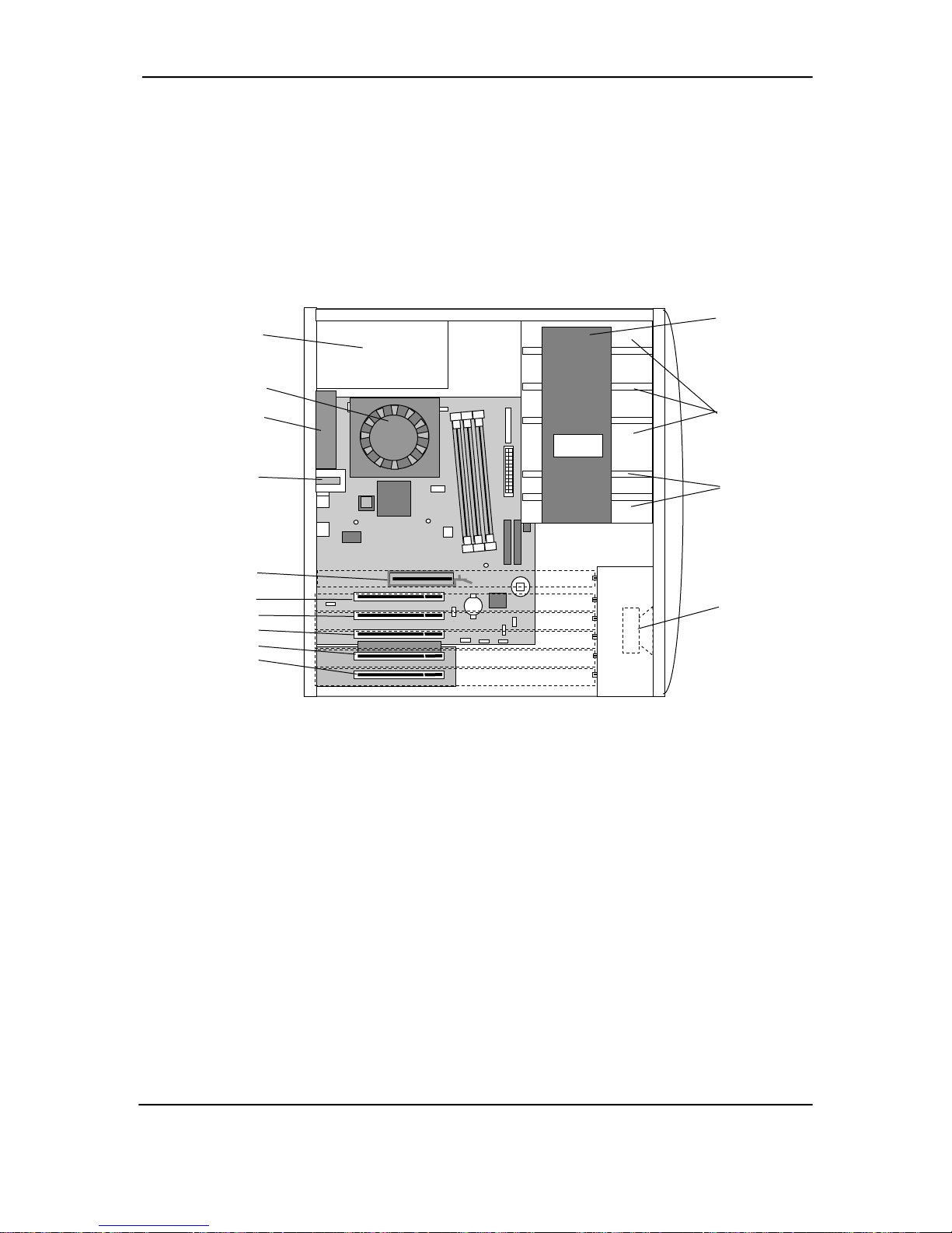
Technical Reference Guide
Figure 2-5 shows the layout for the Configurable Minitower in the minitower configuration.
Features include:
♦ Externally accessible drive bay assembly may be configured for minitower (vertical) or
desktop (horizontal) position.
♦ Easy access to expansion slots and all socketed system board components.
Power Supply
Processor/Heat Sink/Fan
Assembly
Chassis Fan
Hood Lock
Solenoid
(Optional)
Back
Drive Lock
Externally Accessible
Drive Bays
Internal
Drive Bays
Front
AGP Slot
PCI Slot 1
PCI Slot 2
PCI Slot 3
PCI Slot 4
PCI Slot 5
Speaker
Figure 2–6. Configurable Minitower Chassis Layout, Left Side View (Minitower configuration)
Compaq Evo and Workstation Personal Computers
Featuring the Intel Pentium 4 Processor
Second Edition - January 2003
2-9
Page 36

Chapter 2 System Overview
2.3.3 BOARD LAYOUTS
Figure 2-7 shows the system and riser boards for the small form factor unit.
27
24
32
31
30
29
28
26
25
1
System Board PCA# 011466-101 or 011351-001
Item Description
1 System board 17 Processor fan connector
2 Audio line in jack 18 Hard drive activity LED
3 Audio line out jack 19 Power button
4 USB connectors (2) 20 Power LED
5 Serial port A 21 USB ports (2)
6 Network interface connector 22 Audio headphones output jack
7 Battery 23 Audio microphone input jack
8 Parallel port 24 CD-ROM audio input connector
9 Serial port B 25 Diskette drive connector
10 Top: Mouse conn.; Bottom: keyboard conn. 26 Secondary IDE connector
11 Riser board slot 27 Primary IDE connector
12 Riser board 28 Power supply connector
13 PCI slot connectors (2) 29 Internal speaker connector
14 Hood (cover) sensor switch 30 CMOS clear button
15 Processor power connector 31 Hood (cover) lock solenoid connector
16 Processor socket (mPGA478) 32 DIMM sockets
NOTE:
Third DIMM socket present on PC133-based boards.
4 5
21
6
7
20
8
9
19
18
11
10
17
Riser Board SP# 252298-001
Item Description
3 2
22
23
13
12
14
15
16
Figure 2–7. Small Form Factor Board Layouts
Compaq Evo and Workstation Personal Computers
2-10
Featuring the Intel Pentium 4 Processor
Second Edition – January 2003
Page 37

Technical Reference Guide
Figure 2-7 shows the system and PCI slot expansion boards. The system board (with three PCI
slots) is common to both the desktop and the configurable minitower units. The PCI slot
expansion board is attached to the system board in the configurable minitower unit to provide a
total of 5 PCI slots.
1
3
2
5
6
4
7
9
8
10
11
12
13
14
34
33
32
15
16
17
18
19
31
30
29
23
22
28
27
26 25
24
21
20
PCI Slot Expansion Board [1]
SP# 252609-001
PCA# 011345-101 or 011348-101
System Board
Item Description
1 PCI slot expansion board [1] 18 Processor fan connector
2 PCI slots 19 DIMM sockets
3 System board 20 Power supply connector
4 Front panel headphone/microphone conn. 21 Diskette drive connector
5 AGP connector 22 SCSI hard drive LED connector
6 Top: NIC port; Bottom: USB ports (2) 23 Power button/Pwr & HD LED connector
7 Microphone Input jack 24 Primary IDE hard drive connector
8 Serial port (B) 25 Secondary IDE hard drive connector
9 Audio line input jack 26 CMOS clear button
10 Audio line output jack 27 Hood (cover) sense connector
11 Parallel port 28 Front panel USB port connector
12 Serial port (A) 29 Password clear jumper
13 Top: Mouse port; bottom: keyboard port 30 Chassis speaker connector
14 Processor power connector 31 CMOS battery
15 Processor socket 32 Auxiliary audio connector
16 Chassis fan connector 33 CD-ROM audio connector
17 Hood (cover) lock solenoid connector 34 PCI slot expansion connector
NOTE:
[1] Third DIMM socket present on PC133-type board (PCA# 011345) only.
[1] Used in configurable minitower units only.
Item Description
Figure 2–8. Desktop or Configurable Minitower Main Board Layouts
Compaq Evo and Workstation Personal Computers
Featuring the Intel Pentium 4 Processor
Second Edition - January 2003
2-11
Page 38

Chapter 2 System Overview
2.4 SYSTEM ARCHITECTURE
The Compaq Evo and Workstation systems covered in this guide feature an architecture based on
the Intel Pentium 4 processor and the Intel 845 chipset (Figure 2-9). These models use either
PC133 or DDR (PC266) SDRAM for system memory, provide AGP 4X graphics support, and
include PCI bus expansion capability.
The Intel 845 chipset includes the 82845 MCH designed to support the Pentium 4 processor with
an FSB speed of 400 MHz. The 82845 MCH also includes an SDRAM controller supporting up to
three PC133 DIMMs or two DDR DIMMs, depending on model configuration.
All systems feature AC’97-compatible audio subsystems and include a microphone input, a line
input and headphone and/or line output. The Small Form Factor system features Compaq Premier
Sound components while Desktop and Configurable Minitower systems provide a business audio
solution.
The 845 chipset also includes the 82801BA I/O Controller Hub (ICH2) that integrates two IDE
controllers with ATA100 support, two USB interfaces, and a PCI bus controller. Also integrated
into the 82801BA is an 82562 network interface controller. An SMC LPC47B367 Super I/O
Controller provides serial, parallel, keyboard, mouse, and diskette drive interface functions.
All models covered in this guide support ATA100-type hard drives. Select Compaq Workstation
W4000 models feature a SCSI PCI adapter controlling a Wide Ultra3 SCSI hard drive.
Below is a matrix defining the architectural differences based on form factor and series.
Series Type Evo/Workstation Evo Evo Workstation
SDRAM Memory Speed SDR SDR SDR SDR/DDR
Audio subsystem type Premier Sound Business Business Business
Front panel audio ports Standard Optional Optional Standard
Front panel USB ports Standard Optional Optional Standard
PCI slots 2 3 5 5
Hard Drive Type ATA100 ATA100 ATA100 ATA100 or SCSI
DDR = Double data rate
SDR = Single data rate
SFF Desktop Configurable Minitower
Compaq Evo and Workstation Personal Computers
2-12
Featuring the Intel Pentium 4 Processor
Second Edition – January 2003
Page 39

Technical Reference Guide
Pentium 4
Processor
Memory
Bus
System
Memory
Monitor
RGB
AGP 4X
Graphics
Controller
AGP
4X
I/F
400-MHz FSB
845 Chipset
82845
GMCH
SDRAM
Cntlr.
Hub Link
Bus
IDE
Hard Drive
Pri. IDE
Cntlr.
Sec. IDE
Cntlr.
CD
Audio
Audio
Subsystem
Beep
Audio
AC’97
Link Bus
SCSI
Hard Drive
Adaptec
29160N
SCSI
Adapter Card
82801BA
ICH2
PCI Slots
NIC
USB
Cntlr.
82802
FWH
33-MHz
32-Bit PCI Bus
LPC
Bus
Serial
I/F (2)
LPC47B367 I/O Controller
Keyboard/
Mouse I/F
Parallel
Diskette
I/F
I/F
Power
Supply
Select Workstation models only.
NOTES:
Figure 2–9. System Architecture, Block diagram
Compaq Evo and Workstation Personal Computers
Featuring the Intel Pentium 4 Processor
Second Edition - January 2003
2-13
Page 40

Chapter 2 System Overview
2.4.1 INTEL PENTIUM 4 PROCESSOR
The models covered in this guide feature the Intel Pentium 4 processor. This processor is
backward-compatible with software written for the Pentium III, Pentium II, Pentium MMX,
Pentium Pro, Pentium, and x86 microprocessors. The processor architecture includes a floatingpoint unit, 32-KB first and 512-KB secondary caches, and enhanced performance for multimedia
applications through the use of multimedia extension (MMX) instructions. Also included are
streaming SIMD extensions (SSE and SSE2) for enhancing 3D graphics and speech processing
performance. The Pentium 4 processor features Net-Burst Architecture that uses hyper-pipelined
technology and a rapid-execution engine that runs at twice the processor's core speed.
These systems employ an mPGA478B zero-insertion-force (ZIF) socket designed for mounting a
“Flip-Chip” (FC-PGA2) processor package (Figure 2-10). Small form factor units use a passive
heat sink held in place over the FC-PGA package with two retaining clips. Desktop and
configurable minitower units use an active assembly (which integrates the heat sink and fan) that
clips on to the processor socket over the FC-PGA package.
Heat Sink
Retaining Clips
Heat Sink for
Small Form Factor Units
(Shown in unlock position)
Figure 2–10. Processor Assembly And Mounting
Lock/Unlock
Handle
Heat Sink / Fan Assembly for
Desktop and
Configurable Minitower Units
FC-PGA2 Package
(w/ Integrated Heat
Spreader)
mPGA478B
Socket
These systems support processors fitted with passive heat sinks or processors fitted with heat
sink/fan assembly with a power cable that attaches to a fan-power header provided on the system
board. There are three types of passive heat sinks.
NOTE: The two types of heat sinks are not interchangeable. Also, these systems support
processors using the FC-PGA2 package only.
Compaq Evo and Workstation Personal Computers
2-14
Featuring the Intel Pentium 4 Processor
Second Edition – January 2003
Page 41

Technical Reference Guide
2.4.2 CHIPSET
The Intel 845 chipset consists of a Memory Controller Hub (MCH), an enhanced I/O controller
hub (ICH2), and a firmware hub (FWH). Table 2-2 lists the integrated functions provided by the
chipset.
Table 2-2. Chipset Comparison
Table 2-2.
845 Chipset Functions
Component Type Function
82845 MCH AGP 4X interface
82801BA ICH2 PCI bus I/F
82802 FWH Loaded with Compaq BIOS
[1] Dependent on system board type. System supports one or the other.
NOTE:
SDRAM controller supporting PC133 DIMMs or 266-MHz DDR DIMMs [1]
400-MHz FSB
LPC bus I/F
SMBus I/F
IDE I/F with UATA/100 support
AC ’97 controller
RTC/CMOS
IRQ controller
Power management logic
USB controllers #1 and #2 (supporting up to 4 ports)
Network interface controller
Random number generator
2.4.3 SUPPORT COMPONENTS
Input/output functions not provided by the chipset are handled by other support components.
Some of these components also provide “housekeeping” and various other functions as well.
Table 2-3 shows the functions provided by the support components.
Table 2-3. Support Component Functions
Support Component Functions
Component Name Function
LPC47B367 I/O Controller Keyboard and pointing device I/F
Diskette I/F
Serial I/F (COM1and COM2)
Parallel I/F (LPT1, LPT2, or LPT3)
AGP, PCI reset generation
Interrupt (IRQ) serializer
Power button logic
GPIO ports
AD1885 Audio Codec Audio mixer
Digital-to-analog converter
Analog-to-digital converter
Analog I/O
Table 2-3.
Compaq Evo and Workstation Personal Computers
Featuring the Intel Pentium 4 Processor
Second Edition - January 2003
2-15
Page 42

Chapter 2 System Overview
2.4.4 SYSTEM MEMORY
Two memory types are used in these systems:
♦ PC133-based with three DIMM sockets supporting up to 3 gigabytes of SDRAM memory
♦ 266-MHz DDR-based with two DIMM sockets supporting up to 2 gigabytes of DDR
memory.
NOTE: The maximum memory amounts stated above are with 1-GB memory modules
using 512 Mb technology DIMMs.
Industry-standard SDRAM DIMMs and DDR266 DIMMs are not interchangable in these
systems.
2.4.5 MASS STORAGE
All models include a 3.5 inch 1.44-MB diskette drive installed as drive A. Most models also
include a CD-ROM and either a 10-, 15-, or 20-GB hard drive. Standard hard drives feature Drive
Protection System (DPS) support. All systems provide two (one primary, one secondary) PCI
bus-mastering Enhanced IDE (EIDE) controllers integrated into the chipset. Each controller
provides UATA/100 support for two drives for a total of four IDE devices, although the form
factor will determine the actual number of drive spaces available.
2.4.6 SERIAL AND PARALLEL INTERFACES
All models include two serial ports and a parallel port accessible at the rear of the chassis. Each
serial port is RS-232-C/16550-compatible and supports standard baud rates up to 115,200 as well
as two high-speed baud rates of 230K and 460K, and utilize DB-9 connectors. The parallel
interface is Enhanced Parallel Port (EPP1.9) and Enhanced Capability Port (ECP) compatible, and
supports bi-directional data transfers through a DB-25 connector.
2.4.7 UNIVERSAL SERIAL BUS INTERFACE
All models feature a minimum of two Universal Serial Bus (USB) v1.1 ports that provide a
12Mb/s interface for peripherals. The Compaq Evo desktop and configurable minitower models
may be upgraded to include two additional USB ports on the front panel. All small form factor
and Workstation models include front panel USB ports in the standard configuration. The USB
provides hot plugging/unplugging (Plug ’n Play) functionality.
2.4.8 NETWORK INTERFACE CONTROLLER
All models feature a Network Interface Controller (NIC) integrated on the system board.
Equivalent to the Intel 82562 10/100 NIC, the controller provides automatic selection of 10BASET or 100BASE-TX operation with a local area network and includes power-down, wake-up, and
Alert-On-LAN features. An RJ-45 connector is provided on the rear panel.
Compaq Evo and Workstation Personal Computers
2-16
Featuring the Intel Pentium 4 Processor
Second Edition – January 2003
Page 43

Technical Reference Guide
2.4.9 GRAPHICS SUBSYSTEM
The 82845 MCH component includes an AGP 4X interface that supports an AGP graphics
controller installed in the AGP slot. The AGP slot includes both Type 1 and Type 2 retention
mechanisms. Dual-monitor support is possible by adding a PCI graphics card to the standard
configuration. Table 2-4 lists the key features of the standard graphics subsystems employed in
these systems:
Table 2-4. Standard Graphics Subsystem Comparison
Std. Config. In Evo Wkstn. W4000 Evo Wkstn. W4000
Recommended
for:
Bus Type AGP 4X AGP 4X AGP 4X PCI
Mem. Amount 16 MB 32 MB 16 / 32 MB 8 MB x 4
Mem. Type SGRAM SDRAM SDRAM SGRAM
DAC Speed 300 MHz 350 MHz 360 MHz (Pri)
Max. 2D Res.
Software
Compatibility
Aux. I/O VESA I/F VESA I/F VESA I/F VESA I/F
Outputs 1 RGB 1 RGB, 1 DVI [1] 2 RGB 4 RGB/4DVI [2]
NOTES:
[1] DVI connector on MXR card only.
[2] Supports up to four monitors.
Hi 2D,
1920x1200 1920x1200 2048x768 1920x1200
Quick Draw,
nVIDIA
Vanta
Entry 3D
DCI/DirectX,
Direct Draw,
Direct Show,
MPEG 1/2,
Indeo
Table 2-4.
Standard AGP Graphics Comparison
Quadro2 EX/MXR
nVIDIA
Hi 2D,
Entry 3D
Quick Draw,
DCI/DirectX,
Direct Draw,
Direct Show,
MPEG 1/2,
Indeo
Millennium
G450 Dual-Head
200 MHz (Sec)
Quick Draw,
DCI/DirectX,
Direct Draw,
Direct Show,
MPEG 1/2,
Matrox
Hi 2D,
Entry 3D
Indeo
Matrox
G200 MMS
Multi-monitor
Hi 2D
250 MHz
(analog mon.)
Quick Draw,
DCI/DirectX,
Direct Draw,
MPEG 1/2,
OpenGL,
Direct 3D
Compaq Evo and Workstation Personal Computers
Featuring the Intel Pentium 4 Processor
Second Edition - January 2003
2-17
Page 44

Chapter 2 System Overview
2.4.10 AUDIO SUBSYSTEM
These systems use the integrated AC97 audio controller of the 845 chipset and an AC’97compliant audio codec. These systems include microphone and line inputs and headphone and line
outputs. The Desktop and Configurable Minitower models include a 3-watt output amplifier
driving an internal speaker. The Small Form Factor models feature Compaq Premier Sound
consisting of a five-level equalizer designed to compensate for chassis acoustics and a lowdistortion 5-watt amplifier driving a speaker for optimum sound. Small form factor and all
Workstation models front panel-accessible audio jacks as standard while Evo desktop and
configurable minitower models may be upgraded to include front panel audio jacks.
2.5 SPECIFICATIONS
This section includes the environmental, electrical, and physical specifications for the Compaq
Evo and Worksstation Personal Computers. Where provided, metric statistics are given in
parenthesis. All specifications subject to change without notice.
Table 2-5. Environmental Specifications
Environmental Specifications (Factory Configuration)
Parameter Operating Nonoperating
Ambient Air Temperature 50o to 95o F (10o to 35o C, max. rate
Shock (w/o damage) 5 Gs [1] 20 Gs [1]
Vibration
Humidity
Maximum Altitude 10,000 ft (3048 m) [2] 30,000 ft (9,144 m) [2]
NOTE:
[1] Peak input acceleration during an 11 ms half-sine shock pulse.
[2] Maximum rate of change: 1500 ft/min.
Table 2-5.
o
-24
of change <
0.000215 G2/Hz, 10-300 Hz 0.0005 G2/Hz, 10-500 Hz
10-90% Rh @ 28o C max.
wet bulb temperature
10°C/Hr)
to 140o F (-30o to 60o C, max. rate
of change <
5-95% Rh @ 38.7o C max.
wet bulb temperature
20°C/Hr )
Table 2-6. Electrical Specifications
Electrical Specifications
Parameter U.S. International
Input Line Voltage:
Nominal:
Maximum:
Input Line Frequency Range:
Nominal:
Maximum:
Power Supply:
Maximum Continuous Power
Small Form Factor
Desktop
Configurable Minitower
Maximum Line Current Draw
Small Form Factor
Desktop
Configurable Minitower
Compaq Evo and Workstation Personal Computers
2-18
Featuring the Intel Pentium 4 Processor
Second Edition – January 2003
Table 2-6.
100 - 127 VAC
90 - 132 VAC
50 - 60 Hz
47 - 63 Hz
175 watts
235 watts
250 watts
2.7 A @ 100 VAC
3.6 A @ 100 VAC
3.6 A @ 100 VAC
200 - 240 VAC
180 - 264 VAC
50 - 60 Hz
47 - 63 Hz
175 watts
235 watts
250 watts
2.7 A @ 100 VAC
3.6 A @ 100 VAC
3.6 A @ 100 VAC
Page 45

Technical Reference Guide
Table 2-7. Physical Specifications
Table 2-7.
Physical Specifications
Parameter
Height 3.9 in (9.90 cm) 5.72 in (14.5 cm) 17.65 in (44.8 cm)
Width 13.1 in (33.3 cm) 15.25 in (38.7 cm) 6.60 in (16.8 cm)
Depth
Weight (nom.) [1]
Maximum Supported Weight [2] 100 lb (45.5 kg) 100 lb (45.5 kg) 100 lb (45.5 kg)
NOTES:
[1] System weight may vary depending on installed drives/peripherals.
[3] Minitower configuration. For desktop configuration, swap Height and Width dimensions.
[2] Assumes reasonable article(s) such as a display monitor and/or another system unit.
Small
Form Factor
14.4 in (36.6 cm) 17.90 in (45.5 cm) 16.80 in (42.7 cm)
20 lb (9.1 kg) 26 lb (12 kg) 26 lb (12 kg)
Desktop
Configurable
Minitower [3]
Table 2-8. Diskette Drive Specifications
Table 2-8.
Diskette Drive Specifications
(Compaq SP# 179161-001)
Parameter Measurement
Media Type 3.5 in 1.44 MB/720 KB diskette
Height 1/3 bay (1 in)
Bytes per Sector 512
Sectors per Track:
High Density
Low Density
Tracks per Side:
High Density
Low Density
Read/Write Heads 2
Average Access Time:
Track-to-Track (high/low)
Average (high/low)
Settling Time
Latency Average
18
9
80
80
3 ms/6 ms
94 ms/173ms
15 ms
100 ms
Compaq Evo and Workstation Personal Computers
Featuring the Intel Pentium 4 Processor
Second Edition - January 2003
2-19
Page 46

Chapter 2 System Overview
Table 2-9. Optical Drive Specifications
Parameter 48x CD-ROM 16/10/40x CD-RW Drive
Interface Type IDE IDE
Media Type (reading)
Media Type (writing) N/a CD-R, CD-RW
Transfer Rate (Reads) 4.8 Kb/s (max sustained) CD-ROM, 4.8 Kb/s;
Transfer Rate (Writes): N/a CD-R, 2.4 Kbps (sustained);
Capacity:
Mode 1, 12 cm
Mode 2, 12 cm
8 cm
Center Hole Diameter 15 mm 15 mm
Disc Diameter 8/12 cm 8/12 cm
Disc Thickness 1.2 mm 1.2 mm
Track Pitch 1.6 um 1.6 um
Laser
Beam Divergence
Output Power
Type
Wave Length
Average Access Time:
Random
Full Stroke
Audio Output Level 0.7 Vrms 0.7 Vrms
Cache Buffer 128 KB 128 KB
Table 2-9.
Optical Drive Specifications
Mode 1,2, Mixed Mode, CD-DA,
Photo CD, Cdi, CD-XA
550 MB
640 MB
180 MB
53.5
+/- 1.5 °
53.6
0.14 mW
GaAs
790 +/- 25 nm
<100 ms
<150 ms
Mode 1,2, Mixed Mode, CD-DA,
Photo CD, Cdi, CD-XA
CD-ROM/CD-R, 1.5-6 Kb/s
CD-RW, 1.5 Kbps (sustained);
650 MB @ 12 cm
53.5 + 1.5°
53.6 0.14 mW
GaAs
790 +/- 25 nm
<120 ms
<200 ms
Table 2-10. Hard Drive Specifications
Hard Drive Specifications
Parameter 20.0 GB 32.0 GB 40.0 GB 60.0 GB
Drive Size 3.5” 3.5" 3.5” 3.5”
Interface UATA/100 Ultra3 SCSI UATA/100 UATA/100
Transfer Rate 100 MBps 160 MBps 100 MBps 100 MBps
Drive Protection System Support? Yes Yes Yes Yes
Typical Seek Time (w/settling) [1]
Single Track
Average
Full Stroke
Disk Format (logical blocks) 39,102,336 71,132,000 78,165,360 78,165,360
Rotation Speed 7200 RPM 10,000 RPM 7200 RPM 7200 RPM
Drive Fault Prediction SMART III N/a SMART III SMART III
NOTE:
Actual times may vary depending on specific drive installed.
All ATA drives are Quiet Drives.
Compaq Evo and Workstation Personal Computers
2-20
Featuring the Intel Pentium 4 Processor
Second Edition – January 2003
Table 2-10.
1.2 ms
8.0 ms
18 ms
0.6 ms
4.7 ms
12 ms
1.2 ms
8.0 ms
18 ms
1.0 ms
9.0 ms
20 ms
Page 47

Technical Reference Guide
Chapter 3
PROCESSOR/
MEMORY SUBSYSTEM
3. Chapter 3 PROCESSOR/MEMORY SUBSYSTEM
3.1 INTRODUCTION
This chapter describes the processor/memory subsystem of Compaq Deskpro Personal Computers
featuring the Pentium 4 processor. These systems feature the Pentium 4 processor and the 845
chipset (Figure 3-1). The 82845 MCH component of the 845 chipset supports SDRAM memory
of either the standard PC133 or the DDR type, depending on model.
Pentium 4
Processor
400-MHz
64-Bit FSB
AGP
I/F
Present in PC133 systems only.
Covered in Chapter 4
FSB I/F
82845
MCH
Hub I/F
Cntl
Memory
Cntlr.
XMM1
Mem. Bus
DIMM
In
Socket
System Memory
XMM2
DIMM
Socket
XMM3
DIMM
Socket
Figure 3–1. Processor/Memory Subsystem Architecture
This chapter includes the following topics:
♦ Pentium 4 processor [3.2] page 3-2
♦ Memory subsystem [3.3] page 3-5
♦ Subsystem configuration {3.4] page 3-8
Compaq Evo and Workstation Personal Computer
Featuring the Intel Pentium 4 Processor
Second Edition - January 2003
3-1
Page 48

Chapter 3 Processor/Memory Subsystem
3.2 PENTIUM 4 PROCESSOR
These systems each feature an Intel Pentium 4 processor in a FC-PGA478 package mounted with
a passive heat sink in a mPGA478B zero-insertion force socket. The mounting socket allows the
processor to be easily changed for servicing and/or upgrading.
3.2.1 PROCESSOR OVERVIEW
The Intel Pentium 4 processor represents the latest generation of Intel’s IA32-class of processors.
Featuring Intel’s NetBurst architecture, the Pentium 4 processor is designed for intensive
multimedia and internet applications of today and the future while maintaining compatibility with
software written for earlier (Pentium III, Pentium II, Pentium, Celeron, and x86) microprocessors.
Key features of the Pentium 4 processor include:
♦ Hyper-Pipelined Technology – The main processing loop has twice the depth (20 stages) of
the Pentium III allowing for increased processing frequencies.
♦ Execution Trace Cache – A new feature supporting the branch prediction mechanism, the
trace cache stores translated sequences of branching micro-operations (µops) and is checked
when suspected re-occurring branches are detected in the main processing loop. This feature
allows instruction decoding to be removed from the main processing loop.
♦ Rapid Execution Engine – Arithmetic Logic Units (ALUs) run at twice (2x) processing
frequency for higher throughput and reduced latency.
♦ 256-KB Advanced transfer L2 cache – Using 32-byte-wide interface at processing speed, the
L2 cache can provide 48 GB/s performance (3x over the Pentium III)
♦ Advanced dynamic execution – Using a larger (4K) branch target buffer and improved
prediction algorithm, branch mis
Pentium III.
♦ Enhanced Floating Point Processor - With 128-bit integer processing and deeper pipelining
the Pentium 4’s FPU provides a 2x performance boost over the Pentium III.
♦ Additional Streaming SIMD extensions (SSE2) – In addition to the SSE support provided by
previous Pentium processors, the Pentium 4 processor includes an additional 144 MMX
instructions, further enhancing:
• Streaming video/audio processing
• Photo/video editing
• Speech recognition
• 3D processing
• Encryption processing
♦ Quad-pumped Front Side Bus (FSB) – The FSB uses a 100-MHz clock for qualifying the
buses’ control signals. However, address information is transferred using a 200-MHz strobe
while data is transferred with a 400-MHz strobe, providing a maximum data transfer rate of
3.2 GB/s. This is a boost of over three times that of a Pentium III with a 133-MHz FSB.
-predictions are reduced by an average of 33 % over the
Compaq Evo and Workstation Personal Computers
3-2
Featuring the Intel Pentium 4 Processor
Second Edition - January 2003
Page 49

Technical Reference Guide
Figure 3-1 illustrates the internal architecture of the Pentium 4 processor.
Pentium 4 Processor
L1
Data
Cache
256-KB
8-Way
Transfer
Cache
L2
Adv.
Branch
Prediction
Rapid Exe. Eng.
ALUs
Trace Cache
CPU
Execution
Out-of-
Order Core
128-bit
Integer
FPU
FSB
I/F
ALU Speed: Core speed x2
Core Speed: 1.4, 1.5, 2.0, 2.2 GHz
FSB Speed: 400 MHz (effective data transfer rate)
Figure 3–2. Pentium 4 Processor Internal Architecture
The Pentium 4 increases processing speed with higher clock speeds made possible with hyperpipelined technology that can handle significantly more instructions at a time. Since branch mispredicts would result in serious performance hits with such a long pipeline, the Pentium 4 features
a branch prediction mechanism improved with the addition of an execution trace cache and a
refined prediction algorithm. The execution trace cache can store 12k micro-ops (decoded
instructions dealing with branching sequences) that are checked when re-occurring branches are
processed. Code that is not executed (bypassed) is no longer stored in the L1 cache as was the
case in the Pentium III.
The out-of-order core features Advanced Dynamic Execution, which provides a large window
(126 instructions) for execution units to work with. A more accurate branch prediction algorithm,
along with a larger (4-KB) branch target buffer that stores more details on branch history results
in a 33% reduction in branch mis-predictions over the Pentium III.
The L1 data cache features a low-latency design for minimum response to cache hits. The 256-KB
advanced transfer L2 cache features a 256-bit (32-byte) interface operating at processing speed.
The L2 cache of the 1.5 GHz Pentium 4 can therefore provide a transfer rate of 48 GB/s.
The combined improvements of the Pentium 4’s CPU core the rapid execution engine’s ALUs to
operate at twice the processing frequency to handle the steady stream of instructions.
The front side bus (FSB) of the Pentium 4 uses a 100-MHz clock but provides bi- and quadpumped transfers through the use of 200- and 400-MHz strobes. The Pentium 4 can transfer a
complete 64-byte cache line in two 100-MHz bus cycles for a throughput rate of 3.2 GB/s.
Address information is transferred at a 200-MHz rate.
Compaq Evo and Workstation Personal Computer
Featuring the Intel Pentium 4 Processor
Second Edition - January 2003
3-3
Page 50

Chapter 3 Processor/Memory Subsystem
The Pentium 4 processor is software-compatible with Celeron, Pentium II, Pentium MMX,
Pentium, and x86 processors, but will require the latest versions of operating system software to
take advantage of the Streaming SIMD extensions (SSE2).
3.2.2 PROCESSOR UPGRADING
All units use mPGA478B ZIF mounting socket and ship with the Pentium 4 processor in a FlipChip (FC-PGA478) package installed with a passive heat sink. The FC-PGA478 package consists
of the processor die mounted “upside down” on a PC board. This arrangement allows the heat
sink to come in direct contact with the processor die. The heat sink and attachment clip are
specially designed provide maximum heat transfer from the processor component.
CAUTION: Attachment of the heat sink to the processor is critical on these systems.
!
Improper attachment of the heat sink will likely result in a thermal condition.
Although the system is designed to detect thermal conditions and automatically shut
down, such a condition could still result in damage to the processor component. Refer to
the applicable Maintenance and Service Guide for processor installation instructions.
Compaq Evo and Workstation Personal Computers
3-4
Featuring the Intel Pentium 4 Processor
Second Edition - January 2003
Page 51

Technical Reference Guide
3.3 MEMORY SUBSYSTEM
These systems support one of two types of memory: single data rate (SDR) SDRAM or double
data rate (DDR) SDRAM. The system board determines the type of memory supported:
♦ SDR SDRAM-based system board: Three 168-pin DIMM sockets that accept PC100 or
PC133 (PC133 supplied) DIMMs.
♦ DDR SDRAM-based system board: Two 184-pin DIMM sockets that accept PC1600 or
PC2100 (PC2100 supplied) DIMMs.
NOTE: The two memory types are not interchangeable within a system. The system
board determines memory type.
NOTE: The SDR SDRAM "PCxxx" reference designates bus speed (i.e, a PC133
DIMM is designed for 133 MHz operation). The DDR SDRAM "PCxxxx" reference
designates bus bandwidth (i.e., a PC2100 DIMM can, operating at a 266-MHz effective
speed, provide a throughput of 2100 MBps (8 bytes × 266 MHz)).
These systems accept DIMMs with the following parameters:
♦ Unbuffered, compatible with SPD rev. 1.0
♦ 32-, 64-, 128-, 256-, and 512-Mb memory technology
♦ Single or double-sided
NOTE: Systems that support DDR SDRAM accept either ECC or non-ECC DIMMs,
but not both.
The SPD format supported by these systems complies with the JEDEC specification for 128-byte
EEPROMs. This system also provides support for 256-byte EEPROMs to include additional
Compaq-added features such as part number and serial number. The SPD format as supported in
this system (SPD rev. 1) is shown in Table 3-3.
The key SPD bytes that BIOS checks for compatibility are 2, 9, 10, 18, 23, 24, and 126. If BIOS
detects EDO or ECC DIMMs a “memory incompatible” message will be displayed and the
system will halt. This system is designed for using non-ECC DIMMs only. Refer to chapter 8
for a description of the BIOS procedure of interrogating DIMMs.
An installed mix of DIMM types (PC100 and PC133, CL 2 and CL 3) is acceptable but operation
will be constrained to the level of the DIMM with the lowest performance specification.
If an incompatible DIMM is detected the NUM LOCK will blink for a short period of time during
POST and an error message may or may not be displayed before the system hangs.
Compaq Evo and Workstation Personal Computer
Featuring the Intel Pentium 4 Processor
Second Edition - January 2003
3-5
Page 52

Chapter 3 Processor/Memory Subsystem
The SPD address map is shown below.
Table 3–1. SPD Address Map (SDRAM DIMM)
SPD Address Map (SDRAM DIMM)
Byte Description Notes Byte Description Notes
0 No. of Bytes Written Into EEPROM [1] 25 Min. CLK Cycle Time at
1 Total Bytes (#) In EEPROM [2] 26 Max. Acc. Time From
2 Memory Type 27 Min. Row Prechge. Time [7]
3 No. of Row Addresses On DIMM [3] 28 Min. Row Active to Delay [7]
4 No. of Column Addresses On DIMM 29 Min. RAS to CAS Delay [7]
5 No. of Module Banks On DIMM 30, 31 Reserved
6, 7 Data Width of Module 32..61 Superset Data [7]
8 Voltage Interface Standard of DIMM 62 SPD Revision [7]
9 Cycletime @ Max CAS Latency (CL) [4] 63 Checksum Bytes 0-62
10 Access From Clock [4] 64-71 JEP-106E ID Code [8]
11 Config. Type (Parity, Nonparity, etc.) 72 DIMM OEM Location [8]
12 Refresh Rate/Type [4] [5] 73-90 OEM’s Part Number [8]
13 Width, Primary DRAM 91, 92 OEM’s Rev. Code [8]
14 Error Checking Data Width 93, 94 Manufacture Date [8]
15 Min. Clock Delay [6] 95-98 OEM’s Assembly S/N [8]
16 Burst Lengths Supported 99-125 OEM Specific Data [8]
17 No. of Banks For Each Mem. Device [4] 126 Intel frequency check
18 CAS Latencies Supported [4] 127 Reserved
19 CS# Latency [4] 128-131 Compaq header “CPQ1” [9]
20 Write Latency [4] 132 Header checksum [9]
21 DIMM Attributes 133-145 Unit serial number [9] [10]
22 Memory Device Attributes 146 DIMM ID [9] [11]
23 Min. CLK Cycle Time at CL X-1 [7] 147 Checksum [9]
24 Max. Acc. Time From CLK @ CL X-1 [7] Reserved [9]
NOTES:
[1] Programmed as 128 bytes by the DIMM OEM
[2] Must be programmed to 256 bytes.
[3] High order bit defines redundant addressing: if set (1), highest order RAS# address must be
re-sent as highest order CAS# address.
[4] Refer to memory manufacturer’s datasheet
[5] MSb is Self Refresh flag. If set (1), assembly supports self refresh.
[6] Back-to-back random column addresses.
[7] Field format proposed to JEDEC but not defined as standard at publication time.
[8] Field specified as optional by JEDEC but required by this system.
[9] Compaq usage. This system requires that the DIMM EEPROM have this
space available for reads/writes.
[10] Serial # in ASCII format (MSB is 133). Intended as backup identifier in case vender data is
invalid.
Can also be used to indicate s/n mismatch and flag system adminstrator of possible system
Tampering.
[11] Contains the socket # of the module (first module is “1”). Intended as backup identifier (refer to
note [10]).
Table 3-3.
[7]
CL X-2
[7]
CLK @ CL X-2
Compaq Evo and Workstation Personal Computers
3-6
Featuring the Intel Pentium 4 Processor
Second Edition - January 2003
Page 53

Technical Reference Guide
Figure 3-4 shows the system memory map.
Host,
PCI, AGP Area
FFFF FFFFh
FFE0 0000h
FFDF FFFFh
FEC1 0000h
FEC0 FFFFh
FEC0 0000h
FEBF FFFFh
High BIOS Area
(2 MB)
PCI Memory
(18 MB)
APIC Config. Space
(64 KB)
PCI Memory
Expansion
(3060 MB)
4 GB
Host, PCI,
ISA Area
DOS Compatibility
Area
2000 0000h
1FFF FFFFh
0100 0000h
00FF FFFFh
0010 0000h
000F FFFFh
000F 0000h
000E FFFFh
000E 0000h
000D FFFFh
000C 0000h
000B FFFFh
000A 0000h
0009 FFFFh
0008 0000h
0007 FFFFh
Host/PCI Memory
Expansion
(496 MB)
Extended Memory
(15 MB)
System BIOS Area
(64 KB)
Extended BIOS
Area
Option ROM
(128 KB)
Graphics/SMRAM
RAM (128 KB)
Fixed Mem. Area
(128 KB)
Base Memory
(512 KB)
512 MB
16 MB
1 MB
640 KB
512 KB
0000 0000h
NOTE: All locations in memory are cacheable. Base memory is always mapped to DRAM. The next 128 KB
fixed memory area can, through the north bridge, be mapped to DRAM or to PCI space. Graphics RAM area is
mapped to PCI or AGP locations.
Figure 3–3. System Memory Map
Compaq Evo and Workstation Personal Computer
Featuring the Intel Pentium 4 Processor
Second Edition - January 2003
3-7
Page 54

Chapter 3 Processor/Memory Subsystem
3.4 SUBSYSTEM CONFIGURATION
The 82815 GMCH component provides the configuration function for the processor/memory
subsystem. Table 3-4 lists the configuration registers used for setting and checking such
parameters as memory control and PCI bus operation. These registers reside in the PCI
Configuration Space and accessed using the methods described in Chapter 4, section 4.2.
Table 3–2. Host/PCI Bridge Configuration Registers (GMCH, Function 0)
Table 3-4.
Host/PCI Bridge Configuration Registers (GMCH, Device 0)
PCI Config.
Addr.
00, 01h Vender ID 8086h 6A, 6Bh DRAM Control Reg. 00h
02, 03h Device ID 1130h 6C..6Fh Memory Buffer Strength 55h
04, 05h Command 0006h 70h Multi-Transaction Timer 00h
06, 07h Status [1] 71h CPU Latency Timer 10h
08h Revision ID -- 72h SMRAM Control 02h
0A..0Bh Class Code -- 90h Error Command 00h
0Dh Latency Timer 00h 91h Error Status Register 0 00h
0Eh Header Type 00h 92h Error Status Register 1 00h
10..13h Aperture Base Config. [2] 93h Reset Control 00h
50, 51h PAC Config. Reg. 00h A0..A3h AGP Capability Identifier N/A
53h Data Buffer Control 83h A4..A7h AGP Status N/A
55..56h DRAM Row Type 00h A8..ABh AGP Command 00h
57h DRAM Control 01h B0..B3h AGP Control 00h
58h DRAM Timing 00h B4h Aperture Size 0000h
59..5Fh PAM 0..6 Registers 00h B8..BBh Aperture Translation Table 0000h
60..67h DRAM Row Boundary 01h BCh Aperture I/F Timer 00h
68h Fixed DRAM Hole 00h BDh Low Priority Timer 00h
NOTES:
Register
Refer to Intel Inc. documentation for detailed description of registers.
Assume unmarked locations/gaps as reserved.
[1] = 0090h for AGP (external graphics) implementation; = 0080h for GFX (internal i740)
implementation.
[2] = 8 for AGP; = 0 for GFX.
Reset
Value
PCI Config.
Addr.
Register
Reset
Value
Compaq Evo and Workstation Personal Computers
3-8
Featuring the Intel Pentium 4 Processor
Second Edition - January 2003
Page 55

Technical Reference Guide
Chapter 4
SYSTEM SUPPORT
4. Chapter 4 SYSTEM SUPPORT
4.1 INTRODUCTION
This chapter covers subjects dealing with basic system architecture and covers the following
topics:
♦ PCI bus overview (4.2) page 4-2
♦ AGP bus overview (4.3) page 4-10
♦ System resources (4.4) page 4-15
♦ System clock distribution (4.5) page 4-22
♦ Real-time clock and configuration memory (4.6) page 4-23
♦ System management (4.7) page 4-33
♦ Register map and miscellaneous functions (4.8) page 4-38
This chapter covers functions provided by off-the-shelf chipsets and therefore describes only basic
aspects of these functions as well as information unique to the systems covered in this guide. For
detailed information on specific components, refer to the applicable manufacturer’s
documentation.
Compaq Evo and Workstation Personal Computers
Featuring the Intel Pentium 4 Processor
Second Edition - January 2003
4-1
Page 56

Chapter 4 System Support
4.2 PCI BUS OVERVIEW
NOTE: This section describes the PCI bus in general and highlights bus implementation
in this particular system. For detailed information regarding PCI bus operation, refer to
the PCI Local Bus Specification Revision 2.2.
These systems implement a 32-bit Peripheral Component Interconnect (PCI) bus (spec. 2.2)
operating at 33 MHz. The PCI bus handles address/data transfers through the identification of
devices and functions on the bus. A device is typically defined as a component or slot that resides
on the PCI bus (although some components such as the MCH and ICH2 are organized as multip
devices). A function is defined a
ontain one or more functions.
c
In the standard configuration these systems use a hierarchy of three PCI buses (Figure 4-1). The
PCI bus #0 is internal to the 815E chipset components and is not physically accessible. T
bus that services the AGP slot (or resident AGP controller on the Small Form Factor) is
designated as
CI bus #2.
P
NOTES:
PCI bus #1. All PCI slots and the NIC function internal to the 82801BA reside on
M omponent
82845 CH C
Mem. Cntlr.
Function
Hub Link
Hub Link I/F
PCI Br
Func
[1] Desktop and Configurable minitower models only
[2] Configurable minitower models only
I/F
Hub
idge
tion
PCI
Bus #2
PCI
Bus #2
Link Bus
s the end source or target of the bus transaction. A device may
PCI Bus #1
(AGP Bus)
AGP Connector
PCI
Bus #0
AGP
Bridge
Function
NIC
I/F
Function
82801BA ICH2 Component
PCI Bus #0
EIDE USB SMBus LPC AC97
Controller
Function
I/F
Function
Controller
Function
Function
PCI Connector 1
PCI Connector 2
PCI Connector 3 [1]
PCI Connector 4 [2]
PCI Connector 5 [2]
.
he AGP
Bridge
le
Audio
Function
Compaq Evo and Workstation Personal Computers
4-2
Featuring the Intel Pentium 4 Processor
Second Edition – January 2003
Page 57

Technical Reference Guide
Figure 4-1. PCI Bus Devices and Functions
Compaq Evo and Workstation Personal Computers
Featuring the Intel Pentium 4 Processor
Second Edition - January 2003
4-3
Page 58

Chapter 4 System Support
4.2.1
PCI BUS TRANSACTIONS
The PCI bus consists of a 32-bit path (AD31-00 lines) that uses a multiplexed scheme for
handling both address and data transfers. A bus transaction consists of an address cycle and one
or more data cycles, with each cycle requiring a clock (PCICLK) cycle. High performance is
realized during burst modes in which a transaction with contiguous memory locations requires
at only one address cycle be conducted and subsequent data cycles are completed using auto-
th
cremented addressi
in n Four types of d ss n
onf p bus).
c iguration, and s ddress dec PC
g. ad re cycl
ecial. A odin but p to vic e I
4.2.1.1 I/O and Memory Cycles
For I/O ecode (AD31..0) for byte-level addressing
and memory cycles, a standard 32-bit address d
is handled by the appropriate PCI device. For memory addressing, PCI devices decode the
AD31..2 lines for dword-level addr
essing and check the AD1,0 lines for burst (linearincrementing) mode. In burst mode, subsequent data phases are conducted a dword at a time with
addressing assumed to increment accordingly (four bytes at a time).
4.2.1.2 Configuration Cycles
evices on the PC ply wi PCI protoc at allows figurati of that dev
D I bus must com th ol th con on ice by
oftware. In th io echani h Bus
s is system, configurat n m sm #1 (as described in t e PCI Local
specification Rev. 2.1) is employed. This method uses two 32-bit registers for initiating a
configuration cycle for accessing the configura n space o device e configuration
ddress reg S 8h alue that specifies the PCI bus, PCI
a ister (CONFIG_ADDRE S) at 0CF holds a v
device, and specific register to be a essed. Th onfigura registe CONFIG ATA) at
CFCh contain
0 s the configuration data.
P dress Register
CI Configuration Ad
I/O Port 0CF8h, R/W, (32-bit access only)
Bit
30..24 Reserved - rea
23..16 Bus Number. S I bus
15..11 PCI Device Nu ects PC
10..8
7..2
1,0
Function it Fun
31 Configuration En
0 = Disabled
1 = Enable
device for acc
Function Number. Selects function of
selected PCI devic
Register Index. Specifies config. reg.
Configuration Cycle Type ID.
00 = Type 0
01 = Type 1
able
d/write 0s
elects PC
mber. Sel I
ess
Compaq Evo and Workstation Personal Computers
4-4
Featuring the Intel Pentium 4 Processor
cc e c tion data r ( _D
e.
Second Edition – January 2003
es ca take pl
g is distri
ed (left u
ace on the P
tio f a PCI . Th
PCI Configuration Data Register
I/O Port 0CFCh, R/W, (8-, 16-, 32-bit access)
B ction
31..0 Configuration Data.
each de
CI bus; I/
e on th
O, memory,
Page 59

Technical Reference Guide
Two types of configuration cycles are used. A Type 0 (zero) cycle is targeted to a device on the
PCI bus on which the cycle is running. A Type 1 cycle is targeted to a device on a downstream
R
egister
Index
I bridge
PCI bus as identified by bus number bits <23..16>. With three or more PCI buses, a PC
device being serviced by that bridge or it
may convert a Type 1 to a Type 0 if it’s de
ay forward the Type 1 cycle unmodified dest
ow bri c
d nstream dge. Figure 4-2 shows the onfigurat format a how th din of
CF8h res iguration cycle on th
0 ults in a Type 0 conf evice Number (bits <15..11>
etermines which one of the AD31..11 line
d s is to
a ct n I
acts as “chip sele ” functio for the PC device t figured. The f n numb (CF8h,
its <10..8>) i elect a particular f on wi
b s used to s uncti I component.
Register 0C
R
esults in:
AD31..0
(w/Type 00
C
onfig. Cycle)
F8h
3
Reserved
IDSEL (only one signal li
stined fo
if it ism
22
r a
ined for a device being serviced by a
on cycle nd e loa g
i
e PCI bus. The D
be asserted high for the IDSEL signal, which
be con unctio er
o
thin a PC
1
Bu
Num
1
s
ber
ne asser
118 7 2 1 0 [1]
Devic
e Function Register
Numb
er Number Index
tion
ted)
Func
Numb
er
NOTES:
[1] Bits <1,0> : 00 = Typ
Type 01 c
ycle only. Reserved on Ty cy
e 1 e 1
0 Cycle, 0 = Typ
pe 00
cycle
cle.
igure 4-2. Configuration Cycle
F
Table 4-1 shows the standard configur ers and IDSEL connections for
omponents and slots residing on a PCI bus.
c
Table 4-1. PCI Device Configu
ation of device numb
ration Access
PCI Component Confi
PCI Component
82845 MCH:
Memory Controller
AGP Bridge
AGP slot 0 0 (00h) 1 -82801BA ICH2:
PCI Bridge
LPC Bridge
EIDE Controller
USB I/F #1
SMBus Co
USB I/F #2
AC97 Audio
AC97 Modem Contr
Network Inter
PCI Connector 1 (slot 1) [2] 0 4 (04h) 2 AD20
PCI Connector 2 (slot 2) [2] 2 AD25 0 9 (09h)
PCI Connector 3 (slot 3) [2, 3] ) 2 AD26 0 10 (0Ah
PCI Connector 4 (slot 4) [2, 4] 2 AD27 0 11 (0Bh)
PCI Connector 5 (slot 5) [2, 4] ) 2 AD29 0 13 (0Dh
OTES:
ed.
[3] Desktop and Configurable Minitow
[4] Configu
N
ntroller
Controller
oller
face Controller
[1] Not implement
[2] PCI bus number giv
rable minitower models only.
Notes
[1]
en is for standard configuration.
Table 4-1.
guration Access
Function # Device #
0
0
0
0
1
2
3
4
5
6
0
er models only.
0 (00h)
1 (01h)
30 (1Eh)
31 (1Fh)
31 (1Fh)
31 (1Fh)
31 (1Fh)
31 (1Fh)
31 (1Fh)
31 (1Fh)
8 (08h)
PCI
Bus #
0
0
0
0
0
0
0
0
0
0
2
IDSEL
Wired to:
--
--
Compaq Evo and Workstation Personal Computers
Featuring the Intel Pentium 4 Processor
Second Edition - January 2003
4-5
Page 60
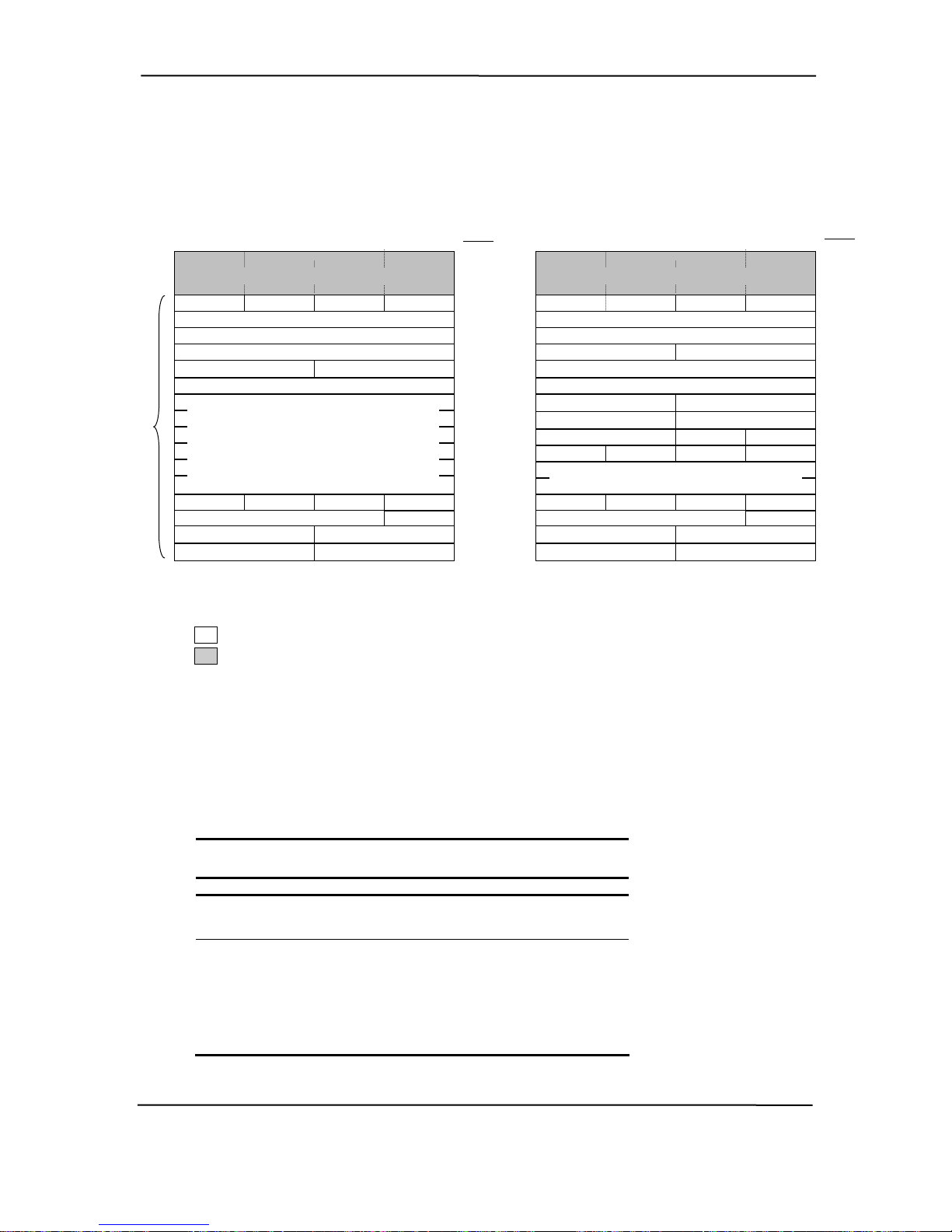
Chapter 4 System Support
d
yp
yp
T
he register index (CF8h, bits <7..2>) identifies the 32-bit location within the configuration space
of the PCI device to be accessed. All PCI devices can contain up to 256 bytes of configuration
data (Figure 4-3), of which the first 64 bytes comprise the configuration space header.
Configuration
Space
Header
31
24 23 16 15 8 7 0
Device-Specific Area
M
Expansion ROM Base Address
Reserved
Reserved
Subsystem Vendor ID Subsystem ID
Card Bus CIS Pointer
Base Address Regist s er
IST Hdr. T
Status
Devi
e
Command
Vendor ID ce ID
PCI Configuration Space Type 0
Data required by PCI protocol
Not required
Register
Index
FCh
Int. Line Int. Pin Min. GNT in. Lat.
Line Size Lat. Timer B
40h
3Ch
38h
34h
30h
2Ch
28h
10h
0Ch
08h
04h
00h
31 24 23 16 15 8 7 0
Device-Specific Area
Int. Line Int. Pin Bridge Control
Expansion ROM Base Address
Reserved
I/O Base Upper 16 Bits
Prefetchable Limit Upper 32 Bits
Prefetchable Base Upper 32 Bits
Prefetch. Mem. Limit Prefetch. Mem. Base
Memory Base Memory Limit
ondary Status
n
Lat.Tmr
BIST Hd
Status
Sub. Bus # 2
Bas
e Address Registers
e
I/O Base I/O Limit Sec
Pri. Bus # Sec. Bus #
Line Size Lat. Timer r. T
Command
Vendor ID Device ID
Register
Index
FCh
40h
3Ch
38h
34h
30h
2Ch
28h
24h
20h
1Ch
18h
10h
0Ch
08h
04h
00h
PCI Configuration Space Type 1
Figure 4-3. PCI Configuration Space Mapping
ach PCI device is identified with a vendor ID (assigned to the vendor by the PCI Special Interest
E
Group) and a device ID (assigned by the vendor). The device and vendor IDs for the devices on
the system board are listed in Table 4-2.
Table 4-2. System Board PCI Device Identification
Table 4-2.
System Board PCI Device Identification
PCI Device Vendor ID Device ID
82845 MCH:
Memory Controller
AGP Bridge
82801 ICH2:
PCI Bridge
LPC Bridge
EIDE Controller
USB I/F #2
SMBus Controller
AC97 Audio Controller
Network Interface Controller
Compaq Evo and Workstation Personal Computers
4-6
Featuring the Intel Pentium 4 Processor
Second Edition – January 2003
8086h
8086h
8086h
8086h
8086h
8086h
8086h
8086h
8086h
1A30h
1A31h
244Eh
2440h
244Bh
2444h
(Hidden)
2445h
2449h
Page 61

Technical Reference Guide
4.2.2 PCI BUS MASTER ARBIT
The PCI bus supports a bus master/target arbitration scheme. A bus master is a device that has
been granted control of the bus for the purpose of initiating a transaction. A target is a device th
is the recipient of a transaction. The Request (REQ), Grant (G
by PCI bus masters for gaining access to the PCI bus. When a PCI device needs access to the PCI
bus (and does not already own it), the PCI device asserts it’s REQn signal to the PCI bus arbiter (a
function of the system control
signal to the requesting device, which then asserts FRAME and conducts the address phase of the
transaction with a target. If the PCI device already owns the bus, a request is not needed and the
device can simply assert FRAME and conduct the transaction. Table 4-3 shows the grant and
request signals assignments for the devices on the PCI bus.
e 4-3. PCI Bus Mastering Devices
Tabl
PCI Bus Mastering Devices
REQ/GNT Line Device
REQ0/GNT0 PCI Connector Slot 1
REQ1/GNT1 PCI Connector Slot 2
REQ2/GNT2 PCI Connector Slot 3 [1]
REQ3/GNT3 PCI Connector Slot 4 [2]
REQ4/GNT4 PCI Connector Slot 5 [2]
GREQ/GGNT AGP Slot
NOTE:
[1] Desktop and Config
[2] Configurable minito
CI bus arbitration is based on a round-robin scheme that complies with the fairness algorithP
ecified by the PCI specification. The bus parking policy allows for the current PCI bus owner
sp
(excepting the PCI/ISA br
a t most CPU-to-DRAM and AGP-to-DRAM accesses can occur
by nother agent. Note tha
oncurrently with PCI traffic, therefore reducing the need for the Host/PCI bridge to compete for
c
PCI bus ownership.
ler component). If the bus is available, the arbiter asserts the GNTn
Table 4-3.
urable Minitower models only.
wer models only
idge) to maintain ownership of the bus as long as no request is asserted
RATION
at
NT), and FRAME signals are used
m
Compaq Evo and Workstation Personal Computers
Featuring the Intel Pentium 4 Processor
Second Edition - January 2003
4-7
Page 62

Chapter 4 System Support
4.2.3 OPTION ROM MAPPING
During POST, the PCI bus is scanned for devices that contain their own specific firmware in
ROM. Such option ROM data, if detected, is loaded into system memory’s DOS compatibility
area (refer to the system memory map shown in chapter 3).
4.2.4 PCI INTERRUPTS
Emight interrupt signals (INTA- thru INTH-) are available for use by PCI devices. These signals
ay be generated by on-board PCI devices installed in the PCI slots. For more
information on interrupts incl “System Resources” section
4.4.
or by devices
rrupt mappiuding PCI inte ng refer to the
4.2.5 PCI POWER MANAGEMENT SUPPORT
T m lies with the PCI Ma tion (rev 1.0). The PCI
his syste comp Power nagement Interface Specifica
Power Man able (PME-) l is d allows complia
a p itiate the an ent ro
nd AGP eripherals to in p mower agem utine.
agement En signa supported by the chipset an nt PCI
4.2.6 P B
4.2.6.1 Hub Link Bus
CI SU -BUSSES
T set a bu at a e I bu
he chip implements two dat s hses t re supplem ntary in operation to the PC s:
he chip e MCH and the ICH2. This bus is transparent
T
to
set implements a Hub Link bus between th
software and is not accessible for expansion purposes.
4.2.6.2 LPC Bus
The 82801 ICH2 implements a Low Pin Count (LPC) bus for handling transactions to and from
the 47B367 Super I/O Controller as well as the 82802 Firmware Hub (FWH). The LPC bus
transfers data a nibble (4 bits) at a time at a 33-MHz rate. Generally transparent in operation, the
only consideration required of the LPC bus is during the configuration of DMA channel modes
(see section 4.4.3 “DMA”).
Compaq Evo and Workstation Personal Computers
4-8
Featuring the Intel Pentium 4 Processor
Second Edition – January 2003
Page 63

Technical Reference Guide
4.2.7 PCI CONFIGURATION
PCI bus operations requi
hannel configuration, R
c
parameters are handlomed by the LPC I/F bridge function (PCI function #0, device 31) of t
ponent and configured through the PCI configuration space registers listed in Table 4-4. c
onfiguration is provi
C
able 4-4. LPC Bridge Configuration Registers (ICH2, Function 0)
T
PCI
Config.
Addr.
00, 01h Vendor ID 8086h Device 31 Error Status 00h 8Ah
02, 03h Device ID MA Configuration 0000h 2440h 90, 91h PCI D
06, 07h 28 -D ne Status 0 0h D0 3h Ge l Con 0’s
08h on 00 D4-D7Revisi ID h h F00
0A-0Bh ass Co 010 Cl de 6h D8h RTC onfig on 00h
0Eh ader T 80 E0h C He ype h LP OM P Dec. Ran 00h
40-43h Bas 1 ACPI e Address E1h LPC FDD & LPT Dec. Rge 00h
44h Con 00 ACPI trol h E2h LPC Audio Dec. Range 80h
4E, 4Fh Con 000 FWH BIOS trol 0h E3h eco nable FFh
54h Con 00 4, E ITCO trol h E 5h LPC De Range 1 0000
58-5Bh as 1 6, E I GPIO B e Address E 7h LPC Ena 0000
5Ch o 00 EBGPIO C ntrol h E8- h FW 001122
60-63h R . 0h E INTA-D outing Cntrl 8 [1] EC, Dh 0000
64h RQ 10 E FWSerial I Control h EE, Fh 5678
68-6B E-F R Cntrl. 0h FWINT outing 8 [1] F0h 0Fh
88h . 31 E 00 ctDev rror Config. h F2h Fun n Di Regis 00h
NOTE:
Register
[1] Va each b
lue for yte.
e unm ocation ps rved.
re the co ration of certain parameters such as PCI IRQ routing, DM
TC control, port decode ranges, and power management opt
nfigu
ions. These
he ICH2
ded by BIOS at power-up but re-configurable by software.
e 4-4.
Tabl
LPC Bridge Configuration Registers
(ICH2, Function 0, Device 31)
PCI
Reset
Value
00 -CF we04, 05h an Comm d 0 Fh A0 h Po Mana ent
lAssum arked s/ga as rese
Config.
Addr.
Register
r gem
ra trol
General Status h
C urati
C ort ge
D de E
/F code h
/F bles h
H Select 1 33
LPC I/F Decode Range 2 h
H Select 2 h
H Decode Enable 2
io sable ter
Reset
Value
A
Compaq Evo and Workstation Personal Computers
Featuring the Intel Pentium 4 Processor
Second Edition - January 2003
4-9
Page 64

Chapter 4 System Support
4.2.8 PCI CONNECTOR
B94
A94
igure 4-4. PCI Bus Connector (32-Bit Type)
F
B62
A62
B52
A52 A49
B49
B1
A1
Table 4-5. PCI Bus Connector P
inout
PCI Bus Connector Pinout
Pin B Signal A Signal Pin B Signal A Signal Pin B Signal A Signal
01 -12 VDC TRST- 32 AD17 AD16 63 Reserved GND
02 TCK +12 VDC 33 C/BE2- +3.3 VDC 64 GND C/BE7-
03 GND TMS 34 GND FRAME- 65 C/BE6- C/BE5-
04 TDO TDI 35 IRDY- GND 66 C/BE4- +5 VDC
05 +5 VDC +5 VDC 36 +3.3 VDC TRDY- 67 GND PAR64
06 +5 VDC INTA- 37 DEVSEL- GND 68 AD63 AD62
INTB- INTC- 38 GND STOP- 69 AD61 GND
07
INTD- +5 VDC 39 LOCK- +3.3 VDC 70 +5 VDC AD60
08
PRSNT1- Reserved 40 PERR- SDONE n 71 AD
09 59 AD58
10 RSVD +5 VDC 41 +3.3 VDC SBO- 72 AD57 GND
PRSNT2- Reserved 42 SERR- GND 73 GND AD56
11
GND GND 43 +3.3 VDC PAR 74 AD55 AD54
12
GND GND 44 C/BE1- AD15 75 AD53 +5 VDC
13
RSVD +3.3 AUX 45 AD14 +3.3 VDC 76 GND AD52
14
GND RST-
15 46 GND AD13 77 AD51 AD50
16 CLK +5 VDC 47 AD12 AD11 78 AD49 GND
GND GNT- 48 AD10 GND 79 +5 VDC AD48
17
REQ- GND 49 GND AD09 80 AD47 AD46
18
+5 VDC PME- 50 K
19 ey Key 81 AD45 GND
AD31 AD30 51 K
20
ey Key 82 GND AD44
21 AD29 +3.3 VDC 52 AD08 C/BE0- 83 AD43 AD42
GND AD28 53
22 AD07 +3.3 VDC 84 AD41 +5 VDC
23 AD27 AD26 54 +3.3 VDC AD06 85 GND AD40
24 AD25 GND 55 AD05 AD04 86 AD39 AD38
25 +3.3 VDC AD24 56 AD03 GND 87 AD37 GND
26 C/BE3- IDSEL 57 GND AD02 88 +5 VDC AD36
27 AD23 +3.3 VDC 58 AD01 AD00 89 AD35 AD34
28 GND AD22 59 +5 VDC +5 VDC 90 AD33 GND
29 AD21 AD20 60 ACK64- REQ64- 91 GND AD32
30 AD19 GND 61 +5 VDC +5 VDC 92 Reserved Reserved
31 +3.3 VDC AD18 62 +5 VDC +5 VDC 93 Reserved GND
— — — — — — 94 GND Reserved
Compaq Evo and Workstation Personal Computers
4-10
Featuring the Intel Pentium 4 Processor
Second Edition – January 2003
Table 4-5.
Page 65

Technical Reference Guide
4.3 AGP BUS OVERVIEW
NOTE: For a detailed description of AGP bus operations refer to the AGP Interface
Specification Rev. 2.0 available at the following AGP forum web site:
http://www.agpforum.org/index.htm
The Accelerated Graphics Port (AGP) bus is specifically designed as an economical yet highperformance interface for graphics adapters, especially those designed for 3D operations. The
AGP interface is designed to give graphics adapters dedicated pipelined access to system memory
for the purpose of off-loading texturing, z-buffering, and alpha blending used in 3D graphics
operations. By off-loading a large portion of 3D data to system memory the AGP graphics adapte
nly requires enough memory for frame buffer (display imager ) refreshing.
o
4.3.1
BUS TRANSACTIONS
The operation of the AGP bus is based on the 66-MHz PCI specification but includes additional
mechanisms to increase bandwidth. During the configuration phase the AGP bus acts in
accordance with PCI protocol. Once graphics data handling operation is initiated, AGP-defined
protocols take ef
ehave as a “PCI” target during fast writes from the MCH.
b
Key differences between
♦ Address phase and associated data transfer phase are disconnected transactions. Addressing
and data transferring occur as contiguous actions on the PCI bus. On the AGP bus a reques
for data and the transfer of data may be separated by other operations.
♦ Commands on the AGP bus specify system memory accesses only. Unlike the PCI bus,
commands involving I/O and configuration are not required or allowed. The system memory
address space used in
commands, but is further specified by the graphics address re-mapping table (GART) of the
north bridge component.
♦ Data trans ons on GP bu volve e bytes o ultiples of eight bytes. The AGP
m ry addressing protocol uses 8-byte boundaries as opposed to PCI’s 4-byte boundaries.
emo
If a transfer of less than eight bytes is needed, the remaining bytes are filled with arbitrary
d at is discarded by th et.
ata th e targ
Pipelined requests are defined by length or size on the AGP bus. The PCI bus defines transfer
♦
length
h two basic types of transactions on the AGP bus: data requests (addressing) and data
T ere are
an hese actions are separate from each other.
tr sfers. T
fect. The AGP graphics adapter acts generally as the AGP master, but can also
the AGP interface and the PCI interface are as follows:
AGP operations is the same linear space used by PCI memory space
acti the A s in ight r m
s with the FRAME- signal.
t
Compaq Evo and Workstation Personal Computers
Featuring the Intel Pentium 4 Processor
Second Edition - January 2003
4-11
Page 66

Chapter 4 System Support
4.3.1.1
Data Request
Requesting data is accomplished in one of two ways; either multiplexed addressing (using the A
lines for addressing/data) or demultiplexed (“sideband”) addressing (using the SBA lines for
addressing only and the AD lines for data only). Even though there are only eight SBA lines (as
opposed to the 32 AD lines) sideband addressing maximizes efficiency and throughput by
allowing the AD lines to be exclusively used for data transfers. Sideband addressing occurs at the
same rate (1X, 2X, or 4X) as data transfers.
ction describing data transfers. Note also that sideband addressing is limited to 48 bits (address
se
its 48-63 are assumed zero). The MCH component supports both SBA and AD addressing , but
b
the method and rate is sel d by the P grap adapte
ecte AG hics r.
4.3.1.2 Data Transfers
ata transfers use the AD lines and occur as the result of data requests described previously. Each
D
ans resulting from a request involves at least eight bytes, requiring the 32 AD lines to
tr action
andle at least two transfers per request. The 82845 MCH supports three transfer rates: 1X, 2X,
h
nd gardless of the rate used, the speed of the bus clock is constant at 66 MHz. The
a 4X. Re
llowing subsections describe how the use of additional strobe signals makes possible higher
fo
an es.
tr sfer rat
AGP 1X Transfers
During a AGP 1X transf
Each 4-byte data transfer
inimum 8-byte transfer (Figure 4-5 shows two 8-byte transfers). The GNT- and TRDY- signals
m
retain their traditional PCI functions. The ST0..3 signals are used for priority encoding, with
“000” for low priority and “001” indicating high priority. The signal level for AGP 1X transf
may be 3.3 or 1.5 VDC.
CLK
T1 T2 T3 T4 T5 T6 T7
AD
-
-
ST0..2
er the 66-MHz CLK signal is used to qualify the control and data signals.
is synchronous with one CLK cycle so it takes two CLK cycles for a
00x
The differences in rates will be discussed in the next
D1A D2A D2B D1B
xxx
xxx
xxx
xxx
xxx
D
ers
Figure 4-5. AGP 1X Data Transfer (Peak Transfer Rate: 266 MB/s)
Compaq Evo and Workstation Personal Computers
4-12
Featuring the Intel Pentium 4 Processor
Second Edition – January 2003
Page 67

Technical Reference Guide
AGP 2X Transfers
During AGP 2X transfers, clocking is basically the same as in 1X transfers except that the 66MHz CLK signal is used to qualify only the control signals. The data bytes are latched by an
additional strobe (AD_STBx) signal so that an 8-byte transfer occurs in one CLK cycle (Fig
6). The first four bytes (DnA) are latched by the receiving agent on the falling edge of AD_STB
and the second four bytes (DnB) are latched on the rising edge of AD_STBx. The signal l
AGP 2X transfers may be 3.3 or 1.5 VDC.
CLK
T1 T2 T3 T4 T5 T6 T7
AD
D1A D2A D3A
D1B D2B D3B D4A D4B
AD_STBx
GNT-
TRDY-
ST0..2
00x
xxx
xxx
xxx
xxx
xxx
ure 4-
x
evel for
F 6. AGP 2X Data Transfer (Pe sf te: 532 M
igure 4- ak Tran er Ra B/s)
A 4X Tra
GP nsfers
The AGP 4X t ixteen b of e tran e.
2 h is used only ifying strobe
X transfers t e 66-MHz CLK signal for qual control signals while
s s are use ansf th es. A Figure 4-7, 4-byt
ignal d to latch each 4-byte tr er on e AD lin s shown in e
block D
AD_STB
ransfer rate allows s ytes data to b sferred in one clock cycl As in
nA is latched by the falling edge of AD_STBx while DnB is latched by the falling edge of
x-. The signal level for AGP 4X transfers is 1.5 VDC.
CLK
T1 T2 T3
T4
AD
D1A D2A D3A D1B D2B D3B D4A D4B
AD_STBx
AD_STBx-
ST0..2
00x xxx xxx xxx
Compaq Evo and Workstation Personal Computers
Featuring the Intel Pentium 4 Processor
Second Edition - January 2003
4-13
Page 68

Chapter 4 System Support
Figure 4-7. AGP 4X Data Transfer (Peak Transfer Rate: 1064 MB/s)
4.3.2 AGP CONFIGURATION
AGP bus operations re
ccess by the AGP grap
a hi
integrated within the nort
CI bus perspective, tr
P
onfiguration registers
c
NOTE: Configuration of the AGP bus interface involves functions 0 and 1 of the
MCH. Function 0 registers (listed in Table 3-4) include functions that affect basic
control (GART) of the AGP.
qu the configuration of certain parameters involvin em memory
ire
c adapter. The AGP bus interface is configured as a PCI device
s
h bridge (MCH, device 1) component. The AGP function i
eated essentially as a PCI/PCI bridge and configured through PC
(Table 4-6). Configuration is accomplished by BIOS during POST.
g syst
s, from the
I
Table 4-6. PCI/AGP Bridge Configuration Registers (MCH, Funct
ion 1)
Table 4-6.
PCI/AGP ge n C tion gi
PCI
fig
Con .
r.
Add
00, 01h Vend h 1 Sec. Master Latency T 00h or ID 8086 Bh imer
02, 03h evic 1 I/O Base Address F0h D e ID 1131h Ch
04, 05h Comm 1 I/O Limit Address 00h and 0000h Dh
06, 07h Statu h 1E, 1Fh Sec. PCI/PCI Status s 0020 02A0h
08h Revision ID 2 Memory dress00h 0, 21h Base Ad FFF0h
0A, 0B Class Code 2 Memory ddress 0000h h 0406h 2, 23h Limit A
0Eh Head 2 P tch se Aer Type 01h 4, 25h refe Mem. Ba ddr. FFF0h
18h Prima Numbe 2 P tch mit Ary Bus r 00h 6, 27h refe Mem. Li ddr. 0000h
19h Secon Bus Number 3 P CI ontro 00h dary 00h Eh CI/P Bridge C l
1Ah Subordinate Bus Number 3F-FFh R rve h 00h ese d 00
NOTE:
The AGP graphics a u its con on re anda device.
Regis
ter
Assum arked l s/ga as reser Refer to cum tation fo ed
e unm ocation ps ved. Intel do en r detail
register d riptions.
esc
dapter (act ally resident troller) is c figu d as a st rd PCI
Brid Functio onfigura Re sters
, Fun
(MCH ction 1)
Reset
Value
P
CI
C
onfig.
A
ddr.
R ste
egi r
Reset
Value
Compaq Evo and Workstation Personal Computers
4-14
Featuring the Intel Pentium 4 Processor
Second Edition – January 2003
Page 69

Technical Reference Guide
.3.3 AGP CONNECTOR
4
B94
A1
A66
A94
B1
B66
Figure 4-8. Universal AGP Bus Con
able 4-7. AGP Bus Connector Pinout
T
nector
Table 4-7.
AGP Bus Connector Pinout
Pin A Signal B Signal Pin A Signal B Signal
01 +12 VDC OVRCNT- 23 GND GND 45 VDD3 VDD3
02 Type Det- VDD 24 NC VDD3 Aux 46 TRDY- DEVSEL03 NC VDD 25 VDD3 VDD3 47 STOP- VDDQ
04 USBN USBP 26 PAD30 PAD31 48 PME- PERR05 GND GND 27 PAD28 PAD29 49 GND GND
06 INTA- INTB- 28 VDD3 VDD3 50 PAR SERR07 RESET 26 PAD27 51 PAD15 CBE1- CLK
08 GNT- - 24 PAD25 52 VDDQ VDDQ
09 VDD3 3 GND 53 PAD13 PAD14 31 G
1 ST2 PAD23 D GND 1 NC 55
12 PIPE- RBF- VDDQ D09 PAD10
13 GND GND 35 PAD22 PAD21 E PAD08 7
14 36 PAD20 PAD19 VDDQ WBF- NC DQ
15 SBA1 SBA0 37 GND GND _STB0- AD_STB0
16 VDD3
17 SBA3
18 SB_STB- SB_STB 40 VDDQ VDDQ 62 PAD04 PAD05
19 GND GND 41 FRAME- IRDY- 63 PAD02 PAD03
20 SBA5 SBA4 42 NC VDD3 Aux 64 VDDQ VDDQ
21 SBA7 DBA6 43 GND GND 65 PAD00 PAD01
22 NC NC 44 NC NC 66 VREFGC VREFCG
NOTES;
NC = Not connected
VDDQ =
VDDQ = 3.3 VDC when TYPE DET- is left open by AGP 1X/2X card.
REQ
VDD
VDD3 38 PAD18 PAD17 PAD07
SBA2 39 PAD16 CBE2- ND GND
1.5 VDC when TYPE DET- is grounded by AGP 4X card.
29 PA
30 P
AD
ND
32 A10 ST1 _STB1 54 PAD11 PAD12 STB1- ADST0
33 CBE334 VDDQ
D_
D
Pin A Signal B Signal
56 GNPA
5 CB
58
59 A
60 PAD06
61 G
0-
VD
D
Compaq Evo and Workstation Personal Computers
Featuring the Intel Pentium 4 Processor
Second Edition - January 2003
4-15
Page 70

Chapter 4 System Support
4.4
SYSTEM RESOURCES
This section describes the availability and basic control of major subsystems, otherwise known a
resource allocation or simply “system resources.” System resources are provi
4.4.1 I U
NTERR PTS
The microprocessor uses tw ware interrupts; maskable and nonmaskable. A
m kable interr be e disabled within the microprocessor by the use of the STI and
as upt can nabled or
C instructions. A nonma annot be masked off within the microprocessor,
LI skable interrupt c
a ugh it may ibited or software means external to the microprocessor.
ltho be inh by hardware
4.4.1.1 askab erru
M le Int pts
The maskable i t is a l used by peripheral functions within the
s to get th ion o eripheral functions produce a unique INTA-H
ystem e attent f the microprocessor. P
( Q0-15 (ISA) sig asserts the interrupt
PCI) or IR nal that is routed to interrupt processing logic that
(INTR-) input to th
of the in vices the peripheral as appropriate.
nterrup hardware-generated signa
e microprocessor. The microprocessor halts execution to determine the source
terrupt and then ser
igure 4-9 showsF
the routing of PCI and ISA interrupts. Most IRQs are routed through the I/O
controller, which contains a serializing function. A serialized interrupt stream is applied to the
82801 ICH2.
I/O &
IRQ3..7,
9..12,
14,15
SM Functions
PCI Peripherals
IDE
Hard Drives
IRQ14,15
INTA-..H-
o types of hard
LPC47B367
I/O Cntlr.
Interrup
Serializer
t
Serial IRQ
s
ded on a priority
nts. basis through hardware interrupts and DMA requests and gra
82801
ICH2
INTR-
APIC bus
Processor
Interrupt
Processing
Figure 4-9. M ble In Processing, Block D gram
aska terrupt ia
Interrupts may be roce o o ( bl gh th 10 Se uti
p sse ind ne tw of m esod sel taec e th our e F tup lity):
♦ 825
♦ API
Compaq Evo and Workstation Personal Computers
4-16
9 mode
C mode
Featuring the Intel Pentium 4 Processor
Second Edition – January 2003
Page 71
Technical Reference Guide
8259 Mode
he 8259 mode handles interrupts IRQ0-IRQ15 in the legacy (AT-system) method using 8259-
T
quivalent logic. Table 4-8 lists the standard source configuration for maskable interrupts and
e
t i
numbe is processed first.
T
orities in 8259 mode. If more than one interrupt is pending, the highest priority (lowest heir pr
r)
able 4-8. Maskable Interrupt Priorities and Assignments
Table 4-8.
Maskable Interrupt Priorities and Assignments
Priority Signal Label Source (Typical)
2 IRQ1 Keyboard
3 IRQ8- Real-time clock
4 IRQ9 Unused
5 IRQ10 PCI devices/slots
6 IRQ11 Audio codec
7 IRQ12 Mouse
8 IRQ13 Coprocessor (math)
9 IRQ14 Primary IDE controller
10 IRQ15 Secondary IDE I/F controller
11 IRQ3 Serial port (COM2)
12 IRQ4 Serial port (COM1)
13 IRQ5 Network interface controller
14 IRQ6 Diskette drive controller
15 IRQ7 Parallel port (LPT1)
-- IRQ2 NOT AVAILABLE (Cascade from interrupt controller 2)
1 IRQ0 Interval timer 1, counter 0
APIC Mode
The Advanced Programmable Interrupt Controller (APIC) mode provides enhanced interrupt
processing with the following advantages:
Eliminates the processor’s interrupt acknowledge cycle by using a separate (APIC♦
♦ Programmable inte
Additional interrupt♦
rrupt priority
s (total of 24)
he APIC mode accommodates eight PCI interrupt signals (INTA-..INTH-) for use by PCI T
evices. The PCI interrupts are evenly distributed to minimize latency and wired as follows:
d
ICH2
Int. Cntlr.
INTA- INTA- INTD- INTC- INTB- INTD- -- -- -INTB- -INTC- INTB- INTA- INTD- INTC- INTA- INTA- -- -INTD- -- -- -- -- -- INTB- -- -INTE- -- -- -- -- --- -- INTA- -INTF- INTC- INTB- INTA- INTD- INTB- -- -- -INTG- INTD- INTC- INTB- INTA- INTC- -- -- -INTH- -- -- -- -- -- -- -- INTC-
NOTES:
[1] Connection internal to the ICH2. Will be reported by BIOS as using INTA but is NOT shared with
other functions using INTA.
Desktop and configurable minitower systems only.
Configurable minitower systems only.
Wired
to
PCI
Slot 1
PCI
Slot 2
-- -- -- -- -- -- --
Second Edition - January 2003
PCI PCI PCI
Slot 3 Slot 4 Slot 5
AGP
Slot
NIC
I/F [1]
Compaq Evo and Workstation Personal Computers
Featuring the Intel Pentium 4 Processor
) bus
USB
I/F #2
4-17
Page 72

Chapter 4 System Support
The PCI interrupts can be configured by PCI Configuration Registers 60h..63h to share the
andard ISA interrupts (IRQn).
st
NOTE: The
systems. Systems running the Windows 95 or 98 operating system will need to run in
8259 mode.
sk e Interrupt processing is controlled and m
Ma abl onitored t
ist . These registers are listed in Table 4-9.
reg ers
APIC mode is supported by the Wi
ndows NT and Windows 2000 operating
hrough standard AT-type I/O-mapped
4.4.1.2
Table 4- l Registers
9. Maskable Interrupt Contro
-9.
Table 4
Maskable Interrupt Control Registers
I/O Port
020h tlr. 1
021h Word 2-4, Int. Cntlr. 1
0A0h Base Address, Int. Cntlr. 2
1h Initialization Command Word0A 2-4, Int. Cntlr. 2
Register
Base Address, Int. Cn
Initialization Command
The initialization and operation of the interrupt control registers follows standard AT-type
protocol.
Non-Maskable Interrupts
Non-maskable interrupts cannot be masked (inhibited) within the microprocessor itself b
maskabl software using logic external to the microprocessor. There are two non-maskable
in
interrupt with the SMI- having top priority over all interrupts including the NMI-.
e by
terrupt signals: the NMI- and the SMI-. These signals have service priority over all maskable
s,
MI- Generation
N
The Non-Maskable Interrupt (NMI-) signal can be generated by one of the following actions:
Parity errors detected on a PCI bus (activating SERR- or PERR-). ♦
♦ Microprocessor internal error (activating IERRA or IERRB)
he SERR- and PERR- signals are routed through the ICH2 component, which in turn activates
T
the NMI to the microprocessor.
ut may be
Compaq Evo and Workstation Personal Computers
4-18
Featuring the Intel Pentium 4 Processor
Second Edition – January 2003
Page 73

Technical Reference Guide
The NMI Status Register at I/O port 061h contains NMI source and status data as follows:
MI Status Register 61h
N
Bit Function
7 NMI Status:
0 = No NMI from system board parity error.
1 = NMI requested, read only
6 IOCHK- NMI:
0 = No NMI from IOCHK 1 = IOCHK- is active (low), NMI requested, read only
5 4 Interval Timer 1, Counter 2 (Speaker) Status
Refresh Indicator (toggles with every refresh)
3 IOCHK- NMI Enable/Disable:
0 = NMI from IOCHK- enabled
1 = NMI from IOCHK- disabled and cleared (R/W)
2 System Board Parity Error (PERR/SERR) NMI Enable:
0 = Parity error NMI enabled
1 = Parity error NMI disabled and cleared (R/W)
1 Speaker Data (R/W)
0 Inteval Timer 1, Counter 2 Gate Signal (R/W)
0 = Counter 2 disabled
1 = Counter 2 enabled
Functions not related to NMI activity.
After the active NMI has been processed, status bits <7> or <6> are cleared by pulsing bits <2> or
<3> respectively.
T MI Enable Register (0 able/disable the NMI signal. Writing 80h to
he N 70h, <7>) is used to en
t egister masks generatio NMI-. Note that the lower six bits of register at I/O port 70h
his r n of the
affect RTC operation and sho considered when changing NMI- generation status.
uld be
SMI- Generation
he SMI- (System Management Interrupt) is typically used for power management functions.
T
When power management is enabled, inactivity timers are monitored. When a timer times out,
SMI- is asserted and invokes the microprocesso
PM BIOS to service the SMI- according to the cause of the timeout.
A
Alth s primarily used for power managment the interrupt is also employed for the
ough the SMI- i
uickLock/QuickBlank functions as well.
Q
r’s SMI handler. The SMI- handler works with the
Compaq Evo and Workstation Personal Computers
Featuring the Intel Pentium 4 Processor
Second Edition - January 2003
4-19
Page 74

Chapter 4 System Support
4.4.2 IRECT MEMORY ACCESS
D
Direct Memory Access (DMA) is a
volving the microprocessor. Although the DMA method has been traditionally used to transfer
in
method by which a device accesses system memory without
blocks of data to or from an ISA I/O device, PCI devices may also use DMA operation as well.
The DMA method reduces the amount of CPU interactions with memory, freeing the CPU fo
other processing tasks.
NOTE: This section describes DMA in general. For d
DMA operation, refer to the data manual for the Intel 82801BA I/O Controller Hub.
T of two 8237 DMA controllers cascaded
he 82801 ICH ncludes the equivalen
t M channels, each (excepting channel 4) configurable to a specific
ogether to provide eight D A
d Table 4-10 lists the d configuration of the DMA channels.
evice. efault
T 10. Default DMA Channel Assignments
able 4-
2 component i t
le 4-10.
Tab
Default DMA Channel Assignments
DMA Ch Device
Controlle
0
1
2
3
Controller 2 (word transfers)
4
5
6
7
annel ID
r 1 (byte transfers)
Spare
Audio subsystem
Diskette drive
Parallel port
Cascade for con
Spare
Spare
Spare
All channels in DMA controller 1 operate at a higher priority than those in controller 2. Note that
channel 4 is not available for use other than its ca
sfer wocontroller 2 can tran rds only on an even addr
r
etailed information regarding
troller 1
scading function for controller 1. The DMA
ess boundary. The DMA controller and page
sfers within the address space of the CPU.
ranregister define a 24-bit address that allows data t
In addition to device configuration, each channel can be configured (through PCI Configu
Registers) for one of two modes of operation:
LPC DMA
♦
♦ PC/PCI DMA
The LPC DMA mode uses the LPC bus to communicate DMA channel control and is
impl he LPC47B367 I/O controller such as the diskette
emented for devices using DMA through t
drive controller.
The PC/PCI DMA mode uses the REQ#/GNT# signals to communicate DMA channel control and
is used by PCI expansion devices.
Compaq Evo and Workstation Personal Computers
4-20
Featuring the Intel Pentium 4 Processor
Second Edition – January 2003
ration
Page 75

Technical Reference Guide
The DMA logic is accessed through two types of I/O mapped registers; page registers and
controller registers.
4.4.2.1
DMA Page Registers
The DMA page register contains the eight most significant bits of the 24-bit address and work
onjunction with the DMA controllers to define the comc
channels. Table 4-11 lists the page register port addresses.
Table 4-11. DMA Page Register Addresses
Table 4-11.
DMA Page Register Addresses
M I/O Port
D A Channel Page Register
C ntroller 1 (byte transfers)
o
Ch 0
Ch 1
Ch 2
Ch 3
Controller 2 (word transfers)
Ch 4
Ch 5
Ch 6
Ch 7
Refresh 08Fh [see note]
N
OTE:
The DMA memory page register for the refresh channel must
programmed with 00h for proper operation.
087h
083h
081h
082h
n/a
08Bh
089h
08Ah
T is derived as follows:
he memory address
2 ller 1 (Byte Transfers)
4-Bit Address - Contro
-Bit Page Register 8-Bit
8 DMA Controller
23..A16 A15..A0
A 0
4-Bit Address - Controller 2 (W
2 ord Transfers)
-Bit Page Register 16-Bit D
8 MA Controller
23..A17
A A16..A01, (A00 = 0)
ote that address line A16 from the DM ster is di
N A memory page regi sabled when DMA
ontroller 2 is selected. Address DMA and is 0
c line A00 is not connected to controller 2 always
when word-length transfers are selected.
y not connecting A00, th
B e following applies:
The size of the the bl ed in 1
♦ ock of data that can be moved or addressed is measur 6-bits
(words) rather than 8-bits (b
ytes).
♦ The words must always be addressed on an even boundary.
plete (24-bit)address for the DMA
be
s in
Compaq Evo and Workstation Personal Computers
Featuring the Intel Pentium 4 Processor
Second Edition - January 2003
4-21
Page 76

Chapter 4 System Support
DMA controller 1 can move up to 64 Kbytes of data per DMA transfer. DMA controller 2 can
move up to 64 Kwords (128 Kbytes) of data per DMA transfer. Word DMA operations are only
possible between 16-bit memory and 16-bit per
The RAM refresh is designed to perform a memory read cycle on each of the 512 row addresses
in the DRAM memory space. Refresh operations are used to refresh memory on the 32-bit
memory bus and the ISA bus. The refresh address is provided on lines SA00 through SA08.
ddress lines LA23..17, SA
The remaining address lines are in an undefined st
erations are driven by a 69.799-KHz clock generated by Interval Timer 1, C
op
refresh rate is 128 refresh cycles in 2.038 ms.
ipherals.
A18,19 are driven low.
ate during the refresh cycl
e. The refresh
ounter 1. The
4.4.2.2 trolle gi
DMA Con r Re sters
T 2 lists the DMA tro port addresses. Note that there is a set
able 4-1 Con ller Registers and their I/O
of registers for each DMA controller.
Table 4-12. DMA Controller Registers
Register Controller 1 Controller 2 R/W
Status 008h 0D0h R
Command 008h 0D0h W
Mode 00Bh 0D6h W
Write Single Mask Bit 00Ah 0D4h W
Write All Mask Bits 00Fh 0DEh W
Software DRQx Request 009h 0D2h W
Base and Current Address - Ch 0 000h 0C0h W
Current Address - Ch 0 000h 0C0h R
Base and Current Word Count - Ch 0 001h 0C2h W
Current Word Count - Ch 0 001h 0C2h R
Base and Current Address - Ch 1 002h 0C4h W
Current Address - Ch 1 002h 0C4h R
Base and Current Word Count - Ch 1 003h 0C6h W
Current Word Count - Ch 1 003h 0C6h R
Base and Current Address - Ch 2 004h 0C8h W
Current Address - Ch 2 004h 0C8h R
Base and Current Word Count - Ch 2 005h 0CAh W
Current Word Count - Ch 2 005h 0CAh R
Base and Current Address - Ch 3 006h 0CCh W
Current Address - Ch 3 006h 0CCh R
Base and Current Word Count - Ch 3 007h 0CEh W
Current Word Count - Ch 3 007h 0CEh R
Temporary (Command) 00Dh 0DAh R
Reset Pointer Flip-Flop (Command) 00Ch 0D8h W
Master Reset (Command) 00Dh 0DAh W
Reset Mask Register (Command) 00Eh 0DCh W
Table 4-12.
DMA Controller Registers
Compaq Evo and Workstation Personal Computers
4-22
Featuring the Intel Pentium 4 Processor
Second Edition – January 2003
Page 77

Technical Reference Guide
4.5 SYSTEM CLOCK DISTRIBUTION
These systems use an Intel CK-type clock generator and crystal for generating the clock signals
required by the system board components. Table 4-13 lists the system board clock signals
how they are distributed.
Table 4-13. Clock Generation and Distribution
Table 4-13.
Clock Generation and Distribution
Frequncy
66, 100, or 133 MHz K Proce
100 or 133 MHz DIM
66 MHz ICH
48 MHz CK ICH2, I/
33 MHz K Proces
14.31818 MHz C ystal CK
NOTES:
Source nati
C sso
CK M so
CK 2, AG
C so
r
[1] Routed to on-board controller on Deslpro EN SFF.
Routed to AGP slot on Desktop and Configurable Minitow
Desti on
r, MCH
ckets
P Graphic
O
Cntlr.
r, ICH2, P
s Cntlr. [1]
CI Slots
er.
ertain clock out conserve energy. Clock
C s are turned off durin reduced
output control is handled through
put g
the SMBus interface by BIOS.
power modes to
and
Compaq Evo and Workstation Personal Computers
Featuring the Intel Pentium 4 Processor
Second Edition - January 2003
4-23
Page 78

Chapter 4 System Support
CMOS
4.6 REAL-TIME CLOCK AND CONFIGURATION MEMORY
The Real-time clock (RTC) and configuration memory (also referred to as “CMOS”) functions are
provided by the 82801 ICH2 component and is MC146818-compatible. As shown in the
following figure, the 82801 ICH2 component provides 256 bytes of battery-backed RAM divide
into two 128-byte configuration memory areas. Th
andard memory area. All locations of the standard memory area (00-7Fh) can be directly
st
accessed using conventional OUT and IN assembly language instructio
70h/71h, although the suggested method is to use the INT15 AX=E823h BIOS call.
0Dh
0Ch
0Bh
0Ah
09h
08h
07h
06h
05h
04h
03h
02h
01h
00h
Register D
Register C
Register B
Register A
Year
Month
Date of Month
Day of Week
Hours (A
Hours (Timer)
Minutes (Alarm)
Minutes (Timer)
Seconds (Alarm)
Seconds (Timer)
larm)
Figure 4-10. Configuration Memory Map
e RTC uses the first 14 bytes (00-0Dh) of the
ns through I/O ports
82801
Extended Config.
Memory Area
(128 bytes)
Standard Config.
Memory Area
(114 bytes)
RTC Area
(14 bytes)
d
FFh
80h
7Fh
0Eh
0Dh
00h
lithium 3-VDC battery is used for maintaining the RTC and configuration memory while the
A
system is powered down. During system o -Ored circuit allows the RTC and
configuration memory to dra ery is located in a battery
h h oard and has a life expe fou ears. When the battery has
older on t e system b ctancy of r to eight y
w power from the power supply. The batt
expired it is replaced with a Renata CR2032 or equivalent 3- ttery.
4.6.1
ARI
CLE NG CMOS
The content emory (includ he Power-On Password) can be cleared by the
f ing pr
ollow ocedure:
s of configuration m ing t
1 urn of
. T f the unit.
2 isconn he o /or sy
. D ect the AC power cord from t utlet and stem unit.
3 emove ins at no LE
. R the chassis hood (cover) and ure th Ds on the system board are
lumina
il ted.
4 ess an n e system
. Pr d release the CMOS clear butto on th board.
5 eplace
. R the chassis hood (cover).
6 econn e outl syste
. R ect the AC power cord to th et and/or m unit.
7. Turn
the unit on.
To clear
only the Power-On Password refer to section 4.7.1.1.
Compaq Evo and Workstation Personal Computers
4-24
Featuring the Intel Pentium 4 Processor
Second Edition – January 2003
peration a wire
VDC lithium ba
Page 79

Technical Reference Guide
4.6.2 CMOS ARCHIVE AND RESTORE
uring the boot sequence the BIOS saves a copy of NVRAM (CMOS contents, password(s) and
D
other system variables) in a portion of the flash ROM. Should the system become un-usable, the
last good copy of NVRAM data can be restored with the Power Button Override function. Th
function is invoked with the following
procedure:
1. With the unit powered down, press and release the power button.
2. Immediately after releasing the
power button in step 1, press and hold the power button until
the unit powers down. This action will be recorded as a Power Button Override event.
With the next startup sequence the BIOS will detect the occurrence of the Power Button Overrid
event and will load the backup copy of NVRAM from the ROM to the CMOS.
NOTE: The Power Button Override feature does not allow quick cycling of the system
(turning on then off). If the power cord is disconnected during the POST routine, the
splash screen image may beco
me corrupted, requiring a re-flashing of the ROM (refer to
chapter 8, BIOS ROM).
is
e
4.6.3
STANDARD CMOS LOCATIONS
Table 4-14 and the following paragraphs describe standard configuration me
ort 70/71h or BIOS function INT15, AX=E823h. p
Table 4-14. Configuration Memory (CMOS) Map
Configuration Memory (CMOS) Map
Location Function Location Function
00-0Dh Real-time clock 24h System board ID
0Eh Diagnostic status 25h System architecture data
0Fh System reset code 26h Auxiliary peripheral configuration
10h Diskette drive type 27h Speed control external drive
h Reser11 ved 28h Expanded/base mem. size, IRQ12
12h Hard drive type 29h Miscellaneous configuration
13h Security functions 2Ah Hard drive timeout
14h Equipment installed 2Bh System inactivity timeout
15h Base memory size, low byte/KB 2Ch Monitor timeout, Num Lock Cntrl
16h Base memory size, high byte/KB 2Dh Additional flags
17h Extended memory, low byte/KB 2Eh-2Fh Checksum of locations 10h-2Dh
18h Extended memory, high byte/KB 30h-31h Total extended memory tested
19h Hard drive 1, primary controller 32h Century
1Ah Hard drive 2, primary controller 33h Miscellaneous flags set by BIOS
1Bh Hard drive 1, secondary controller 34h International language
1Ch Hard drive 2, secondary controller 35h APM status flags
1Dh Enhanced hard drive support 36h ECC POST test single bit
1Eh Reserved 37h-3Fh Power-on password
1Fh Power management functions 40-FFh Feature Control/Status
NOTES:
Assume unmarked gaps are reserved.
Higher locations (>3Fh) contain information that should be accessed using the INT15, AX=E845h
Second Edition - January 2003
mory locations 0Ah-
T/IN assembly language instructions using 3Fh. These locations are accessible through using OU
Table 4-14.
Compaq Evo and Workstation Personal Computers
Featuring the Intel Pentium 4 Processor
4-25
Page 80

Chapter 4 System Support
BIOS function (refer to Chapter 8 for BIOS function descriptions).
4.7
4.7.1
SYSTEM MANAGEMENT
his section describes functions having to do with security, power management, temperature, and
T
overall status. These functions are handled by hardware and firmware (BIOS) and generally
nf .
co igured through the Setup utility
SECURITY FUNCTIONS
These systems include various features that provide different levels of security. Note that
subsection describes only the hardware functionality (including that supported by S
does not describe security features that may be provided by the operating system and application
software.
4.7.1.1 Power-On Password
These systems include a power-on password, which may be enabled or disabled
jumper on the system board. The jumper controls a GPIO input to the 82801 ICH2 that is
a
hecked during POST. The password is stored in configuration memory (CMOS) and if enabled
c
and then forgotten by the us
nd described below) or the entire CMOS be cleared (refer to section 4.6).
a
To clear the password, use the following procedure:
1. Turn off the system and disconnect the AC power cord from the outlet and/or system unit.
2. Remove the cover (hood) as described in the appropriate User Guide or Maintainance And
Service Guide. Insure that all system board LEDs are off (not illuminated).
3. Locate the password clear jumper (header is labeled E49 on these systems) and move the
jumper from pins 1 and 2 and place on (just) pin 2 (for safekeeping).
4. Replace the cover.
5. Re-connect the AC power cord to the AC outlet and/or system unit.
6. Turn on the system. The POST routine will clear and disable the password.
7. To re-enable the password feature, repeat steps 1-6, replacing the jumper on pins 1 and 2 of
header E49.
er will require that either the password be cleared (preferable solution
this
etup) and
(cleared) through
4.7.1.2 Setup Password
he Setup utility may be configured to be always changeable or changeable only by entering a
T
password. The password is held on CMOS and, if forgotten, will require that CMOS be cleared
(refer to section 4.6).
Compaq Evo and Workstation Personal Computers
4-26
Featuring the Intel Pentium 4 Processor
Second Edition – January 2003
Page 81

Technical Reference Guide
4.7.1.3 Cable Lock Provision
These systems include a chassis cutout (on the rear panel) for the attachment of a cable lock
mechanism.
4.7.1.4 I/O Interface Security
.7.1.5 Chassis Security
4
The serial iskette bled individually through the Setup
utility to g unauthorized ac addition, the ability to write to or boot
from a rem dia drive (such as may be enabled through the Setup
utility. Th al, para terfaces are a function of the
LPC47B3 r. The USB p through the 82801 ICH2.
he Small Form Factor and T
(hood) Lock mechanisms to inhibit unauthorized tampering of the system unit.
, parallel, USB, and d interfaces may be disa
uard against cess to a system. In
ovable me the diskette drive)
e disabling of the seri llel, and diskette in
67 I/O controlle orts are controlled
Desktop systems feature Smart Cover (hood) Sensor and Smart Cover
mart Cover Sensor S
a
The Sm
is remo ed, closes and grounds an input of the 8
this “intr his bit will remain set (even if the cover is
replaced) until the system is powered up and the user completes the boot sequence successfully, at
which time the bit will be cleared. Through Setup, the user can set this function to be used by
A
Level 0 - Cover remov POST, status bit is
c her action is taken by BIOS.
leared and no ot
L ng POST the message “The computer’s c as been rem since the
s ime stamp in CMOS ed.
ystem start up” is displayed and t is dat up
L er has b removed sin e last syst
u s updat nd the user i mpted for t
a word.
dministrator pass
Smart
T ll Form Factor and Desktop systems includ
ctivated the
a , prevents the cover (hood) from being removed. The GPIO ports 44 and 45 of
L 367 I/O controller provide the lock and unlock signals to the solenoid.
m
sp
ll Form Factor and Desktop systems include a plunger switch that, when the cover (hood)
v
usion” event by setting a specific bit. T
lert-On-LAN and or one of three levels of support for a “cover removed” condition:
al indication is essentially disabled at this level. During
evel 1 - Duri over h oved last
evel 2 - During POST the “The computer’s cov een ce th em start
p” message is displayed, time stamp in CMOS i ed, a s pro he
Cover Lock
he Sma e a solenoid-operated locking bar that, when
PC47B A locked hood
ay be b s that hold the locking mechanism in place. The
ypassed by removing special screw
ecial screws are removed with the Compaq Smart Cover Lock Failsafe Key.
2801 ICH2. The battery-backed logic will record
Compaq Evo and Workstation Personal Computers
Featuring the Intel Pentium 4 Processor
Second Edition - January 2003
4-27
Page 82

Chapter 4 System Support
4.7.2 POWER MANAGEMENT
This system provides bas liant firmware and
software. Key power-consuming components (pro pset, I/O controll can be
software. Key power-consuming components (pro pset, I/O controll can be
placed into a reduced power mode either automatically or by user control. The sy
placed into a reduced power mode either automatically or by user control. The sy
b events defined specification p
b events defined specification p
rought back up (“wake-up”) byrought back up (“wake-up”) by by the ACPI by the ACPI . The ACPI wake-u. The ACPI wake-u
e ted by this system are listed as
e ted by this system are listed as
vents supporvents suppor follows: follows:
AACPI Wake-UpCPI Wake-Up stemstem Wakes From Wakes From
Power Button Suspend or soft-off
RTC Alarm Suspend or so ff ft-o
Wake On LAN (w/NIC) Suspend or soft-off
PME Suspend or soft-off
Serial Port Ring Suspend or soft-off
USB Suspend only
Keyboard Suspend only
Mouse Suspend only
bas liant firmware and
eline hardware support of ACPI- and APM-compeline hardware support of ACPI- and APM-comp
Event Sy
Event Sy
cessor, chicessor, chi er, and fan) er, and fan)
stem can then be stem can then be
4.7.3
SYSTEM STATUS
These systems provide a visual indication of system boot and ROM flash status through the
keyboard LEDs and operational status using bi-colored power and hard drive activity LEDs as
indicated in Tables 4-15 and 4-16 respectively.
NOTE: The LED indications listed in Table 4-15 are valid only for PS/2-type
keyboards. A USB keyboard will not provide LED status for the listed events, although
audible (beep) indications will occur.
Table 4-15. System Boot/ROM Flash Status LED Indications
Table 4-15.
System Boot/ROM Flash Status LED Indications
Ev
ent
Sy
stem memory failure [1] Blinking Off Off
aphics controller failure [2] Off Gr Blinking Off
System failure prior to graphics cntlr. initialization [3] Off Off Blinking
MPAQ diskette not present, faulty, or drive prob. On Off Off
RO
ssword prompt Off
Pa On Off
Invalid ROM detected - flash failed Blinking [4] Blinking [4] Blinking [4]
Keyboard locked in network mode Blinking [5] Blinking [5] Blinking [5]
Successful boot block ROM flash On [6] On [6] On [6]
NOTES:
[1] Accompanied by 1 sho
[2] Accompanied by 1 long, 2 short audio beeps
[3] Accompanied by 2 long, 1 short audio beeps
[4] All LEDs will blink in sync twice, accompanied by 1 long and three short audio beeps
[5] LEDs will blink in sequence (NUM Lock, then CAPs Lock, then Scroll Lock)
[6] Accompanied by rising audio tone.
rt, 2 long audio beeps
NUM Lock
LED
CAPs Lock
LED
Scroll Lock
LED
Compaq Evo and Workstation Personal Computers
4-28
Featuring the Intel Pentium 4 Processor
Second Edition – January 2003
Page 83

Technical Reference Guide
Table 4-16. System Operational Status LED Indications
Table 4-16.
System Operationa
stem Status
S0: System on (normal operation) Steady green Green w/HD activity
S1: Suspend Blinks green @ 1 Hz Off
S3: Suspend to RAM Blinks green @ 1 Hz Off
S4: Suspend to disk Blinks green @ 0.5 Hz Off
S5: Soft off Off - clear Off
Processor not seated Stead Off
CPU thermal shutdown Off (system p n) Off (system powers down)
er Blinks red @ 1 Hz Off
ROM ror
er supply rowbar activated .5 Off
stem off Off Off
Sy
cPow Blinks red @ Hz
l Status LED Indications
Power
LED
y red
owers dow
Hard Drive
LED Sy
4.7.4 HE
T AL S SING
ll sy
A ariable-speed fan as part emb
rovi
onfi
C
temperature sensing logic both on the system board and in the power supply. Electrically, there
are slight differences between the Small Form Factor (Figure 4-11) and the desktop and
configurable minitower (Figure 4-12), although functionally op
An ASIC monitors a thermal diode internal to the processor and provides a Fan CMD signal that
e Speed Control logic uses to vary the speed of the fan(s) through the negative terminal of the
th
n(s). The turning off of the fan(s) as the result from the g placed
fa system bein into a Sleep
ondition is initiated by the control ASIC asserting the Fan Off- signal, which results in the
c
n/Off Control logic shutting off the +12 volts to the fan(s).
O
he main differences between the system types are as follow
T s:
In the Small Form system the processor fan, controlled by a separate speed control
♦
Desktop onfigurable Minitower systems use an integrated heat sink/fan assembly, with all
ypical cooling conditions include t lowing:
T he fol
1. Normal – Low fan speed.
2. Hot processor – ASIC directs Speed Control logic to increase speed of fa
3. Hot power supply – Power supply increases speed of fan(s).
4. Sleep state – Fan(s) turned off. Hot processor or power supply will result in starting fan(s).
RM EN AND COOLING
stems feature a v of the power supply ass ly. All systems also
de a system board connection for a processor fan, which is prese units. Desktop and
gurable Minitower systems provide an auxiliary chassis fan. All fans are controlled through
Factor
ci t, is mounte nt of the chassis (separate from heat sink
rcui
conduct across heat sink by an air ba .
ed
d in the fro
the processor's ffle
/C
fans speed-controlled by the ASIC through the power supply so that a thermal condition of
the processor or power supply will affect all fans simultaneously.
nt in all p
eration is the same.
the
assembly) and air is
n(s).
♦
Compaq Evo and Workstation Personal Computers
Featuring the Intel Pentium 4 Processor
Second Edition - January 2003
4-29
Page 84

Chapter 4 System Support
High and low thermal parameters are programmed into the ASIC by BIOS during POST. If the
high thermal parameter is reached then the fan(s) will be turned on full speed
signal will be asserted. The asserted Therm- signal can, with the proper software setup, be used by
the 82801 ICH2 to initiate an AOL message for transmission over a network (refer to Network
Interface Controller subsection in Chapter 5).
NOTE: These systems do not support thermister-based fans used on earlier products.
Processor
Control
C ASI
Fan
Sense
Fan CMD
Therm-
Interrupt
SMBus
Speed
Control
82801
ICH2
and the Therm-
Fan Header
P70
(-)
1
P1
10
13
(+)
2
3
Fan
Sink
Fan
SPD
Power Supply Assembly
Speed
Control
+5 VDC
PS
Circuits
PS Fan
(-)
(+)
+5 VDC
F a Control Block Diagram
igure 4-11. Sm ll Form Factor Fan
Processor
Cont
AS
IC
rol
Chassis
Fan Sense
CPU Fan Sense
Fan CMD
Therm-
SMBus
82
801
ICH2
+5 VDC
Chassis Fan
Header P8
(-)
1
(+)
2
3
Fan
P1
Sink
24
Fan
SPD
12
CPU Fan Header
P70
(-)
1
+5 VDC
Speed
Control
(+)
2
3
Power Supply Assembly
PS
Circuits
PS Fan
(-)
(+)
Figure 4 iagram
-12. Desktop/Configurable Minitower Fan Control Block D
Compaq Evo and Workstation Personal Computers
4-30
Featuring the Intel Pentium 4 Processor
Second Edition – January 2003
Page 85

Technical Reference Guide
4.8 REGISTER MAP AND MISCELLANEOUS FUNCTIONS
This section contains the system I/O map and information on general-purpose functions of the
ICH2 and I/O controller.
4.8.1
SYSTEM I/O MAP
Table 4-17 lists the fixed addresses of the input/output (I/O) ports.
Table 4-17. System I/O Map
Table 4-17.
System I/O Map
I/O Port nction Fu
0000..001F r 1 h DMA Controlle
0020..002D terrupt Controller 1 h In
002E, 002F 7B367 I/O Controlle ary) h Index, Data Ports to LPC4 r (prim
0030..003D r
0040..0042
004E, 004F a Ports to LPC47B367 I/O Controller (secondary)
0050..0052 nter
0060..0067 ller (alternating addresses)
0070..0077
0080..0091h DMA roller
0092h 20/Reset Generator
0093..009Fh DMA roller
00A0..00B
00B2h, 00B orts
00B4..00BDh Interrupt Controller
00C0..00DFh DMA Controller 2
00F0h ister Coprocessor error reg
0170..0177 if standard I/O space is enabled for primary drive) h IDE Controller 2 (active only
01F0..01F7 (active only if standard I/O space is enabled for secondary drive) h IDE Controller 1
0278..027F rallel Port (LPT2) h Pa
02E8..02EFh Serial Port (COM4)
02F8..02FFh Serial Port (COM2)
0370..0377 skette Drive Controller Secondary Address h Di
0376h IDE Controller 2 (active only if standard I/O space is enabled for primary drive)
0378..037Fh Parallel Port (LPT1)
03B0..03DFh Graphics Controller
03BC..03BEh Parallel Port (LPT3)
03E8..03EFh Serial Port (COM3)
03F0..03F5h Diskette Drive Controller Primary Addresses
03F6h IDE Controller 1 (active only if standard I/O space is enabled for sec. drive)
03F8..03FFh Serial Port (COM1)
04D0, 04D1h Interrupt Controller
0678..067Fh Parallel Port (LPT2)
0778..077Fh Parallel Port (LPT1)
07BC..07BEh Parallel Port (LPT3)
0CF8h PCI Configuration Address (dword access only )
0CF9h Reset Control Register
0CFCh PCI Configuration Data (byte, word, or dword access)
NOTE:
h Interrupt Controlle
h Timer 1
h Index, Dat
h Timer / Cou
h Microcontroller, NMI Contro
h RTC Controller
Cont
Port A, Fast A
Cont
1h Interrupt Controller 2
3h APM Control/Status P
Assume unmarked gaps are unused, reserved, or used by functions that employ variable I/O
address mapping. Some ranges may include reserved addresses.
Compaq Evo and Workstation Personal Computers
Featuring the Intel Pentium 4 Processor
Second Edition - January 2003
4-31
Page 86

Chapter 4 System Support
4.8.2
LPC47B367 I/O CONTROLLER FUNCTIONS
he LPC47B367 I/O controller contains various functions such as the keyboard/mouse interfaces,
T
ette interface, serial interfaces, and parallel interface. While the control of these interfaces
disk
standard AT-type I/O addressing (as described in chapter 5) the conf
uses iguration of these
fu
nctions uses indexed ports unique to the LPC47B367. In these systems, hardware strapping
ts I/O addresses 02Eh and 02Fh the Index/Da
selec at reset as ta ports for accessing the logical
es within the lists the PnP standa
devic LPC47B367. Table 4-18 rd control registers for the
7B367.
LPC4
e 4-18 LPC s
Tabl 47B367 I/O Controller Register
Table 4-18.
LPC47B367 I/O Contro trol Re ters
Index Function Reset Value
02h Configuration Control 00h
03h Reserved
07h
Logical Device (Interface) Select:
00h = Diskette Drive I/F
01h = Reserved
02h = Res
03h = Para
04h = Serial I/F (UART 1/Port A)
05h = Serial I/F (UART 2/Port B)
06h = Reserved
07h = Keyboard I/F
08h = Reserved
09h = Reserved
0Ah = Runtime Registers (GPIO Config.)
20h Super I/O ID Register (SID) 56h
21h Revision -22h Logical Device Power Control 00h
23h Logical Device Power Management 00h
24h PLL / Oscillator Control 04h
25h Reserved
26h Configuration Address (Low Byte)
27h Configuration Address (High Byte)
28 -2Fh Reserved
NOTE:
The r the
configuration registers are accessed through I/O registers 2Eh (index) and 2Fh (data) afte
0Bh = SMBus Configuration
For a detailed description of registers refer to appropriate SMC documentation.
erved
llel I/F
ller Con
configuration phase has been activated by writing 55h to I/O port 2Eh. The desired interface
(l
ogical device) is initiated by firmware selecting logical device number of the 47B347 using the
following sequence:
1. Write 07h to I/O register 2Eh.
2. Write value of logical device to I/O register 2Fh.
3
. Write 30h to I/O register 2Eh.
4. Write 01h to I/O register 2Fh (this activates the interface).
Writing AAh to 2Eh deactivates the configuration phase.
gis
00h
Compaq Evo and Workstation Personal Computers
4-32
Featuring the Intel Pentium 4 Processor
Second Edition – January 2003
Page 87

Technical Reference Guide
The systems covered in this guide utilize the following specialized functions built into the LPC
47B367 I/O Controller:
♦ Power/Hard drive LED control – The I/O controller provides color and blink control for the
front panel LEDs used for indicating system events as listed below:
System Status Power LED HD LED
S0: System on (normal operation) Steady green Green w/HD activity
S1: Suspend Blinks green @ 1 Hz Off
S3: Suspend to RAM Blinks green @ 1 Hz Off
S4: Suspend to disk Blinks green @ 0.5 Hz Off
S5: Soft off Off - clear Off
Processor not seated Steady red Off
CPU thermal shutdown Off (system powers down) Off (system powers down)
ROM error Blinks red @ 1 Hz Off
Power supply crowbar activated Blinks red @ 0.5 Hz Off
System off Off Off
[1] Later systems using PCA#s 011305, 011308, or 011311 will power down for this condition.
NOTE:
♦ Intruder sensing – Used on Small Form Factor and Desktop models, battery-backed D-latch
logic internal to the LPC47B367 is connected to the hood sensor switch to record hood
(cover) removal.
♦ Hood lock/unlock – Used on Small Form Factor and Desktop models, logic internal to the
LPC47B34x controls the lock bar mechanism.
♦ I/O security – The parallel, serial, and diskette interfaces may be disabled individually by
software and the LPC47B367’s disabling register locked. If the disabling register is locked, a
system reset through a cold boot is required to gain access to the disabling (Device Disable)
register.
♦ Processor present/speed detection – One of the battery-back general-purpose inputs (GPI26)
of the LPC47B367 detects if the processor has been removed. The occurrence of this event is
passed to the ICH2 that will, during the next boot sequence, initiate the speed selection
routine for the processor. The speed selection function replaces the manual DIP switch
configuration procedure required on previous systems.
♦ Legacy/ACPI power button mode control – The LPC47B367 receives the pulse signal from
the system’s power button and produces the PS On signal according to the mode (legacy or
ACPI) selected. Refer to chapter 7 for more information regarding power management.
Compaq Evo and Workstation Personal Computers
Featuring the Intel Pentium 4 Processor
Second Edition - January 2003
4-33
Page 88

Technical Reference Guide
Chapter 5
INPUT/OUTPUT INTERFACES
5. Chapter 5 INPUT/OUTPUT INTERFACES
5.1 INTRODUCTION
This chapter describes the standard (i.e., system board) interfaces that provide input and output
(I/O) porting of data and specifically discusses interfaces that are controlled through I/O-mapped
registers. The following I/O interfaces are covered in this chapter:
♦ Enhanced IDE interface (5.2) page 5-1
♦ Diskette drive interface (5.3) page 5-4
♦ Serial interfaces (5.4) page 5-8
♦ Parallel interface (5.5) page 5-11
♦ Keyboard/pointing device interface (5.6) page 5-16
♦ Universal serial bus interface (5.7) page 5-22
♦ Audio subsystem (5.8) page 5-26
♦ Network interface controller (5.9) page 5-32
5.2 ENHANCED IDE INTERFACE
The enhanced IDE (EIDE) interface consists of primary and secondary controllers integrated into
the 82801 ICH2 component of the chipset. Two 40-pin IDE connectors (one for each controller)
are included on the system board. Each controller can be configured independently for the
following modes of operation:
♦
Programmed I/O (PIO) mode – CPU controls drive transactions through standard I/O mapped
registers of the IDE drive.
♦
8237 DMA mode – CPU offloads drive transactions using DMA protocol with transfer rates
up to 16 MB/s.
♦
Ultra ATA/100 mode – Preferred bus mastering source-synchronous protocol providing
transfer rates of 100 MB/s.
NOTE: These systems include 80-conductor data cables required for UATA/66 and /100
modes.
5.2.1 IDE PROGRAMMING
The IDE interface is configured as a PCI device during POST and controlled through I/O-mapped
registers at runtime.
Compaq Evo and Workstation Personal Computers
Featuring the Intel Pentium 4 Processor
Second Edition - January 2003
5-1
Page 89

Chapter 5 Input/Output Interfaces
Hard drives types not found in the ROM’s parameter table are automatically configured as to
(soft)type by DOS as follows:
Primary controller: drive 0, type 65; drive 1, type 66
Secondary controller: drive 0, type 68; drive 1, type 15
Non-DOS (non-Windows) operating systems may require using Setup (F10) for drive
configuration.
5.2.1.1 IDE Configuration Registers
The IDE controller is configured as a PCI device with bus mastering capability. The PCI
configuration registers for the IDE controller function (PCI device #31, function #1) are listed in
Table 5-1.
Table 5–1. IDE PCI Configuration Registers
EIDE PCI Configuration Registers (82801, Device 31/Function 1)
PCI Conf.
Addr.
00-01h Vender ID 8086h 0F..1Fh Reserved 0’s
02-03h Device ID 244Bh 20-23h BMIDE Base Address 1
04-05h PCI Command 0000h 2C, 2Dh Subsystem Vender ID 0000h
06-07h PCI Status 0280h 2E, 2Fh Subsystem ID 0000h
08h Revision ID 00h 30..3Fh Reserved 0’s
09h Programming 80h 40-43h Pri./Sec. IDE Timing 0’s
0Ah Sub-Class 01h 44h Slave IDE Timing 00h
0Bh Base Class Code 01h 48h Sync. DMA Control 00h
0Dh Master Latency Timer 00h 4A-4Bh Sync. DMA Timing 0000h
0Eh Header Type 00h 54h EIDE I/O Config.Register 00h
NOTE:
Register
Assume unmarked gaps are reserved and/or not used.
Table 5-1.
Reset
Value
PCI Conf.
Addr.
Register
Reset
Value
5.2.1.2 IDE Bus Master Control Registers
The IDE interface can perform PCI bus master operations using the registers listed in Table 5-2.
These registers occupy 16 bytes of variable I/O space set by software and indicated by PCI
configuration register 20h in the previous table.
Table 5–2. IDE Bus Master Control Registers
Table 5-2.
IDE Bus Master Control Registers
I/O Addr.
Offset
00h 1 Bus Master IDE Command (Primary) 00h
02h 1 Bus Master IDE Status (Primary) 00h
04h 4 Bus Master IDE Descriptor Pointer (Pri.) 0000 0000h
08h 1 Bus Master IDE Command (Secondary) 00h
0Ah 2 Bus Master IDE Status (Secondary) 00h
0Ch 4 Bus Master IDE Descriptor Pointer (Sec.) 0000 0000h
NOTE:
Unspecified gaps are reserved, will return indeterminate data, and should not be written to.
5-2 Compaq Evo and Workstation Personal Computers
Featuring the Intel Pentium 4 Processor
Size
(Bytes) Register
Second Edition – January 2003
Default
Value
Page 90

Technical Reference Guide
5.2.2 IDE CONNECTOR
This system uses a standard 40-pin connector for the primary IDE device and connects (via a
cable) to the hard drive installed in the right side drive bay. Note that some signals are re-defined
for UATA/33 and higher modes, which require a special 80-conductor cable (supplied) designed
to reduce cross-talk. Device power is supplied through a separate connector.
Figure 5-1. 40-Pin Primary IDE Connector (on system board).
Table 5–3. 40-Pin Primary IDE Connector Pinout
Pin Signal Description Pin Signal Description
1 RESET- Reset 21 DRQ DMA Request
2 GND Ground 22 GND Ground
3 DD7 Data Bit <7> 23 IOW- I/O Write [1]
4 DD8 Data Bit <8> 24 GND Ground
5 DD6 Data Bit <6> 25 IOR- I/O Read [2]
6 DD9 Data Bit <9> 26 GND Ground
7 DD5 Data Bit <5> 27 IORDY I/O Channel Ready [3]
8 DD10 Data Bit <10> 28 CSEL Cable Select
9 DD4 Data Bit <4> 29 DAK- DMA Acknowledge
10 DD11 Data Bit <11> 30 GND Ground
11 DD3 Data Bit <3> 31 IRQn Interrupt Request [4]
12 DD12 Data Bit <12> 32 IO16- 16-bit I/O
13 DD2 Data Bit <2> 33 DA1 Address 1
14 DD13 Data Bit <13> 34 DSKPDIAG Pass Diagnostics
15 DD1 Data Bit <1> 35 DA0 Address 0
16 DD14 Data Bit <14> 36 DA2 Address 2
17 DD0 Data Bit <0> 37 CS0- Chip Select
18 DD15 Data Bit <15> 38 CS1- Chip Select
19 GND Ground 39 HDACTIVE- Drive Active (front panel LED) [5]
20 -- Key 40 GND Ground
NOTES:
[1] On UATA/33 and higher modes, re-defined as STOP.
[2] On UATA/33 and higher mode reads, re-defined as DMARDY-.
On UATA/33 and higher mode writes, re-defined as STROBE.
[3] On UATA/33 and higher mode reads, re-defined as STROBE-.
On UATA/33 and higher mode writes, re-defined as DMARDY-.
[4] Primary connector wired to IRQ14, secondary connector wired to IRQ15.
[5] Pin 39 is used for spindle sync and drive activity (becomes SPSYNC/DACT-)
when synchronous drives are connected.
Table 5-3.
40-Pin Primary IDE Connector Pinout
Compaq Evo and Workstation Personal Computers
Featuring the Intel Pentium 4 Processor
Second Edition - January 2003
5-3
Page 91

Chapter 5 Input/Output Interfaces
5.3 DISKETTE DRIVE INTERFACE
The diskette drive interface supports up to two diskette drives, each of which use a common cable
connected to a standard 34-pin diskette drive connector. All models come standard with a 3.5-inch
1.44-MB diskette drive installed as drive A. The drive designation is determined by which
connector is used on the diskette drive cable. The drive attached to the end connector is drive A
while the drive attached to the second (next to the end) connector) is drive B.
On all models, the diskette drive interface function is integrated into the LPC47B357 super I/O
component. The internal logic of the I/O controller is software-compatible with standard 82077type logic. The diskette drive controller has three operational phases in the following order:
♦ Command phase - The controller receives the command from the system.
♦ Execution phase - The controller carries out the command.
♦ Results phase - Status and results data is read back from the controller to the system.
The Command phase consists of several bytes written in series from the CPU to the data register
(3F5h/375h). The first byte identifies the command and the remaining bytes define the parameters
of the command. The Main Status register (3F4h/374h) provides data flow control for the diskette
drive controller and must be polled between each byte transfer during the Command phase.
The Execution phase starts as soon as the last byte of the Command phase is received. An
Execution phase may involve the transfer of data to and from the diskette drive, a mechnical
control function of the drive, or an operation that remains internal to the diskette drive controller.
Data transfers (writes or reads) with the diskette drive controller are by DMA, using the DRQ2
and DACK2- signals for control.
The Results phase consists of the CPU reading a series of status bytes (from the data register
(3F5h/375h)) that indicate the results of the command. Note that some commands do not have a
Result phase, in which case the Execution phase can be followed by a Command phase.
During periods of inactivity, the diskette drive controller is in a non-operation mode known as the
Idle phase.
5-4 Compaq Evo and Workstation Personal Computers
Featuring the Intel Pentium 4 Processor
Second Edition – January 2003
Page 92

Technical Reference Guide
5.3.1 DISKETTE DRIVE PROGRAMMING
Programming the diskette drive interface consists of configuration, which occurs typically during
POST, and control, which occurs at runtime.
5.3.1.1 Diskette Drive Interface Configuration
The diskette drive controller must be configured for a specific address and also must be enabled
before it can be used. Address selection and enabling of the diskette drive interface are affected by
firmware through the PnP configuration registers of the 47B357 I/O controller during POST.
The configuration registers are accessed through I/O registers 2Eh (index) and 2Fh (data) after the
configuration phase has been activated by writing 55h to I/O port 2Eh. The diskette drive I/F is
initiated by firmware selecting logical device 0 of the 47B357 using the following sequence:
1. Write 07h to I/O register 2Eh.
2. Write 00h to I/O register 2Fh (this selects the diskette drive I/F).
3. Write 30h to I/O register 2Eh.
4. Write 01h to I/O register 2Fh (this activates the interface).
Writing AAh to 2Eh deactivates the configuration phase. The diskette drive I/F configuration
registers are listed in the following table:
Table 5–4. Diskette Drive Controller Configuration Registers
Table 5-4.
Diskette Drive Interface Configuration Registers
Index
Address Function
30h Activate R/W 01h
60-61h Base Address R/W 03F0h
70h Interrupt Select R/W 06h
74h DMA Channel Select R/W 02h
F0h DD Mode R/W 02h
F1h DD Option R/W 00h
F2h DD Type R/W FFh
F4h DD 0 R/W 00h
F5h DD 1 R/W 00h
For detailed configuration register information refer to the SMSC data sheet for the LPC47B357
I/O component.
R/W
Reset
Value
5.3.1.2 Diskette Drive Interface Control
The BIOS function INT 13 provides basic control of the diskette drive interface. The diskette
drive interface can be controlled by software through the LPC47B357’s I/O-mapped registers
listed in Table 5-5. The diskette drive controller of the LPC47B357 operates in the PC/AT mode
in these systems.
Compaq Evo and Workstation Personal Computers
Featuring the Intel Pentium 4 Processor
Second Edition - January 2003
5-5
Page 93

Chapter 5 Input/Output Interfaces
Table 5–5. Diskette Drive Interface Control Registers
Diskette Drive Interface Control Registers
Pri.
Addr.
3F0h 370h Status Register A:
3F1h 371h Status Register B:
3F2h 372h Digital Output Register (DOR):
3F3h 373h Tape Drive Register (available for compatibility) R/W
3F4h 374h Main Status Register (MSR):
3F5h 375h Data Register:
3F6h 376h Reserved -3F7h 377h Digital Input Register (DIR):
NOTE: The most recently written data rate value to either DRSR or CCR will be in effect.
Sec.
Addr.
Register
<7> Interrupt pending
<6> Reserved (always 1)
<5> STEP pin status (active high)
<4> TRK 0 status (active high)
<3> HDSEL status (0 = side 0, 1 = side 1)
<2> INDEX status (active high)
<1> WR PRTK status (0 = disk is write protected)
<0> Direction (0 = outward, 1 = inward)
<7,6> Reserved (always 1’s)
<5> DOR bit 0 status
<4> Write data toggle
<3> Read data toggle
<2> WGATE status (active high)
<1,0> MTR 2, 1 ON- status (active high)
<7,6> Reserved
<5,4> Motor 1, 0 enable (active high)
<3> DMA enable (active high)
<2> Reset (active low)
<1,0> Drive select (00 = Drive 1, 01 = Drive 2, 10 = Reserved, 11 = Tape drive)
<7> Request for master (host can transfer data) (active high)
<6> Transfer direction (0 – write, 1 = read)
<5> non-DMA execution (active high)
<4> Command busy (active high)
<3,2> Reserved
<1,0> Drive 1, 2 busy (active high)
Data Rate Select Register (DRSR):
<7> Software reset (active high)
<6> Low power mode enable (active high)
<5> Reserved (0)
<4..2> Precompensation select (default = 000)
<1,0> Data rate select (00 = 500 Kb/s, 01 = 300 Kb/s, 10 = 250 Kb/s, 11 = 2/1
Mb/s)
<7..0> Data
<7> DSK CHG status (records opposite value of pin)
<6..0> Reserved (0’s)
Configuration Control Register (CCR):
<7..2> Reserved
<1,0> Data rate select (00 = 500 Kb/s, 01 = 300 Kb/s, 10 = 250 Kb/s, 11 = 2/1
Mb/s)
Table 5-5.
R/W
R
R
R/W
R
W
R/W
R
W
5-6 Compaq Evo and Workstation Personal Computers
Featuring the Intel Pentium 4 Processor
Second Edition – January 2003
Page 94

Technical Reference Guide
5.3.2 DISKETTE DRIVE CONNECTOR
This system uses a standard 34-pin connector (refer to Figure 5-2 and Table 5-6 for the pinout) for
diskette drives. Drive power is supplied through a separate connector.
1
6
4
2
5
10
8
9
7
Figure 5-2. 34-Pin Diskette Drive Connector.
Table 5–6. 34-Pin Diskette Drive Connector Pinout
34-Pin Diskette Drive Connector Pinout
SEL-
SEL-
SEL-
Description Pin Signal Description
Drive 4 select 23 GND Ground
Drive 2 select 29 GND Ground
Drive 1 select 31 GND Ground
Pin Signal
1 GND Ground 18 DIR- Drive head direction control
2 LOW DEN- Low density select 19 GND Ground
3 --- (KEY) 20 STEP- Drive head track step
4 MEDIA ID- Media identification 21 GND Ground
5 GND Ground 22 WR DATA- Write data
6 DRV 4
7 GND Ground 24 WR ENABLE- Enable for WR DATA8 INDEX- Media index is detected 25 GND Ground
9 GND Ground 26 TRK 00- Heads at track 00 indicator
10 MTR 1 ON- Activates drive motor 27 GND Ground
11 GND Ground 28 WR PRTK- Media write protect status
12 DRV 2
13 GND Ground 30 RD DATA- Data and clock read off disk
14 DRV 1
15 GND Ground 32 SIDE SEL- Head select (side 0 or 1)
16 MTR 2 ON- Activates drive motor 33 GND Ground
17 GND Ground 34 DSK CHG- Drive door opened indicator
14
12
13
11
20
18
16
19
17
15
Table 5-6.
22
21
23
25
27
29
control
31
33
34
32
30
28
26
24
Compaq Evo and Workstation Personal Computers
Featuring the Intel Pentium 4 Processor
Second Edition - January 2003
5-7
Page 95

Chapter 5 Input/Output Interfaces
5.4 SERIAL INTERFACE
All models include two RS-232-C type serial interfaces to transmit and receive asynchronous
serial data with external devices. The serial interface function is provided by the LPC47B357 I/O
controller component that includes two NS16C550-compatible UARTs.
Each UART supports the standard baud rates up through 115200, and also special high speed
rates of 239400 and 460800 baud. The baud rate of the UART is typically set to match the
capability of the connected device. While most baud rates may be set at runtime, baud rates
230400 and 460800 must be set during the configuration phase.
5.4.1 SERIAL CONNECTOR
The serial port uses a DB-9 connector as shown in the following figure with the pinout listed in
Table 5-5.
Figure 5-3. Serial Interface Connector (Male DB-9 as viewed from rear of chassis)
Table 5–7. DB-9 Serial Connector Pinout
DB-9 Serial Connector Pinout
Pin Signal
1 CD Carrier Detect 6 DSR Data Set Ready
2 RX Data Receive Data 7 RTS Request To Send
3 TX Data Transmit Data 8 CTS Clear To Send
4 DTR Data Terminal Ready 9 RI Ring Indicator
5 GND Ground -- -- --
The standard RS-232-C limitation of 50 feet (or less) of cable between the DTE (computer) and
DCE (modem) should be followed to minimize transmission errors. Higher baud rates may require
shorter cables.
Description Pin Signal Description
Table 5-7.
5-8 Compaq Evo and Workstation Personal Computers
Featuring the Intel Pentium 4 Processor
Second Edition – January 2003
Page 96

Technical Reference Guide
5.4.2 SERIAL INTERFACE PROGRAMMING
Programming the serial interfaces consists of configuration, which occurs during POST, and
control, which occurs during runtime.
5.4.2.1 Serial Interface Configuration
The serial interface must be configured for a specific address range (COM1, COM2, etc.) and also
must be activated before it can be used. Address selection and activation of the serial interface are
affected through the PnP configuration registers of the LPC47B357 I/O controller.
The serial interface configuration registers are listed in the following table:
Table 5–8. Serial Interface Configuration Registers
Table 5-8.
Serial Interface Configuration Registers
Index
Address Function
30h Activate R/W
60h Base Address MSB R/W
61h Base Address LSB R/W
70h Interrupt Select R/W
F0h Mode Register R/W
NOTE:
Refer to LPC47B357 data sheet for detailed register information.
R/W
Compaq Evo and Workstation Personal Computers
Featuring the Intel Pentium 4 Processor
Second Edition - January 2003
5-9
Page 97

Chapter 5 Input/Output Interfaces
5.4.2.2 Serial Interface Control
The BIOS function INT 14 provides basic control of the serial interface. The serial interface can
be directly controlled by software through the I/O-mapped registers listed in Table 5-9.
Table 5–9. Serial Interface Control Registers
Serial Interface Control Registers
COM1
Addr.
3F8h 2F8h Receive Data Buffer
3F9h 2F9h Baud Rate Divisor Register 1 (when bit 7 of Line Control Reg. Is set)
3FAh 2FAh Interrupt ID Register
3FBh 2FBh Line Control Register R/W
3FCh 2FCh Modem Control Register R/W
3FDh 2FDh Line Status Register R
3FEh 2FEh Modem Status R
COM2
Addr.
Register
Transmit Data Buffer
Baud Rate Divisor Register 0 (when bit 7 of Line Control Reg. Is set)
Interrupt Enable Register
FIFO Control Register
Table 5-9.
R/W
R
W
W
W
R/W
R
W
5-10 Compaq Evo and Workstation Personal Computers
Featuring the Intel Pentium 4 Processor
Second Edition – January 2003
Page 98

Technical Reference Guide
5.5 PARALLEL INTERFACE
The legacy-light models include a parallel interface for connection to a peripheral device that has
a compatible interface, the most common being a printer. The parallel interface function is
integrated into theLPC47B277 I/O controller component and provides bi-directional 8-bit parallel
data transfers with a peripheral device. The parallel interface supports three main modes of
operation:
♦ Standard Parallel Port (SPP) mode
♦ Enhanced Parallel Port (EPP) mode
♦ Extended Capabilities Port (ECP) mode
These three modes (and their submodes) provide complete support as specified for an IEEE 1284
parallel port.
5.5.1 STANDARD PARALLEL PORT MODE
The Standard Parallel Port (SPP) mode uses software-based protocol and includes two sub-modes
of operation, compatible and extended, both of which can provide data transfers up to 150 KB/s.
In the compatible mode, CPU write data is simply presented on the eight data lines. A CPU read
of the parallel port yields the last data byte that was written.
The following steps define the standard procedure for communicating with a printing device:
1. The system checks the Printer Status register. If the Busy, Paper Out, or Printer Fault signals
are indicated as being active, the system either waits for a status change or generates an error
message.
2. The system sends a byte of data to the Printer Data register, then pulses the printer STROBE
signal (through the Printer Control register) for at least 500 ns.
3. The system then monitors the Printer Status register for acknowledgment of the data byte
before sending the next byte.
In extended mode, a direction control bit (CTR 37Ah, bit <5>) controls the latching of output data
while allowing a CPU read to fetch data present on the data lines, thereby providing bi-directional
parallel transfers to occur.
The SPP mode uses three registers for operation: the Data register (DTR), the Status register
(STR) and the Control register (CTR). Address decoding in SPP mode includes address lines A0
and A1.
Compaq Evo and Workstation Personal Computers
Featuring the Intel Pentium 4 Processor
Second Edition - January 2003
5-11
Page 99

Chapter 5 Input/Output Interfaces
5.5.2 ENHANCED PARALLEL PORT MODE
In Enhanced Parallel Port (EPP) mode, increased data transfers are possible (up to 2 MB/s) due to
a hardware protocol that provides automatic address and strobe generation. EPP revisions 1.7 and
1.9 are both supported. For the parallel interface to be initialized for EPP mode, a negotiation
phase is entered to detect whether or not the connected peripheral is compatible with EPP mode. If
compatible, then EPP mode can be used. In EPP mode, system timing is closely coupled to EPP
timing. A watchdog timer is used to prevent system lockup.
Five additional registers are available in EPP mode to handle 16- and 32-bit CPU accesses with
the parallel interface. Address decoding includes address lines A0, A1, and A2.
5.5.3 EXTENDED CAPABILITIES PORT MODE
The Extended Capabilities Port (ECP) mode, like EPP, also uses a hardware protocol-based
design that supports transfers up to 2 MB/s. Automatic generation of addresses and strobes as well
as Run Length Encoding (RLE) decompression is supported by ECP mode. The ECP mode
includes a bi-directional FIFO buffer that can be accessed by the CPU using DMA or programmed
I/O. For the parallel interface to be initialized for ECP mode, a negotiation phase is entered to
detect whether or not the connected peripheral is compatible with ECP mode. If compatible, then
ECP mode can be used.
Ten control registers are available in ECP mode to handle transfer operations. In accessing the
control registers, the base address is determined by address lines A2-A9, with lines A0, A1, and
A10 defining the offset address of the control register. Registers used for FIFO operations are
accessed at their base address + 400h (i.e., if configured for LPT1, then 378h + 400h = 778h).
The ECP mode includes several sub-modes as determined by the Extended Control register. Two
submodes of ECP allow the parallel port to be controlled by software. In these modes, the FIFO
is cleared and not used, and DMA and RLE are inhibited.
5-12 Compaq Evo and Workstation Personal Computers
Featuring the Intel Pentium 4 Processor
Second Edition – January 2003
Page 100

Technical Reference Guide
5.5.4 PARALLEL INTERFACE PROGRAMMING
Programming the parallel interface consists of configuration, which typically occurs during POST,
and control, which occurs during runtime.
5.5.4.1 Parallel Interface Configuration
The parallel interface must be configured for a specific address range (LPT1, LPT2, etc.) and also
must be enabled before it can be used. When configured for EPP or ECP mode, additional
considerations must be taken into account. Address selection, enabling, and EPP/ECP mode
parameters of the parallel interface are affected through the PnP configuration registers of the
LPC47B357 I/O controller. Address selection and enabling are automatically done by the BIOS
during POST but can also be accomplished with the Setup utility and other software.
The parallel interface configuration registers are listed in the following table:
Table 5–10. Parallel Interface Configuration Registers
Table 5-10.
Parallel Interface Configuration Registers
Index
Address Function
30h Activate R/W 00h
60h Base Address MSB R/W 00h
61h Base Address LSB R/W 00h
70h Interrupt Select R/W 00h
74h DMA Channel Select R/W 04h
F0h Mode Register R/W 00h
F1h Mode Register 2 R/W 00h
R/W
Reset
Value
Compaq Evo and Workstation Personal Computers
Featuring the Intel Pentium 4 Processor
Second Edition - January 2003
5-13
 Loading...