

Page 1

COM-2(PC)F
RS-232C (2ch) Serial I/O Board
User’s Guide
Page 2

Copyright
Copyright 1996 CONTEC Co., LTD. ALL RIGHTS RESERVED
No part of this document may be copied or reproduced in any form
by any means without prior written consent of CONTEC Co., LTD.
CONTEC Co., LTD. makes no commitment to update or keep
current the information contained in this document. The
information in this document is subject to change without notice.
All relevant issues have been considered in the preparation of this
document. Should you notice an omission or any questionable
item in this document, please feel free to notify CONTEC Co.,
LTD.
Regardless of the foregoing statement, CONTEC assumes no
responsibility for any errors that may appear in this document nor
for results obtained by the user as a result of using this product.
Trademarks
MS, Microsoft, MS-DOS, Windows and Windows NT are
trademarks of Microsoft Corporation. Other brand and product
names are trademarks of their respective holder.
COM-2(PC)F i
Page 3

Product Configuration
- COM-2(PC)F Board…1
- Sample Program Diskette (3.5inch/1.44MB)…1
- User's Guide (This Booklet)…1
Unpacking:
This board is specially packed in an anti-static bag to prevent
damage in shipping.
Check the contents to make sure that you have everything listed
above. If you do not have all the items, contact your distributor
or CONTEC group office where you purchased.
Note!
Do not remove the board from its protective packaging until the
computer case is open and ready for installation. Electrical static
can cause damage to electrical components.
COM-2(PC)Fii
Page 4

Table of Contents
Copyright............................................................................i
Trademarks ........................................................................i
Product Configuration ..................................................... ii
1. Introduction .............................................................1
About the COM-2(PC)F Board.....................................1
Support Software of Option..........................................1
Features.........................................................................1
Limited Three-Year Warranty......................................2
How to Obtain Service..................................................2
Liability.........................................................................2
About the Manual.........................................................3
2. How to Use the Board ............................................... 5
Compatible Mode and Enhanced Mode ...........................5
Compatible Mode..........................................................5
Enhanced Mode.............................................................5
Operating under Windows Me/98.....................................6
Procedure.......................................................................6
Operating under Windows 95.........................................10
Procedure.....................................................................10
Operating under Windows 2000.....................................14
Procedure.....................................................................14
Operating under Windows NT .......................................18
Procedure.....................................................................18
Operating under Windows 3.1........................................19
Procedure.....................................................................19
Operating under MS-DOS..............................................20
Procedure.....................................................................20
3. Hardware Setup ..................................................... 23
Names of Board Components.........................................23
I/O Address Setting.........................................................24
Setting Procedure .......................................................25
Interrupt Level Setting...................................................26
Setting Procedure .......................................................26
COM-2(PC)F iii
Page 5

Mounting Method............................................................28
Connecting the External Devices...................................31
Connecting the Cable......................................................32
4. System Reference .................................................... 33
Specifications...................................................................33
Circuitry Diagrams.........................................................34
Block Diagram.................................................................34
5. Troubleshooting...................................................... 35
QUESTIONS:..................................................................35
Is the pilot light on?....................................................35
Did the system boot up? .............................................35
Does your program work?...........................................35
Does the sample program work? ................................36
Is the input data accurate?.........................................36
Still have a probrem?..................................................36
6. Appendix................................................................ 39
A. Sample Programs (for MS-DOS)................................39
COM-2(PC)F Diskette ................................................39
Sample Programs........................................................40
Switch and Jumper Settings......................................42
Cable Connection........................................................44
B. Notes on Developing Driver Software.......................56
Internal Registers.......................................................56
Baud Rate Selection....................................................57
LSI Recovery Time......................................................58
Various Aspects of Interrupt Handling in Enhanced
Mode and Compatible Mode.......................................60
C. The Details on NS16550 ............................................62
D. Difference Between the COM-2(PC)F
and COM-2(PC)V.......................................................64
7. Index ..................................................................... 65
COM-2(PC)Fiv
Page 6

List of Figures
Figure 3.1. Names of Board Components and Default Factory
Settings..................................................................... 23
Figure 3.2. I/O Address DIP Switch............................................ 25
Figure 3.3. Interrupt Level Settings............................................. 26
Figure 3.4. Rear Panel of IBM-PC/AT......................................... 28
Figure 3.5. Removing the Cover.................................................. 28
Figure 3.6. Expansion Slot Cover................................................ 29
Figure 3.7. Anchoring the COM-2(PC)F..................................... 30
Figure 3.8. Interface Connectors (CN1 and CN2)........................ 31
Figure 3.9. CN1 and CN2 Pin Assignments................................ 31
Figure 3.10. Example Connection to a Modem ............................. 32
Figure 3.11.Example Connection to a PC..................................... 32
Figure 3.12. Example Connection to a Device............................... 32
Figure 4.1. Circuitry Diagrams.................................................... 34
Figure 4.2. COM-2(PC)F Block Diagram.................................... 34
Figure 6.1. Floppy Disk Files...................................................... 40
Figure 6.2. 9-pin Connector Diagram.......................................... 44
Figure 6.3. Flowchart of Sample Program 1................................ 45
Figure 6.4. Flowchart of Sample Program 2................................ 46
Figure 6.5. Flowchart of Sample Program 3................................ 47
Figure 6.6. Flowchart of Sample Program 4................................ 48
Figure 6.7. Flowchart of Sample Program 5................................ 49
Figure 6.8. Flowchart of Sample Program 6................................ 50
Figure 6.9. Flowchart of Sample Program 7................................ 51
Figure 6.10. Flowchart of Sample Program 8................................ 52
COM-2(PC)F v
Page 7

Figure 6.11.Flowchart of Sample Program 9................................ 53
Figure 6.12. Flowchart of Sample Program10 ............................... 54
Figure 6.13. Flowchart of Sample Program 11 .............................. 55
Figure 6.14. IVR Bit Function in Enhanced Mode........................ 61
Figure 6.15. Difference in Jumpers (JP1~JP3)............................... 64
COM-2(PC)Fvi
Page 8

List of Tables
Table 2.1. COM Port Support for Various Programming
Languages................................................................. 21
Table 3.1. I/O Address Settings................................................. 25
Table 3.2. Example Compatible Mode Settings......................... 27
Table 4.1. Specifications............................................................ 33
Table 6.1. Data Format.............................................................. 40
Table 6.2. Switch and Jumper Settings of Sample Program 1, 2,
and 5......................................................................... 42
Table 6.3. Switch and Jumper Settings of Sample Program 3, 4, 6,
and 10....................................................................... 42
Table 6.4. Switch and Jumper Settings of Sample Program 7 .... 43
Table 6.5. Switch and Jumper Settings of Sample Program 11... 43
Table 6.6. Function Selection through Internal Registers........... 56
Table 6.7. Baud Rate and Divisors............................................. 57
Table 6.8. Number of Times the IN Instruction Must be Executed
for the 2EFh Port after Accessing the LSI................. 58
Table 6.9. NS16550's Register (Short from National
Semiconductor's data book) < 1 / 2 > .................... 62
Table 6.9. NS16550's Register (Short from National
Semiconductor's data book) < 2 / 2 > .................... 63
Table 6.10. Specifications Differences....................................... 64
COM-2(PC)F vii
Page 9

COM-2(PC)Fviii
Page 10

1. Introduction
About the COM-2(PC)F Board
The COM-2(PC)F is an IBM PC/AT ISA-Bus add-on interface
board for multi-channel RS-232C asynchronous communications.
It features two serial communication ports and a programmable
communication rate ranging from 50 to 115,200 bps for
communication or modem control.
Support Software of Option
- For Windows API-PAC(W32)
- For Windows 3.1 API-SIO(PC)WIN
- For MS-DOS SUPPORT-PAC(PC)103
Features
- 2-channel asynchronous communication
- Supports RS-232C protocol
- Programmable communication rate from 50 to 115,200 bits per
second
- Two operational modes : Enhanced and Compatible
(COM1, COM2, COM3, and COM4)
Introduction
For more information, see System Reference.
COM-2(PC)F 1
Page 11

Introduction
Limited Three-Year Warranty
CONTEC Interface boards are warranted by CONTEC Co., LTD to
be free from defects in material and workmanship for up to three
years from the date of purchase by the original purchaser.
Repair will be free of charge only when this device is returned
freight prepaid with a copy of the original invoice and a Return
Merchandise Authorization to the distributor or the CONTEC group
office, from which it was purchased.
This warranty is not applicable for scratches or normal wear, but
only for the electronic circuitry and original boards. The warranty
is not applicable if the device has been tampered with or damaged
through abuse, mistreatment, neglect, or unreasonable use, or if the
original invoice is not included, in which case repairs will be
considered beyond the warranty policy.
How to Obtain Service
For replacement or repair, return the device freight prepaid, with a
copy of the original invoice. Please obtain a Return Merchandise
Authorization Number (RMA) from the CONTEC group office
where you purchased before returning any product.
*No product will be accepted by CONTEC group without the
RMA number.
Liability
The obligation of the warrantor is solely to repair or replace the product.
In no event will the warrantor be liable for any incidental or
consequential damages due to such defect or consequences that arise
from inexperienced usage, misuse, or malfunction of this device.
COM-2(PC)F2
Page 12

About the Manual
This manual consists of the following chapters :
Chapter 1 Introduction
Chapter 2 How to Use the Board
Chapter 3 Hardware Setup
Chapter 4 I/O Ports and Registers
Chapter 5 System Reference
Chapter 6 Troubleshooting
Chapter 7 Index
Introduction
COM-2(PC)F 3
Page 13

Introduction
COM-2(PC)F4
Page 14

How to Use the Board
2. How to Use the Board
Compatible Mode and Enhanced Mode
The COM-2(PC)F supports Compatible mode and Enhanced mode.
In Compatible mode, the board channels operate as standard PC
serial ports. In Enhanced mode, the board operates under
CONTEC's proprietary control procedures. Give full
consideration to the features of each mode when selecting which
mode to use in your system.
Compatible Mode
The two channels of the COM-2(PC)F can be used as standard PC
serial ports. Channel CN1 of the COM-2(PC)F can be assigned as
COM1 or COM3, and channel CN2 can be assigned as COM2 or
COM4.
In Compatible mode, each channel uses one interrupt level.
Therefore, your PC must have at least two interrupt levels available.
The COM-2(PC)F uses the I/O addresses assigned to the standard
serial ports.
As the COM-2(PC)F channels operate as standard serial ports, the
board can be accessed using either the CONTEC driver software
(purchased separately) or some other driver software that supports
standard serial ports.
Enhanced Mode
The COM-2(PC)F operates under CONTEC's proprietary control
procedures.
In Enhanced mode, a single interrupt level is used to control both
channels. Therefore, the board can be used even if your PC has
only one free interrupt level available. The I/O address used is
specified by CONTEC.
As the board operates under CONTEC's proprietary control
procedures, you must use the CONTEC driver software (purchased
separately) or develop your own driver software. Programming
for Enhanced mode is different to programming for Compatible
mode.
COM-2(PC)F 5
Page 15

How to Use the Board
Operating under Windows Me/98
This section describes the procedure for using the board under
Windows Me/98 and lists a number of points to note.
Procedure
When using the board under Windows Me/98, the OS must be set to
recognize the I/O address and interrupt level used by the
COM-2(PC)F. In Windows Me/98, this is called hardware
installation. Use the following installation procedure.
Check the Current Settings
First, check the current settings. Check which interrupt levels are
available. If using in Compatible mode, also check which COM
ports (COM1 to COM4) are already set. The COM-2(PC)F cannot
be assigned to a COM port that is already set. The procedure for
checking is as follows.
- Check the interrupt level
1. Select [System] from [Control Panel] and open [Device
Manager].
2. Select the [Computer] folder and click [Properties].
3. Display the [Interrupt request(IRQ)] list and check which
interrupt levels are available.
- Check the ports
1. Select [System] from [Control Panel] and open [Device
Manager].
2. Double click on the [Ports (COM & LPT)], [Infrared], [Modem]
folder and check which ports are already set.
COM-2(PC)F6
Page 16

How to Use the Board
Compatible Mode Installation Procedure 1
1. Set the operation mode (I/O address) and interrupt level for the
COM-2(PC)F. Set the COM-2(PC)F switch and jumpers as
described in Hardware Setup. Set an interrupt level that is not
currently used by the computer.
2. Insert the COM-2(PC)F in an expansion slot and turn on the
power to the PC.
3. After Windows Me/98 starts, select [Control Panel] from
[My Computer] and start the [Add New Hardware].
4. Click [Next >] in response to [To begin installing your new
hardware, click Next] in the Add New Hardware Wizard.
5. Select [Yes (Recommended)] in response to [Do you want
Windows to search for your new hardware ?].
6. After following the instructions and completing detection, use
[Details...] to check that the standard serial ports have been
detected.
7. Next, click [Finish] and restart your computer.
(When Windows Me is used, it doesn’t need to restart.)
8. After rebooting, use the procedure described in the "Check
Resources" section below to check the interrupt level assigned
to the COM-2(PC)F. If the value is different to the level set on
the jumper, correct the setting in the OS.
9. When installing by this method, the COM-2(PC)F channels are
installed as standard serial ports (COM*).
COM-2(PC)F 7
Page 17

How to Use the Board
Compatible Mode Installation Procedure 2
1. Turn on the power to the PC without inserting the COM-2(PC)F
in an expansion slot.
2. After Windows Me/98 starts, select [Control Panel] from [My
Computer] and start the [Add New Hardware].
3. Click [Next >] in response to [To begin installing your new
hardware, click Next] in the Add New Hardware Wizard.
4. Select [No] in response to [Do you want Windows to search for
your new hardware ?].
5. Select the [Ports (COM & LPT)] folder from the [Hardware
types:] screen.
6. Select [Communication Port] from [Models:] and click on [Have
Disk...] in the screen.
7. When the [Install From Disk] screen appears, place the floppy
disk in the drive, enter the drive name in [Copy manufacturer's
file from:], then click [OK].
8. The next screen displays the board type. Select [CONTEC Co.,
Ltd. - COM-2(PC)F, V, H Compatible] from [Models:].
9. Next, the resource items and settings are displayed. Take a
note of the displayed I/O address and interrupt level.
10.End the operation as instructed. This completes the installation
of one port. When using both ports in Compatible mode,
repeat the procedure from step 2. If the interrupt level used by
a COM-2(PC)F port is already used on the PC, change the
interrupt level to an available level.
11. Turn off the power, then set the operation mode (I/O address)
and interrupt level on the COM-2(PC)F to the values set in steps
9 and 10 above. Set the COM-2(PC)F switch and jumpers as
described in Hardware Setup.
COM-2(PC)F8
Page 18

How to Use the Board
Enhanced Mode Installation Procedure
When it is used with Enhanced Mode, API-PAC(W32) of the option
is necessary. Refer to Help "HWINSTE.HLP" of the way of
registering the hardware being attached to API-PAC(W32) for the
way of installing it.
Check Resources
Always check the PC resources (I/O address and interrupt level)
assigned to the COM-2(PC)F before actually using the board. Use
the following procedure to check the resources managed by the OS.
1. Select [System] from [Control Panel] and click [Hardware]
property sheet, then open [Device Manager].
2. For Compatible mode, double click on the [Ports (COM &
LPT)] folder. For Enhanced mode, double click on the
[Multi-function adapters] folder.
3. Double click on the [CONTEC Co., Ltd. - COM-2(PC)F] or
[COM*] folder to display the properties screen.
4. Select [Resources]. Check the resource items and settings, and
look for any conflicts.
5. Disable [Use automatic settings] first if changing the settings.
If changing an I/O address, change the Basic configuration from
the [Setting based on:]. To change an interrupt level, click on
[Change setting...]. After checking the resources, check again
that the interrupt level value on the COM-2(PC)F board match
the settings in the OS.
COM-2(PC)F 9
Page 19

How to Use the Board
Operating under Windows 95
This section describes the procedure for using the board under
Windows 95 and lists a number of points to note.
Procedure
When using the board under Windows 95, the OS must be set to
recognize the I/O address and interrupt level used by the
COM-2(PC)F. In Windows 95, this is called hardware installation.
Use the following installation procedure.
Check the Current Settings
First, check the current settings. Check which interrupt levels are
available. If using in Compatible mode, also check which COM
ports (COM1 to COM4) are already set. The COM-2(PC)F cannot
be assigned to a COM port that is already set. The procedure for
checking is as follows.
- Check the interrupt level
1. Select [System] from [Control Panel] and open [Device
Manager].
2. Select the [Computer] folder and click [Properties].
3. Display the [Interrupt request(IRQ)] list and check which
interrupt levels are available.
- Check the ports
1. Select [System] from [Control Panel] and open [Device
Manager].
2. Double click on the [Ports (COM & LPT)] folder and check
which ports are already set.
COM-2(PC)F10
Page 20

How to Use the Board
Compatible Mode Installation Procedure 1
1. Set the operation mode (I/O address) and interrupt level for the
COM-2(PC)F. Set the COM-2(PC)F switch and jumpers as
described in Hardware Setup. Set an interrupt level that is not
currently used by the computer.
2. Insert the COM-2(PC)F in an expansion slot and turn on the
power to the PC.
3. After Windows 95 starts, select [Control Panel] from
[My Computer] and start the [Add New Hardware].
4. Click [Next >] in response to [To begin installing your new
hardware, click Next] in the Add New Hardware Wizard.
5. Select [Yes (Recommended)] in response to [Do you want
Windows to search for your new hardware ?].
6. After following the instructions and completing detection, use
[Details...] to check that the standard serial ports have been
detected.
7. Next, click [Finish] and restart your computer.
8. After rebooting, use the procedure described in the "Check
Resources" section below to check the interrupt level assigned
to the COM-2(PC)F. If the value is different to the level set on
the jumper, correct the setting in the OS.
9. When installing by this method, the COM-2(PC)F channels are
installed as standard serial ports (COM*).
COM-2(PC)F 11
Page 21

How to Use the Board
Compatible Mode Installation Procedure 2
1. Turn on the power to the PC without inserting the COM-2(PC)F
in an expansion slot.
2. After Windows 95 starts, select [Control Panel] from [My
Computer] and start the [Add New Hardware].
3. Click [Next >] in response to [To begin installing your new
hardware, click Next] in the Add New Hardware Wizard.
4. Select [No] in response to [Do you want Windows to search for
your new hardware ?].
5. Select the [Ports (COM & LPT)] folder from the [Hardware
types:] screen.
6. Select [Communication Port] from [Models:] and click on [Have
Disk...] in the screen.
7. When the [Install From Disk] screen appears, place the floppy
disk in the drive, enter the drive name in [Copy manufacturer's
file from:], then click [OK].
8. The next screen displays the board type. Select [CONTEC Co.,
Ltd. - COM-2(PC)F, V, H Compatible] from [Models:].
9. Next, the resource items and settings are displayed. Take a
note of the displayed I/O address and interrupt level.
10.End the operation as instructed. This completes the installation
of one port. When using both ports in Compatible mode,
repeat the procedure from step 2. If the interrupt level used by
a COM-2(PC)F port is already used on the PC, change the
interrupt level to an available level.
11. Turn off the power, then set the operation mode (I/O address)
and interrupt level on the COM-2(PC)F to the values set in steps
9 and 10 above. Set the COM-2(PC)F switch and jumpers as
described in Hardware Setup.
COM-2(PC)F12
Page 22

How to Use the Board
Enhanced Mode Installation Procedure
When it is used with Enhanced Mode, API-PAC(W32) of the option
is necessary. Refer to Help "HWINSTE.HLP" of the way of
registering the hardware being attached to API-PAC(W32) for the
way of installing it.
Check Resources
Always check the PC resources (I/O address and interrupt level)
assigned to the COM-2(PC)F before actually using the board. Use
the following procedure to check the resources managed by the OS.
1. Select [System] from [Control Panel] and open [Device
Manager].
2. For Compatible mode, double click on the [Ports (COM &
LPT)] folder. For Enhanced mode, double click on the
[Multi-function adapters] folder.
3. Double click on the [CONTEC Co., Ltd. - COM-2(PC)F] or
[COM*] folder to display the properties screen.
4. Select [Resources]. Check the resource items and settings, and
look for any conflicts.
5. Disable [Use automatic settings] first if changing the settings.
If changing an I/O address, change the Basic configuration from
the [Setting based on:]. To change an interrupt level, click on
[Change setting...]. After checking the resources, check again
that the interrupt level value on the COM-2(PC)F board match
the settings in the OS.
COM-2(PC)F 13
Page 23

How to Use the Board
Operating under Windows 2000
This section describes the procedure for using the board under
Windows 2000 and lists a number of points to note.
Procedure
When using the board under Windows 2000, the OS must be set to
recognize the I/O address and interrupt level used by the
COM-2(PC)F. In Windows 2000, this is called hardware
installation. Use the following installation procedure.
Check the Current Settings
First, check the current settings. Check which interrupt levels are
available. If using in Compatible mode, also check which COM
ports (COM1 to COM4) are already set. The COM-2(PC)F cannot
be assigned to a COM port that is already set. The procedure for
checking is as follows.
- Check the interrupt level
1. Select [System] from [Control Panel] and click [Hardware]
property sheet, then open [Device Manager].
2. Select the [View] and click [Resource by type].
3. Display the [Interrupt request(IRQ)] list and check which
interrupt levels are available.
- Check the ports
1. Select [System] from [Control Panel] and click [Hardware]
property sheet, then open [Device Manager].
2. Double click on the [Ports (COM & LPT)] [Infrared], [Modem]
folder and check which ports are already set.
COM-2(PC)F14
Page 24

How to Use the Board
Compatible Mode Installation Procedure 1
It can’t be used with Compatible Mode when API-SIO(98/PC)NT
of packing together is used for API-PAC(W32).
1. Set the operation mode (I/O address) and interrupt level for the
COM-2(PC)F. Set the COM-2(PC)F switch and jumpers as
described in Hardware Setup. Set an interrupt level that is not
currently used by the computer.
2. Insert the COM-2(PC)F in an expansion slot and turn on the
power to the PC.
3. After Windows 2000 starts, select [Control Panel] from
[My Computer] and start the [Add/Remove Hardware].
4. Click [Next >] in response to [Welcome to the Add/Remove
Hardware Wizard] in the Add/Remove Hardware Wizard.
5. Select [Add/Troubleshoot a device] in response to [Choose a
Hardware Task].
6. The next, select [Add a New Device] and click [Next].
7. Select [Yes] in response to [Do you want Windows to search for
your new hardware ?], and click [Next].
8. It confirms that two [Install Communications Port] sentences are
indicated on the [Detected Hardware], and click [Next].
9. After rebooting, use the procedure described in the "Check
Resources" section below to check the interrupt level assigned
to the COM-2(PC)F. If the value is different to the level set on
the jumper, correct the setting in the OS.
10.When installing by this method, the COM-2(PC)F channels are
installed as standard serial ports (COM*).
COM-2(PC)F 15
Page 25

How to Use the Board
Compatible Mode Installation Procedure 2
It can’t be used with Compatible Mode when API-SIO(98/PC)NT
of packing together is used for API-PAC(W32).
1. Turn on the power to the PC without inserting the COM-2(PC)F
in an expansion slot.
2. After Windows 2000 starts, select [Control Panel] from [My
Computer] and start the [Add/Remove Hardware].
3. Click [Next >] in response to [Welcome to the Add/Remove
Hardware Wizard] in the Add/Remove Hardware Wizard.
4. Select [Add/Troubleshoot a device] in response to [Choose a
Hardware Task].
5. The next, select [Add a New Device] and click [Next].
6. Select [No] in response to [Do you want Windows to search for
your new hardware ?], and click [Next].
7. Select the [Ports (COM & LPT)] folder from the [Hardware
types:] screen.
8. Click [Hard Disk], and the [Install From Disk] screen appears,
place the floppy disk in the drive, enter the drive name in [Copy
manufacturer's file from:], then click [OK].
9. The next screen displays the board type. Select [CONTEC Co.,
Ltd. - COM-2(PC)F, V, H Compatible] from [Models:].
10.Next, the resource items and settings are displayed. Take a
note of the displayed I/O address and interrupt level.
11. End the operation as instructed. This completes the installation
of one port. When using both ports in Compatible mode,
repeat the procedure from step 2. If the interrupt level used by
a COM-2(PC)F port is already used on the PC, change the
interrupt level to an available level.
12.Turn off the power, then set the operation mode (I/O address)
and interrupt level on the COM-2(PC)F to the values set in steps
10 and 11 above. Set the COM-2(PC)F switch and jumpers as
described in Hardware Setup.
COM-2(PC)F16
Page 26

How to Use the Board
Enhanced Mode Installation Procedure
When it is used with Enhanced Mode, API-PAC(W32) of the option
is necessary. Refer to Help "HWINSTE.HLP" of the way of
registering the hardware being attached to API-PAC(W32) for the
way of installing it.
Check Resources
Always check the PC resources (I/O address and interrupt level)
assigned to the COM-2(PC)F before actually using the board. Use
the following procedure to check the resources managed by the OS.
1. Select [System] from [Control Panel] and click [Hardware]
property sheet, then open [Device Manager].
2. For Compatible mode, double click on the [Ports (COM &
LPT)] folder. For Enhanced mode, double click on the
[Multi-function adapters] folder.
3. Double click on the [CONTEC Co., Ltd. - COM-2(PC)F] or
[COM*] folder to display the properties screen.
4. Select [Resources]. Check the resource items and settings, and
look for any conflicts.
5. Disable [Use automatic settings] first if changing the settings.
If changing an I/O address, change the Basic configuration from
the [Setting based on:]. To change an interrupt level, click on
[Change setting...]. After checking the resources, check again
that the interrupt level value on the COM-2(PC)F board match
the settings in the OS.
COM-2(PC)F 17
Page 27

How to Use the Board
Operating under Windows NT
This section describes the procedure for using the board under
Windows NT and lists a number of points to note.
Procedure
First, set the operation mode (I/O address) and interrupt level for
the COM-2(PC)F. Set the COM-2(PC)F switch and jumpers as
described in Hardware Setup.
When using the board in compatible mode, the OS must be set to
recognize the I/O address and interrupt level used by the
COM-2(PC)F. Use the Ports icon in Control Panel to set the I/O
address and interrupt level.
The I/O address and interrupt level used by the COM-2(PC)F do not
need to be set for the OS when using the board in enhanced mode.
COM-2(PC)F18
Page 28

Operating under Windows 3.1
This section describes the procedure for using the board under
Windows 3.1 and lists a number of points to note.
Procedure
First, set the operation mode (I/O address) and interrupt level for
the COM-2(PC)F. Set the COM-2(PC)F switch and jumpers as
described in Hardware Setup.
When using the board in Compatible mode, the OS must be set to
recognize the I/O address and interrupt level used by the
COM-2(PC)F. Use the Ports icon in Control Panel to set the I/O
address and interrupt level.
The I/O address and interrupt level used by the COM-2(PC)F do not
need to be set for the OS when using the board in Enhanced mode.
How to Use the Board
COM-2(PC)F 19
Page 29

How to Use the Board
Operating under MS-DOS
This section describes the procedure for using the board under
MS-DOS and lists a number of points to note.
Procedure
First, set the operation mode (I/O address) and interrupt level for
the COM-2(PC)F. Set the COM-2(PC)F switch and jumpers as
described in Hardware Setup.
When using the board in Compatible mode, the system area of the
PC must be set to recognize the I/O address used by the
COM-2(PC)F. If a system configuration program or the
MODE.COM command is available on the PC, use the program to
set the I/O addresses for the standard serial ports. If neither a
system configuration program nor the MODE.COM command is
available, use the SETCOM.EXE program provided on the floppy
disk to set the I/O addresses for the standard serial ports as shown
below. Set the I/O address to "NONE" for unused serial ports.
C>SETCOM [COM1 I/O address] [COM2 I/O address]
Example:
C>SETCOM 3F8 2F8 NONE NONE
COM-2(PC) series compatible mode setting software by CONTEC
[COM3 I/O address] [COM4 I/O address]
I/O address data: COM1:[3F8] COM2:[2F8] COM3:[NONE] COM4:[NONE]
C>
The I/O addresses used by the COM-2(PC)F do not need to be set
for the system area of the PC when using the board in Enhanced
mode.
COM-2(PC)F20
Page 30

Note!
How to Use the Board
When used in Compatible mode, COM3 and COM4 are not
supported by some programming languages. Check the
specifications of the language you are using. Table 2.1. lists the
COM ports supported by a number of common programming
languages.
Table 2.1. COM Port Support for Various Programming
Languages
Language COM1 COM2 COM3 COM4
Microsoft C O O O O
Quick BASIC O O × ×
GW-BASIC O O × ×
Turbo Pascal O O O O
If writing your own driver software, see "Appendix B : Notes on
Developing Driver Software".
COM-2(PC)F 21
Page 31

How to Use the Board
COM-2(PC)F22
Page 32

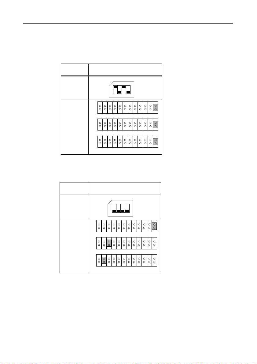
3. Hardware Setup
Names of Board Components
Figure 3.1. shows the names of various board components.
The switch and jumper settings shown in the figure are the default
factory settings.
Hardware Setup
Figure 3.1. Names of Board Components and Default
Factory Settings
COM-2(PC)F 23
Page 33

Hardware Setup
I/O Address Setting
The board is an I/O device controlled by I/O instructions from the
PC. I/O devices include expansion boards and devices inside the
PC. The various devices are identified by their I/O addresses.
I/O addresses are represented as four digit hexadecimal values
(e.g. 02A0H) and act as the ID number for each I/O device.
Most expansion boards are controlled via a range of consecutive I/O
addresses. The address of the first I/O address in the range is
called the base I/O address.
When using Enhanced mode, either 1A0H or 2A0H is selected as
the base I/O address. In Compatible mode, the fixed address for
the PC system is used.
Notes!
1. When using more than one expansion board, set each board so
that their I/O addresses do not overlap.
2. If the PC already has COM1 to COM4 ports, those ports cannot
be set for the board.
COM-2(PC)F24
Page 34

Setting Procedure
The I/O address is set using a DIP switch (SW1) on the board.
123
SW1
MODE
Figure 3.2. I/O Address DIP Switch
Table 3.1. I/O Address Settings
C
N
1
4
OFF
123
4
SW1 Interrupt Vector
Bit 1 Bit 2 Register Address
ON Enhanced 1A0~1A7 1BF
ON
OFF Enhanced 2A0~2A7 2BF
ON COM3 3E8~3EF ---
OFF
OFF COM1 3F8~3FF ---
I/O AddressFunction
Hardware Setup
SW1 Interrupt Vector
Bit 3 Bit 4 Register Address
ON Enhanced 1A8~1AF 1BF
ON
C
N
2
OFF Enhanced 2A8~2AF 2BF
ON COM4 2E8~2EF ---
OFF
OFF COM2 2F8~2FF ---
Function I/O Address
Figure 3.2 shows the CN1 bace I/O address set to 2A0H and the
CN2 bace I/O address set to 2A8H.
COM-2(PC)F 25
Page 35

Hardware Setup
Interrupt Level Setting
The signal from the LSI (NS16550 equivalent) on the board can be
used as an interrupt request signal based on the JP1, JP2, and JP3
settings.
Note!
When using interrupts, set an interrupt level that is not used by any
other device.
Setting Procedure
When not Using Interrupts
Place a short connector on the NC pin of each jumper (JP1, JP2, and
JP3).
When Using Interrupts
Connect the interrupt level using the short connector on each
jumper (JP1, JP2, and JP3). Available interrupt levels are IRQ3 to
7, 9 to 12, 14, and 15.
JP1
Enhanced
3 4 567 10 11
9
121415NC
Note!
JP2
COM CN1
COM CN2
3 4 5 6 7 10 11 121415NC
9
JP3
3 4 567 10 111214
9
15
NC
Figure 3.3. Interrupt Level Settings
If SW1 selects Enhanced mode, the settings in Figure 3.3. specify
that CN1 and CN2 both use IRQ5. If Compatible mode is set, the
settings specify that CN1 uses IRQ4 and CN2 uses IRQ3.
Jumper of the mode which isn’t used is to connect a short connector
to the NC pin.
COM-2(PC)F26
Page 36

Note!
Hardware Setup
Table 3.2. lists the I/O address and standard interrupt level settings
for COM1 to COM4 (Compatible mode).
Table 3.2. Example Compatible Mode Settings
Port I/O Address
COM1 3F8~3FF IRQ4
COM2 2F8~2FF IRQ3
COM3 3E8~3EF IRQ4 *1 *1 On the IBM PS/55Z and similar,
COM4 2E8~2EF IRQ3 COM3 uses IRQ3.
Interrupt Level
If using the PC's RS-232C ports as COM 1 and COM 2 at the same
time as using the CONTEC board as COM3 and COM4, COM3 and
COM4 must be set to interrupt levels other than IRQ3 and IRQ4
because COM1 uses IRQ4 and COM2 uses IRQ3.
COM-2(PC)F 27
Page 37

Hardware Setup
s
Mounting Method
There are many kinds of boards that can be mounted in a computer's
extension slots, however the mounting method is identical for any
slot.
Before starting
(1) Set the Power switch to OFF.
(2) Unplug the power cable from the AC outlet.
Mounting the board
(1) Remove the screws from the rear of the computer. When
removing screws, use a screwdriver that matches the screw
heads.
Cover mounting screws
Cover mounting screw
Figure 3.4. Rear Panel of IBM-PC/AT
(2) Hold the left and right sides of the front cover and remove it
from the computer's chassis by sliding it to the front.
Figure 3.5. Removing the Cover
COM-2(PC)F28
Page 38

Caution!
Hardware Setup
(3) Remove th e screw retaining the cover of the slot where the
board is to be mounted, and remove the cover from the rear
panel.
Figure 3.6. Expansion Slot Cover
To prevent a discharge of static electricity from damaging the board,
it is important to ground yourself. Hold the packaged board in
one hand and touch an unpainted, grounded metal surface with the
other hand. Then, hold the non-conductive part of the board and
remove it from the bag. Don't touch the underside side of the
board with the exposed pins and solder. Place the board on a
clean, non-conductive surface.
(4) Remove the board from the anti-static packaging.
(5) Inspect the board. Check the board for any visible damage or
loose parts. If you notice any problems with the board,
contact CONTEC. Don't attempt to fix the board yourself.
CONTEC does not warranty boards damaged or worked-on by
the customers.
(6) Insert the board into the expansion slot and press in firmly.
Make sure the board is fully seated in the support bracket.
COM-2(PC)F 29
Page 39

Hardware Setup
(7) Anchor the board with the screw. Use the screw set aside in
Figure 3.7. Anchoring the COM-2(PC)F
(8) Replace the computer cover.
(9) Connect the power cord.
step 3. Tighten so that the board is held in place.
COM-2(PC)F30
Page 40

Connecting the External Devices
Connecting the COM-2(PC)F board to external devices is via two
9-pin D-SUB connector (male) on the board.
Hardware Setup
5
CN1
1
5
CN2
1
On-board Connector : DELC-J9PAF-20L9 (Male) [mfd. by JAE]
Application Connector : 17JE-13090-02 (D8C) (Female) [mfd. by DDK]
9
6
9
6
Figure 3.8. Interface Connectors (CN1 and CN2)
(Signal Ground) SG
(Data Terminal Ready) DTR
(Transmit Data) TXD
(Receive Data) RXD
(Data Carrier Detect) DCD
5
9
4
8
3
7
2
6
1
CN1/CN2
RI (Ring Indicator)
CTS (Clear to Send)
RTS (Request to Send)
DSR (Data Set Ready)
Figure 3.9. CN1 and CN2 Pin Assignments
COM-2(PC)F 31
Page 41

Hardware Setup
Connecting the Cable
The RS-232C interface requires that you use a different type of
cable depending on the type of device being connected. For
example, modem connections and computer (PC) connections
require different cables. Accordingly, check the specifications of
the external device to which you are connecting and select the
appropriate type of cable. The two types of cable are "straightthrough" and "crossed". Also, if the signal lines require
conditioning in the connector, provide conditioning in accordance
with the specifications.
TXD
RXD
RTS
CTS
DTR
DSR
SG
Board
(Transmit Data)
TXD
(Receive Data)
RXD
RTS
(Request to Send)
(Clear to Send)
CTS
(Data Terminal Ready)
DTR
(Data Set Ready)
DSR
(Signal Ground)
SG
External Device
Figure 3.10. Example Connection to a Modem
TXD
RXD
RTS
CTS
DTR
DSR
SG
Board
TXD
RXD
RTS
CTS
DTR
DSR
SG
External Device
Figure 3.11. Example Connection to a PC
TXD
RXD
RTS
CTS
DTR
DSR
SG
Board
TXD
RXD
RTS
CTS
DTR
DSR
SG
External Device
Figure 3.12. Example Connection to a Device
COM-2(PC)F32
Page 42

4. System Reference
Specifications
Table 4.1. Specifications
Item Specification
Number of Channels 2
Input Type RS-232C
External connectors Two 9-pin D-SUB connector (Male)
Transfer Method Asychronous serial transfer
Baud Rate 50~115,200bps *1
Data Length
Parity heck Even, Odd, Non-parity *1
Controller Chip NS16550 or equivalent
Distance 15m Max.
Interrupt Requests
I/O Address 8 bits x 16 ports
Power Consumption +12VDC, 60mA Max.
Operating Temperature 0~50°C
Storage Temperature -20~60°C
Relative Humidity 20~90% non-condensing
Dimensions
Weight 130g
*1 : Software programmable.
For details, see "Appendix B Notes on Developing Driver Software" or refer to
the data sheet of the NS16550 or the equivalent chip.
5, 6, 7, 8 bits
1, 1.5, 2 stop bits *1
Enhanced mode : 1 level
Compatible mode : 2 levels
+5VDC, 420mA Max.
-12VDC, 50mA Max.
160.0 x 107.0 x 18.5mm
(6.3inch x 4.2inch x 0.7inch)
System Reference
Board Dimensions
160.0
107.0
[mm]
COM-2(PC)F 33
Page 43

System Reference
Circuitry Diagrams
SN75188
TXD, RTS, DTR
SN75189
15pF
Figure 4.1. Circuitry Diagrams
Block Diagram
The following is a block diagram of the COM-2(PC)F interface
board.
Addr. Bus
(A9~A3)
AEN
Addr. Bus
(A2~A0)
IOR
IOW
RESET
Data Bus
(D7~D0)
IBM-PC/AT BUS
RXD, CTS, DSR
ADDRESS
DECODER
CNTROL
BUFFER
DATA
BUFFER
INTERRUPT
VECTOR
REGISTER
CLOCK
NS16550
NS16550
RS-232C
DRIVER &
RECEIVER
RS-232C
DRIVER &
RECEIVER
CN1
Serial Port
CN2
Serial Port
IRQ3~7,
IRQ9~12,
IRQ14, 15
INTERRUPT
JUMPER
Figure 4.2. COM-2(PC)F Block Diagram
COM-2(PC)F34
COM-2(PC)F
Page 44

5. Troubleshooting
If you are having trouble with your board or program, answer the
following questions to see if you can find the problem.
QUESTIONS:
STEPS TO TAKE
Is the pilot light on?
The system must be turned on and the power supply must be
working. Check the main power switch and the power supply.
Did the system boot up?
If the board has been installed and the system did not boot, check
the following:
- Make sure the board has been inserted firmly. Pull it out and try
to reboot. If your system reboots, then re-insert the board and
try to boot again.
- Check that cables attached to your other boards fit tightly.
Troubleshooting
Does your program work?
If the system booted and your program does not work, check the
following:
- DIP switches have been set correctly for the desired base address.
- Selected base address doesn't conflict with another peripheral
device or card installed in the computer.
- Selected interrupt levels don't conflict with interrupts required by
other devices or cards.
- Try one of the sample programs provided on the disk and see if it
works.
COM-2(PC)F 35
Page 45

Troubleshooting
Does the sample program work?
Check the following:
- Signals are connected to the correct pins.
- Pin connections on the I/O cables are secure.
- Signals are present at the external connectors.
- Try using the COM-2(PC)F board with other non-essential boards
removed. Remove other boards one by one, checking the
COM-2(PC)F for successful operation after each board is
removed.
Is the input data accurate?
If you believe something is wrong with either the input data or the
output data, check the following:
- Environmental noise. Move the equipment and cables away
from sources of electrical noise. Try an isolated power source.
- Dirty connector edge. Clean the edge.
- External connectors fit tightly. Separate and reattach external
cables.
Still have a probrem?
Contact CONTEC group office where you purchased as shown in
the last page of this manual.
Note!
Before you call, make a list of the following information. Our
technical representatives will need the following information to help
you.
1. Your name, company, and phone number.
2. The brand and type of computer you are using (e.g. IBM-AT,
Compaq 386).
COM-2(PC)F36
Page 46

Troubleshooting
3. DOS Version.
4. Name of the CONTEC board that you are using.
5. Names of other boards in the computer.
6. I/O addresses for the CONTEC board and all other boards.
7. Interrupt levels for the CONTEC board and all other boards.
8. DMA channels for the CONTEC board and all other boards
(if applicable).
9. The programming language that you are using
(and the version number).
COM-2(PC)F 37
Page 47

Troubleshooting
10.Different I/O addresses you have tried.
11. Are you using your own program or a CONTEC sample
12.List AUTOEXEC.BAT.
13.List CONFIG.SYS.
program.
COM-2(PC)F38
Page 48

6. Appendix
A. Sample Programs (for MS-DOS)
This section covers the sample programs that are supplied on the
floppy disk included with this board.
COM-2(PC)F Diskette
CONTEC supplies a sample program diskette with each
COM-2(PC)F board. This diskette contains sample programs to
help you get started.
Use the DOS DIR command to see a list of files on the
COM-2(PC)F diskette.
A> dir
Backup Copy
Make a backup of the COM-2(PC)F diskette before use. This will
protect you if the original copy becomes damaged or destroyed.
Use the DOS DISKCOPY command.
A> diskcopy a: b:
Keep the original in a safe place and use the backup copy for the
following procedures.
Appendix
Copy Files to Hard Disk
If a hard disk drive is available on your PC, then installing and
executing the sample programs from the hard disk drive will be
faster than using a floppy drive. To run sample programs from the
hard drive, create a subdirectory named COM2F on your C drive
and copy the files from A: to C: with the following commands.
A:> c:
C:> md com2f
C:> xcopy A:¥*.* c:¥com2f /s
COM-2(PC)F 39
Page 49

Appendix
Sample Programs
The programs are written in GW-BASIC and Microsoft C.
The sample programs transmit data entered from the keyboard and
display received data on the screen. Table 6.1. lists the
communications data format.
The sample programs listed in Figure 6.1. are included on the
floppy disk.
Table 6.1. Data Format
Parameter Data Format
Data bits 8 bits
Stop bits 2 bits
Parity None
BAS
(1) H103HD01.BAS Data transmission (Enhanced mode)
(2) H103HD02.BAS Data reception (Enhanced mode)
(3) H103HD03.BAS Data transmission (COM1 mode)
(4) H103HD04.BAS Data reception (COM1 mode)
(5) H103HD05.BAS Data transmission and reception (Enhanced mode)
(6) H103HD06.BAS Data transmission and reception (COM1, COM2 mode)
(7) H103HD07.BAS Interrupt-driven data transmission and reception
H103HD.ASM
H103HD.BIN
(8) H103HD08.BAS Half-duplex data transmission (Enhanced mode)
(9) H103HD09.BAS Half-duplex data reception (Enhanced mode)
(10)COM21_1.C Data transmission and reception (COM1, COM2 mode)
MSC
COM2V
COM21_1.EXE
(11)COM34_1.C Data transmission and reception (COM3, COM4 mode)
COM34_1.EXE
SETCOM.EXE (Address setting file for Compatible mode)
Figure 6.1. Floppy Disk Files
COM-2(PC)F40
Page 50

Notes!
Appendix
- All the sample programs must be run on a PC operating under
MS-DOS.
- Sample programs 3, 4, 6, and 10 cannot be used on a PC that
already has COM1 and COM2 ports. Similarly, sample
programs 11 cannot be used on a PC that already has COM3 and
COM4 ports.
- As sample programs 8 and 9 use half-duplex mode, they can only
be used with the COM-2PD(PC) board.
COM-2(PC)F 41
Page 51
Appendix
Switch and Jumper Settings
Table 6.2. Switch and Jumper Settings of Sample Program 1,
2, and 5
Item
I/O Address
(SW1)
Interrupt Level
(JP1, JP2, JP3)
JP1
JP2
JP3
Settings
SW1
123
4
OFF
9 3 4 5 6 7 10 1112 1415 NC
9 3 4 5 6 7 10 1112 1415 NC
9 3 4 5 6 7 10 1112 1415 NC
Table 6.3. Switch and Jumper Settings of Sample Program 3,
4, 6, and 10
Item
I/O Address
(SW1)
Interrupt Level
(JP1, JP2, JP3)
JP1
JP2
JP3
Settings
SW1
123
4
OFF
9 3 4 5 6 7 10 1112 1415 NC
9 3 4 5 6 7 10 1112 1415 NC
9 3 4 5 6 7 10 1112 1415 NC
COM-2(PC)F42
Page 52

Appendix
Table 6.4. Switch and Jumper Settings of Sample Program 7
Item
I/O Address
(SW1)
Interrupt Level
(JP1, JP2, JP3)
JP1
JP2
JP3
Settings
SW1
123
4
OFF
9 3 4 5 6 7 10 1112 14 15 N C
9 3 4 5 6 7 10 1112 14 15 N C
9 3 4 5 6 7 10 1112 14 15 N C
Table 6.5. Switch and Jumper Settings of Sample Program 11
Item
I/O Address
(SW1)
Interrupt Level
(JP1, JP2, JP3)
JP1
JP2
JP3
Settings
SW1
123
4
OFF
9 3 4 5 6 7 10 1112 1415 NC
9 3 4 5 6 7 10 1112 1415 NC
9 3 4 5 6 7 10 1112 1415 NC
COM-2(PC)F 43
Page 53

Appendix
Cable Connection
When running the sample programs 1 to 11 (except 8 and 9), use the
interconnection cable as shown in Figure 6.2. for connection with
the mating device in the Compatible mode. For use in the
Enhanced mode, on the other hand, use the cross cable or the
interconnection configuration diagram in Figure 6.2.
Signal
Pin No.
3
TXD
2
RXD
4
DTR
6
DSR
5
SG
1
DCD
7
RTS
8
CTS
CH1 External device or CH2
Pin No. Signal
2
RXD
TXD
3
6
DSR
4
DTR
SG
5
RTS
7
8
CTS
DCD
1
Figure 6.2. 9-pin Connector Diagram
COM-2(PC)F44
Page 54

Appendix
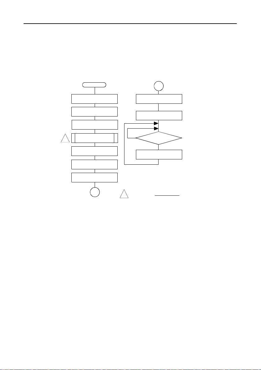
Sample Program 1
This GW-BASIC sample program demonstrates the transmit-data
capability of COM-2(PC)F in Enhanced mode. First, it initializes
the Asynchronous Communication Element (ACE), then it
transmits the data input from the keyboard to the external device
through channel 1 (CN1).
START
Set Baud Rate
Generator
Interrupt Enable Register
Set Transmission Format
1
Set
(Line Control Register)
Wait Time
(After Initialization)
Set Modem Control
Output
Read
Line Status Register
Read
Received Data Register
1
Note:
1
Modem Status Register
None Key
No
Wait Time =
1
Read
Interrupt ID Register
Read
A$=INKEY$
In Key
Line Status
D5 bit = 1
Yes
Data Transmission
Data Length
Baud Rate
Figure 6.3. Flowchart of Sample Program 1
(sec)
COM-2(PC)F 45
Page 55
Appendix
Sample Program 2
This GW-BASIC sample program demonstrates the receive-data
capability of COM-2(PC)F in Enhanced mode. First, it initializes
the ACE, then it transmits the data input from the external device to
CRT through CN1.
START
Set Baud Rate
Generator
Interrupt Enable Register
Set Transmission Format
1
Set
(Line Control Register)
Wait Time
(After Initialization)
Set Modem Control
Output
Read
Line Status Register
Read
Received Data Register
1
Note:
Modem Status Register
No
Display Receiver Buffer's
1
Wait Time =
1
Read
Interrupt ID Register
Read
Line Status
D0 bit = 1
Yes
Data On CRT
Data Length
Baud Rate
Figure 6.4. Flowchart of Sample Program 2
(sec)
COM-2(PC)F46
Page 56

Appendix
Sample Program 3
This GW-BASIC sample program demonstrates the transmit-data
capability of COM-2(PC)F in Compatible mode. Using this
[OPEN "COM1 : 9600, N, 8, 2, DS" AS #1] command opens the
RS-232C communication file (COM1). It then writes the data
input from the keyboard to COM1 through CN1.
START
Set
Communication File
None Key
A$=INKEY$
In Key
Data Transmission
Figure 6.5. Flowchart of Sample Program 3
COM-2(PC)F 47
Page 57

Appendix
Sample Program 4
This GW-BASIC sample program demonstrates the receive-data
capability of COM-2(PC)F in Compatible mode. Using this
[OPEN "COM1 : 9600, N, 8, 2, DS" AS #1] command opens the
RS-232C communication file (COM1). It then reads the data from
COM1 and outputs to CRT through CN1.
START
Set
Communication File
Yes
File Buffer = 0
No
Display File Buffer's
Data On CRT
Figure 6.6. Flowchart of Sample Program 4
COM-2(PC)F48
Page 58

Appendix
Sample Program 5
This GW-BASIC sample program demonstrates the
receive/transmit-data capability of COM-2(PC)F in Enhanced mode.
First, it initializes the ACE, it then receives the data input from the
keyboard through CN1. Finally it outputs the data to CRT through
CN2.
START
Channel 1
Set Baud Rate
Generator
Interrupt Enable Register
Set Transmission Format
1
Set
(Line Control Register)
Wait Time
(After Initialization)
Set Modem Control
Output
Read
Line Status Register
Read
Received Data Register
Read
Interrupt ID Register
Read
Modem Status Register
1
Channel 2
Interrupt Enable Register
Set Transmission Format
(Line Control Register)
1
Received Data Register
Modem Status Register
1
Set Baud Rate
Generator
Set
Wait Time
(After Initialization)
Set Modem Control
Output
Read
Line Status Register
Read
Read
Interrupt ID Register
Read
2
Note:
Figure 6.7. Flowchart of Sample Program 5
1
None Key
Wait Time =
A$=INKEY$
Line Status
D5 bit = 1
No
Data Transmission
Line Status
D0 bit = 1
No
Display File Buffer's Data
On CRT
Data Length
Baud Rate
2
In Key
Yes
Yes
(sec)
COM-2(PC)F 49
Page 59

Appendix
Sample Program 6
This GW-BASIC sample program demonstrates the
receive/transmit-data capability of COM-2(PC)F in Compatible
mode. Using the [OPEN "COM1 : 9600, N, 8, 2, DS" AS #1]
command and the [OPEN "COM2 : 9600, N, 8, 2, DS" AS #2]
command opens two RS-232C communication files (COM1 and
COM2). The program sends the keyboard input data from COM1
to COM2 and displays the data received from COM2 to CRT.
START
Set COM1
Set COM2
None Key
A$=INKEY$
In Key
Data Transmission
File Buffer = 0
Yes
Display File Buffer's Data
No
On CRT
Figure 6.8. Flowchart of Sample Program 6
COM-2(PC)F50
Page 60

Appendix
Sample Program 7
This GW-BASIC sample program demonstrates the
receive/transmit-data capability of COM-2(PC)F in Enhanced mode
with interrupt input. It calls a machine language program to
register and handle interrupt input. One channel's receive/transitdata routine is processed in the interrupt handler. The received
data is stored in the data buffer. Data to be transmitted is read
from the data buffer.
START
Register
Machine Language Area
Set Segment
Load Interrupt
Handling Program
Set Baud Rate
Generator
Interrupt Enable Register
Set Transmission Format
1
Set
(Line Control Register)
Wait Time
(After Initialization)
Set Modem Control
Output
Read
Line Status Register
Read
Received Data Register
Read
Interrupt ID Register
Read
Modem Status Register
Interrupt Control Port
D7 bit ON
1
Note:
1
No
Data Transmission
No
Wait Time =
1
A$=INKEY$
In Key
Line Status
D5 bit = 1
Yes
Line Status
D0 bit = 1
Yes
Receive Data
Data Length
Baud Rate
None Key
(sec)
Figure 6.9. Flowchart of Sample Program 7
COM-2(PC)F 51
Page 61

Appendix
Sample Program 8
[Half-duplex data transmission (Enhanced mode)]
The sample program 8 enables initialization on ACE, data
transmission in the transmission mode, and waits for the receive
data in the receive mode.
START
Set Baud Rate
Note:
Generator
Set Interrupt Enable
Register
Set Transmission Format
(Line Control Register)
1
1
WAIT Time
(After Initialization)
Set Modem
Control Output
Read
Line Status Register
Read
Received Data Register
Read
Interrupt ID Register
Read
Modem Status register
Modem Control
RTS to LOW
Wait Time =
1
Data Length
Baud Rate
No
No
(sec)
Line Status
D6 bit = 1
Data Transmission
5 bytes Tramsmit
No
Transmit end
Modem Control
RTS to High
Line Status
No
No
D0 bit = 1
Display Receiver Buffer's
Data 0n CRT
5 bytes Receive
END
Figure 6.10. Flowchart of Sample Program 8
1
Yes
Yes
Yes
Yes
Yes
COM-2(PC)F52
Page 62

Appendix
Sample Program 9
[Half-duplex data reception (Enhanced mode)]
The sample program 9 enables initialization on ACE, receives
5-byte data; after transmission, the program enters the transmission
mode for data transmission.
Note:
START
Set Baud Rate
Generator
Set Interrupt Enable
Register
Set Transmission Format
(Line Control Register)
1
1
WAIT Time
(After Initialization)
Set Modem
Control Output
Line Status Register
Received Data Register
Interrupt ID Register
Modem Status Register
Wait Time =
Read
Read
Read
Read
1
Data Length
Baud Rate
(sec)
1
Line Status
No
No
No
No
No
D0 bit = 1
Display Receiver Buffer's
Yes
Data 0n CRT
5 bytes Receive
Yes
Modem Control
RTS to LOW
Line Status
D6 bit = 1
Yes
Data Transmittion
5 bytes Transmit
Yes
Transmit end
Yes
Modem Control
RTS to High
END
Figure 6.11. Flowchart of Sample Program 9
COM-2(PC)F 53
Page 63

Appendix
Sample Program 10
[Data transmission and reception (COM1, COM2 mode)]
Sample program 10 uses the bios_serialcom( ) function for MS-C.
It first receives the data transmitted from COM1, and then receives
the data at COM1 transmitted from COM2. Received data is
displayed on the CRT.
START
COM1
Initialization
COM2
Initialization
Transmit 1-byte
Data from COM1
COM2 status check
ready to receive?
No
COM2
Data Reception
Data reception A to K
from COM1 completed?
No
No
Yes
from COM2 completed?
No
Yes
1
1
COM1
Initialization
COM2
Initialization
Transmit 1-byte
Data from COM2
COM1 status check
ready to receive?
Yes
COM1
Data Reception
Data reception a to k
Yes
END
Figure 6.12. Flowchart of Sample Program10
COM-2(PC)F54
Page 64

Appendix
Sample Program 11
[Data transmission and reception (COM3, COM4 mode)]
Sample program 11 uses the bios_serialcom( ) function for MS-C.
It first receives the data transmitted from COM3, and then receives
the data at COM3 transmitted from COM4. Received data is
displayed on the CRT.
START
COM3
Initialization
COM4
Initialization
Transmit 1-byte
Data from COM3
COM4 status check
ready to receive?
No
COM4
Data Reception
Data reception A to K
from COM3 completed?
No
No
Yes
from COM4 completed?
No
Yes
1
1
COM3
Initialization
COM4
Initialization
Transmit 1-byte
Data from COM4
COM3 status check
ready to receive?
Yes
COM3
Data Reception
Data reception a to k
Yes
END
Figure 6.13. Flowchart of Sample Program 11
COM-2(PC)F 55
Page 65

Appendix
B. Notes on Developing Driver Software
Internal Registers
COM-2(PC)F uses the NS16550 (National Semiconductor) as the
Asynchronous Communication Element (ACE). Within the
address range of each channel, the offset addresses 0 through 7
furnish access to the internal registers of each of the two ACE's.
Table 6.6. shows how functions relate to the internal registers. To
access the baud rate generator (defined on the next page), the
DLAB signal must be set high. For more details on NS16550,
refer to the National Semiconductor Data Book.
Table 6.6. Function Selection through Internal Registers
I/O Port Address DLAB *1 ACE Register (NS16550) Note *2
"Base Address" +0H 0 Receiver (Buffer register) R
"Base Address" +0H 0 Transmitter (Holding register) W
"Base Address" +1H 0 Interrupt Enable Register
"Base Address" +2H x Interrupt ID R
"Base Address" +2H x FIFO Control W
"Base Address" +3H x Line Control
"Base Address" +4H x Modem Control
"Base Address" +5H x Line Status
"Base Address" +6H x Modem Status
"Base Address" +7H x Scratchpad Register
"Base Address" +0H 1 Baud Rate Divider Register LSB
"Base Address" +1H 1 Baud Rate Divider Register MSB
*1 DLAB: Divisor Latch Access Bit in the Modem Status Register.
*2 R=Read only; W=Write only.
COM-2(PC)F56
Page 66

Baud Rate Selection
The COM-2(PC)F board has one programmable baud rate generator
for each of the two ACEs. The ACEs use a 1.8432MHz crystal
oscillator as clock input. The baud rate generator takes the
1.8432MHz clock and divides it by a divisor from 1 to (216 - 1).
The output frequency of the baud rate generator equals 16 times the
baud rate.
Based on the originating clock frequency, the baud rate is derived
as:
Divisor = clock frequency/(baud rate x 16)
Two eight-bit divisor registers on the ACEs store the divisor in a
16-bit binary format. These divisors must be loaded during
initialization into Divider registers (see Table 6.6.). Table 6.7.
provides frequently used baud rates and their divisors. The
percent error is the difference between actual and desired value.
Table 6.7. Baud Rate and Divisors
Desired Baud Rate Divisor Percent Error
50 2304 --75 1536 ---
110 1047 0.026
134.5 857 0.058
150 768 --300 384 --600 192 ---
1200 96 --1800 64 --2000 58 0.680
2400 48 --3600 32 --4800 24 --7200 16 ---
9600 12 --19200 6 --38400 3 --57600 2 ---
115200 1 ---
Appendix
COM-2(PC)F 57
Page 67

Appendix
LSI Recovery Time
Due to the ever higher CPU clock rates used in PCs, restrictions
apply when controlling a peripheral LSI device by software.
Table 6.8. lists the LSIs used on CONTEC boards which require
special consideration when accessing. Take note of the following
point when accessing these LSIs.
In PCs using i386 or earlier CPUs, software waits (JMP $+2) can be
used to provide a recovery time when accessing the LSI. However,
software waits cannot be used to provide a recovery time in PCs
with a i486 or later CPU because of the CPU cache memory
function.
The following describes one method of providing the recovery time
when using an i486 or later CPU.
In the PC/AT and compatible computers, executing an IN
instruction for the port at I/O address 2EFh (COM4 scratch register)
takes a minimum of 0.5µs. As this time does not depend on the
CPU type or clock rate, the time can be used to provide the
recovery time. After accessing any of the devices listed in
Table 6.8., execute the IN instruction for the 2EFh port the required
number of times to provide the recovery time.
Table 6.8. Number of Times the IN Instruction Must be
Executed for the 2EFh Port after Accessing the LSI
LSI Device Output Input
i8237 or equivalent None None
i8254 or equivalent Once Once
i8255 or equivalent Once Once
i8259 or equivalent Once Once
NS16550 or equivalent Once Once
PD7210C Once None
µ
COM-2(PC)F58
Page 68

Appendix
Example program (for accessing an i8254 or equivalent)
- Microsoft Macro Assembler
OUT DX, AL ; Access to the i8254
IN AL, 2EFH ; Execute IN AL, 2EFH once to provide
the recovery time
- Microsoft C/C++
outp(port, byte); /* Access to the i8254 */
rt=inp(0x2ef); /* Execute rt=inp(0x2ef); once to
provide the recovery time */
COM-2(PC)F 59
Page 69

Appendix
Various Aspects of Interrupt Handling in Enhanced Mode
and Compatible Mode
Enhanced Mode
When in Enhanced mode, two channels of the COM-2(PC)F share
the same interrupt request line. The interrupt levels can be set
from IRQ3~IRQ7, IRQ9~IRQ12, IRQ14, and IRQ15 by setting JP1
before installing this board. Each channel's interrupt signal will be
latched in the Interrupt Vector Register (IVR).
Therefore, when the CPU receives an interrupt requirement, the
interrupt service routine can check the IVR to determine which
channel is requesting interrupt service. After finishing the
interrupt service process, the interrupt service routine has to check
IVR again to see if a Pending interrupt request has occurred.
ACE (Asynchronous Communication Element) has its own internal
register for enabling interrupts and identifying the interrupt service
requesting channel. Refer to National Semiconductor's data book
for additional details on NS16550 and its operation.
When turning on the PC's main power, the ACE's master reset
function sets OUT1 to "High". This status automatically enables
the interrupt. If one of the two channels is not allowed to generate
the interrupt, set the OUT1 bit to "Low".
In addition to being able to enable/disable interrupt by channel, the
board also has a global interrupt enable function. This global
interrupt enable function determines whether the IRQ line is active
or not. When turning on the power, this function sets to the
disable status. To enable the PC bus to accept an interrupt, this
function has to be programmed to enable status. To enable this
function, write "1" to IVR's D7 bit; to disable this function, write
"0" to IVR's D7 bit.
Figure 6.14. describes the bit function of IVR in Enhanced mode.
The I/O address of IVR is either 2BF or 1BF.
COM-2(PC)F60
Page 70

Appendix
Output Port
D7
2BF/1BF
Input Port
2BF/1BF
D6 D5 D4 D3 D2 D1 D0
Not Used
D7
D6 D5 D4 D3 D2 D1 D0
Not Used
Global Interrupt
0: Disable
1: Enable
CH1 Interrupt
0: Occurred
1: Not Occurred
CH2 Interrupt
0: Occurred
1: Not Occurred
Global Interrupt
0: Enable
1: Disable
Figure 6.14. IVR Bit Function in Enhanced Mode
Compatible Mode
When in the Compatible mode, CN1 of the interface board is
compatible with COM1 or COM3 and CN2 is compatible with
COM2 or COM4. By using JP2 and JP3, interrupt levels can be
selected from IRQ3~IRQ7, IRQ9~IRQ12, IRQ14, and IRQ15 for
CN1 and CN2. Normally, COM1/COM3 uses IRQ4 and
COM2/COM4 uses IRQ3.
COM-2(PC)F 61
Page 71

Appendix
C. The Details on NS16550
Table 6.9. NS16550's Register
(Short from National Semiconductor's data book)
< 1 / 2 >
0 DLAB = 0 0 DLAB = 0 1 DLAB = 0 2 2 3
Bit Receiver Transmitter Interrupt Interrupt FIFO Line
No. Buffer Holding Enable Ident. Control Control
Register Register Register Register Register Register
(Read Only) (Write Only) (Read Only) (Write Only)
RBR THR IER IIR FCR LCR
0 Data Bit 0 Data Bit 0 Enable "0" if FIFO Word
Received Interrupt Enable Length
Data Pending Select
Available Bit 0
Interrupt (WLS0)
(ERBFI)
1 Data Bit 1 Data Bit 1 Enable Interrupt RCVR Word
Transmitter ID FIFO Length
Holding Bit (0) Reset Select
Register Bit 1
Empty (WLS1)
Interrupt
(ETBEI)
2 Data Bit 2 Data Bit 2 Enable Interrupt XMIT Number of
Receiver ID FIFO Stop Bits
Line Status Bit (1) Reset (STB)
Interrupt
(ELSI)
3 Data Bit 3 Data Bit 3 Enable Interrupt DMA Parity
MODEM ID Mode Enable
Status Bit (2) Select (PEN)
Interrupt
(EDSSI)
4 Data Bit 4 Data Bit 4 0 0 Reserved Even
5 Data Bit 5 Data Bit 5 0 0 Reserved Stick
Register
Parity
Select
(EPS)
Parity
6 Data Bit 6 Data Bit 6 0 FIFOs RCVR Set
7 Data Bit 7 Data Bit 7 0 FIFOs RCVR Divisor
Enabled Trigger Break
(LSB)
Enabled Trigger Latch
(MSB) Access Bit
(DLAB)
COM-2(PC)F62
Page 72

Table 6.9. NS16550's Register
(Short from National Semiconductor's data book)
< 2 / 2 >
Register
4 5 6 7 0 DLAB = 1 1 DLAB =1
Bit MODEM Line MODEM Scratch Divisor Divisor
No. Control Status Status Register Latch Latch
Register Register Register (LS) (MS)
MCR LSR MSR SCR DLL DLM
0 Data Data Delta Bit 0 Bit 0 Bit 8
Terminal Ready Clear
Ready (DR) to Send
(DTR) (DCTS)
1 Request Overrun Delta Bit 1 Bit 1 Bit 9
to Send Error Data
(RTS) (OE) Set Ready
(DDSR)
Appendix
2 Out 1 Parity Trailing Bit 2 Bit 2 Bit 10
3 Out 2 Framing Delta Bit 3 Bit 3 Bit 11
4 Loop Break Clear Bit 4 Bit 4 Bit 12
5 0 Transmitter Data Bit 5 Bit 5 Bit 13
6 0 Transmitter Ring Bit 6 Bit 6 Bit 14
7 0 Error in Data Bit 7 Bit 7 Bit 15
Error Edge Ring
(PE) Indicator
(TERI)
Error Data
(FE) Carrier
Detect
(DDCD)
Interrupt to Send
(BI) (CTS)
Holding Set
Register Ready
(THRE) (DSR)
Empty Indicator
(TEMT) (RI)
RCVR Carrier
FIFO Detect
(DCD)
COM-2(PC)F 63
Page 73

Appendix
D. Difference Between the COM-2(PC)F
and COM-2(PC)V
The COM-2(PC)F is an upgrade of the previous COM-2(PC)V
board and is upwardly compatible. Therefore, the board can
generally be used in the same way as the COM-2(PC)V.
However, as the bus specification has changed from the XT bus to
the AT bus and the board sizes are different, the COM-2(PC)F may
not fit in some PCs. Check the size of board that can be mounted
in your PC before selecting the COM-2(PC)F. The two boards
also differ in their specifications and hardware setup. The
differences are described below.
Table 6.10. Specifications Differences
COM-2(PC)V COM-2(PC)F
Bus XT Bus AT Bus
Baud Rate 50~38,400bps 50~115,200bps
Interrupt Level IRQ3~7, 9 IRQ3~7, 9~12, 14, 15
(Jumper Selectable) (Jumper Selectable)
Dimensions 120.0 x 107.0 x 18.5mm 160.0 x 107.0 x 18.5mm
Interrupt
setting
COM-2(PC)V
JP1~JP3
4 5 6
2 3
(Jumper Selectable)
7
NC
COM-2(PC)F
JP1~JP3
(Jumper Selectable)
Figure 6.15. Difference in Jumpers (JP1~JP3)
COM-2(PC)F64
NC9 3 4 567 1011 121415
Page 74

7. Index
Index
B
Baud Rate, 57
Block Diagram, 34
Board Setup, 25
C
Circuitry Diagrams, 34
Compatible Mode, 5
Connectors, 31
E
Enhanced Mode, 5
External Connection, 31
F
Features, 1
M
Mounting Method, 28
MS-DOS, 20
N
NS16550's Register, 62
O
Obtain Service, 2
S
Sample Programs, 39
Setup, 23
Specifications, 33
Support Software of Option, 1
System Reference, 33
I
I/O Address, 24
Internal Registers, 56
Interrupt Level, 26
L
Liability, 2
LSI Recovery Time, 58
T
Troubleshooting, 35
COM-2(PC)F 65
Page 75

Index
W
Warranty, 2
Windows 2000, 14
Windows 3.1, 19
Windows 95, 10
Windows Me/98, 6
Windows NT, 18
COM-2(PC)F66
Page 76

A-41-606
021025 [961015]
LZU2821
Page 77

CONTEC Group
JAPAN : Headquarters
CONTEC Co., LTD.
3-9-31, Himesato, Nishiyodogawa-ku, Osaka 555-0025, Japan
Tel : +81 (6) 6477-5219 Fax : +81 (6) 6477-1692
E-mail : intsales@osaka.contec.co.jp
U.S.A. : CONTEC MICROELECTRONICS U.S.A. INC.
744 South Hillview Drive, Milpitas, CA 95035 U.S.A.
Tel : +1 (408) 719-8200 Fax : +1 (408) 719-6750
E-mail : tech_support@contecusa.com
EUROPE : CONTEC MICROELECTRONICS EUROPE B.V.
Binnenweg 4, 2132 CT, Hoofddorp, The Netherlands
Tel : +31 (23) 567-3030 Fax : +31 (23) 567-3035
E-mail : tech_support@conteceu.nl
KOREA : HYOJIN CONTEC Co., LTD.
Ki-im Bldg. #399, Shindolim-Dong, Kuro-ku, Seoul, Korea
Tel : +82 (2) 2636-4277/8 Fax : +82 (2) 2636-4279
E-mail : product@conteck.com
CHINA : INTERNATIONAL CONTEC TECHNOLOGY CO., LTD.
B-8F, Hua Tong Building, No. B19, Che Gong Zhuang West Road,
Hai Dian District, Beijing 100044, China
Tel : +86(10)8801-8228 Fax : +86 (10)8801-8209
E-mail : ict@ict.com.cn
SHANGHAI CONTEC MICROELECTRONICS CORP.
No. 481 Gui Ping Road, Cao He Jing Hi-Tech Park Shanghai, 200233, China
Tel : +86 (21) 6485-1907 Fax : +86 (21) 6485-0330
E-mail : contec@contec.com.cn
SHENYANG CONTEC MICROELECTRONICS Co., LTD.
No. 169, Qingnian Street, Shenhe District, Shenyang 110015, China
Tel : +86 (24) 2392-9771 Fax : +86 (24) 2392-9773
TAIWAN : MACROMATE CORP.
8F, Universal Center, No.179, Ta-Tung Rd., Sec.1 Hsi-Chih, Taipei Hsien, Taiwan,
R.O.C
Tel : +886 (2) 2647-9353 Fax : +886 (2) 2647-9373
E-mail : intl@macromate.com.tw
A-46-368 Ver. 2001. 02. 06
 Loading...