

Page 1

AlphaServer DS20
Service Manual
Order Number: EK–AS140–SV. A 01
This manual is for anyone who services this system. It includes
troubleshooting information, configuration rules, and instructions for
removal and replacement of field-replaceable units.
Compaq Computer Corporat ion
Page 2

Notice
The in fo rmatio n in this p ublication is subject to ch ange w ithout n otice.
COMPAQ COMPUTER CORPORATION SHALL NOT BE LIABLE FOR TECHNICAL
OR EDITORIAL ERRORS OR OMISSIONS CONTAINED HEREIN, NOR FOR
INCIDENTAL OR CONSEQUENTIAL DAMAGES RESULTING FROM THE
FURNISHING, PERFORMANCE, OR USE OF THIS MATERIAL.
This publication c ont ai ns in formation protecte d by copyright. No par t of this p ubl ic at ion may b e
photocopied or repr oduced in any form without prior written consent from Compaq Co mp ut er
Corporation.
The software desc ri bed i n th is do cument is furnished under a license agreement or
nondisclosure agr eement and may be used or copied only in acco rda nce with the terms of the
agreement.
© 1999 Digital Equipment Corporat ion.
All rights res e rved. P rinted in the U. S .A.
COMPAQ and the Compaq logo are trademarks or registere d tr adem arks of Compaq Computer
Corporation. A lphaS erver, DIGITAL, OpenVMS, and StorageWorks are trademarks or
registered trademarks of Digital Equ ip me nt Corporation. Micros oft, Windows, and Windows
NT are registere d tr ademarks of Microsoft Corporat ion. U N IX is a regi stered tradem ar k in th e
U.S. and other countr ie s, licens ed exclusively through X/Open Company Ltd. Other produc t
names mentioned herein may be trademarks and/o r reg is tered trademarks of their respect iv e
companies.
Digital Equipmen t Corporation now ow ned by C ompaq Compu ter Co rporation.
FCC Notice: The equipment described in thi s ma nual generates, use s, and may emit radio
frequency energ y. T he equipment has been typ e te st ed and f ound to comply with the l im i ts for a
Class A digital device pursuant to Part 15 of FCC Rules, w hich are de si gned to provide
reasonable prote ct ion a gainst such radio freq uency interferenc e. O pera ti on of thi s equ ipment in
a residential area may cause inter fe rence, in which case the user at his own expense will be
required to take w hat ever measures a re re quired to correc t the interference.
Shielded Cables: If shielded cables have been supplied or specified, they mus t be us ed on t he
syste m in order to mainta in internatio n al regulatory compliance.
Warning! This is a Clas s A produ ct. In a do mestic environment this product may cause radio
interference, in wh i ch case the user may be required to take adequate measures.
Achtung! Dieses ist ein Gerä t de r Funk st örgrenzwertkla ss e A . In Wohnbereichen können bei
Betrieb dieses Geräte s Rundfunkstörungen auftreten, in welchen Fäl le n der Be nut zer für
entsprechend e G egenmaßnahmen ve rantwortlich ist.
Avertissement! Cet appareil est un appareil de Classe A. Dans un environnement résidentiel,
cet appareil peut provoquer des brouillages radioélectriques. Dans ce cas, il peut être demandé à
l'utilisateur de prendre les mesures appropriées.
Page 3

Contents
Preface ........................................................................... ix
Chapter 1 System Overview
1.1 System Enclosure.....................................................................................1-2
1.2 Operator Control Panel and Drives........................................................... 1-4
1.3 System Consoles ......................................................................................1-6
1.4 System Architecture................................................................................. 1-8
1.5 CPU Types.............................................................................................1-10
1.6 Memory .................................................................................................1-12
1.7 Memory Addressing and Data Location ..................................................1-14
1.8 System Board.........................................................................................1-16
1.8.1 Cross-Bar Switch and System Components ......................................1-18
1.8.2 I/O Subsystem.................................................................................1-20
1.8.3 System Board Switchpacks..............................................................1-22
1.9 Server Feature Module...........................................................................1-24
1.9.1 Power Control Logic .......................................................................1-26
1.10 Power C ir cuit and C o ver Interlock..........................................................1-28
1.11 Power Supply.........................................................................................1-30
1.12 Power Up/Down Sequence.....................................................................1-32
1.13 TIG Bus.................................................................................................1-34
1.14 Maintenance Bus (I
1.15 StorageWorks Drives.............................................................................. 1-38
2
C Bus).....................................................................1-36
Chapter 2 Troubleshooting
2.1 Troubleshooting During Power-Up...........................................................2-2
2.2 Control Panel Display and Troubleshooting..............................................2-4
2.3 Power-Up Display and Troubleshooting....................................................2-6
2.4 Running Diagnostics — Test Command ...................................................2-8
2.5 Testing an Entire System..........................................................................2-9
2.6 Other Useful Console Commands...........................................................2-11
2.7 Troubleshooting with LEDs....................................................................2-12
2.8 Compaq Analyze....................................................................................2-14
2.8.1 Compaq Analyze Graphics Interface (GUI)......................................2-14
2.8.2 Description of the Error...................................................................2-16
2.9 Releasing Secure Mode..........................................................................2-20
iii
Page 4

Chapter 3 Error Registers
3.1 Ibox Status Register - I_STAT..................................................................3-2
3.2 Memory Management Status Register – MM_STAT.................................3-3
3.3 Dcache Status Register – DC_STAT.........................................................3-5
3.4 Cbox Read Register..................................................................................3-7
3.5 Miscellaneous Register (MISC) ................................................................3-9
3.6 Device Interrupt Request Register (DIRn, n=0,1).................................... 3-12
3.7 Pchip Error Register (PERROR).............................................................3-13
3.8 Failure Register......................................................................................3-16
3.9 Funct i o n R egiste r...................................................................................3-18
Chapter 4 Removal and Replacement
4.1 System Safety.......................................................................................... 4-1
4.2 FRU List..................................................................................................4-2
4.3 System Access .........................................................................................4-6
4.4 CPU Removal and Replacement............................................................... 4-8
4.5 Memory Module Removal and Replacement..................................4-10
4.6 System Board Removal and Replacement...............................................4-12
4.7 PCI/ISA Option Removal and Replacement ............................................4-14
4.8 Server Feature Module Removal and Replacement..................................4-16
4.9 Power Supply Removal and Replacement............................................... 4-18
4.10 Power Harness Removal and Replacement..............................................4-20
4.11 Power Transition Module Removal and Replacement..............................4-22
4.12 Auxiliary Fan Removal and Replacement...............................................4-24
4.13 System Fan Removal and Replacement...................................................4-26
4.14 Cover Interlock Removal and Replacement............................................. 4-28
4.15 Operator Control Panel Removal and Replacement................................4-30
4.16 CD-ROM Removal and Replacement..................................................... 4-32
4.17 Floppy Removal and Replacement..........................................................4-34
4.18 SCSI Disk Removal and Replacement....................................................4-36
4.19 StorageWorks Backplane Removal and Replacement..............................4-38
4.20 StorageWorks UltraSCSI Bus Extender Removal and Replacement.........4-40
Appendix A Halts, Console Commands, and Environment
Variables
A.1 Halt Button Functions..............................................................................A-2
A.2 Using the Halt Button..............................................................................A-3
A.3 Ha lt Assertion .........................................................................................A-4
A.4 Summary of SRM Console Commands....................................................A-6
A.5 Summary of SRM Environment Variables...............................................A-8
A.6 Recordi n g Envir o n ment Va r iables.........................................................A-10
iv
Page 5

Appendix B Managing the System Remotely
B.1 RCM Overview.......................................................................................B-2
B.2 First-Time Setup.....................................................................................B-3
B.2.1 Using RCM Locally or with a Modem on COM1...............................B-4
B.3 RCM Commands.....................................................................................B-5
B.4 Using the RCM Switchpack...................................................................B-10
B.5 Troubleshooting Guide..........................................................................B-13
Appendix C Firmware Update
C.1 Updating Firmware and Consoles............................................................C-2
C.1.1 Updating Firmware from the CD-ROM....................................................C-4
C.1.2 Updating Firmware from Floppy Disk — Creating th e Diskettes.............. C-8
C.1.3 Updating Firmware from Floppy Disk — Performing the Update........... C-10
C.1.4 Updating Firmware from a Network Device........................................... C-14
C.1.5 LFU Commands.................................................................................... C-18
Examples
1–1 Show Memory............................................................................................1-15
2–1 Power-Up Display........................................................................................2-6
2–2 Test Command Syntax..................................................................................2-8
2–3 Sample Test Command.................................................................................2-9
2–4 Show Power............................................................................................... 2-11
2–5 Show Memory............................................................................................2-11
2–6 Compaq Analyze Error Report....................................................................2-16
2–7 Releasing/Reestablishing Secure Mode.......................................................2-20
B–1 Invoking and Leaving RCM Locally ............................................................ B-4
C–1 Starting LFU from the SRM Console ........................................................... C-2
C–2 Booting LFU from the CD-ROM ................................................................. C-3
C–3 Updating Firmware from the CD-ROM ........................................................ C-4
C–4 Creating Update Diskettes on an OpenVMS System..................................... C-9
C–5 Updating Firmware from the Floppy Disk .................................................. C-10
C–6 Selecting AS1400FW to Update Firmware from the Internal Floppy Disk . . . C-13
C–7 Updating Firmware from a Network Device............................................... C-14
v
Page 6

Figures
1-1 System Enclosure.........................................................................................1-2
1-2 Cover Interlock Circuit.................................................................................1-3
1-3 Control Panel Assembly...............................................................................1-4
1-4 Block Diagram.............................................................................................1-8
1-5 CPU Module Placement .............................................................................1-10
1-6 Memory Placement.................................................................................... 1-12
1-7 Contents of DIMMs ................................................................................... 1-14
1-8 Memory Configuration...............................................................................1-15
1-9 System Board.............................................................................................1-16
1-10 Cross-Bar Switch Data Block Diagram .......................................................1-18
1-11 PCI Block Diagram....................................................................................1-20
1-12 Switchpack Location..................................................................................1-22
1-13 Server Feature Module...............................................................................1-24
1-14 Power Control Logic..................................................................................1-26
1-15 Power Circuit Diagram...............................................................................1-28
1-16 Back of Power Supply and Location...........................................................1-30
1-17 Power Up/Down Sequence Flowchart.........................................................1-32
1-18 TIG Bus Block Diagram.............................................................................1-34
2
1-19 I
1-20 StorageWorks Drive Location ....................................................................1-38
2-1 Control Panel and LCD Display....................................................................2-4
2-2 CPU and Server Feature Module LEDs.......................................................2-12
2-3 Compaq Analyze Graphics Interface...........................................................2-14
4-1 Some of the FRU Locations..........................................................................4-2
4-2 Accessing the System...................................................................................4-6
4-3 Removing CPU Module ...............................................................................4-8
4-4 Removing Memory.................................................................................... 4-10
4-5 Removing System Board............................................................................4-12
4-6 Removing PCI/ISA Option .........................................................................4-14
4-7 Removing Server Feature Module ..............................................................4-16
4-8 Removing Power Supply............................................................................4-18
4-9 Removing Power Harness........................................................................... 4-20
4-10 Removing Power Transition Module ..........................................................4-22
4-11 Remove Auxiliary Fan Removal.................................................................4-24
4-12 Removing System Fan................................................................................4-26
4-13 Removing Cover Interlock..........................................................................4-28
4-14 Removing OCP..........................................................................................4-30
4-15 Removing CD-ROM.................................................................................. 4-32
4-16 Removing Floppy.......................................................................................4-34
4-17 Removing StorageWorks Disk....................................................................4-36
4-18 Removing StorageWorks Backplane...........................................................4-38
C Bus Block Diagram.............................................................................. 1-36
vi
Page 7

4-19 Removing StorageWorks UltraSCSI Bus Extender...................................... 4-40
B-1 RCM Connections ...................................................................................... B-3
B-2 Location of RCM Switchpack on Server Feature Module .......................... B-10
C–1 Starting LFU from the AlphaBIOS Console.................................................C-2
Tables
1-1 PCI Slot Numbering....................................................................................1-21
1-2 Switchpack 2............................................................................................... 1-23
1-3 Switchpack 3............................................................................................... 1-23
1-4 Remote Control Switch Functions ...............................................................1-25
2-1 Control Panel Display................................................................................... 2-5
2-2 Types of Errors ...........................................................................................2-19
3-1 Ibox Status Register......................................................................................3-2
3-2 Memory Management Status Register............................................................3-4
3-3 Dcache Status Register..................................................................................3-6
3-4 Cbox Read Register.......................................................................................3-7
3-5 Miscellaneous Register................................................................................3-10
3-6 Device Interrupt Request Register ...............................................................3-12
3-7 Pchip Error Register....................................................................................3-14
3-8 Failure Register...........................................................................................3-17
3-9 Function Register........................................................................................3-19
4-1 Field-Replaceable Unit Part Numbers............................................................4-3
A-1 Results of Pressing the Halt Button...............................................................A-2
A-2 Summary of SRM Console Commands.........................................................A-6
A-3 Environment Variable Summary...................................................................A-8
A-4 Environment Variables Worksheet..............................................................A-10
B-1 RCM Command Summary............................................................................B-5
B-2 RCM Status Command Fields ....................................................................... B-9
B-3 RCM Troubleshooting ................................................................................ B-13
C–1 File Locations for Creating Update Diskettes on a PC....................................C-8
C–2 LFU Command Summary........................................................................... C-18
vii
Page 8

Page 9

Preface
Intended Audience
This manual is written for the customer service engineer.
Document Structure
This manual uses a structured document ation desig n. Topics are organ ized into small
sections for efficient online and printed reference. Each topic begins with an abstract,
followed by an illustration or example, and ends with descriptive text.
This manual has four chapters and three appendixes, as follows:
• Chapter 1, System Overview, introduces the Compaq AlphaServer DS20
system. It describes each system component.
• Chapter 2, Trouble shoo ting , describes troubleshooting during power-up and
booting, as well as the test command.
• Chapter 3, Error Registers, describes the error registers used to hold error
information.
• Chapter 4, Removal and Replacement, describes removal and replacement
procedures for field-replaceable units (FRUs).
• Appendix A, Halts, Co nsole Commands, a nd Enviro nment Vari a bles,
summarizes the commands used to examine and alter the system configuration.
• Appendix B, Managing t he System Remotel y, describes how to use the Remote
Console Manager (RCM) to monitor and control the system remotely.
• Appendix C, Firmware Upda te, describes how to update system firmware.
ix
Page 10

Documentation Titles
Table 1 lists books in the documentation set.
Table 1 AlphaServer DS20 Documentation
Title Order Number
User and Installation Documentation Kit QZ–014AA–G8
User’s Guide EK–AS140–UG
Basic Installation EK–AS140–IN
Service Information
Service Manual EK–AS140–SV
Information on the Internet
Using a Web browser you can access the AlphaServer InfoCenter at:
http://www.digital.com/info/alphaserver/products.html
Access the latest system firmware either with a Web browser or via FTP as follows:
ftp://ftp.digital.com/pub/Digital/Alpha/firmware/
Interim firmware released since the last firmware CD is located at:
ftp://ftp.digital.com/pub/Digital/Alpha/firmware/interim/
x
Page 11

Chapter 1
System Overview
The Compaq Alpha Server DS2 0 system c onsi sts of up to two CPUs, up to 4 Gbytes of
memory, 6 I/O slots, and up to 7 SCSI storage devices. AlphaServer DS20 systems
can be mounted in a standard 19” rack.
AlphaServer DS20 systems support OpenVMS, Compaq Tru64 UNIX, Windows NT,
and Linux.
Topics in this chapter include the following:
• System Enclosure
• Operator Control Panel and Drives
• System Consoles
• System Architecture
• CPU Types
• Memory
• Memory Addressing and Data Location
• System Board
• Server Feature Module
• Power Circuit and Cover Interlock
• Power Supply
• Power Up/Down Sequence
• TIG Bus
• Maintenance Bus (I
• StorageWorks Drives
2
C Bus)
System Overview 1-1
Page 12
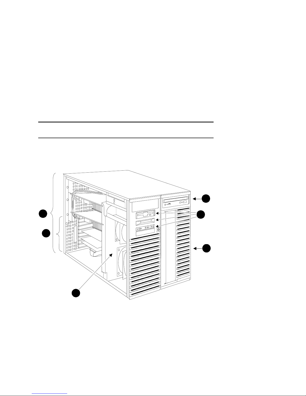
1.1 System Enclosure
The system has up to two CPU modules and up to 4 Gby tes of memory. A single
fast wide UltraSCSI Stora geW orks she lf prov i des up to 128 Gbyte s of storage.
Figure 1-1 System Enclosure
4
1
2
5
PKW-1402-98
3
6
1-2 AlphaServer DS20 Service Manual
Page 13
The numbered callouts in Figure 1-1 refer to the system components.
➊
System card cage, which holds the system board and the CPU, memory, and
system I/O.
➋ PCI/ISA section of the system card cage.
➌ Operator contro l p anel assemb ly, which in cludes th e control p anel, the LC D
display, and the floppy drive.
➍ CD-ROM drive.
➎
Cooling section containing two fans and the server feature module.
➏ StorageWorks shelf.
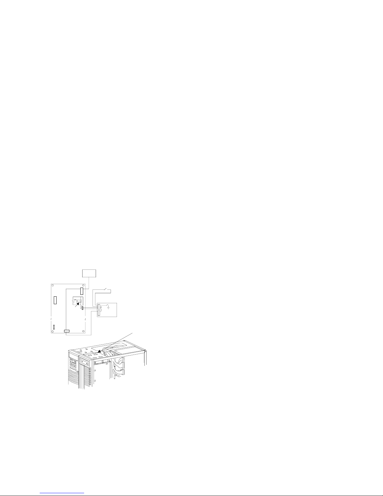
Cover Interlock
The system has a single cover interlock switch tripped by the top cover.
Figure 1-2 Cover Interlock Circuit
Power
Server Feature Module
Switch
pack
Supply
Cover
Interlock
Push button
ON/OFF
OCP
DC_ENABLE_L
OCP
Connector
PK1405-99
NOTE: The cover interlock must be engaged to enable power-up.
To overr ide the cover inter lock, use a s u itable object to close the inter lock cir cuit.
Disk damage will result if the system is run with the top cover off.
Cover
Interlock
Switch
System Overview 1-3
Page 14
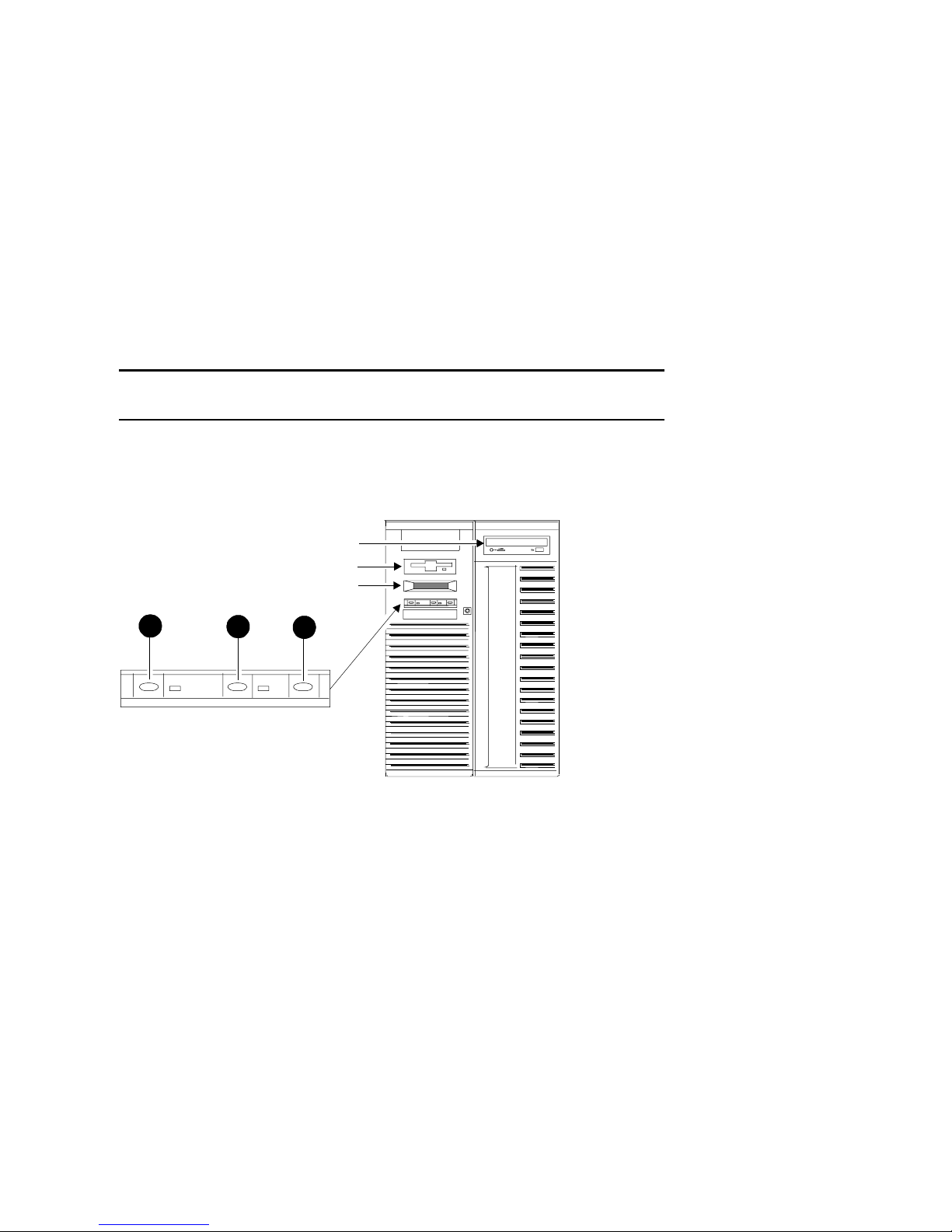
1.2 Operator Control Panel and Drives
The control panel includes the On/Off, Halt, and Reset buttons and an LCD
display.
Figure 1-3 Control Panel Assembly
CD-ROM
Floppy
OCP Display
1
OCP display. The OCP display is a 16-character LCD that indicates status during
power-up and self-test. While the operating system is running, the LCD displays the
system type. Its controller is on the XBUS.
CD-ROM. The CD-ROM drive is used to load software, firmware, and updates. Its
controller i s on P CI1 on th e P C I backplane on the system b oa rd.
Floppy disk. The floppy drive is used to load software and firmware updates. The
floppy c ontrol ler is on the XBUS on the PCI backplane on the system b oard.
2
3
PKW-0501-97
1-4 AlphaServer DS20 Service Manual
Page 15

➊ On/Off button. Powers the system on or off. When the LED to the right of the
button is lit, the power is on. The On/Off button is connected to the power
supplies through the system interlock and the RCM logic.
➋ Rese t but ton. Initializes the system.
➌ Halt button. When the Halt button is pressed, different results are manifest
depending upon the state of the machine.
The major function of the Halt button is to stop whatever the machine is doing
and return the system to the SRM console.
To get to the SRM console, for sy stems r u nni ng OpenVMS o r Compaq Tr u64
UNIX, press the Halt button.
To get to the SRM console, for systems running Windows NT, press the Halt
button and then press the Reset button. (Pressing the Halt button when the
system is running Windows NT causes a “halt assertion” flag to be set in the
firmware. When Reset is pressed, the console reads the “halt assertion” flag and
ignores environment variables that would cause the system to boot.)
The function of the Halt button is complex; it depends upon the state of the
machine when the button is pressed. See Section B.1 for a full discussion of the
Halt button.
System Overview 1-5
Page 16

1.3 System Consoles
There are two console progra ms: the SRM consol e and the AlphaBIOS console.
SRM Console Prompt
On systems running the Compaq Tru64 UNIX or OpenVMS operating system, the
following console prompt is displayed after system startup messages are displayed, or
whenever the SRM console is invoked:
P00>>>
NOTE: The console prompt displays only after the entir e power-u p s equenc e is
complete. This can take up to several minutes if the memory is very large.
AlphaBIOS Boot Menu
On systems running the Windows NT operating system, the Boot menu is displayed
when the AlphaBIOS console is invoked:
1-6 AlphaServer DS20 Service Manual
Page 17

SRM Console
The SRM console is a command-line interface used to boot the Compaq Tru64 UNIX
and OpenVMS operating systems. It also provides support for examining and
modifying the system state and configuring and testing the system. The SRM console
can be run from a serial terminal or a graphics monitor.
AlphaBIOS Console
The AlphaBIOS console is a menu-based interface that supports the Microsoft
Windows NT operating system. AlphaBIOS is used to set up operating system
selections, boot Windows NT, and display information about the system configuration.
The ISA Configuration Utility and the RAID Standalone Configuration Utility are run
from the AlphaBIOS console. AlphaBIOS runs on either a serial terminal or graphics
terminal. Windows NT requires a graphics monitor.
Environment Variables
Environment variables are software parameters that define, among other things, the
system configuration. They are used to pass information to different pieces of
software running in the system at various times . The os_type environment variable,
which can be set to VMS, UNIX, or NT, determines which of the two consoles is used.
The SRM console is always brought into memory, but AlphaBIOS is loaded if os_type
is set to NT and the Halt LED is not lit .
Refer to Appendix A of this guide for a list of the environment variables used to
configure a system.
Refer to your system User’s Guide for information on setting environment variables.
Most environment variables are stored in the NVRAM area of the flash ROM on the
system board. It is recommended that you keep a record of the environment variables
for each system that you service. Some environment variable settings are lost when a
module is swapped and must be restored after the new module is installed. Refer to
Appendix A for a convenient worksheet for recording environment variable settings.
System Overview 1-7
Page 18

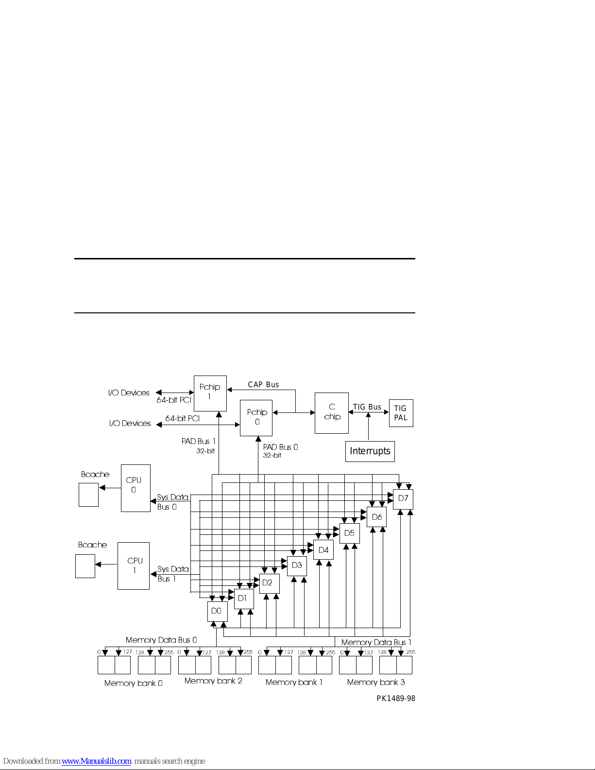
1.4 System Architecture
1 or 2
PKW1400-98
An Alpha microprocessor chi p is use d in this system. The CPU, memo ry, and the
I/O modules are physically connected to the system board and logically connected
through a switch-based interconnect implemented in a cross-bar switch chipset.
Figure 1-4 Block Diagram
Command, Address, and Control lines for each Memory Array
C chip
Control lines for D chips
Probe/
Addr.
CMD/
Addr.
CPU 0
Probe/
Addr.
CMD/
Addr.
CPU 1
(optional)
B cache
CPU
Data
Bus
CAPbus
P chip
P chip
PAD
Bus
64 bit PCI
8 D chips
64 bit PCI
Up to 2
Memory
Banks
Memory
Data
Bus
Memory
Banks
B cache
1-8 AlphaServer DS20 Service Manual
Page 19

The AlphaServer DS20 is a switch-based interconnect system; it uses a cross-bar
switch chipset that allows data to move directly from place to place in the system. The
CPU, memory, and I/O devices physically connect to the system board and each has
one or two logical connections to the switch. The arrows on the block diagram shown
in Figure 1-4 indicate the flow of data, command/address, and control signals.
On the system board is:
• A system switch consisting of a control chip (C-chip) and 8 data chips (D-chips)
• Three buses to the D-chips: the memory data bus, the CPU data bus, and the
P-chip address and data bu s (PAD bus)
• One bus from the C-chip to the P-chips (CAP bus)
• Two 60 command/address and control connections between each CPU and the
C-chip: the command/a d dress li ne f rom the CPUs to the C-chi p and the probe
address lines from the C-chip to the CPUs
• A TIG bus connected to the C-chip
• Control lines from the C-chip to the D-chips
• Control, timing, and address lines from the C-chip to each memory array
• Two 64-bit PCI buses with three PCI option slots each
• One ISA bus bridged on PCI0 and two SCSI ports (unused at FRS) also on PCI0
(If an ISA option is used, PCI 1 slot 9 cannot be used for a PCI option.)
• One ISA to XBUS bridge to the built-in XBUS options
A fully configu red pe desta l syst em can have two CPUs, sixte en DIMMs, a total of six
I/O options, and seven 18 Gbyte UltraSCSI disks. Maximum memory is 4 Gbytes.
The I/O options can be all PCI options or five PCI options and a single ISA option.
Other major lines in the system are used for command, addresses, and control.
For information on CPUs, see Sectio n 1. 5.
For information on memory, see Sections 1.6 and 1.7.
There are two 64-bit PCI buses connected to the cross-bar switch chipset by two PAD
buses and a single CAP bus. Each bus has three PCI slots for I/O devices. PCI bus 0
has an ISA bridge and a SCSI adapter with two ports (not used) embedded on the bus.
A single ISA slot is available on PCI bus 0 that, when used, eliminates the use of one
PCI slot on PCI bus 1.
Logic and sensors on the system feature module monitor power status and the system
environment (temperature and fan speeds).
System Overview 1-9
Page 20

1.5 CPU Types
There is a single CPU variant.
Figure 1-5 CPU Module Placement
1
3
1
DIMM Slo ts
3
0
2
0
2
D
Chip
D
Chip
C
Chip
D
ChipDChip
CPU 0
DIMM Slots
PCI 0 Slot 7
PCI 0 Slot 8
PCI 0 Slot 9
PCI 1 Slot 7
PCI 1 Slot 8
PCI 1 Slot 9
ISA S lo t
D
D
Chip
Chip
2
0
2
0
3
1
3
1
D
ChipDChip
P
ChipPChip
CPU 1
PKW1401A-98
1-10 AlphaServer DS20 Service Manual
Page 21

Alpha Chip Composition
The Alpha 21264 chip uses 0.35 micron chip technology, has a transistor count of 15.2
million, consumes 50 watts of power, and is air cooled (a fan is on the chip). The
default cache system is write-back.
Chip Description
Unit Description
Instruction 64-Kbyte I-cache
Execution 4-way execution; four integer units, two of which can perform
memory address calculations for load and store instructions;
dedicated units for floating-point add, multiply, divide, and
square root operations.
Memory Merge logic, 64-Kbyte write-through first-level data cache,
bus interface unit that consists of two ports, one a 16-byte Bcache port and the other an 8-byte system port.
CPU Variants
Module Variant Clock Frequency Onboard Cache
KN310-Ax 500 MHz 4 Mbytes
CPU Configuration Rules
• The first CPU must be in CPU slot 0.
• Both CPUs must have the same Alpha chi p clo c k spee d selected.
Module LEDs
Description (read LEDs from right to left on the
LED Name
module)
2V_PWRGOOD_LED Normally on. Indicates the presence of 2.XV.
SROM_CLK_LED Normally off. Toggles on and off rapidly during the
SROM load phase.
DC_OK_LED Normally on. Indicates the presence of DC_OK.
CPU_SELF_TEST_LED Normally on. Indicates the status of self-test. If the LED
is off, there was an error or timeout after the SROM load.
System Overview 1-11
Page 22

1.6 Memory
Memory consists of up to four memory options, each consisting of four DIMMs.
There are four option variants: 128 Mbytes, 256 Mbytes, 512 Mbytes, and 1
Gbyte.
Figure 1-6 Memory Placement
1
3
1
DIMM Slo ts
3
0
2
0
2
D
Chip
D
Chip
C
Chip
D
ChipDChip
CPU 0
DIMM Slots
PCI 0 Slot 7
PCI 0 Slot 8
PCI 0 Slot 9
PCI 1 Slot 7
PCI 1 Slot 8
PCI 1 Slot 9
ISA S lo t
D
Chip
2
0
2
0
3
1
3
1
D
Chip
D
ChipDChip
P
ChipPChip
CPU 1
PKW1401B-98
1-12 AlphaServer DS20 Service Manual
Page 23

Memory Variants
Memory is organized on two 256 plus ECC bit buses. Each bus can hold up to two
memory banks (a memory option) made up of four DIMM modules. Memory can be
configured from a minimum of 128 Mbytes (1 MS340-BA) to 4 Gbytes (4 MS340EA). All memory is synchronous.
DRAM
Number/
Option Size Module Type
option Size
MS340-BA 128 MB 54-25066-BA Synch. 36 4 x 32MB
MS340-CA 256 MB 54-25053-BA Synch. 36 4 x 64MB
MS340-DA 512 MB 54-25941-KA Synch. 36 4 x 128MB
MS340-EA 1 GB 54-25941-BA Synch. 36 4 x 256MB
Memory Operation
Two 256-bit memory buses transfer data between the cross-bar chipset switch and
main memory. Each DIMM bank, made up of four DIMM modules, provides the data,
or 256 bits p lus 32 ECC b its, of the 32 by tes transferred. Two modules in the b an k
provide the odd bytes of data, and the other two modules provide the even bytes of
data.
Memory Configuration Rules
In a system, memories of different sizes are permitted, but:
• A memory option consists of four DIMMs all of which must be the same size.
• Convention places the largest memory option in slots marked 0 on the system
board. See Figure 1-6.
• Memory options must be installed in slots designated for each bank. The first
bank goes into slots marked 0, the second bank into slots marked 1, and so on.
System Overview 1-13
Page 24

1.7 Memory Addressing and Data Location
0
0
0
0
PK1488-98
Memory addressing is contiguous beginning with memory bank 0. The first
address of each bank is one above the ending address of the previous bank.
Data is located in DIMMs as described by Figure 1-7.
Figure 1-7 Contents of DIMMs
D
Chip
D
Chip
DIMM Slots
D
Chip
D
Chip
DIMM Contains
Bank 1 even b yt es 0, 2, 4, 6, 8, 10, 12, 14
Bank 3 even bytes 0, 2, 4, 6, 8, 10, 12, 14
Bank 1 even b yt es 16, 18, 20, 22, 24, 26, 28, 3
Bank 3 even b yt es 16, 18, 20, 22, 24, 26, 28, 3
Bank 0 even bytes 0, 2, 4, 6, 8, 10, 12, 14
Bank 2 even bytes 0, 2, 4, 6, 8, 10, 12, 14
Bank 0 even b yt es 16, 18, 20, 22, 24, 26, 28, 3
Bank 2 even b yt es 16, 18, 20, 22, 24, 26, 28, 3
C
Chip
D
Chip
D
Chip
Bank 2 odd bytes 17, 19, 21, 23, 25, 27, 29, 31
Bank 0 odd bytes 17, 19, 21, 23, 25, 27, 29, 31
Bank 2 odd bytes 1, 3, 5, 7, 9, 11, 13, 15
Bank 0 odd bytes 1, 3, 5, 7, 9, 11, 13, 15
Bank 3 odd bytes 17, 19, 21, 23, 25, 27, 29, 31
Bank 1 odd bytes 17, 19, 21, 23, 25, 27, 29, 31
Bank 3 odd bytes 1, 3, 5, 7, 9, 11, 13, 15
Bank 1 odd bytes 1, 3, 5, 7, 9, 11, 13, 15
D
Chip
D
Chip
DIMM Slots
1-14 AlphaServer DS20 Service Manual
Page 25

Memory Addressing
p
Sy
The first address of each bank is one above the ending address of the previous bank.
Examp le 1 –1 and Figure 1-8 show the starting address of each memory bank using
either the SRM console or AlphaBIOS.
Example 1–1 Show Memory
P00>>> show memory
Array # Size Base Addr
------- ---------- -------- 0 128 MB 000000000
1 128 MB 008000000
2 128 MB 010000000
3 128 MB 018000000
Total Ba d Pa ge s = 0
Total Good Memory = 512 MBytes
P00>>>
Figure 1-8 Memory Configuration
Display System Configuration F1= Hel
Systemboard Configuration
Hard Disk Configuration
PCI Configuration
SCSI Configuration
ISA Configuration
Memory Configuration
Integrated Peripherals
æ
Bank 0: 128 MB (32 MB per DIMM)-- Starting Address = 0x000 00000
Bank 1: 128 MB (32 MB per DIMM)-- Starting Address = 0x800 00000
Bank 2: 128 MB (32 MB per DIMM)-- Starting Address = 0x100 00000
Bank 3: 128 MB (32 MB per DIMM)-- Starting Address = 0x180 00000
ESC =Exit
DIMM Contents
Figure 1-7 shows the data contents of each DIMM in memory. Odd data bytes are in
DIMMs below the cross-bar swi tch chip set , a nd the even data byte s are in the DIMMs
above the cross-bar switch chipset.
stem Memory Configuration
System Overview 1-15
Page 26

1.8 System Board
r
r
The system board contains five major logic sections performing five major
system functio ns.
Figure 1-9 System Board
Even bytes
of all memory
banks
I/O
Connector s
Odd bytes
of all memory
banks
PCI 0 Slot 7
PCI 0 Slot 8
PCI 0 Slot 9
PCI 1 Slot 7
PCI 1 Slot 8
PCI 1 Slot 9
ISA Slot
1
3
1
3
0
2
0
2
D
Chip
Chip
2
0
2
0
3
1
3
1
D
Chip
D
D
Chip
C
Chip
D
ChipDChip
D
ChipDChip
P
ChipPChip
TIG
Pal
3 V Power
& Misc 3V
CPU 0
CPU 1
5 V Power
Speaker
Connectors
SCSI
CTRL
ISA
Bridge
Junk I/O
SCSI
Battery
Flash
ROM
Connector
RCM
Connector
Floppy
Connect o
IDE
Connect o
PK1491-98
1-16 AlphaServer DS20 Service Manual
Page 27

Three major sections on the system board are:
• The cross-bar switch chipset and the system components attached to it (CPU(s),
memory, PCI chips, and the TIG bus)
• The power connections and voltage regulator
• The I/O subsystem
System Overview 1-17
Page 28
1.8.1 Cross-Bar Switch and System Components
8
The cross-bar switch chipset consists of a single control chip, the C-chip, and
eight data chips, the D-chips. Into and out of the D-chips are two system buses to
CPUs, two PAD buses to PCI chips, and two memory data buses that connect to
up to four memory banks.
Figure 1-10 Cross-Bar Switch Data Block Diagram
%FDFKH
%FDFKH
,2'HYLFHV
,2'HYLFHV
&38
&38
0HPRU\'DWD%XV
ELW3&,
ELW3&,
3$'%XV
6\V'DWD
%XV
6\V'DWD
%XV
3FKLS
ELW
CAP Bus
3FKLS
3$'%XV
ELW
TIG Bus
FKLS
Interrupts
TIG
PAL
&
'
'
'
'
'
'
'
'
0HPRU\
'DWD%XV
0HPRU\EDQN
0HPRU\EDQN
1-18 AlphaServer DS20 Service Manual
0HPRU\
EDQN
0HPRU\
EDQN
PK1489-9
Page 29

Each type of bus in the system is unique:
• The two memory data buses operate in 256-bit mode passing two hex words (32
bytes) of data between memory and the D-chips per cycle. The bus operates at
83.3 MHz.
• The two CPU data buses operate in “64-bit mode” passing a quadword (8 bytes)
of data between CPU and the D-chips per cycle. Though the CPU data bus is
narrower than the memory data bus, it operates at four times the speed of the
memory data bus at 333 MHz.
• The single CAP bus is a 24-bit wide bidirectional bus that carries commands and
addresses and is also used for transmitting data to and from the C-chip CSRs and
the TIG bus.
• The two PAD buses operate in 32-bit mode passing 8 nibbles per cycle. Two
cycles are required to pass 8 bytes of data. The PAD bus runs at 83.3 MHz.
• The TIG bus handles flash ROM data (system diagnostics and console programs)
and system interrupts.
The cross-bar switch is controlled by the C-chip which synchronizes, along with the
clock, the D-c hips, th e CPUs, me m ory, and the P- chi p s. Figure 1- 10 sho ws the major
data paths through the system.
The C-chip contains:
• Buffers for requests for the P-chips (shared), and each CPU
• Request queues for each memory bank
• A CPU interface for probe and fill requests and issues
• A P-chip interfac e co ntroller and bridg e b etween PCI comman ds and addresses
and CPU PIO commands and addresses
• D-chip contr olle r s, o ne for the PAD bus and one fo r ever yth i ng el se
The D-chip contains:
• Queues to and from t he P-c hip , to an d from th e CPUs, and to and from memory
• Control from the C-chip
The P-chip contains:
• Upstream (away from the PCI) and downstream (toward the PCI) data queues
• Upstream and downstream address queues
• An upstream address state machin e fo r DMA and peer-to-peer reads and writes
• A scatter/gather table for direct mapped and scatter/gather DMA memory access
System Overview 1-19
Page 30

1.8.2 I/O Subsystem
s
The I/O subsystem consists of two 64-bit PCI buses. One has an embedded ISA
bridge, three PCI option slots, and a single ISA sl ot; the other bus has three PCI
option slots.
Figure 1-11 PCI Block Diagram
Crossbar
Switch
8 D Chips
P Chip
PCI 1
I/O ASIC
CAP Bus (24 bits)
P Chip
PCI 0
C Chip
PAD Bus (32 bits)
1 ISA
Slot
Cypress Chip
3&,%XV
PCI-0
3 64-bi t slots
(ISA Bridge,
IDE, KBRD,
MSE, USB)
ADAPTEC
Ultra SCSI
Controller
(2 ports)
1-20 AlphaServer DS20 Service Manual
COM1
COM2
Parallel
Port
Floppy
PCI- 1 B u
PCI-1
3 64-bi t slots
PK1494- 9 8
Page 31

Table 1-1 PCI Slot Numbering
Slot PCI0 PCI1 ISA Shared
5 PCI to ISA bridge ISA device logically
6 Adaptec SCSI
7 PCI slot PCI slot
8 PCI slot PCI slot
9 PCI slot PCI slot ISA device physically
The logic for two PCI buses is on the system board.
• PCI0 is a 64-bit bus with three PCI slots, a Cypress chip, and an Adaptec SCSI
controller. The Cypress chip is the PCI to ISA bus bridge and controls the
following: the keyboard, mouse, IDE bus, real-time clock, and the USB bus. (The
IDE bus an d the USB bus ar e not used.) Conne cted to the ISA bus is an Adapte c
UltraSCSI controller with two ports (also not used).
• PCI1 is a 64-bit bus with three PCI slots.
The cable connector to the floppy is on the system board. Connectors for the mouse,
keyboard, and COM2 are on the bulkhead and are connected directly to the Cypress
chip. The connector for COM1 is also on the bulkhead, but its path is from the
Cypress chip to the RCM connector out to the server featur e module and back throu gh
the RCM co n nector and then to the b u lkhead. The p ath to the OCP is also carri ed
through the RCM connector to the server feature module and then on to the OCP.
System Overview 1-21
Page 32

1.8.3 System Board Switchpacks
PK1410-99
fsb
coa
cob
mdb
sp0
sp1
sp2
pby
cn7
cn2
cn3
cn4
cn5
cn6
spr
flash_wr
There are two switchpacks on the syste m board. They control the wri ting of t he
flash ROM and the speed of the crossbar switch among other things.
Figure 1-12 Switchpack Location
Off On
1
2
3
4
5
6
7
8
SW2
Off On
D
Chip
D
Chip
P
ChipPChip
CPU 0
CPU 1
System Board
1-22 AlphaServer DS20 Service Manual
SW2
SW3
1
2
3
4
5
6
7
8
SW3
Page 33

Figure 1-12 shows the location of the switchpacks and Table 1-2 and Table 1-3
describe what each switch controls.
Table 1-2 Switchpack 2
Switch Description
1 Fail safe bo ot. O ff (defa ult) = normal boot. On = boot the fail safe bo oter
2 Reserved. Must be off.
3 Reserved. Must be off.
4 Reserved. Must be off.
5
6
7
Switches 5, 6, and 7 create a field that defines the speed at which the cross
bar switch runs. Switches 5 and 6 are on and switch 7 is off.
8 AlphaBIOS Password bypass: Off (default) = Normal operation;
On = Bypass AlphaBIOS password
Table 1-3 Switchpack 3
Switch Description
1 Reserved. Must be off.
2 Reserved. Must be off.
3 Reserved. Must be off.
4 Reserved. Must be on.
5 Reserved. Must be off.
6 Reserved. Must be off.
7 Reserved. Must be off.
8 Flash write protect: Off (default) = Write enable the flash ROM
On = Write d isable the fl ash ROM
System Overview 1-23
Page 34

1.9 Server Feature Module
K
The server feature module provides remote control operation of the system. A
four-switch switchpack enables or disables remote control features.
Figure 1-13 Server Feature Module
Power
Connector
RCM
Connector
5 Vaux
Power OK
System Fan
Connectors
Switchpack
Interlock
Connector
Sys Fan OK
CPU Fan O
Temp OK
OCP
Connector
1-24 AlphaServer DS20 Service Manual
PK1492-98
Page 35

The system allows both local and remote control. The remote control firmware and a
set of switches that enable or disable remote control features reside on the server
feature module.
Table 1-4 Remote Control Switch Functions
Switch Condition Function
1 EN RCM
2 Reserved NA Reserved
On (default)
Off
Allows remote system control
Does not allow remote system control
3 RPD DIS On
Off (default)
4 SET DEF On
Off (default)
Disables remote power down
Enables remote power down
Resets the RCM microprocessor defaults
Allows use of conditions set by the user
The defau lt setting s allow comp lete remote control. The user wo uld have to change th e
switch settings to any other desired control.
See Appendix C for information on controlling the system remotely.
The server feature module connects to COM1 on the bulkhead so that its remote
console functions can be accessed. The RCM uses VAUX power provided by the
system power supplies.
The interlock circuit runs through the server feature module as does the path to the
OCP. See Section 1.1.
System Overview 1-25
Page 36

1.9.1 Power Control Logic
K
The power control logic is on the server feature module.
Figure 1-14 Power Control Logic
Power
Connector
RCM
Connector
5 Vaux
Power OK
Switchpack
Interlock
Connector
Sys Fan OK
CPU Fan O
Temp OK
Connectors
Fa n
OCP
Connector
PK1492-98
1-26 AlphaServer DS20 Service Manual
Page 37

The power control logic performs these functions:
• Monitors system temperature and powers down the system 30 seconds after it
detects that internal temperature of the system is above the value of the
environment variable over_temp. Default = 55
0
C.
• Monitors the system and CPU fans and powers down the system 30 seconds after
it detects a fan failur e .
• Provides some visual indication of faults throu gh LEDs.
• Provides I
2
C interface for fans, power supplies, and temp era tur e signals :
Power supply 0, 1: present
Power supply 0, 1: power OK
CPU fan 0, 1: OK
CPU 0, 1: present
Overtemp: Temp OK
System fan 0, 1: OK
Fan Kit OK
System Overview 1-27
Page 38

1.10 Power Circuit and Cover Interlock
Power is distribute d throughout the system and mechanically can be broken by
the On/Off switch, the cover interlock, or remotely through the RCM.
Figure 1-15 Power Circuit Diagram
Power
Supply
Server Feature Module
Switch
pack
OCP
Connector
Cover
Interlock
Push button
ON/OFF
OCP
DC_ENABLE_L
PK1493-98
1-28 AlphaServer DS20 Service Manual
Page 39

Figure 1-15 shows the distribution of the power enable circuit through the system.
Opens in the circui t, or the RCM s ig nal RCM_DC _EN_L, or a power sup ply dete cted
power fault causes interruption to the DC power applied to the system.
A failure anywhere in the circuit will result in the removal of DC power. A potential
failure is the relay used in the remote control logic to control the RCM_DC_EN_L
signal.
The cover interlock is located under the top cover between the system card cage and
the storage area. To override the interlock, place a suitable object in the interlock
switch that closes it.
System Overview 1-29
Page 40

1.11 Power Supply
Two power supplies provide sy stem power.
Figure 1-16 Back of Power Supply and Location
Power
Supply 1
+5V/Return
+3.4V/Return
Current
share
Power
Supply 0
+5V/Return
+12V/Return
Misc.
Signal
PK1495-98
1-30 AlphaServer DS20 Service Manual
Page 41

Description
A single 675 watt power supply provides power to the system. A second power
supply (optional) provides redundant power.
Power Supply Features
• 88–132 and 176–264 Vrms AC input
• 675 watts output. Output voltages are as follows:
Output Voltage Min. Voltage Max. Voltage Max. Current
+5.0 4.85 5.25 100
+3.3 3.18 3.48 100
+12 11.5 12.6 28
–12 –10.9 –13.2 2
+5 Vaux 4.9 5.4 1.5
• Remote sense on +5.0V and +3.3V
+5.0V is sensed on the system board.
+3.3V is sensed on the system board.
• Current share on +5.0V, +3.3V, and +12V.
• 3% regulation on +3.3V.
• Fault protection (latched). If a fault is detected by the power supply, it will shut
down. The power supply faults detected are:
Fan Failure (overtemp)
Overvoltage
Overcurrent
Power overload
• DC_ENABLE_L input signal starts the DC outputs.
• SHUTDOWN_H input signal shuts the power supply off in case of a system fan,
or CPU fan failure, or an overtemp condition detected by the power control logic.
• POK_H output signal indicates that the power supply is operating properly.
System Overview 1-31
Page 42

1.12 Power Up/Down Sequence
System power can be controlled manually by the On/Off button on the OCP or
remotely through t he RCM. The power-up/do wn sequence flo w is shown belo w.
Figure 1-17 Power Up/Down Sequence Flowchart
Apply AC
Power
Vaux on
Off
On-Off
Button
Assert
SHUTDOWN
30 Second
Delay
On
Disa ble Out puts
Deass ert PO K
On-Off Button
RCM Enable OK
Interlock OK
DC_ENABLE_L
Powe r Supply
Yes
No
Fan/Temp
Assert
Star t s
Any
Faults
Assert
POK
OK
On
No
Yes
Off
On
On-Off Button
DC_ENABLE_L
PK1409-99
Off
1-32 AlphaServer DS20 Service Manual
Page 43

When AC is applied to the system, Vaux (auxiliary voltage) is asserted and is sensed
on the server feature module. If the On-Off Button is On, and RCM OK and Interlock
OK are asserted, the OCP asserts DC_ENAB LE _L star ti ng the powe r supplie s. If
there is a hard fault on power-up, the power supplies shut down immediately;
otherwise, the power system powers up and remains up until the system is shut off or
the server feature module senses a fault. If a power fault is sensed, the signal
SHUTDOWN is asserted af ter a 30 secon d delay. Cycling the On-Off button can
restore the power. If the system powers up and shuts off in approximately 30 seconds,
the server feature module has sensed a fault and a fan (system or CPU) is likely
broken.
System Overview 1-33
Page 44

1.13 TIG Bus
The Timing, Interrupt, a nd General bus (TIG) performs a number of functi ons;
it carries all system interrupts, timing signals and provides the path to the
diagnostic and console flash ROMs.
Figure 1-18 TIG Bus Block Diagram
CPU
Data
D Chips
Bus
CPU s
Flash
ROM
PAD
Bus
CAP
Bus
TIG Bus
C ChipP Chip
Config
Registers
and
switchpack
Interrupt
data lines
IRQs
3.
1-34 AlphaServer DS20 Service Manual
Page 45

Figure 1-18 is a block diagram of the TIG bus implemented through the TIG chip.
Three system functions are carried out on this bus.
Flash ROM
The flash ROM containing the diagnostics, fail-safe loader, and console firmware sits
on the TIG bus. (This is different from the AS 1200 where the flash ROM sat on the
2
C bus.) Still a good deal of logic has to function for the diagnostics to run.
I
Configuration Registers
Registers on the bus include interrupts, module information, and clock information.
Interrupts
System interrupts are passed through the TIG bus to the C-chip. The bus connects
directly to PCI slots and to onboard devices.
System Overview 1-35
Page 46

1.14 Maintenance Bus (I2C Bus)
PK1406-99
P-Chip 0
ISA Bridge
There are two I2C buses (referred to as the “I squared C bus”) in this system.
The internal maintena nce bus is used to monitor syste m conditions scanned by
the power control logic on the server feature module, log error state and track
system configuration information. There is a private I
and the C-chip used to provide memory configuration information to the consoles
and operating syste m s.
Figure 1-19 I2C Bus Block Diagram
Server Feature
Module
NVRAM
C-Chip
2
C bus between memory
CPU 0
System
Board
1
I C Bus
Registers
Thermom/
Thermostat
OCP
Controller
2
PCL
Memory
2
I C Bus
Controller
Banks
Private
2
I C Bus
up to 4
XBUS
System
1-36 AlphaServer DS20 Service Manual
Page 47

Monitor
2
C bus monitors the state of system conditions scanned by the power control
The I
logic. There are two registers that the PC logic writes data to:
• One records the state of the fans and power supplies and is latched when there is a
fault.
2
• The other causes an interrupt on the I
C bus when a CPU or system fan fails, an
overtemperature condition exists, or power supplied to the system changes from
N + 1 to N or from N to N +1.
2
The interrupt received by the I
C bus controller and passed on to P-chip 0 alerts the
system of a power system event that may or may not cause a power shutdown. In the
event of imminent power loss the controller has 30 seconds to read the two registers
and store the information in the NVRAM on the server feature module. The SRM
console command show power reads these reg isters .
Fault Display
2
The OCP display is written through the I
C bus.
Error State
Error state is stored for power, fan, and overtemperature conditions on the I
2
C bus.
Configuration Tracking
Each CPU and each logical section of the system board (the PCI bridge, the PCI
backplane, the power control logic, the remote console manager), and the system
board itself has an EEPROM that contains information about the module that can be
written and read over the I
2
C bus. All EEPROMs contain the following information:
• Module type
• Module serial number
• Hardware revision for the logical block
• Firmware revision
System Overview 1-37
Page 48

1.15 StorageWorks Drives
7
The system support s up to seven StorageW orks dri ves.
Figure 1-20 StorageWorks Drive Location
StorageWorks
Drives Shelf
1-38 AlphaServer DS20 Service Manual
PKW0514-9
Page 49

The StorageWorks drives are to the right of the system cage. Up to seven drives fit
into the shelf. The system supports fast wide UltraSCSI disk drives. The RAID
controller is also supported. With an optional UltraSCSI Bus Splitter Kit, the
StorageWorks shelf can be split into two buses.
System Overview 1-39
Page 50

Page 51

Chapter 2
Troubleshooting
This chapter describes troubleshooting during power-up and booting. It also describes
the console test command and other service related console commands. A Compaq
Analyze example is also provided. The following topics are covered:
• Troubleshooting During Power-Up
• Control Panel Display and Troubleshooting
• Power-Up Display and Troubleshooting
• Running Diagnostics — Test Command
• Testing an Entire System
• Other Useful Console Commands
• Troubleshooting with LEDs
• Compaq Analyze
• Releasing Secure Mode
Troubleshooting 2-1
Page 52

2.1 Troubleshooting During Power-Up
Power or other problems can occ ur before the syste m is up and running.
Power Problem List
The system will halt/power off for the following reasons:
1. A CPU fan failure
2. A system fan failure
3. An overtemperature condition
4. Power supply failure if the redundant power option is not present
5. Circuit beaker(s) tripped
6. AC problem
7. Interloc k sw itch activation or failure
8. Environmental electrical failure or unrecoverable system fault with auto_action ev
= hal t or b oot
9. Cable failure
Indication of failure
• LEDs on the server feature module indicate fan, overtemperature, and power
problem conditions.
• Circuit breaker(s) tripped at the AC service panel.
• There is no obvious indication for failures 7 – 9 from the power system.
Beep Codes
Number Definition
1, 2, 3 beeps The firmware in flash ROM is corrupt.
4 beeps T he header in the ROM is not valid.
6 beeps A checksum error occurred after the ROM image was copied into
memory.
2-2 AlphaServer DS20 Service Manual
Page 53

If the system does not power up
• Are the power cords plugged in?
• Is the power supply functioning? (The power supply will shut down if it detects
any faults. See Section 1.11.)
• Are the cover and side panels closed and the interlock engaged?
If the system comes up and approximately 30 seconds later goes down,
possible failures are:
• CPU fan failure
• System fan failure
• Overtemperature condit io n
If you hear a series of beeps (1, followed by 2, followed by 3)
These beeps indicate that the firmware in flash ROM is corrupt. The machine hangs
and the floppy light goes on.
Action:
1. On a working machine, insert the Alph a Syste m s Firmwa re Update Ve rsion V5.4
(minimum rev.) CD in the CD-ROM drive and copy the file PC264SRM.ROM
found in the DS20 subdirectory onto a floppy renaming the file to
DP264SRM.ROM.
2. Insert the floppy you just made into the floppy drive on the broken system.
3. Using the On/Off button, turn the machine off and then back on. The SRM
console will load from the floppy.
4. Place the Alpha Systems Firmware Update CD in the CD-ROM drive.
5. Run LFU and update the firmware.
Refer to Appendix C for instructions on updating firmware.
If you hear four beeps
The header in the ROM is not valid, and the system will not boot. Replace the system
board.
If you hear six beeps
Six beeps indicate a checksum error occurred after the ROM image was copied into
memory. Either memory is misconfigured or a memory DIMM needs to be reseated.
Troubleshooting 2-3
Page 54

2.2 Control Panel Display and Troubleshooting
The control panel display indicates the likely device when testing fails.
Figure 2-1 Control Panel and LCD Display
AlphaServer DS20
PK1408
• When the On/Off button LED is on, power is applied and the system is running.
When it is off, the system is not running, but power may or may not be present. If
the power supplies are receiving AC power, Vaux is present on the server feature
module regardless of the condition of the On/Off switch.
• When the Halt button LED is lit and the On/Off button LED is on, the system
should be running either the SRM console or Windows NT.
2-4 AlphaServer DS20 Service Manual
Page 55

Table 2-1 Control Panel Display
Content of Display Progress Indicated in Power-Up Flow
Compaq CPU functioning, path to the OCP operating. Hardware
involved – CPU, C-chip, P-chip 0, PCI to ISA bridge,
ISA to XBUS bridge, OCP contro ll e r.
Compaq * B-cache initialized and both B-cach e and memory is
being tested. Additional hardware involved: Backup
cache on the CPU module, D-chips, memory DIMMs.
Compaq Firmware Firmware loading. Additional hardware involved – TIG
bus.
Compaq Error 06
Probe I/O Subsystem SRM console probing the system. Additional hardware
AlphaServer DS20 Either the SRM console or AlphaBIOS are up and
Memory error. No memory was found, or memory is
bad, or misconfigured, or needs re-seating.
involved – P-chip 1, all devices on both PCIs.
running.
Troubleshooting 2-5
Page 56

2.3 Power-Up Display and Troubleshooting
If the power-up display appears, the following hardware is at least partially
functioning: at least one CPU, the C-chip, some D-chips, the P-chips, the TIG
bus, the ISA bridge, and the I
serial terminal (if the console environment variable is set to serial); the last
several lines print to either a serial terminal or a graphics monitor. Power-up
status also is seen on the control panel di spl ay.
Example 2–1 Power-Up Display
512 Meg of system memory ➊
probing hose 1, PCI ➋
bus 0, slot 7 -- pka -- QLogic ISP1040
bus 0, slot 8 -- ewa -- DECchip 21140-AA
probing hose 0, PCI
probing PCI-to-ISA bridge, bus 1
bus 0, slot 5, function 1 -- dqa -- Cypress 82C693 IDE
bus 0, slot 5, function 2 -- dqb -- Cypress 82C693 IDE
bus 0, slot 6, function 0 -- pkb -- Adaptec AIC-7895
bus 0, slot 6, function 1 -- pkc -- Adaptec AIC-7895
bus 0, slot 7 -- vga -- DEC PowerStorm
bus 0, slot 8 -- ewa -- DECchip 21040-AA
Testing the System
Testing the Disks (read only)
Testing the Network
System Temperature is 22 degrees C
2
C bus. The entire power-up display prints to a
➌
Compaq AlphaServer DS20 Console V5.4, Aug 26 1998 16:07:57 ➍
P00>>>
2-6 AlphaServer DS20 Service Manual
Page 57

By the time the power-up display is completed,
1. the CPUs have run their self-te sts,
2. the SROM has completed its preliminary tests and loaded the SRM console from
flash ROM on the TIG bus into memory,
3. the SROM has passed control to the SRM console,
4. the SRM has polled the system , r un its sy stem dia g nost ic s, a nd has sent t he
display characters.
If the system’s operating system is NT, you will not see any of the power-up display
before the line that says “Testing the System.”
➊ Memory size is determined by the C-chip.
➋ The PCI bridges and attendant buses (indicated as IODn by the cons o le) are
probed and the devices are reported. I/O adapters are configured. At a
minimum, the devices are responding to probes by the console program.
➌ The system, disks, and network are tested by the console.
➍ The SRM console banner and prompt are printed. (The SRM prompt is shown in
this manual as P00>>>. It can, however, be P01>>>. The number indicates the
primary processor.) If the auto_action environment variable is set to boot or
restart an d the os_type environment variable is set to unix or openvms, the
Compaq Tru64 UNIX or OpenVMS operating system boots.
If the system is running the Windows NT operating system (the os_type
environment variable is set to nt), the SRM console loads and starts the
AlphaBIOS console.
Refer to Chapters 4 and 5 of the AlphaServer DS20 User’s Guide for
information about the SRM console and AlphaBIOS.
Troubleshooting 2-7
Page 58

2.4 Running Diagnostics — Test Command
The test command runs diagnostics on the entire system, CPU devices, memory
devices, and the PCI I/O subsystem. The test command runs only from the SRM
console. Ctrl/C stops the test . T he console canno t be sec ure.
Example 2–2 Test Command Syntax
P00>>> help test
NAME
test
FUNCTION
Test the system.
SYNOPSIS
test [-lb] [-t <time>]
COMMAND ARGUMENT(S):
P00>>>
P00>>>
P00>>>
SYNOPSIS
test ([-lb] [-t <time>]
The entire system is tested by default.
NOTE: If you are running the Microsoft Windows NT operating system, switch from
AlphaBIOS to the SRM console in order to enter the test command. From th e
AlphaBIOS console, press in the Halt button (the LED will light) and reset the system,
or select Tru64 UNIX (SRM) or OpenVMS (SRM) from the Advanced CMOS Setup
screen and reset the system.
test [-lb] [-t time]
-lb Loop back test enable. Loop back connectors are needed on COM1,
COM2, and the parallel port.
-t time Specifies the run time in seconds. The default for system test is 600
seconds (10 minutes).
2-8 AlphaServer DS20 Service Manual
Page 59

2.5 Testing an Entire System
A test command runs all exercisers for subsystems and devices on the system.
I/O devices tested are suppor ted bo o t devices. The test runs f or 2 minute s.
Example 2–3 Sample Test Command
P00>>> test
System test, runtime 120 seconds
Type ^C if you wish to abort testing once it has started
Default zone extended at the expense of memzone.
Use INIT before booting
Testing Ethernet device(s)
Testing VGA
Testing Memory
Testing SCSI disks (read-only)
Testing other SCSI devices (read-only)..
Testing floppy drive (dva0, read-only)
No diskette present, skipping floppy test
ID Program Device Pass Hard/Soft Bytes Wrtn Bytes Rd
-------- ------------ ---------- ----- -------- ---------- ---------00001c12 memtest memory 1 0 0 352321536 352321536
00001c17 memtest memory 1 0 0 352321536 352321536
00001c35 memtest memory 1 0 0 352321536 352321536
00001c80 exer_kid dkb100.1.0.9 0 0 0 0 4915200
00001c83 exer_kid dkb200.2.0.9 0 0 0 0 4898816
00001c85 exer_kid dkb300.3.0.9 0 0 0 0 4898816
00001cc7 exer_kid dke0.0.0.200 0 0 0 0 6144000
00001cc8 exer_kid dke200.2.0.2 0 0 0 0 6144000
00001cc9 exer_kid dke400.4.0.2 0 0 0 0 6127616
00001cf7 exer_kid dkf100.1.0.2 0 0 0 0 8830976
00001cfa exer_kid dkf300.3.0.2 0 0 0 0 8814592
ID Program Device Pass Hard/Soft Bytes Wrtn Bytes Rd
-------- ------------ ---------- ---- ---------- ---------- --------00001c12 memtest memory 1 0 0 713031680 713031680
00001c17 memtest memory 1 0 0 721420288 721420288
00001c35 memtest memory 1 0 0 713031680 713031680
00001c80 exer_kid dkb100.1.0.9 0 0 0 0 12730368
00001c83 exer_kid dkb200.2.0.9 0 0 0 0 12713984
00001c85 exer_kid dkb300.3.0.9 0 0 0 0 12713984
00001cc7 exer_kid dke0.0.0.200 0 0 0 0 8749056
00001cc8 exer_kid dke200.2.0.2 0 0 0 0 8749056
00001cc9 exer_kid dke400.4.0.2 0 0 0 0 8749056
00001cf7 exer_kid dkf100.1.0.2 0 0 0 0 13533184
00001cfa exer_kid dkf300.3.0.2 0 0 0 0 13516800
Continued on next page
Troubleshooting 2-9
Page 60

ID Program Device Pass Hard/Soft Bytes Wrtn Bytes Rd
-------- ------------ ---------- ----- -------- ---------- ---------00001c12 memtest memory 2 0 0 1082130432 1082130432
00001c17 memtest memory 2 0 0 1082130432 1082130432
00001c35 memtest memory 2 0 0 1073741824 1073741824
00001c80 exer_kid dkb100.1.0.9 0 0 0 0 20086784
00001c83 exer_kid dkb200.2.0.9 0 0 0 0 20086784
00001c85 exer_kid dkb300.3.0.9 0 0 0 0 20086784
00001cc7 exer_kid dke0.0.0.200 0 0 0 0 16531456
00001cc8 exer_kid dke200.2.0.2 0 0 0 0 16515072
00001cc9 exer_kid dke400.4.0.2 0 0 0 0 16515072
00001cf7 exer_kid dkf100.1.0.2 0 0 0 0 23511040
00001cfa exer_kid dkf300.3.0.2 0 0 0 0 23494656
ID Program Device Pass Hard/Soft Bytes Wrtn Bytes Rd
-------- ------------ ---------- ----- -------- ---------- ---------00001c12 memtest memory 2 0 0 1442840576 1442840576
00001c17 memtest memory 2 0 0 1442840576 1442840576
00001c35 memtest memory 2 0 0 1442840576 1442840576
00001c80 exer_kid dkb100.1.0.9 0 0 0 0 28852224
00001c83 exer_kid dkb200.2.0.9 0 0 0 0 28852224
00001c85 exer_kid dkb300.3.0.9 0 0 0 0 28852224
00001cc7 exer_kid dke0.0.0.200 0 0 0 0 19513344
00001cc8 exer_kid dke200.2.0.2 0 0 0 0 19513344
00001cc9 exer_kid dke400.4.0.2 0 0 0 0 19513344
00001cf7 exer_kid dkf100.1.0.2 0 0 0 0 29917184
00001cfa exer_kid dkf300.3.0.2 0 0 0 0 29900800
ID Program Device Pass Hard/Soft Bytes Wrtn Bytes Rd
-------- ------------ ---------- ----- -------- ---------- ---------00001c12 memtest memory 2 0 0 1803550720 1803550720
00001c17 memtest memory 2 0 0 1811939328 1811939328
00001c35 memtest memory 2 0 0 1803550720 1803550720
00001c80 exer_kid dkb100.1.0.9 0 0 0 0 36241408
00001c83 exer_kid dkb200.2.0.9 0 0 0 0 36241408
00001c85 exer_kid dkb300.3.0.9 0 0 0 0 36241408
00001cc7 exer_kid dke0.0.0.200 0 0 0 0 26968064
00001cc8 exer_kid dke200.2.0.2 0 0 0 0 26968064
00001cc9 exer_kid dke400.4.0.2 0 0 0 0 26968064
00001cf7 exer_kid dkf100.1.0.2 0 0 0 0 38158336
00001cfa exer_kid dkf300.3.0.2 0 0 0 0 38158336
^C
P00>>>
2-10 AlphaServer DS20 Service Manual
Page 61

2.6 Other Useful Console Commands
Several console comma nds can be use d to diagnose the syste m.
The show power command identifies power, temperature, and fan faults.
Example 2–4 Show Power
P00>>> show power
Status
Power Supply 0 good
Power Supply 1/Fan Tray good
System Fans good
CPU Fans good
Temperature good
Current ambient temperature is 27 degrees C
System shutdown temperature is set to 55 degrees C
1 Environmental events are logged in nvram
Do you want to view the events? (Y/<N>) y
Total Environmental Events: 1 (1 logged)
1 NOV 11 18:00 System Fan 0 Failure, Power Supply 0,1 Failure
Do you want to clear all events from nvram? (Y/<N>) n
P00>>>
The show memory command shows memory DIMMs and their starting addresses.
Example 2–5 Show Memory
P00>>> show memory
Array # Size Base Addr
------- ---------- -------- 0 512 MB 000000000
1 512 MB 020000000
2 256 MB 040000000
3 128 MB 050000000
Total Bad Pages = 0
Total Good Memory = 1408 MBytes
P00>>>
Troubleshooting 2-11
Page 62

2.7 Troubleshooting with LEDs
K
During power-up, reset, initialization, or testing, diagnostics are run on CPUs,
memories, P-chi ps, and the PCI backplane and its embedded options. Although
system LEDs are not visible when the side pa nel s are on, they ca n be viewed when
the card cage side of the system is exposed and the top cover is on. There are
LEDs on the CPU and server feature modules.
Figure 2-2 CPU and Server Feature Module LEDs
CPU Self-test
CPU DC OK
SROM Clk
2V OK
5V OK
CPU
Module
Server
Feature
Module
5 Vaux
Power OK
2-12 AlphaServer DS20 Service Manual
Sys Fan OK
CPU Fan O
Temp OK
PK1407-99
Page 63

To see LEDs, the card cage side of the system must be exposed; the system top should
be on, and the system must be on.
CPU LEDs
The CPU LEDs are on the under side of the module. Figure 2-2 shows the location of
the LEDs when looking up at the module. Normally all CPU LEDs are on except the
SROM Clock LED.
Replace the CPU if the 5V OK LED is on and any of the following LEDs are off: CPU
DC OK, or 2V OK.
If the 5V OK LED is off, power is not getting to the CPU. The problem could be the
power harness, the power translation board, the power supply, or the CPU.
If the CPU self-test LED is off, the built-in self-test on the CPU chip did not complete
for some reason.
Server Feature Module LEDs
All the LEDs on this module are normally on.
If the 5 Vaux Power OK LED is off, power is not getting to the module and the
problem could be the power harness, the power translation board, the power supply, or
the server feature module.
If the Sys Fan OK LED is off, a system fan is broken. Use the show power command
to determine which.
If the CPU Fan OK LED is off, a CPU fan is broken. Use the show power command
to determine which.
If the Temp OK LED is off, the temperature in the cabinet is above the temperature
thresho ld. Several th ings can cause this con dition: b locked airf low, temp er ature in the
room where the system is located is too high, the system card cage is open and air is
not channeled properly over the system. Fix any of these conditions, if possible. The
overtemperature threshold is programmable and is controlled by the environment
variable over_temp. Its default is 55 degrees C. After the system has cooled down
and can be powered up, you can change the threshold. If you do this and the
temperature inside the system gets too hot, it is likely that system errors will occur and
the system may crash. If the system gets too hot, hardware can be damaged.
Troubleshooting 2-13
Page 64

2.8 Compaq Analyze
Compaq Analyze is the error analysis tool used to analyze errors. An example of
its output is shown here. For information on installing, running, and learning
about Compaq Analyze, go t o http: // www.e v nr ud.c x o. dec .c o m/desta/kits. htm.
2.8.1 Compaq Analyze Graphics Interface (GUI)
Compaq Analyze automatically runs on each of the supported operating systems
on the DS20 system.
Figure 2-3 Compaq Analyze Graphics Interface
2-14 AlphaServer DS20 Service Manual
PK1411-99
Page 65

Figure 2-3 shows an example of what you can expect to see on a system’s console,
assuming it is a graphics terminal and Compaq Analyze is installed and running in the
backround. When an error is detected, it is reported to the console with a series of
problem found statements. In this case, “an uncorrectable system fan 0 error
detected,” was logged a couple of times in the event log with a time stamp of Friday
March 12, 1999.
To get a full analysis of the error, double click on the Problem Found: hot spot on the
active screen and a full report of the error is displayed.
Troubleshooting 2-15
Page 66

2.8.2 Description of the Error
After “double clicking” the Problem Found: hot spot on the Compaq Analyze
screen a full description of the error is displayed and a FRU and its location is
called out. Example 2–6 shows a Compaq Analyze error report.
Example 2–6 Compaq Analyze Error Report
Problem Found: An uncorrect able sy stem fan 0 error det ected.
Managed Entity:
System Entity: enugu Error Environment:
Record Number :
Event ID_Count:2Ev ent ID_P refi x:15 008
Event Time:
Time of Error : Thu, 11 Mar 1999 12:43:58 –0500
Brief Description:
An uncorrectable system fan 0 error detected.
Callout ID:
0020050000072E05
Severity:
2
Reporting Node:
enugu
Full Description:
An uncorrectable system fan 0 error has been diagnosed. This System
error requires replacement service to be administered to Fan 0 Field
Replaceable Unit (FRU). This FRU is physically located in the
compartment to the right of the system card cage and is System Fan 0
– Upper Fan.
FRU List:
Probability: High
Manufacturer: Comp aq
Device Type: Power, Cooling, and Temperature
Physical Location: Slot System Fan 0 -FRU Part Number: System fan 0 pn from config tree
FRU Serial Number: Fru SN from config tree
FRU Firmware Rev: NA
2-16 AlphaServer DS20 Service Manual
Page 67

Evidence:
Entry Errlog: SMM_1838 SysType _34 OS_T ype_ 1 Entry_ Type _682
Entry_Type_Ana Mchk_Error_Cod
Event_Header_Common_Fields_V2_0
Event_Leader: xFFF FFFF E
Header_Length: 176
Event_Length: 312
Header_Rev_Maj or: 2
Header_Rev_Min or: 0
OS_Type: 1 ! 1 = UNIX, 2 = OVMS, 3 = NT
Hardware_Arch: 4
CEH_Vendor_ID: 3564
Hdwr_Sys_Type: 34
Logging_CPU: 0
CPUs_In_Active_Set: 2
Major_Class: 115
Minor_Class: 2
DSR_Msg_Num: 1838 !
CEH_Device: 35
Chip_Type: 8 ! 8 = EV6
CEH_Device_ID_0: x0000FFFF
CEH_Device_ID_1: x00000000
CEH_Device_ID_2: x00000000
Unique_ID_Count: 2
Unique_ID_Pref ix: 1500 8
Num_Strings: 2
Event_Header_UNIX_WNT_Specific_Fields_V2_0
Priority: 3
DID_Fmt: x00
Subid_Errcode: xFFFFFFFF
Subid_Num: 0
TLV_Processing_Support
TLV_Time_as_Local: Thu, 11 Mar 1999 12:43:58 -0500
TLV_Computer_Name: enugu
SMM_Decode_Support
System_Marketing_Model: 1838 !
System_Type: 34
Chip_Type: 8
Member_ID: 6
Chip_Speed: 500
Number_of_CPUs: 1
Entry_Type_Support
Entry_Type: 682 ! Machine Check type 682 (environment error)
Compaq AlphaServer
Compaq AlphaServer
DS20
DS20
Continued on next page
Troubleshooting 2-17
Page 68

Systype34_Env_Regs_V1
Frame_Flags: x00000000
Mchk_Error_Code: x00000206
Frame_Rev: 1
SW_Sum_Flags: x000 0000 0000 0000 0
Cchip_DIR: x0001000000000000
Environ_QW_1: x000 0000 0000 0000 9
Environ_QW_2: x000 0000 0000 0004 F
Environ_QW_3: x000 0000 0000 0000 0
Environ_QW_4: x000 0000 0000 0000 0
Environ_QW_5: x000 0000 0000 0000 0
Environ_QW_6: x000 0000 0000 0000 0
Environ_QW_7: x000 0000 0000 0000 0
Environ_QW_8: x000 0000 0000 0000 0
Environ_QW_9: x000 0000 0000 0000 0
Subpacket_Supp ort
Subpacket_Head er_S uppo rt
Trailer_Frame_ Supp ort
Compaq Analyze Problem Report
2-18 AlphaServer DS20 Service Manual
Page 69

Of particular interest in the error report is the Full Description of the error. If
Compaq Analyze is able to determine what failed on the machine, it gives a full
description of the failing FRU and its location. In this case the upper system fan is
identified as the failing part and its location is given.
Evidence provided depends upon the type of error detected. The types of errors
detected are given in Table 2-2. The evidence section of the Compaq Analyze report
provides information that lead the tool to identify the failing FRU and its location. For
more information, see the Regatta Platform Fault Management Specification.
Table 2-2 Types of Errors
Error Event Description
MCHK 670 Processor Machine checks. These are synchronous errors that
inform precisely what happened at the time the error occurred.
They are detected inside the CPU chip and are fatal errors.
MCHK 660 System machine checks. These are asynchronous errors that are
recorded after the error has occurred. Data on exactly what was
going on in the machine at the time of the error may not be
known. They are fatal errors.
MCHK 630 Processor correctable errors.
MCHK 620 System correctable errors.
MCHK 682 - 685 System environment failures that require repair (power supply
failure, system fan failure, overtemperature condition).
MCHK 687 Redundant power supply failure.
Troubleshooting 2-19
Page 70

2.9 Releasing Secure Mode
The console cannot be secure for most SRM console commands to run. If the
console is not secure, user mode console commands can be entered. See the
system manager if the syste m is secure and you do not know the passwor d.
Example 2–7 Releasing/Reestablishing Secure Mode
P00>>> login
Please enter password: xxxx
P00>>>
[User mode SRM console commands are now available.]
P00>>> set secure
The console command login clears secure.
If the password has been forgotten and the system is in secure mode, enter the login
command:
P00>>> login
please enter password:
At this prompt, press the Halt button and then press the Return key.
The password is now cleared and the console is in user mode. A new password must
be set to put the console into secure mode again.
For a full discussion of securing the console, see your system User’s Guide.
2-20 AlphaServer DS20 Service Manual
Page 71

Chapter 3
Error Registers
This chapter describes the following registers used to hold error information:
• Ibox Status Register - I_STAT
• Memory Management Status Register – MM_STAT
• Dcache Status Register – DC_STAT
• Cbox Read Register
• Miscellaneous Register (MISC)
• Device Interrupt Request Register (DIRn, n=0,1)
• Pchip Error Register (PERROR)
• Failure Register
• Function Register
Error Registers 3-1
Page 72

3.1 Ibox Status Register - I_STAT
3
The Ibox Status Register (I_STAT) is a read/write-1-to-clear register that
contains Ibox status information. The register is read only by PAL code and is
an element in the CPU or System Uncorrectable Machine Check Error Logout
frame.
3031 29 28
TPE
DPE
61
PK1414-99
Table 3-1 Ibox Status Register
Name Bits Type Description
Reserved <63:31> RO Reserved for Compaq.
DPE
<30> W1C
TPE <29> W1C
Icache data parity error
When set, indicates that the Icache
encountered a data parity error on instruction
fetch.
Icache tag parity error
When set, indicates that the Icache
encountered a tag parity error on instruction
fetch.
0
2
Reserved <28:0> RO Reserved for Compaq.
3-2 AlphaServer DS20 Service Manual
Page 73

3.2 Memory Management Status Register –
3
MM_STAT
The Memory Management Status Register (MM_STAT) is a read-only register.
When a Dstream TB miss or fault occurs, information about the error is latched
in MM_STAT. This register is not updated when a LD_VPTE gets a DTB miss
instruction. The register is read only by PALcode and is an element in the CPU
or System Uncorrectable Machine Check Error Logout frame.
61
31
DC_TAG_PERR
OPCODES<5:0>
FOW
FOR
ACV
WR
2
1011 49321
0
PK1415-99
Error Registers 3-3
Page 74

Table 3-2 Memory Management Status Register
Name Bits Type Description
Reserved <63:11> Re served for Compaq.
DC_TAG
_PERR
<10> RO This bit is set when a Dcache tag parity error occurs
during the initial tag probe of a load or store
instruction. The error created a synchronous fau lt
to the D_FAULT PALcode entr y poi nt and is
correctable. The virtual address associated with the
error is available in the VA register.
OPCODE <9:4> RO Opcode of the instruction that caused the error.
HW_LD is displayed as 3 and HW_ST is displayed
as 7.
FOW < 3> RO Set when a fault-on-write error occurs during a
write transaction and PTE[FOW] was set.
FOR <2> RO Set when a fault-on-read error occurs during a read
transaction and PTE[FOR] was set.
ACV <1> RO Set when an access violation occurs during a
transaction. Access violations include a bad virtual
address.
WR < 0> RO Set when an error occurs during a write transaction.
3-4 AlphaServer DS20 Service Manual
Page 75

3.3 Dcache Status Register – DC_STAT
3
1
The Dcache Status Register (DC_STAT) is a read-write register. If a Dcache tag
parity error or data ECC error occurs, information about the error is latched in
this register. The register is read only by PALcode and is an element in the CPU
or System Uncorrectable Machine Check Error Logout frame.
61
31
ECC_ERR_LD
ECC_ERR_ST
TPERR_P1
TPERR_P0
SEO
432
PK1416-99
2
0
Error Registers 3-5
Page 76

Table 3-3 Dcache Status Register
Name Bits Type Description
Reserved < 63:5> Reserved for Compaq.
SEO < 4> W1C Second error occured. When set, indicates that a
second Dcache store ECC error occurred within 6
cycles of the previous Dcache store ECC error.
ECC_ERR
_LD
<3> W1C ECC error on load. When set, indicates that a
single-bit ECC error occurred while processing a
load from the Dcache or any fill.
ECC_ERR
_ST
<2> W1C ECC error on store. When set, indicates that an
ECC error occurred while processing a store.
TPERR_P1 <1> W1C Tag parity error — pipe 1. When set, indicates that
a Dcache tag probe from pipe 1 resulted in a tag
parity error. The error is uncorrectable and results
in a machin e check.
TPERR_P0 <0> W1C Tag parity error — pipe 0. When set, this bit
indicates that a Dcache tag probe from pipe 1
resulted in a tag parity error. The error is
uncorrectable an d r es u lts in a machine che ck.
3-6 AlphaServer DS20 Service Manual
Page 77

3.4 Cbox Read Register
The Cbox Read Register is read 6 bits at a time. Table 3-4 shows the ordering
from LSB to MSB. The register is read only by PALcode and is an element in the
CPU or System Uncorrectable Machine Check Error Logout frame.
Table 3-4 Cbox Read Register
Name Description
C_SYNDROME_1
<7:0>
C_SYNDROME_0
<7:0>
C_STAT<4:0>
Syndrome for the upper QW in the OW of victim that was
scrubbed.
Syndrome for the lower QW in the OW of victim that was
scrubbed.
Bits Error status
00000 Either no error, or error on a speculative load, of a
Bcache victim read due to a Dcache/Bcache miss.
00001 BC_PERR (Bcache tag parity error)
00010 DC_PERR (duplicate tag parity error
00011 DSTREAM_MEM_ERR
00100 DSTREAM_BC_ERR
00101 DSTREAM_DC_ERR
0011X PROBE_BC_ERR
01000 Reserved
01001 Reserved
01010 Reserved
01011 ISTREAM_MEM_ERR
01100 ISTREAM_BC_ERR
01101 Reserved
1XXXX DOUBLE_BIT_ERROR
Error Registers 3-7
Page 78

Table 3-4 Cbox Read Register (Continued)
Name Description
C_STAT<3:0>
C_ADDR
<6:42>
If C_STAT equals xxx_MEM_ERR or xxx_BC_ERR, then
C_STAT contains the status of the block as follows; otherwise, the
value of C_STAT is X.
Bit valus Status of block
7 - 4 Reserved
3 Parity
2 Valid
1 Dirty
0 Shared
Address of the last reported ECC or parity error. If C_STAT value
is DSTREAM_DC_ERR, only bits <6:19> are valid.
3-8 AlphaServer DS20 Service Manual
Page 79

3.5 Miscellaneous Register (MISC)
This register is designed so that only writes of 1 affect it. When a 1 is written to
any bit in the register, the programmer does not need to be concerned with readmodify-write or the status of any other bits in the register. Once NXM is set, the
NXS field is locked. It is unlocked when software clears the NXM field. The
ABW (arbitration won) field is locked if either ABW bit is set, so the first CPU to
write it locks out the other CPU. Writing a 1 to ACL (arbitration clear) clears
both ABW bits and both ABT (arbitration try) bits and unlocks the ABW field.
Address 801 A000 0040
Access RW
63
44 43 40 39
reserved
DEVSUP
REV
31 43
29 28 27 2524 23 20 19 16 15 12 11 8 7 2 1
000
00
NXM
NXS
ACL
ABT
ABW
IPREQ
IPINTR
ITINTR
CPUID
32
0
PK1417-99
Error Registers 3-9
Page 80

Table 3-5 Miscellaneous Register
Initial
Name Bits Type
RES <63:44> MBZ, RAZ 0 Reserved.
DEVSUP <43:40> WO 0
REV <39:32> RO 1 Latest revision of the Cchip:
NXS <31:29> RO 0 NXM source – Device that
NXM <28> R, W1C 0 Nonexistent memory address
RES <27:25> MBZ, RAZ 0 Reserved.
ACL <24> WO 0 Arbitration clear – writing a 1
ABT <23:20> R, W1S 0 Arbitration try – writing a 1 to
State Description
1 = Tsunami
caused the NXM.
Unpredictable if NXM not set.
0 = CPU0, 1 = CPU1.
detected. Sets DRIR<63> and
locks the NXS field until it is
cleared.
to this bit clears the ABT and
ABW fields.
these bits sets them.
ABW <19:16> R, W1S 0 Arbitration won – writing a 1
IPREQ <15:12> WO 0 Inter proc essor int errup t
IPINTR <11:8> R, W1C 0 Interprocessor interrupt
3-10 AlphaServer DS20 Service Manual
to these bits sets them unless
one is already set, in which
case the write is ignored.
request – write a 1 to the bit
corresponding to the CPU you
want to interrupt. Writing a 1
here sets the corresponding bit
in the IPINTR.
pending – one bit per CPU.
Pin irq<3> is asse r ted to the
CPU corresponding to a 1 in
this field.
Page 81

Table 3-5 Miscellaneous Register (Continued)
Initial
Name Bits Type
ITINTR <7:4> R, W1C 0 Interval timer interrupt
RES <3:2> MBZ, RAZ 0 Re served.
State Description
pending – one bit per CPU.
Pin irq<2> is asserted to the
CPU corresponding to a 1 in
this field.
CPUID <1:0> RO -
ID of the CPU performing the
read.
Error Registers 3-11
Page 82

3.6 Device Interrupt Request Register (DIRn, n=0,1)
These registers indi cate which interrupts are pending to the CP Us and indicate
the presence of an I/O error condition.
Address 801 A000 0280 CPU0
801 A000 02C0CPU1
Access RO
58 5756 5563
00
IRQ1 PCI interrupts pending
Reserved
ERR
31
IRQ1 PCI interrupts pending
Table 3-6 Device Interrupt Request Register
Initial
Name Bits Type
ERR <63:62> RO 0
RES <61:56> RO 0 Reserved
State Description
IRQ0 error interrupts
<63> Cchip detected MISC <NXM>
<62> Pchip0 error
<62> Pchip1 error
32
0
PK1418-99
NXS <55:0> RO 0 IRQ1 PCI interrupts pending to the CPU
3-12 AlphaServer DS20 Service Manual
Page 83

3.7 Pchip Error Register (PERROR)
If any bits <11:0> are set, this register is frozen. Only bit <0> can be set after
that. All other values are held until all bits <11:0> are clear. When an error
occurs and one of the <11:0> bits set, the associated information is captured in bit
<63:16>. After the information is captured, the INV bit is cleared, but the
informatio n is not vali d and should not be used if INV is set.
Address 801 8000 03C0 P0 ERROR
803 8000 03C0 P1 ERROR
Access RW
525150
55
63
56
44 43 40 39
32
ADDR
INV
CMD
SYN
31 43
16 15 12 11 8910 7 5621
ADDR
RES
CRE
UECC
RES
NDS
RDPE
TA
APE
SGE
DCRTO
PERR
SERR
LOST
0
PK1419-99
Error Registers 3-13
Page 84

Table 3-7 Pchip Error Register
Initial
Name Bits Type
SYN <63: 56> RO 0 ECC syndrome of error if CRE or
State Description
UECC.
CMD <55:52> RO 0
INV <51>
RO Rev1
RAZ Rv0
ADDR <50:16> RO 0
PCI command when error occurred if not
CRE or UECC.
If CRE or UECC, then:
Value Command
0000 DMA read
0001 DMA read-modify-write
0011 SGTE read
Others Reserved
0
Info Not Valid – meaningful when one
of bits <11:0> is set. Indicates the
validity of SYN, C MD, and ADDR bit s.
Valid = 0, Invalid = 1.
If CRE or UECC, then ADDR<50:19> =
system address <34:3> of erroneous
quadword and ADDR<1 8:1 6> = 0.
If not CRE and not UECC, then
ADDR<50:48> = 0;
ADDR<47:18> = starting PCI address
<31:2> of transaction when error was
detected;
ADDR<17:16> = 00 → not a DAC
operation;
ADDR<17:16> = 01 → via DAC SG
Window 3;
ADDR<17> = 1 → via Monster Window
RES <15:12> MBZ, RAZ 0 Reserved
CRE <11> R, W1C 0 Correctable ECC error.
UECC <10> R, W1C 0 Uncorrectable ECC error.
RES <9> MBZ, RAZ 0 Reserved.
NDS <8> R, W1C 0 No b_devsel_l as PCI master.
3-14 AlphaServer DS20 Service Manual
Page 85

Table 3-7 Pchip Error Register (Continued)
Initial
Name Bits Type
RDPE <7> R,W1C 0 PCI read data parity error as PCI master.
TA <6> R, W1C 0 Target abort as PCI master.
State Description
APE <5> R, W1C 0
Address parity error detected as potential PCI
target.
SGE <4> R, W1C 0 Scatter-gather had invalid page table entry.
DCRTO <3> R, W1C 0
Delayed completion retry timeout as PCI
target.
PERR <2> R, W1C 0 b_perr_l sa mpled asse rte d.
SERR <1> R, W1C 0 b_serr_l sampled asserted.
LOST <0> R, W1C 0
Lost an error because it was detected after
this register was frozen, or while in the
process of clearing this register.
Error Registers 3-15
Page 86

3.8 Failure Register
L
This register, on the I2C bus, is locked when there is a power supply or fan
failure. Together with the Function Register, fan and power supply failures are
identifie d and reported to the operating system thus notifying it that the system
will shut down in 30 seconds. The results of readi ng thi s regi ster are displa yed by
the SRM show power console command.
I2C Bus Address 0111000
Access Read Only
12345670
11 11
Reserved
C/SFAN0_
Reserved
Reserved
PS1_PRESENT_L/FA N TRA Y
C/SFAN1_L
Reserved
PS0_PRESENT_L
3-16 AlphaServer DS20 Service Manual
PK1420-99
Page 87

Table 3-8 Failure Register
Initial
Name Bits Type
PS0_PRESENT_L <7> RO X If the bit is clear, power supply 0 is
Reserved <6> RO 1 Reserved
C/SFAN1_L <5> RO X W hen set , indic at e s that either the
State Description
present.
system fan 1 or the fan on the
heatsink on CPU1 failed. Which
failed is determined by the state of
SYSFAN_OK and CPUFANS_OK
in the Fun ction Regis ter.
PS1_PRESENT_L
/FAN TRAY
<4> RO X If the bit is clear, either power
supply 1 or the system fan tray is
present.
Reserved <3> RO 1 Reserved
Reserved <2> RO 1 Reserved
C/SFAN0_L <1> RO X W hen set , indic at e s that either the
system fan 0 or the fan on the
heatsink on CPU0 failed. Which
failed is determined by the state of
SYSFAN_OK and CPUFANS_OK
in the Fun ction Regis ter.
Reserved <0> RO 1 Reserved
Error Registers 3-17
Page 88

3.9 Function Register
K
The Function Register generates an interrupt on the I2C bus if one of the critical
functions monitored (power, temperature, fan operation) goes beyond
predetermined limits. When such an interrupt is generated, the contents of bits
<0, 1, 2, and 5> in the Failure Register are frozen. The sy stem wil l shut down 30
seconds after the interrupt is posted. The results of reading this register are
displayed by the SRM show power console command.
I2C Bus Address 0111001
Access RO
12345670
0
0
TEMP_OK
SYSF AN_OK
Reserved
CPUFANS_O
FANTRAY_FAIL_H
PS0_OK_L
PS1_OK_L
Reserved
PK1421-99
3-18 AlphaServer DS20 Service Manual
Page 89

Table 3-9 Function Register
Initial
Name Bits Type
Reserved <7> RO 0 Reserved
PS1_OK_L <6> RO X When set, indicates that power
PS0_OK_L <5> RO X When set, indicates that power
FANTRAY_FAIL_H <4> RO X When clear, indicates that the
CPUFANS_OK <3> RO X When set, indicat e s that the fan s on
Reserved <2> RO 0 Reserved
SYSFAN_OK <1> RO X When set, indicates that the sy stem
TEMP_OK <0> RO X When set, indicates that the
State Description
supply 1 is functioning properly.
supply 0 is functioning properly.
fantray, if present is functioning
properly.
CPU heatsinks are functioning
properly.
fans are functioning properly.
temperature inside the system
enclosure is below the temperature
limit.
Error Registers 3-19
Page 90

Page 91

Chapter 4
Removal and Replacement
This chapter describes removal and replacement procedures for field-replaceable units
(FRUs).
4.1 System Safety
Observe the safety guidelines in this section to prevent personal injury.
CAUTION: Wear an antistatic wrist strap whenever you work on a system.
WARNING: When the system is off and plugged into an AC outlet, auxiliary power is
still supplied to the system. To remove all power, unplug the power supply. Note
though that unplugging the system will turn off LEDs that could identify the problem.
When the system interlocks are disabled and the system is still powered on, voltages
are low in the system, but current is high. Observe the following guidelines to prevent
personal injury.
Remove any jewelry that may conduct electricity before working on the system.
1.
If you need to access the system card cage, power down the system and wait 2
2.
minutes to allow components in that area to cool.
Removal and Replacement 4-1
Page 92

4.2 FRU List
0
Server Feature
Figure 4-1 shows of the FRU locations and Table 4-1 lists the part numbers of the
field-replaceable units.
Figure 4-1 Some of the FRU Locations
Memory
CPUs
Auxiliary Fan
or Optional
Power Supp ly
Memory
Power
Supply
I/O Options
CD-ROM
P
C
System Board
SCSI
Disk s
OCP and
Display
U
Floppy
System Fan
Module
System Fan 1
PK1497-87
4-2 AlphaServer DS20 Service Manual
Page 93

Table 4-1 Field-Replaceable Unit Part Numbers
CPU Modules
54-24758-01 C01 500 MHz CPU, 4 Mbyte cache
Memory Modules
54-25066-BA 32 Mbyte DIMM
54-25053-BA 64 Mbyte DIMM
54-25941-KA 128 Mbyte DIMM
54-25941-BA 256 Mbyte DIMM
System Backplane, Display, and Support Hardware
54-25756-01 D02 System board
54-25580-01 Serve r feature module
RX23L-AC Floppy
RRD47-AC CD-ROM
54-23302-02 OCP assembly
70-31349-01 Speaker assembly
Fans
70-31351-01 & -02 Cooling fan 120x120
70-33195-02 Auxiliary cooling fan assembly
Power System Components
30-48043-01 Power supply (cables connect to the power transition
module)
54-25588-01 Power transition module
SCSI Hardware
54-23365-01 & -02 SCSI backplane
30-48985-01 Ult raSCSI bus extender
Removal and Replacement 4-3
Page 94

Table 4-1 Field-Replaceable Unit Part Numbers (Continued)
Power Cords
BN26J-1K North America, Japan 12V, 75-inches long
BN19H-2E Australia, New Zealand, 2.5m long
BN19C-2E Cent ral Europe, 2.5m long
BN19A-2E UK, Ireland, 2.5m long
BN19E-2E Switzerland 2.5m long
BN19K-2E Denmark, 2.5m long
BN19Z-2E Italy, 2.5m long
BN19S-2E Egypt, India, South Africa, 2.5m long
BN18L-2E Israel, 2.5m long
Ultra SCSI Signal Cables From To
17-04890-01 68 pin connector
cable
17-04022-03
68 pin connector
cable
SCSI controller UltraSCSI bus
extender
UltraSCSI bus
extender
SCSI backplane
signal connector
17-04021-01 68 pin conn jumper SCSI backplane SCSI backplane
17-04795-01
68 pin connector
cable
External port, SCSI
backplane
Terminator
12-41768-03 68 pin terminator End or 17-04795-01
System Cables and Jumpers From To
17-04532-01 Current share cable Crrnt shr conn, PS0 Crrnt shr conn, PS1
17-03970-01
34 pin Floppy signal
cable
17-03971-06 OCP signal
Flop connector on
system board
OCP connector on
Floppy
OCP signal
server feature module
Twisted pair (y & g)
Twisted pair (red
and black)
RCM connector on
server feature module
OCP
Power connector on
OCP
Interlock switch
pigtail
4-4 AlphaServer DS20 Service Manual
Page 95

Table 4-1 Field-Replaceable Unit Part Numbers (Continued)
System Cables and
Jumpers From To
70-31348-01 Interlock switch
and pigtail cable
Interlock
switch
assembly
17-04796-01 20 pin signal cable RCM con on
system board
17-04886-01 SCSI CD-ROM
signal cable
17-04735-01 24 pin power
SCSI
backplane
Power supply Power transition module
harness
70-33578-01 Power harness Power
transition
Power supply
Twisted pair (red and
black) OCP DC enable
power cable from OCP
connector
RCM connector on server
feature module
CD-ROM signal
connector
3 connectors on sys board,
connector on CPU(s)
server feature module
CD-ROM drive power
Floppy power
Optional drive above flop
Single UltraSCSI config
StorageWorks backplane
and power cable to UltraSCSI bus extender
Dual UltraSCSI config
two power cables to two
SCSI bus extenders
17-04700-01 Power cable to
UltraSCSI bus
extender(s) Y
cable(s)
Power harness UltraSCSI bus extender(s)
power and StorageWorks
backplane
Removal and Replacement 4-5
Page 96

4.3 System Access
Three sheet metal covers, one on top and one on each side, when removed provide
access to the system card cage and the power/ SCSI sec tio ns o f the system.
Figure 4-2 Accessing the System
Top Cover
Release Latch
4-6 AlphaServer DS20 Service Manual
,3
Page 97

Exposing the System
CAUTION: Be sure the system On/Off button is in the “off” position before removing
system covers.
1. Shut down the operating system.
2. Press the On/Off button to turn the system off.
3. Unlock and open the door that exposes the storage shelf.
4. Pull down the top cover latch shown in Figure 4-2 until it latches in the down
position.
5. Grasp the finger groove at the rear of the top cover and pull it straight back about
2 inches and then lift it off the cabinet.
6. Pull a side panel back a few inches, tilt the top away from the machine, and lift it
off. (Repeat for the other side.)
7. From the back, removing the right side cover exposes the system card cage;
removing the left side cover exposes the power supply and SCSI backplane.
Dressing the System
Reverse the steps in the exposure process.
Removal and Replacement 4-7
Page 98

4.4 CPU Removal and Replacement
8
CAUTION: Make sure all CPU modules are the same variant.
Figure 4-3 Removing CPU Module
PK1477-9
WARNING: CPU modules and memory modules have parts that operate at high
temperatures. Wait 2 minutes after power is removed before touching any module.
4-8 AlphaServer DS20 Service Manual
Page 99

Removal
1. Shut down the operating system and turn the system off.
2. Expose the card cage side of the system (see Section 4.3).
3. Detatch the power cable from the CPU.
4. Loosen the two captive screws holding the module to the card cage.
5. Pull the CPU module from the system.
Replacement
Reverse the steps in the Removal procedure.
Verification — DIGITAL UNIX and OpenVMS Systems
1. Bring the system up to the SRM console by pressing the Halt button, if necessary.
2. Issue the show cpu command to display the status of the new module.
Verification — Windows NT Systems
1. Start AlphaBIOS Setup, select Display System Configuration, and press En ter.
2. Using the arrow keys, select Systemboard Configuration to display the status of
the new module.
Removal and Replacement 4-9
Page 100

4.5 Memory Module Removal and Replacement
IP00315A
CAUTION: Several different memory DIMMs work in these systems. Be sure you are
replacing the broken DIMM with the same variant.
Figure 4-4 Removing Memory
WARNING: CPU modules and memory DIMMs have parts that operate at high
temperatures. Wait 2 minutes after power is removed before touching any module.
4-10 AlphaServer DS20 Service Manual
 Loading...