

Page 1

Compaq Computer Corporation
AlphaPC 164SX Motherboard
Technical Reference Manual
Order Number: EC–R57EB–TE
Revision/Update Information: This is a revised document. It supersedes the
AlphaPC 164SX Motherboard Technical
Reference Manual, EC–R57EA–TE.
Page 2

October 1998
The informatio n in this publicati on is subject to change without notice.
COMPAQ COMPUTER CORPORATION SHALL NOT BE LIABLE FOR TECHNICAL OR EDITORIAL
ERRORS OR OMISSIONS CONTAINED HEREIN, NOR FOR INCIDENTAL OR CONSEQUENTIAL DAMAGES RESULTING FROM THE FURNISHING, PERFORMANCE, OR USE OF THIS MATERIAL. THIS
INFORMATION IS PROVIDED "AS IS" AND COMPAQ COMPUTER CORPORATION DISCLAIMS ANY
WARRANTIES, EXPRESS, IMPLIED OR STATUTORY AND EXPRESSLY DISC LA IMS THE IMPLIED WARRANTIES OF MERCHANTABILITY, FITNESS FOR PARTICULAR PURPOSE, GOOD TITLE AND AGAINST
INFRINGEMENT .
This publication contains informat ion protected by copyright. No part of this public a ti on m ay be photocopied or
reproduced in any form without prior written con s ent from Compaq Com puter Corporation .
©1998 Compaq Comp uter Corporation. All ri ght s rese rved. Printed in U.S.A.
AlphaPC, COMP AQ, DECchip, DIGITAL, DIGITAL UNIX, the Compaq logo, and the DIGIT AL logo registered in
United States Patent and Trademark Office.
Altera is a registered trademark of Altera Corporation.
Cypress and hyper Ca che are trademar ks of Cypress Semiconduct or Corporation.
GRAFOIL is a registered trademark of Uni on Ca rbide Corporation.
IEEE is a registered tra demark of The Institute of Electrical and Ele ct roni cs Engineers, Inc.
Intel is a registered trademark of Intel Corporation.
Microsoft and Visual C++ are regi ste red trademarks and Windows NT is a tradem ark of Microsoft Corpora ti on.
SMC and Standard Microsy ste ms a re registered trademark s of Stan dard Microsystems Corp ora tion.
UNIX is a registered trade m ark in the United States an d other countries, licensed exclusively through
X/Open Company Ltd.
Other product names mentioned herein may be trademarks and/or registered trademarks of their respective
companies.
Page 3

iii
Contents
Preface
1 Introduction
1.1 System Components and Features . . . . . . . . . . . . . . . . . . . . . . . . . . . . . . . . . . . 1-1
1.1.1 21174 Core Logic Chip . . . . . . . . . . . . . . . . . . . . . . . . . . . . . . . . . . . . . . . . . 1-3
1.1.2 Memory Subsystem. . . . . . . . . . . . . . . . . . . . . . . . . . . . . . . . . . . . . . . . . . . . 1-3
1.1.3 L2 Bcache Subsystem Overview. . . . . . . . . . . . . . . . . . . . . . . . . . . . . . . . . . 1-4
1.1.4 PCI Interface Overview . . . . . . . . . . . . . . . . . . . . . . . . . . . . . . . . . . . . . . . . . 1-4
1.1.5 ISA Interface Overview . . . . . . . . . . . . . . . . . . . . . . . . . . . . . . . . . . . . . . . . . 1-4
1.1.6 Miscellaneous Logic . . . . . . . . . . . . . . . . . . . . . . . . . . . . . . . . . . . . . . . . . . . 1-5
1.2 Software Support . . . . . . . . . . . . . . . . . . . . . . . . . . . . . . . . . . . . . . . . . . . . . . . . . 1-5
1.2.1 AlphaBIOS Windows NT Firmware . . . . . . . . . . . . . . . . . . . . . . . . . . . . . . . . 1-5
1.2.2 Alpha SRM Console Firmware. . . . . . . . . . . . . . . . . . . . . . . . . . . . . . . . . . . . 1-6
1.2.3 Motherboard Software Developer’s Kit (SDK). . . . . . . . . . . . . . . . . . . . . . . . 1-6
1.3 Hardware Design Support. . . . . . . . . . . . . . . . . . . . . . . . . . . . . . . . . . . . . . . . . . . 1-6
2 System Configuration and Connectors
2.1 AlphaPC 164SX Configuration Switches . . . . . . . . . . . . . . . . . . . . . . . . . . . . . . . 2-4
2.2 CPU Speed Selection (CF[6:4]) . . . . . . . . . . . . . . . . . . . . . . . . . . . . . . . . . . . . . . 2-4
2.3 Bcache Size Switches (CF0 and CF1) . . . . . . . . . . . . . . . . . . . . . . . . . . . . . . . . . 2-5
2.4 Password Bypass (CF2). . . . . . . . . . . . . . . . . . . . . . . . . . . . . . . . . . . . . . . . . . . . 2-5
2.5 Fail-Safe Booter (CF7) . . . . . . . . . . . . . . . . . . . . . . . . . . . . . . . . . . . . . . . . . . . . . 2-5
2.6 Mini-Debugger (CF3) . . . . . . . . . . . . . . . . . . . . . . . . . . . . . . . . . . . . . . . . . . . . . . 2-6
2.7 AlphaPC 164SX Connector Pinouts . . . . . . . . . . . . . . . . . . . . . . . . . . . . . . . . . . . 2-6
2.7.1 PCI Bus Connector Pinouts. . . . . . . . . . . . . . . . . . . . . . . . . . . . . . . . . . . . . . 2-6
2.7.2 ISA Expansion Bus Connector Pinouts . . . . . . . . . . . . . . . . . . . . . . . . . . . . . 2-8
2.7.3 SDRAM DIMM Connector Pinouts. . . . . . . . . . . . . . . . . . . . . . . . . . . . . . . . . 2-9
2.7.4 EIDE Drive Bus Connector Pinouts. . . . . . . . . . . . . . . . . . . . . . . . . . . . . . . . 2-10
2.7.5 Diskette (Floppy) Drive Bus Connector Pinouts. . . . . . . . . . . . . . . . . . . . . . . 2-11
2.7.6 Parallel Bus Connector Pinouts. . . . . . . . . . . . . . . . . . . . . . . . . . . . . . . . . . . 2-11
Page 4

iv
2.7.7 COM1/COM2 Serial Line Connector Pinouts. . . . . . . . . . . . . . . . . . . . . . . . . 2-12
2.7.8 Keyboard/Mouse Connector Pinouts. . . . . . . . . . . . . . . . . . . . . . . . . . . . . . . 2-12
2.7.9 SROM Test Data Input Connector Pinouts . . . . . . . . . . . . . . . . . . . . . . . . . . 2-13
2.7.10 Input Power Connector Pinouts. . . . . . . . . . . . . . . . . . . . . . . . . . . . . . . . . . . 2-13
2.7.11 Enclosure Fan Power Connector Pinouts . . . . . . . . . . . . . . . . . . . . . . . . . . . 2-13
2.7.12 Microprocessor Fan Power Connector Pinouts. . . . . . . . . . . . . . . . . . . . . . . 2-14
2.7.13 Soft Power Connector Pinouts. . . . . . . . . . . . . . . . . . . . . . . . . . . . . . . . . . . . 2-14
2.7.14 Multipurpose Connector Pinouts . . . . . . . . . . . . . . . . . . . . . . . . . . . . . . . . . . 2-14
3 Power and Environmental Requirements
3.1 Power Requirements . . . . . . . . . . . . . . . . . . . . . . . . . . . . . . . . . . . . . . . . . . . . . . 3-1
3.2 Environmental Requirements . . . . . . . . . . . . . . . . . . . . . . . . . . . . . . . . . . . . . . . . 3-2
3.3 Board Dimensions. . . . . . . . . . . . . . . . . . . . . . . . . . . . . . . . . . . . . . . . . . . . . . . . . 3-2
3.3.1 ATX Hole Specification . . . . . . . . . . . . . . . . . . . . . . . . . . . . . . . . . . . . . . . . . 3-3
3.3.2 ATX I/O Shield Requirements . . . . . . . . . . . . . . . . . . . . . . . . . . . . . . . . . . . . 3-4
4 Functional Description
4.1 AlphaPC 164SX Bcache Interface . . . . . . . . . . . . . . . . . . . . . . . . . . . . . . . . . . . . 4-2
4.2 21174 Core Logic Chip . . . . . . . . . . . . . . . . . . . . . . . . . . . . . . . . . . . . . . . . . . . . . 4-3
4.2.1 21174 Chip Overview . . . . . . . . . . . . . . . . . . . . . . . . . . . . . . . . . . . . . . . . . . 4-3
4.2.2 Main Memory Interface . . . . . . . . . . . . . . . . . . . . . . . . . . . . . . . . . . . . . . . . . 4-4
4.2.3 PCI Devices. . . . . . . . . . . . . . . . . . . . . . . . . . . . . . . . . . . . . . . . . . . . . . . . . . 4-5
4.2.4 PCI/ISA Bridge Chip . . . . . . . . . . . . . . . . . . . . . . . . . . . . . . . . . . . . . . . . . . . 4-6
4.2.5 PCI Expansion Slots . . . . . . . . . . . . . . . . . . . . . . . . . . . . . . . . . . . . . . . . . . . 4-6
4.3 ISA Bus Devices. . . . . . . . . . . . . . . . . . . . . . . . . . . . . . . . . . . . . . . . . . . . . . . . . . 4-6
4.3.1 Combination Controller Chip . . . . . . . . . . . . . . . . . . . . . . . . . . . . . . . . . . . . . 4-7
4.3.2 ISA Expansion Slots . . . . . . . . . . . . . . . . . . . . . . . . . . . . . . . . . . . . . . . . . . . 4-8
4.3.3 ISA I/O Address Map. . . . . . . . . . . . . . . . . . . . . . . . . . . . . . . . . . . . . . . . . . . 4-8
4.3.4 Flash ROM Address Map . . . . . . . . . . . . . . . . . . . . . . . . . . . . . . . . . . . . . . . 4-9
4.4 Interrupts. . . . . . . . . . . . . . . . . . . . . . . . . . . . . . . . . . . . . . . . . . . . . . . . . . . . . . . . 4-9
4.5 System Clocks . . . . . . . . . . . . . . . . . . . . . . . . . . . . . . . . . . . . . . . . . . . . . . . . . . . 4-12
4.6 Reset and Initialization . . . . . . . . . . . . . . . . . . . . . . . . . . . . . . . . . . . . . . . . . . . . . 4-14
4.7 DC Power Distribution. . . . . . . . . . . . . . . . . . . . . . . . . . . . . . . . . . . . . . . . . . . . . . 4-15
4.8 Serial ROM and Debug Port Support . . . . . . . . . . . . . . . . . . . . . . . . . . . . . . . . . . 4-16
5 Upgrading the AlphaPC 164SX
5.1 Configuring SDRAM Memory . . . . . . . . . . . . . . . . . . . . . . . . . . . . . . . . . . . . . . . . 5-1
5.2 Upgrading SDRAM Memory . . . . . . . . . . . . . . . . . . . . . . . . . . . . . . . . . . . . . . . . . 5-2
5.3 Increasing Microprocessor Speed. . . . . . . . . . . . . . . . . . . . . . . . . . . . . . . . . . . . . 5-3
5.3.1 Preparatory Information. . . . . . . . . . . . . . . . . . . . . . . . . . . . . . . . . . . . . . . . . 5-3
Page 5

v
5.3.2 Required Tools . . . . . . . . . . . . . . . . . . . . . . . . . . . . . . . . . . . . . . . . . . . . . . . 5-3
5.3.3 Removing the 21164PC Microprocessor. . . . . . . . . . . . . . . . . . . . . . . . . . . . 5-4
5.3.4 Installing the 21164PC Microprocessor. . . . . . . . . . . . . . . . . . . . . . . . . . . . . 5-4
A Support, Products, and Documentation
A.1 Customer Support. . . . . . . . . . . . . . . . . . . . . . . . . . . . . . . . . . . . . . . . . . . . . . . . . A-1
A.2 Supporting Products . . . . . . . . . . . . . . . . . . . . . . . . . . . . . . . . . . . . . . . . . . . . . . . A-2
A.2.1 Memory . . . . . . . . . . . . . . . . . . . . . . . . . . . . . . . . . . . . . . . . . . . . . . . . . . . . . A-2
A.2.2 Thermal Products . . . . . . . . . . . . . . . . . . . . . . . . . . . . . . . . . . . . . . . . . . . . . A-2
A.2.3 Power Supply. . . . . . . . . . . . . . . . . . . . . . . . . . . . . . . . . . . . . . . . . . . . . . . . . A-2
A.2.4 Enclosure. . . . . . . . . . . . . . . . . . . . . . . . . . . . . . . . . . . . . . . . . . . . . . . . . . . . A-3
A.3 Alpha Products . . . . . . . . . . . . . . . . . . . . . . . . . . . . . . . . . . . . . . . . . . . . . . . . . . . A-3
A.4 Alpha Documentation . . . . . . . . . . . . . . . . . . . . . . . . . . . . . . . . . . . . . . . . . . . . . . A-4
A.5 Third–Party Documentation . . . . . . . . . . . . . . . . . . . . . . . . . . . . . . . . . . . . . . . . . A-5
Index
Page 6

vi
Figures
1–1 AlphaPC 164SX Functional Block Diagram . . . . . . . . . . . . . . . . . . . . . . . . . . . . . 1-2
2–1 AlphaPC 164SX Switch/Connector/Component Location. . . . . . . . . . . . . . . . . . . 2-2
2–2 AlphaPC 164SX Configuration Switches . . . . . . . . . . . . . . . . . . . . . . . . . . . . . . . 2-4
2–3 Multipurpose Connector Pinouts. . . . . . . . . . . . . . . . . . . . . . . . . . . . . . . . . . . . . . 2-15
3–1 ATX Hole Specification . . . . . . . . . . . . . . . . . . . . . . . . . . . . . . . . . . . . . . . . . . . . . 3-3
3–2 ATX I/O Shield Dimensions . . . . . . . . . . . . . . . . . . . . . . . . . . . . . . . . . . . . . . . . . 3-4
4–1 AlphaPC 164SX L2 Bcache Array . . . . . . . . . . . . . . . . . . . . . . . . . . . . . . . . . . . . 4-2
4–2 Main Memory Interface . . . . . . . . . . . . . . . . . . . . . . . . . . . . . . . . . . . . . . . . . . . . . 4-3
4–3 AlphaPC 164SX PCI Bus Devices . . . . . . . . . . . . . . . . . . . . . . . . . . . . . . . . . . . . 4-5
4–4 AlphaPC 164SX ISA Bus Devices . . . . . . . . . . . . . . . . . . . . . . . . . . . . . . . . . . . . 4-8
4–5 Interrupt Request Register . . . . . . . . . . . . . . . . . . . . . . . . . . . . . . . . . . . . . . . . . . 4-10
4–6 AlphaPC 164SX System Clocks . . . . . . . . . . . . . . . . . . . . . . . . . . . . . . . . . . . . . . 4-13
4–7 System Reset and Initialization. . . . . . . . . . . . . . . . . . . . . . . . . . . . . . . . . . . . . . . 4-14
4–8 AlphaPC 164SX Power Distribution . . . . . . . . . . . . . . . . . . . . . . . . . . . . . . . . . . . 4-15
5–1 Fan/Heat-Sink Assembly . . . . . . . . . . . . . . . . . . . . . . . . . . . . . . . . . . . . . . . . . . . 5-5
Page 7

vii
Tables
1–1 AlphaPC 164SX SDRAM Memory Configurations . . . . . . . . . . . . . . . . . . . . . . . . 1-3
2–1 AlphaPC 164SX Switch/Connector/Component List . . . . . . . . . . . . . . . . . . . . . . . 2-3
2–2 PCI Bus Connector Pinouts . . . . . . . . . . . . . . . . . . . . . . . . . . . . . . . . . . . . . . . . . 2-6
2–3 ISA Expansion Bus Connector Pinouts (J22, J23) . . . . . . . . . . . . . . . . . . . . . . . . 2-8
2–4 SDRAM DIMM Connector Pinouts (J7 through J10). . . . . . . . . . . . . . . . . . . . . . . 2-9
2–5 EIDE Drive Bus Connector Pinouts (J5, J6) . . . . . . . . . . . . . . . . . . . . . . . . . . . . . 2-10
2–6 Diskette (Floppy) Drive Bus Connector Pinouts (J11). . . . . . . . . . . . . . . . . . . . . . 2-11
2–7 Parallel Bus Connector Pinouts (J13). . . . . . . . . . . . . . . . . . . . . . . . . . . . . . . . . . 2-11
2–8 COM1/COM2 Serial Line Connector Pinouts (J3). . . . . . . . . . . . . . . . . . . . . . . . . 2-12
2–9 Keyboard/Mouse Connector Pinouts (J4). . . . . . . . . . . . . . . . . . . . . . . . . . . . . . . 2-12
2–10 SROM Test Data Input Connector Pinouts (J21) . . . . . . . . . . . . . . . . . . . . . . . . . 2-13
2–11 Input Power Connector Pinouts (J2). . . . . . . . . . . . . . . . . . . . . . . . . . . . . . . . . . . 2-13
2–12 Enclosure Fan (+12 V dc) Power Connector Pinouts (J16) . . . . . . . . . . . . . . . . . 2 -13
2–13 Microprocessor Fan Power Connector Pinouts (J14) . . . . . . . . . . . . . . . . . . . . . . 2-14
2–14 Soft Power Connector Pinouts (J1). . . . . . . . . . . . . . . . . . . . . . . . . . . . . . . . . . . . 2-14
2–15 Multipurpose Connector Pinouts (J20) . . . . . . . . . . . . . . . . . . . . . . . . . . . . . . . . . 2-14
3–1 Power Supply DC Current Requirements. . . . . . . . . . . . . . . . . . . . . . . . . . . . . . . 3-1
3–2 AlphaPC 164SX Motherboard Environmental Requirements . . . . . . . . . . . . . . . . 3-2
4–1 ISA I/O Address Map . . . . . . . . . . . . . . . . . . . . . . . . . . . . . . . . . . . . . . . . . . . . . . 4-8
4–2 AlphaPC 164SX System Interrupts. . . . . . . . . . . . . . . . . . . . . . . . . . . . . . . . . . . . 4-10
4–3 ISA Interrupts . . . . . . . . . . . . . . . . . . . . . . . . . . . . . . . . . . . . . . . . . . . . . . . . . . . . 4-11
5–1 AlphaPC 164SX SDRAM Memory Configurations . . . . . . . . . . . . . . . . . . . . . . . . 5-2
Page 8

Page 9

ix
Preface
Overview
This manual desc ri bes t he Al phaPC 164SX motherboard, a boa rd for computing systems based on the Alpha 21164PC microprocessor and the 21174 core logic chip.
Audience
This manual is intended for system designers and others who use the AlphaPC
164SX motherboard to design or evaluate computer systems based on the Alpha
21164PC microprocessor and the 21174 core logic chip.
Scope
This manual describes the features, configuration, functional operation, and interfaces of the AlphaPC 164SX motherboard. This manual does not include specific
bus specifications (for example, PCI or ISA buses). Additional information is available in the AlphaPC 164SX schematics, program source files, and the appropriate
vendor and IEEE specifications. See Appendix A for information on how to order
related documentation and obtain additional technical support.
Manual Organization
As outlined on the next page, this manual includes the following chapters, appendixes, and an index.
Page 10

x
• Chapter 1, Introduction, is an overview of the AlphaPC 164SX motherboard,
including its components, features, and uses.
• Chapter 2, System Configuration and Connectors, describes the user-environ-
ment configuration , board connector s and functions , and switch funct ions. It also
identifies switch settings and connector locations.
• Chapter 3, Power and Environmental Requirements, describes the AlphaPC
164SX power and environmental requirements and provides board dimensions.
• Chapter 4, Functional Description, provides a functional description of the
AlphaPC 164SX motherboard, including the 21174 core logic chip, L2 backup
cache (Bcache) and memory subsystems, system interrupts, clock and power
subsystems, and peri pheral compon ent intercon nect (P CI) and Indus try Standa rd
Architecture (ISA) devices.
• Chapter 5, Upgrading the AlphaPC 164SX, describes how to upgrade the
AlphaPC 164SX motherboard’s SDRAM memory and microprocessor speed.
• Appendix A, Support, Products, and Documentation, lists sources for compo-
nents and accessories not included with the AlphaPC 164SX motherboard and
describes how to obtain information and technical support, and how to order
products and associated literature.
Conventions
This section defines product-specific terminology, abbreviations, and other conventions used throughout this manual.
Abbreviations
•
Register Access
The following list describes the register bit and field abbreviations:
Bit/Field Abbreviation Description
RO (read only) Bits and fields specified as RO can be read but not written.
RW (read/write) Bits and fields specified as RW can be read and written.
WO (write only) Bits and fields specified as WO can be written but not read.
Page 11

xi
• Binary Mult iples
The abbreviations K, M , and G (kil o, mega, and giga) r eprese nt bina ry multi ples
and have the following values.
For example:
Addresses
Unless otherwise noted, all addresses and offsets are hexadecimal.
Bit Notation
Multiple-bit fields can include contiguous and noncontiguous bits contained in
brackets ([]). Multiple contiguous bits are indicated by a pair of numbers separated
by a colon (:). For example, [9:7,5,2:0] specifies bits 9,8,7,5,2,1, and 0. Similarly,
single bits are frequently indicated with brackets. For example, [27] specifies bit 27.
Caution
Cautions indicate potential damage to equipment, software, or data.
Data Field Size
The term INTnn, wher e nn is one of 2, 4, 8, 16, 32, or 64, refers to a data field of
nn contiguous NATURALLY ALIGNED bytes. For example, INT4 refers to a
NATURALLY ALIGNED longword.
Data Units
The following data-unit terminology is used throughout this manual.
K
=2
10
(1024)
M
=2
20
(1,048,576)
G
=2
30
(1,073,741,824)
2KB = 2 kilobytes
=2 × 2
10
bytes
4MB = 4 megabytes
=4 × 2
20
bytes
8GB = 8 gigabytes
=8 × 2
30
bytes
Term Words Bytes Bits Other
Byte ½18—
Word 1 2 16 —
Longword/Dword 2 4 32 Longword
Page 12

xii
Note
Notes emphasize particularly important information.
Numbering
All numbers are decimal or hexadecimal unless otherwise indicated. The prefix 0x
indicates a hexadecimal number. For example, 19 is decimal, but 0x19 and 0x19A
are hexadecimal (also see Addresses). Otherwise, the base is indicated by a subscript; for example, 100
2
is a binary number.
Ranges and Extents
Ranges are specif ied by a pair o f number s separ ated b y two periods ( ..) and are inclu sive. For example, a range of integers 0..4 includes the integers 0, 1, 2, 3, and 4.
Extents are specified by a pair of numbers in brackets ([]) separated by a colon (:)
and are inclusive. Bit fields are often specified as extents. For example, bits [7:3]
specifies bits 7, 6, 5, 4, and 3.
Register and Memory Figures
Register figures have bit and field position numbering starting at the right (low
order) and increasing to the left (high order).
Memory figures have addresses starting at the top and increasing toward the bottom.
Quadword 4 8 64 2 Longwords
Octaword 8 16 128 2 Quadwords
Hexword 16 32 256 2 Octawords
Term Words Bytes Bits Other
Page 13

xiii
Signal Names
All signal names are printed in boldface type. Signal names that originate in an
industry-standard specification, such as PCI or IDE, are printed in the case as found
in the specification (usually uppercase). Active-high signals are indicated by the _h
suffix. Active-low signals have the _l suffix, a pound sign “#” appended, or a “not”
overscore bar. Signals with no suf fi x ar e considered high-asser te d si gnal s. For example, signals data_h[127:0] and cia_int are active-high signals. Signals mem_ack_l,
FRAME#, and RESET
are active-low signals.
UNPREDICTABLE and UNDEFINED
Throughout this manual the terms UNPREDICTABLE and UNDEFINED are used.
Their meanings are quite different and must be carefully distinguished.
In particul ar, only priv il eg ed s of tw are (th at is, s of twa re ru nn ing in kern el mod e )
can trigger UNDEFI NED operations. Unprivileged software cannot trigger
UNDEFINED operat ion s. Howe ver, either privileged or unpri vileged software c an
trigger UNPREDICTABLE results or occurrences.
UNPREDICTABLE results or occurrences do not disrupt the basic operation of the
processor. The processor continues to execute instructions in its normal manner. In
contrast, UNDEFINED operations can halt the processor or cause it to lose information.
The terms UNPREDICTABLE and UNDEFINED can be further described as follows:
• UNPREDICTABLE
– Results or occurrences specified as UNPREDICTABLE might vary
from moment to moment, impl ementation to im plementation, and
instruction to instruction within implementations. Software can never
depend on results specified as UNPREDICTABLE.
– An UNPREDICT ABLE r esult might acquir e an arbi trar y valu e that is
subject to a few constraints. Such a result might be an arbitrary function of the input operands or of any state information that is accessible to the process in its current access mode. UNPREDICTABLE
results may be unchanged from their previous values.
Operations that produce UNPREDICTABLE results might also produce exceptions.
Page 14

xiv
– An occurrence specified as UNPREDICTABLE may or may not hap-
pen based on an arbitrary choice function. The choice function is
subject to the s ame c onstraints as are UNPREDI CTABLE results a nd
must not constitute a security hole.
Specifically, UNPREDICTABLE results must not depend upon, or be
a function of, the contents of memory locations or registers that are
inaccessible to the current process in the current access mode.
Also, operations that mig ht produce UNPREDI CTABLE results must
not write or modify the contents of memory locations or registers to
which the current process in the current access mode does not have
access. They must also not halt or hang the system or any of its components.
For example, a secur ity hole would exist i f so me UNPREDICTABLE
result depended on the value of a register in another process, on the
contents of processor temporary registers left behind by some pr eviously running process, or on a sequence of actions of diff erent processes.
• UNDEFINED
– Operations specified as UNDEFINED can vary from moment to
moment, implementation to implementation, and instruction to
instruction within implementations. The operation can vary in effect
from nothing, to stopping system operation.
– UNDEFINED operations can halt the processor or cause it to lose
information. However, UNDEFINED operations must not cause the
processor to hang, that is, reach an unhalted state from which there is
no transition to a normal state in which the machine executes instructions. Only privileged software (that is, software running in kernel
mode) can trigger UNDEFINED operations.
Page 15

Introduction 1–1
1
Introduction
This chapter provides an overview of the AlphaPC 164SX motherboard, including
its components, features, and uses. The motherboard is a module for computing systems based on the 21174 core logic chip.
The AlphaPC 164SX provides a single-board hardware and software development
platform for t he desig n, integrat ion, a nd analys is of s upporting logic a nd subsys tems.
The board also provides a platform for PCI I/O device hardware and software development.
1.1 System Components and Features
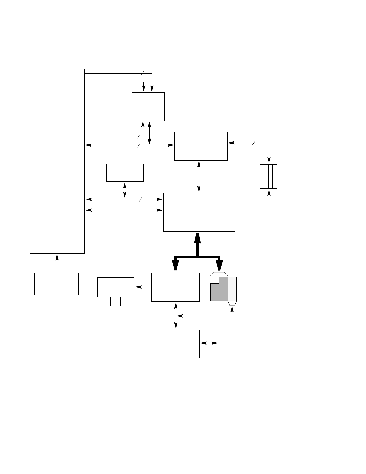
The AlphaPC 164SX is implemented in industry-standard parts and uses an Alpha
21164PC microprocessor running at 400 or 533 MHz. Figure 1–1 shows the board’s
functional components.
Page 16
1–2 Introduction
System Components and Features
Figure 1–1 AlphaPC 164SX Functional Block Diagram
Alpha 21164PC
Microprocessor
DECchip 21174-CA
Control, I/O Interface,
and Address
1MB, L2
Bcache
Quick Switches
Index
Control
18
Bcache Tag
10
128
Data
16
Address
Commands
Control
Flash ROM
128-Bit Data
168-Pin
Unbuffered
SDRAM DIMM
Sockets (× 4)
Support
– Synthesizer
PCI-to-ISA
Bridge
EIDE
Controller
Combination
Controller
Address/Control
PCI
2 Dedicated 32-Bit PCI Slots
2 Dedicated 64-Bit PCI Slots
2 Dedicated ISA Slots
Diskette
Parallel Port
2 Serial Ports
4 Devices
Page 17

Introduction 1–3
System Components and Features
1.1.1 21174 Core Logic Chip
The Alpha 21164PC microprocessor is supported by the 21174 core logic chip,
which provides an interface between three units—memory, the PCI bus, and the
21164PC (along with flash ROM). This core logic chip is the interf ace between the
21164PC microprocessor, main memory (addressing and control), and the PCI bus.
Quick switches provide the memory interface data path isolation.
The 21174 includes the majority of functions necessary to develop a high-perfor-
mance PC or workstation, requiring minimum discrete logic on the module. It provides flexible and generic functions to allow its use in a wide range of systems.
1.1.2 Memory Subsystem
The synchronous dynamic random-access memory (SDRAM) is contained in two
banks of dual inline memory modules (DIMMs). Single- or double-sided DIMMs
may be used. Two DIMMs provide 32Mb to 256MB of memory, while four DIMMs
provide up to 512MB. Table 1–1 lists the DIMM sizes tested and the corresponding
main memory si ze for 128-bit arrays.
Note: Each DIMM can be 72 bits or 64 bits wide, with 100 MHz or faster
speed.
Table 1–1 AlphaPC 164SX SDRAM Memory Configurations
(Sheet 1 of 2)
Bank 0
1
Bank 1
1
Total Memory J7 J8 J9 J10
32MB 2Mb × 72 2Mb × 72 ——
64MB 2Mb
× 72 2Mb × 72 2Mb × 72 2Mb × 72
4Mb
× 72 4M b × 72 ——
96MB 4Mb
× 72 4Mb × 72 2Mb × 72 2Mb × 72
128MB 4Mb
× 72 4Mb × 72 4Mb × 72 4Mb × 72
8Mb
× 72 8M b × 72 ——
160MB 8Mb
× 72 8M b × 72 2Mb × 72 2Mb × 72
Page 18

1–4 Introduction
System Components and Features
1.1.3 L2 Bcache Subsystem Overview
The AlphaPC 164SX board-level L2 backup cache (Bcache) is a 1MB, directmapped, synchronous, pipelined burst SROM with a 128-bit data path. The board is
capable of handling an L2 cache size of 2MB. See Section 2.3 for more information
about the Bcache.
1.1.4 PCI Interface Overview
The AlphaPC 164SX PCI interface, with a 33-MHz data transfer rate, is the main
I/O bus for the majority of functions (SCSI interface, graphics accelerator, and so
on). PCI-EIDE support is provided by an onboard controller chip (Cypress
CY82C693U-NC), which also prov ide s a PCI- to-ISA bridge, a mouse and keyboard
controller, and a time-of-year (TOY) clock.
The PCI bus has four dedicated PCI expansion slots (two 64-bit and two 32-bit).
1.1.5 ISA Interface Overview
The ISA bus provides the following system support functions:
• Two expansion slots.
• An SMC FDC37C669 combination controller chip that provides:
– A diskette controller
– Two universal asynchronous receiver-transmitters (UARTs) with full
modem control
– A bidirec t ional parallel port
1
64-bit-wide DIMMs can also be used.
Bank 0
1
Bank 1
1
Total Memory J7 J8 J9 J10
192MB 8Mb × 72 8Mb × 72 4Mb × 72 4Mb × 72
256MB 8Mb
× 72 8Mb × 72 8Mb × 72 8Mb × 72
16Mb
× 72 16Mb × 72 ——
512MB 16Mb
× 72 16Mb × 72 16Mb × 72 16Mb × 72
Table 1–1 AlphaPC 164SX SDRAM Memory Configurations
(Sheet 2 of 2)
Page 19

Introduction 1–5
Software Support
1.1.6 Miscellaneous Logic
The AlphaPC 164SX contains the following miscellaneous components:
• Operating system sup port — through a 1MB f lash ROM that contain s supporting
firmware.
• Synthesizer for clocks:
– A clock synthesizer (MC12439) provides a programmable 400- and
533-MHz cl o ck so ur ce to th e 21164PC microproce ss or. The microp roc es -
sor supplies a cl ock to the sy stem PLL/clock buffer for th e 21174.
– The 21174 core logic chip provides the SDRAM and PCI clocks.
– A 14.318-MHz crystal and frequency generator provide a clock source for
the combination controller (FDC37C669) and the PCI-to-ISA bridge
(CY82C693U-NC). The controller’s onchip generator then provides other
clocks as needed.
– A 32-kHz crystal provides the TOY clock source.
• Flash ROM:
– Fail-safe booter
– Boot code
– BIOS: Windows NT or Alpha SRM console
• Altera EPM7064LC44-7 for DMA boundary issue.
1.2 Software Support
The support elements described in this section are either included with the
AlphaPC 164SX or are available separately.
1.2.1 AlphaBIOS Windows NT Firmware
The AlphaPC 164SX motherboard ships with AlphaBIOS firmware and online documentation that describes how to configure the firmware for Windows NT. This firmware
initializes the system and enables you to install and boot the Windows NT operating
system. The AlphaBIOS firmware resides in the flash ROM on the 21A05-A0 variation
of the AlphaPC 164SX motherboard. Binary images of the AlphaBIOS firmware are
included in the motherboard Software Developer’ s Kit (SDK), along with a license
describing the terms for use and distribution.
Page 20

1–6 Introduction
Hardware Design Support
1.2.2 Alpha SRM Console Firmware
The Alpha SRM Console firmware is required to install and boot DIGITAL UNIX
on the AlphaPC 164SX. This Alpha firmware comes factory installed in the 21A05A1 variation of the AlphaPC 164SX. When installed, this firmware occupies the
flash blocks reserve d for the pri m ary firmwar e. Binary im ages of the Alpha SRM
Console firmware are included in the SDK and Firmware Update compact disk,
along with a license describing the terms for use and distribution.
1.2.3 Motherboard Software Developer’s Kit (SDK)
The SDK and Firmware Update is designed to provide an environment for developing software for Alpha mot herbo ard pr oducts . It i s als o speci ally suit ed for low-l evel
software development and hardware debug for other Alpha microprocessor-based
designs.
The following list includes some of the components of the SDK:
• The Alpha Motherboard Debug Monitor firmware with source code
• Power-up initialization SROM and SROM Mini-Debugger with source code
• Sample PALcode sources modeled after DIGITAL UNIX with source code
• Fail-safe booter with source code
• Various additional tools with source code
The following development platforms are supported by the SDK:
• DIGITAL UNIX with the C Developer’s Extensions
• Windows NT (Alpha) with the Microsoft Visual C++ Development System for
Alpha
• Windows NT (Intel) with the Microsoft Visual C++ Development System and
Tools provide limited support. This environment is currently useful for SROM
and PALcode development only.
1.3 Hardware Design Support
The full design database, including schematics and source files, is supplied. User
documentation is also included. The database allows designers with no previous
Alpha architecture experience to successfully develop a working Alpha system with
minimal assistance.
Page 21

System Configuration and Connectors 2–1
2
System Configuration and Connectors
This chapter describes the AlphaPC 164SX configuration, board connectors and
functions, and switch functions. It also identifies switch and connector locations.
The AlphaPC 164SX uses switches to implement configuration parameters such as
system speed and bo ot pa ra meters. These switches must b e con fi gur ed f or the user’s
environment. Onboard connectors are provided for the I/O interfaces, DIMMs, and
serial and parallel peripheral ports.
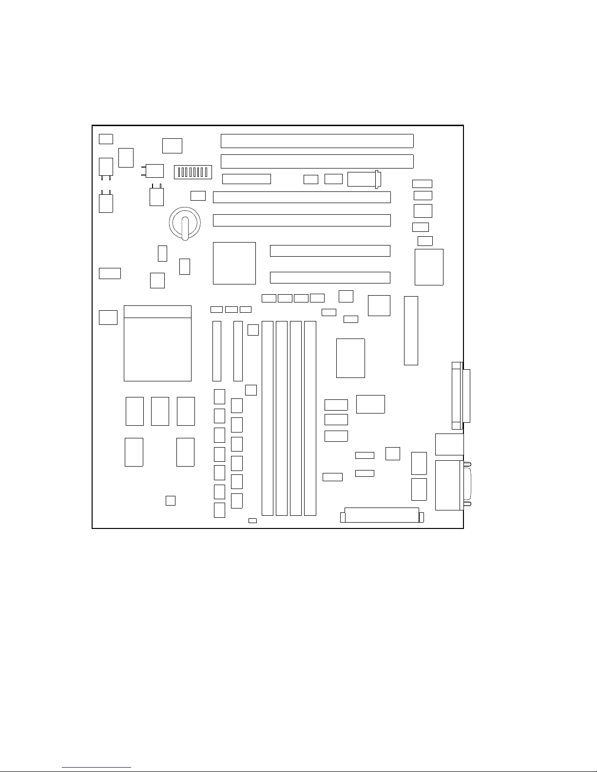
Figure 2–1 shows the board outlines and identifies the location of switches, connectors, and major components. Table 2–1 lists and defines these items.
Page 22
2–2 System Configuration and Connectors
Figure 2–1 AlphaPC 164SX Switch/Connector/Component Location
XU59
Q8
J1
J2
J3
J4
J5 J6
J7 J8 J9
J10
J11
J13
21164PC
U31
J14
J16
J15
J17
J18
J19
J20
J21
SW1 J22
J23
Q5
Q4
Q7
XB1
X2
X1
X3
U47
U39
21174
U33
U30
U46
U45
U25
U27
U23
U24
U17
U18
U12
U13
U7
U5
U3
U4
U1
U28
U32
U10 U11
U20 U21 U22
U48
U49
U50
U52
U51
U53
U54
U55
U40
U41 U42
U43
U44
U2
U8
U9
U6
U16
U14
U15
U19
U26
U29
U34
U35
U36
U37 U38
U56
Page 23

System Configuration and Connectors 2–3
Table 2–1 AlphaPC 164SX Switch/Connector/Component List
Item No. Description Item No. Description
XB1 RTC battery (CR2032) J20 LEDs/speaker/buttons connectors
J1 Soft power connector J21 SROM test port connector
J2 Input power (+3 V, +5 V, -5 V, +12 V,
-12 V)
J22 ISA slot 1
J3 COM1/COM2 (DB9) connectors J23 ISA slot 0
J4 Keyboard/mouse connectors SW1 Configuration switchpack
J5 EIDE drive 2/3 connector U48 System clock PLL (CY2081)
J6 EIDE drive 0/1 connector U10, U11,
U20, U22
L2 cache data SRAMs
J7 SDRAM DIMM 0 [0:63] connector U21 L2 cache tag SRAM
J8 SDRAM DIMM 1 [64:128] connector U33 21174 core logic chip
J9 SDRAM DIMM 2 [0:63] connector U19, U26,
U29
Memory address/control buffers
J10 SDRAM DIMM 3 [64:128] connector U1, U3, U4,
U5, U7,
U12, U13,
U17, U18,
U23, U24,
U25, U27
Data switches
J11 Diskette (floppy) drive con nector U40 to U43 Interrupt shift registers
J13 Parallel I/O connector U30 Flash ROM (1MB)
J14 Microprocessor fan/fan sense connector U46 PCI-ISA Bridge
(CY82C693U-NC)
J15 PCI slot 3 (32-bit) U36 to U38 IDE buffers
J16 Fan power, enclosure (+12 V) U47 Combination controller
(FDC37C669)
J17 PCI slot 2 (32-bit) U2, U28,
U32
Reg-reg cache isolate logic
J18 PCI slot 1 (64-bit) U31 Microprocessor, socketed
(Alpha 21164PC)
J19 PCI slot 0 (64-bit) U45 Microprocessor clock synthesizer
(MC12439)
Page 24

2–4 System Configuration and Connectors
AlphaPC 164SX Configuration Switches
2.1 AlphaPC 164SX Configuration Switches
The AlphaPC 164SX motherboa rd has a swi tchpac k locat ed at SW1, as s hown previ ously in Figure 2–1. The switches set the hardware configuration and boot options.
Figure 2–2 shows the switch functions.
Figure 2–2 AlphaPC 164SX Configuration Switches
2.2 CPU Speed Selection (CF[6:4])
The clock synthesizer at U45 makes it possible to change the frequency of the
microprocessor’s clock output. The switch configuration is set in SW1, CF[6:4].
These three switches set the speed at power-up as listed in Figure 2–2. The
microprocessor frequency divided by the ratio determines the system clock
frequency.
CF Bit: 400 MHz 533 MHz
41 1
51 0
61 1
CF0
CF1
CF2
CF3
CF4
CF5
CF6
CF7
01
Password Bypass: 0 bypasses password protection
1 requires AlphaBIOS password
Fail-Safe Booter: 0: Fail Safe
1: AlphaBIOS or SRM console
Note:
All other combinations
are reserved.
Note: Switch defaults are in bold.
Mini-Debugger: 0 enables Mini-Debugger
1 disables Mini-Debugger
CF Bit: .5MB 1M B 2MB Reserved
00 1 01
10 0 11
Page 25

System Configuration and Connectors 2–5
Bcache Size Switches (CF0 and CF1)
2.3 Bcache Size Switches (CF0 and CF1)
The Bcache size switches are located at SW1 (CF0 and CF1), as shown in
Figure 2–2. The AlphaPC 164SX is configured with 1MB of Bcache during
production; the other combinations shown in Figure 2–2 (.5MB and 2MB) are for
other implementations.
Note: The standard motherboard (21A05-A0 for Windows NT and 21A05-A1
for DIGITAL UNIX) is manufactu red wi th 64K × 32 data SSRAMs. An
OEM, however, can create an L2 cache in either a 2MB variation, using
128K × 32 data SSRAMs, or a .5MB variation, using 32K × 32 data
SSRAMs.
2.4 Password Bypass (CF2)
AlphaBIOS provides password protection. However, password bypass is provided
for system setup or startup when the AlphaBIOS password is unavailable.
Password bypass is disabled by default, with switch CF2 of SW1 in the on position
(see Figure 2–2). Whe n this functi on is enable d, it disab les the Alph aBIOS password
verification and enables the user to set up or start up their system without the
AlphaBIOS password. Password bypass also clears the password.
To disable this function and require a password, slide CF2 to the on position.
2.5 Fail-Safe Booter (CF7)
The fail-safe booter provides an emergency recovery mechanism when the primary
firmware image cont ai ned in flash memory has been corrupted. When flash memory
has been corrupted, and no image can be loaded safely from the flash, you can run
the fail-safe booter and boot another image from a diskette that is capable of reprogramming the flash.
For more information about the fail-safe booter, refer to the AlphaPC 164SX
Motherboard Windows NT User’s Manual.
Page 26

2–6 System Configuration and Connectors
Mini-Debugger (CF3)
2.6 Mini-Debugger (CF3)
The Alpha SROM Mini-Debugger is stored in the flash ROM and is enabled/
disabled by switch CF3. The default position for this switch is on (see Figure 2–2).
When this switch is off, it causes the SROM initialization to trap to the MiniDebugger after all initialization is complete, but before starting the execution of the
system flash ROM code.
2.7 AlphaPC 164SX Connector Pinouts
This section lists the pinouts of all AlphaPC 164SX connectors. See Figure 2–1 for
connector locations.
2.7.1 PCI Bus Connector Pinouts
Table 2–2 shows the PCI bus connector pinouts.
Table 2–2 PCI Bus Connector Pinouts
(Sheet 1 of 2)
Pin Signal Pin Signal Pin Signal Pin Signal
32-Bit and 64-Bit PCI Connectors (J15, J17, J18, J19)
A1 TRST# A2 +12V A3 TMS A4 TDI
A5 Vdd A6 INTA A7 INTC A8 Vdd
A9 —A10Vdd A11 — A12 Gnd
A13 Gnd A14 — A15 RST# A16 Vdd
A17 GNT# A18 Gnd A19 — A20 AD[30]
A21 +3V A22 AD[28] A23 AD[26] A24 Gnd
A25 AD[24] A26 IDSEL A27 +3V A28 AD[22]
A29 AD[20] A30 Gnd A31 AD[18] A32 AD[16]
A33 +3V A34 FRAME# A35 Gnd A36 TRDY#
A37 STOP# A38 STOP# A39 +3V A40 SDONE
A41 SBO# A42 Gnd A43 PAR A44 AD[15]
A45 +3V A46 AD[13] A47 AD[11] A48 Gnd
A49 AD[09] A50 Not used A51 Not used A52 C/BE#[0]
A53 +3V A54 AD[06] A55 AD[04] A56 Gnd
A57 AD[02] A58 AD[00] A59 Vdd A60 REQ64#
A61 Vdd A62 Vdd B1 -12V B2 TCK
B3 Gnd B4 TDO B5 Vdd B6 Vdd
B7 INTB B8 INTD B9 PRSNT1# B10 —
B11 PRSNT2# B12 Gnd B13 Gnd B14 —
Page 27

System Configuration and Connectors 2–7
AlphaPC 164SX Connector Pinouts
B15 Gnd B16 CLK B17 Gnd B18 REQ#
B19 Vdd B20 AD[31] B21 AD[29] B22 Gnd
B23 AD[27] B24 AD[25] B25 +3V B26 C/BE#[3]
B27 AD[23] B28 Gnd B29 AD[21] B30 AD[19]
B31 +3V B32 AD[17] B33 C/BE#[2] B34 Gnd
B35 IRDY# B36 +3V B37 DEVSEL# B38 Gnd
B39 LOCK# B40 PERR# B41 +3V B42 SERR#
B43 +3V B44 C/BE#[1] B45 AD[14] B46 Gnd
B47 AD[12] B48 AD[10] B49 Gnd B50 Not used
B51 Not used B52 AD[08] B53 AD[07] B54 +3V
B55 AD[05] B56 AD[03] B57 Gnd B58 AD[01]
B59 Vdd B60 ACK64# B61 Vdd B62 Vdd
64-Bit PCI Connectors Only (J18, J19)
A63 Gnd A64 C/BE#[7] A65 C/BE#[5] A66 Vdd
A67 PAR64 A68 D[62] A69 Gnd A70 D[60]
A71 D[58] A72 Gnd A73 D[56] A74 D[54]
A75 Vdd A76 D[52] A77 D[50] A78 Gnd
A79 D[48] A80 D[46] A81 Gnd A82 D[44]
A83 D[42] A84 Vdd A85 D[40] A86 D[38]
A87 Gnd A88 D[36] A89 D[34] A90 Gnd
A91 D[32] A92 —A93Gnd A94 —
B63 — B64 Gnd B65 C/BE#[6] B66 C/BE#[4]
B67 Gnd B68 D[63] B69 D[61] B70 Vdd
B71 D[59] B72 D[57] B73 Gnd B74 D[55]
B75 D[53] B76 Gnd B77 D[51] B78 D[49]
B79 Vdd B80 D[47] B81 D[45] B82 Gnd
B83 D[43] B84 D[41] B85 Gnd B86 D[39]
B87 D[37] B88 Vdd B89 D[35] B90 D[33]
B91 Gnd B92 — B93 — B94 Gnd
Table 2–2 PCI Bus Connector Pinouts
(Sheet 2 of 2)
Pin Signal Pin Signal Pin Signal Pin Signal
Page 28

2–8 System Configuration and Connectors
AlphaPC 164SX Connector Pinouts
2.7.2 ISA Expansion Bus Connector Pinouts
Table 2–3 shows the ISA expansion bus connector pinouts.
Table 2–3 ISA Expansion Bus Connector Pinouts (J22, J23)
Pin Signal Pin Signal Pin Signal Pin Signal
1 Gnd 2 IOCHCK# 3 RSTDRV 4 SD7
5 Vdd 6 SD6 7 IRQ9 8 SD5
9 –5V 10 SD4 11 DRQ2 12 SD3
13 –12V 14 SD2 15 ZEROWS# 16 SD1
17 +12V 18 SD0 19 Gnd 20 IOCHRDY
21 SMEMW# 22 AEN 23 SMEMR# 24 SA19
25 IOW# 26 SA18 27 IOR# 28 SA17
29 DACK3# 30 SA16 31 DRQ3 32 SA15
33 DACK1# 34 SA14 35 DRQ1 36 SA13
37 REFRESH# 38 SA12 39 SYSCLK 40 SA11
41 IRQ7 42 SA10 43 IRQ6 44 SA9
45 IRQ5 46 SA8 47 IRQ4 48 SA7
49 IRQ3 50 SA6 51 DACK2# 52 SA5
53 TC 54 SA4 55 BALE 56 SA3
57 Vdd 58 SA2 59 OSC 60 SA1
61 Gnd 62 SA0 63 MEMCS16# 64 SBHE#
65 IOCS16# 66 LA23 67 IRQ10 68 LA22
69 IRQ11 70 LA21 71 IRQ12 72 LA20
73 IRQ15 74 LA19 75 IRQ14 76 LA18
77 DACK0# 78 LA17 79 DRQ0 80 MEMR#
81 DACK5# 82 MEMW# 83 DRQ5 84 SD8
85 DACK6# 86 SD9 87 DRQ6 88 SD10
89 DACK7# 90 SD11 91 DRQ7 92 SD12
93 Vdd 94 SD13 95 MASTER# 96 SD14
97 Gnd 98 SD15 —— ——
Page 29

System Configuration and Connectors 2–9
AlphaPC 164SX Connector Pinouts
2.7.3 SDRAM DIMM Connector Pinouts
Table 2–4 shows the SDRAM DIMM connector pinouts.
Table 2–4 SDRAM DIMM Connector Pinouts (J7 through J10)1
(Sheet 1 of 2)
Pin Signal Pin Signal Pin Signal Pin Signal
1 Gnd 2 DQ0 3 DQ1 4 DQ2
5 DQ3 6 +3V 7 DQ4 8 DQ5
9 DQ6 10 DQ7 11 DQ8 12 Gnd
13 DQ9 14 DQ10 15 DQ11 16 DQ12
17 DQ13 18 +3V 19 DQ14 20 DQ15
21 CB0 22 CB1 23 Gnd 24 NC
25 NC 26 +3V 27 WE
28 DQMB0
29 DQMB1 30 S0
31 NC 32 Gnd
33 A0 34 A2 35 A4 36 A6
37 A8 38 A10 39 A12 40 +3V
41 +3V 42 CK0 43 Gnd 44 NC
45 S2
46 DQMB2 47 DQMB3 48 NC
49 +3V 50 NC 51 NC 52 CB2
53 CB3 54 Gnd 55 DQ16 56 DQ17
57 DQ18 58 DQ19 59 +3V 60 DQ20
61 NC 62 NC 63 CKE1 64 Gnd
65 DQ21 66 DQ22 67 DQ23 68 Gnd
69 DQ24 70 DQ25 71 DQ26 72 DQ27
73 +3V 74 DQ28 75 DQ29 76 DQ30
77 DQ31 78 Gnd 79 CK2 80 NC
81 NC 82 SDA 83 SCL 84 +3V
85 Gnd 86 DQ32 87 DQ33 88 DQ34
89 DQ35 90 +3V 91 DQ36 92 DQ37
93 DQ38 94 DQ39 95 DQ40 96 Gnd
97 DQ41 98 DQ42 99 DQ43 100 DQ44
101 DQ45 102 +3V 103 DQ46 104 DQ47
105 CB4 106 CB5 107 Gnd 108 NC
109 NC 110 +3V 111 CAS
112 DQMB4
113 DQMB5 114 S1 115 RAS
116 Gnd
117 A1 118 A3 119 A5 120 A7
121 A9 122 BA0 123 A13 124 +3V
Page 30

2–10 System Configuration and Connectors
AlphaPC 164SX Connector Pinouts
2.7.4 EIDE Drive Bus Connector Pinouts
Table 2–5 shows the EIDE drive bus connector pinouts.
1
Pins 1 through 84 are on the front side and pins 85 through 168 are on the back side.
2
The AlphaPC 164SX uses BA1 as both BA1 and ADDR12. Therefore, four-bank DIMMs using ADDR[11:0]
are the maximum size. (Two-bank DIMMs can use ADDR[12:0].)
3
Pull-down.
125 CK1 126 BA1
2
127 Gnd 128 CKE0
129 S3
130 DQMB6 131 DQMB7 132 PD
3
133 +3V 134 NC 135 NC 136 CB6
137 CB7 138 Gnd 139 DQ48 140 DQ49
141 DQ50 142 DQ51 143 +3V 144 DQ52
145 NC 146 NC 147 PD 148 Gnd
149 DQ53 150 DQ54 151 DQ55 152 Gnd
153 DQ56 154 DQ57 155 DQ58 156 DQ59
157 +3V 158 DQ60 159 DQ61 160 DQ62
161 DQ63 162 Gnd 163 CK3 164 NC
165 SA0 166 SA1 167 SA2 168 +3V
Table 2–5 EIDE Drive Bus Connector Pinouts (J5, J6)
Pin Signal Pin Signal Pin Signal Pin Signal
1 RESET 2 Gnd 3 IDE_D7 4 IDE_D8
5 IDE_D6 6 IDE_D9 7 IDE_D5 8 IDE_D10
9 IDE_D4 10 IDE_D11 11 IDE_D3 12 IDE_D12
13 IDE_D2 14 IDE_D13 15 IDE_D1 16 IDE_D14
17 IDE_D0 18 IDE_D15 19 Gnd 20 NC (key pin)
21 MARQ 22 Gnd 23 IOW
24 Gnd
25 IOR
26 Gnd 27 CHRDY 28 BALE
29 MACK 30 Gnd 31 IRQ 32 IOCS16
33 ADDR1 34 NC 35 ADDR0 36 ADDR2
37 CS0
38 CS1 39 ACT 40 Gnd
Table 2–4 SDRAM DIMM Connector Pinouts (J7 through J10)
1
(Sheet 2 of 2)
Pin Signal Pin Signal Pin Signal Pin Signal
Page 31

System Configuration and Connectors 2–11
AlphaPC 164SX Connector Pinouts
2.7.5 Diskette (Floppy) Drive Bus Connector Pinouts
Table 2–6 shows the diskette (floppy) drive bus connector pinouts.
2.7.6 Parallel Bus Connector Pinouts
Table 2–7 shows the parallel bus connector pinouts.
Table 2–6 Diskette (Floppy) Drive Bus Connector Pinouts (J11)
Pin Signal Pin Signal Pin Signal Pin Signal
1 Gnd 2 DEN0 3 Gnd 4NC
5Gnd 6 DEN1 7 Gnd 8 INDEX
9 Gnd 10 MTR0 11 Gnd 12 DR1
13 Gnd 14 DR0 15 Gnd 16 MTR1
17 Gnd 18 DIR 19 Gnd 20 STEP
21 Gnd 22 WDATA 23 Gnd 24 WGATE
25 Gnd 26 TRK0 27 Gnd 28 WRTPRT
29 ID0 30 RDATA 31 Gnd 32 HDSEL
33 ID1 34 DSKCHG —— — —
Table 2–7 Parallel Bus Connector Pinouts (J13)
Pin Signal Pin Signal Pin Signal Pin Signal
1 STB 2 PD0 3 PD1 4 PD2
5 PD3 6 PD4 7 PD5 8 PD6
9 PD7 10 ACK 11 BUSY 12 PE
13 SLCT 14 AFD 15 ERR 16 INIT
17 SLIN 18 Gnd 19 Gnd 20 Gnd
21 Gnd 22 Gnd 23 Gnd 24 Gnd
25 Gnd —— —— — —
Page 32

2–12 System Configuration and Connectors
AlphaPC 164SX Connector Pinouts
2.7.7 COM1/COM2 Serial Line Connector Pinouts
Table 2–8 shows the COM1/COM2 serial line connector pinouts.
2.7.8 Keyboard/Mouse Connector Pinouts
Table 2–9 shows the keyboard/mouse connector pinouts.
Table 2–8 COM1/COM2 Serial Line Connector Pinouts (J3)
COM1 Pin
(Top) COM1 Signal
COM2 Pin
(Bottom) COM2 Signal
1 DCD1 1 DCD2
2 RxD1 2 RxD2
3 TxD1 3 TxD2
4 DTR1 4 DTR2
5 SG1 5 SG2
6 DSR1 6 DSR2
7 RTS1 7 RTS2
8 CTS1 8 CTS2
9 RI1 9 RI2
Table 2–9 Keyboard/Mouse Connector Pinouts (J4)
Keyboard Pin
(Top) Keyboard Signal
Mouse Pin
(Bottom) Mouse Signal
1 KBDATA 1 MSDATA
2NC 2NC
3Gnd 3 Gnd
4 Vdd 4 Vdd
5 KBCLK 5 MSCLK
6NC 6NC
Page 33

System Configuration and Connectors 2–13
AlphaPC 164SX Connector Pinouts
2.7.9 SROM Test Data Input Connector Pinouts
Table 2–10 shows the SROM test data input connector pinouts.
2.7.10 Input Power Connector Pinouts
Table 2–11 shows the input power connector pinouts.
2.7.11 Enclosure Fan Power Connector Pinouts
Table 2–12 shows the enclosure fan power connector pinouts.
1
This pinout is ATX-compliant.
Table 2–10 SROM Test Data Input Connector Pinouts (J21)
Pin Signal Description
1NC —
2SROM_CLK_L Clock out
3 Gnd —
4NC —
5TEST_SROM_D_L SROM serial data in
6NC —
Table 2–11 Input Power Connector Pinouts (J2)
1
Pin Voltage Pin Voltage Pin Voltage Pin Voltage
1 +3.3 V dc 2 +3.3 V dc 3 Gnd 4+5 V dc
5Gnd 6+5 V dc7 Gnd 8 P_DCOK
9 5 V SB 10 +12 V dc 11 +3.3 V dc 12 –12 V dc
13 Gnd 14 PS_ON 15 Gnd 16 Gnd
17 Gnd 18 –5 V dc 19 +5 V dc 20 +5 V dc
Table 2–12 Enclosure Fan (+12 V dc) Power Connector Pinouts (J16)
Pin Voltage
1 Gnd
2 +12 V dc
3 Gnd
Page 34

2–14 System Configuration and Connectors
AlphaPC 164SX Connector Pinouts
2.7.12 Microprocessor Fan Power Connector Pinouts
Table 2–13 shows the microprocessor fan power connector pinouts.
2.7.13 Soft Power Connector Pinouts
Table 2–14 shows the soft power connector pinouts.
2.7.14 Multipurpose Connector Pinouts
J20 is a multipurpose connector that provides pins for the following functions:
• System speaker
• LEDs for power and the EIDE drive
• Buttons for reset and halt
Table 2–15 shows the multipurpose connector pinouts, and Figure 2–3 shows the
connector layout.
Table 2–13 Microprocessor Fan Power Connector Pinouts (J14)
Pin Signal Description
1 +12 V dc —
2 FAN_CONN_L Fan connected
3 Gnd —
Table 2–14 Soft Power Connector Pinouts (J1)
Pin Signal Description
1 Input System power on/off
2 Gnd —
Table 2–15 Multipurpose Connector Pinouts (J20)
(Sheet 1 of 2)
Pin Signal Description
1 Gnd —
2 HALT_BUTTON
1
Halt system
3 Gnd —
4 RESET_BUTTON Reset system
5 HD_PU Hard drive power-up
6 HD_LED Pull-up to Vdd
Page 35

System Configuration and Connectors 2–15
AlphaPC 164SX Connector Pinouts
Figure 2–3 Multipurpose Connector Pinouts
1
The halt button is not used with the Windows NT operating system.
7 — No connection
8 POWER_LED_L Pull-up to Vdd
10, 12, 14, 16 Gnd —
9 SPKR Speaker output
15 Vdd —
11, 13 — No connection
Table 2–15 Multipurpose Connector Pinouts (J20)
(Sheet 2 of 2)
Pin Signal Description
12
3
4
56
78
910
11 12
13 14
15 16
HALT_BUTTON
(See note.)
RESET_BUTTON
HD_LED
POWER_LED_L
HD_PU
SPKR
Vdd
Note: The halt button is not used with Windows NT.
J20
Page 36

Page 37

Power and Environmental Requirements 3–1
3
Power and Environmental Requirements
This chapter describes the AlphaPC 164SX power and environmental requirements,
and physical board parameters.
3.1 Power Requirements
The AlphaPC 164SX derives its main dc power from a user-suppli ed power supply.
The board has a total power dissipation of 90 W, excluding any plug-in PCI and I S A
devices. An onboard +5-V t o +2.5- V dc- to- dc con verter is designed to handle 24 A o f
current. Table 3–1 lists the power requi rement for eac h dc s uppl y voltage.
The power supply must supply a dcok signal to the system reset logic. Refer to
Section 4.6 for additional information.
Caution: Fan sensor required. The 21164PC microprocessor cooling fan must
drive an RPM indicator signal. If the airflow stops, the sensor on the
motherboard detects that the RPM has stopped, and resets the system.
1
Values indicated are for an AlphaPC 164SX motherboard with an Alpha 21164PC microprocessor operating at 533 MHz, with 128MB SDRAM, excluding adap ter cards and disk drives.
Table 3–1 Power Supply DC Current Requirements
Voltage/Tolerance Current
1
+3.3 V dc, ±5% 5.0 A
+5 V dc,
±5% 12.0 A
–5 V dc,
±5% 0.0 A
+12 V dc,
±5% 1.0 A
–12 V dc,
±5% 100.0 mA
Page 38

3–2 Power and Environmental Requirements
Environmental Requirements
3.2 Environmental Requirements
The 21164PC microprocessor is cooled by a small fan blowing directly into the
chip’s heat sink. The AlphaPC 164SX motherboard is designed to run efficiently by
using only this f an. Add it ion al fans may be necessary depending upon cabin et ry a nd
the requirements of plug-in cards.
The AlphaPC 164SX motherboard is specified to run within the environment listed
in Table 3–2.
3.3 Board Dimensions
The AlphaPC 164SX is an ATX-size printed-wiring board (PWB) with the following
dimensions:
• Length: 30.48 cm (12.0 in ±0.0005 in)
• Width: 24.38 cm (9.6 in ±0.0005 in)
• Height: 6.00 cm (2.4 in)
The board can be used in certain desktop and deskside systems that have adequate
clearance for the 21164PC heat sink and its cooling fan. All ISA and PCI expansion
slots are usable in standard desktop or deskside enclosures.
Table 3–2 AlphaPC 164SX Motherboard Environmental Requirements
Parameter Specification
Operating temperature 10°C to 40°C (50°F to 104°F)
Storage temperature –55°C to 125°C (–67°F to 257°F)
Relative humidity 10% to 90% with maxi mum wet bulb temperature 28°C
(82°F) and minimum dew point 2°C (36°F)
Rate of (dry bulb) temperature
change
11°C/hour
±2°C/hour (20°F/hour ±4°F/hour)
Page 39

Power and Environmental Requirements 3–3
Board Dimensions
3.3.1 ATX Hole Specification
Figure 3–1 shows the ATX hole specification for the AlphaPC 164SX.
Figure 3–1 ATX Hole Specification
.800
TYP Between
Connectors
.650
.500
.400
4.900
1.612
.600
.625
9.600
8.950
6.100
ISA Connector
(2 Places)
PCI Connector
(4 Places)
1.300
11.100
12.000
FM-06122.AI4
Page 40

3–4 Power and Environmental Requirements
Board Dimensions
3.3.2 ATX I/O Shield Requirements
Figure 3–2 shows the ATX I/O shield dimensions for the AlphaPC 164SX.
Figure 3–2 ATX I/O Shield Dimensions
11.15
15.47
4.35
17.95
22.95
23.96
29.10
33.10
9.25
3.58
2.45
5.00 TYP
R 1.00
21.36
16.05
68.4
64.9
24.7
16.7
35.5
43.5
74.8
78.2
85.4
87.2
94.4
98.9
64.91
60.26
51.27
42.28
40.48
34.13
25.14
16.15
14.35
8.00
0.99
9.98
11.78
18.13
19.93
28.92
37.91
44.26
46.06
55.05
64.04
70.39
72.19
81.18
90.17
95.40
14.96
R 1.00
7.19 TYP
FM-05986.AI4
Page 41

Functional Description 4–1
4
Functional Description
This chapter describes the functional operation of the AlphaPC 164SX. The description introduces the 21174 core logic chip and describes its implementation with the
2116 4PC microproce ssor , it s support ing memory, and I/O devices. Figure 1–1 s hows
the AlphaPC 164SX major functional components.
Bus timing and protocol information found in other data sheets and reference documentation is not duplicated. See Appendix A for a list of supporting documents and
order numbers.
Note: For detailed descriptions of bus transactions, chip logic, and operation,
refer to the Alpha 21164PC Microprocessor Hardware Reference Manual and the 21174 Core Logic Chip Technical Reference Manual. For
details of the PCI interface, refer to the PCI System Design Guide.
Page 42

4–2 Functional Description
AlphaPC 164SX Bcache Interface
4.1 AlphaPC 164SX Bcache Interface
The 21164PC microprocessor controls the board-level L2 backup cache (Bcache)
array (see Figure 4–1). The dat a bus ( data_h[1 27:0]) signals are sh are d with the system interface.
Figure 4–1 AlphaPC 164SX L2 Bcache Array
The Bcache is a 1MB , direct -mapped, pipelined , synchron ous burs t SRAM
(SSRAM) with a 128-b it data path . It is populated with a quantity of four
133-MHz, 64K × 32 SSRAM s for data stor e, and on e 133-MHz , 32K × 32
SSRAM for tag sto re. The Bca che supp orts 64-by te transfe rs to and from
memory.
data_ram_oe_h
21164PC
Microprocessor
Bcache
SRAM
index_h[21:4]
data_ram_we_h
tag_ram_oe_h
tag_ram_we_h
index_h[21:6]
tag_data_h[32:30],19
tag_data_h[29:20]
tag_data_par_h
tag_valid_h
tag_dirty_h
data_h[127:0]
st_clk
x
_h
idle_bc_h
fill_dirty_h
Tag
Array
Data
Array
21174
Page 43

Functional Description 4–3
21174 Core Logic Chip
4.2 21174 Core Logic Chip
The 21174 core lo g i c c hi p pr o v id e s a cost-compe t it i ve s o lu t io n fo r d es i gn er s u s in g t h e
21164PC microprocessor to develop unipr oces sor syst ems. The chip provides a
128-bit memory interface and a PCI I/O interface, and i nclu des t he 21174-CA chip
packaged in a 474-pin p las ti c bal l gr id a rr ay (PBGA).
Figure 4–2 shows the AlphaPC 164SX implementation of the 21174 core logic chip.
Figure 4–2 Main Memory Interface
4.2.1 21174 Chip Overview
The 21 174 ap plication-specific int egrated circuit (ASIC) acc ept s add res se s and commands from the 21 164PC microproc essor and drive s the main memory array with the
address, contro l, and cloc k sign als. It also pro vid es an inte rfac e to the 64- bit PCI I/O
bus.
21164PC
data_h[127:0]
addr_h[39:4]
System Control
*
DIMM 0
DIMM 1
DIMM 2
DIMM 3
Quick
Switches
21174
Buffers
memadr_[13:0]
mem_dat[128:0]
bnmemadr[13:0]
memwe_l
memcas_l[7:0]
memrasb_l[7:0]
memrasa_l[7:0]
miscellaneous
bnmemwe_l
bnmemcas_l[7:0]
bnmemrasb_l[7:0]
bnmemrasa_l[7:0]
bnmiscellaneous
be_l[0:2]
64-Bit PCI
I/O Bus
addr_bus_req_h
addr_cmd_par_h
cack_h
cmd_h[3:0]
dack_h
fill_h
fill_dirty_h
fill_error_h
fill_id_h
idle_bc_h
int4_valid_h[3:0]
sys_reset_l
tag_dirty_h
victim_pending_h
*
Page 44

4–4 Functional Description
21174 Core Logic Chip
The 21174 chip provides the following functions:
• Serves as the interface between the 21164PC microprocessor, main memory
(addressing and control), and the PCI bus. A three-entry CPU instruction queue
is implemented to capture commands should the memory or I/O port be busy.
• Provides control to the Quick Switch chips to isolate the L2 cache from the main
memory bus during private reads and writes.
• Generates the clocks, row, and column addresses for the SDRAM DIMMs, as
well as all of the memory control signals (RAS, CAS, WE). All of the required
SDRAM refresh control is contained in the 21174.
• Provides all the logic to map 21164PC noncacheable addresses to PCI address
space, as well as all the translation logic to map P CI DMA add resses to system
memory.
Two DMA conversion methods are supported:
• Direct mapping, in which a base offset is concatenated with the PCI address.
• Scatter-gather mapping, which maps an 8KB PCI page to any 8KB memory
page. The 21174 contains an eight-entry scatter-gather translation lookaside
buffer (TLB) , wh ere each entry holds f our c onse cut ive page table ent ri es (PTEs).
4.2.2 Main Memory Interface
Quic k Sw it che s p rov id e t he i nt er fac e be tw een th e 21164PC/L2 cac he (data_h[127:0])
and the memory/21174 (mem_data_h[127:0 ]). The AlphaPC 164SX supports four
168-pin unbuf fered 72-bit or 64-bi t SDRAM DIMM modules. Even parity i s generated
on the PCI bus.
The AlphaPC 164SX supports a maximum of 512MB of mai n memory. The memory
is organize d as two banks. Table 1–1 lists total memory option s al ong with the corresponding DIMM sizes r equired. All CPU c acheab le memory acce sses and PCI DMA
accesses are controlled and routed to main memory by the 21174 core logic chip.
The AlphaPC 164SX implements the alternate memory mode for SDRAM RAS
and CAS control signals. Alternate memory mode is explained in the 21174 Core
Logic Chip Technical Reference Manual.
Page 45

Functional Description 4–5
21174 Core Logic Chip
4.2.3 PCI Devices
The AlphaPC 164SX uses the PCI bus as t he main I/ O bus for the majorit y of per iph-
eral functions. As Figure 4–3 shows, the board implements the ISA bus as an expansion bus for system support functions and for relatively slow peripheral devices.
Figure 4–3 AlphaPC 164SX PCI Bus Devices
The PCI bus supports multiplexed, burst mode, read and w rite transfers. It supports synchronous operation of 33 MHz. It also supports either a 32 -bit or 64-bit
data path with 32-bit device support in the 64-bit configuration. Depending upo n
the configuration and operating frequencies, the PCI bus supports up to 264-MB/s
(33 MHz, 64-bit) peak throughput. The PCI p rovides parity on address and data
cycles. Three physical address spaces are supported:
• 32-bit memory space
• 32-bit I/O space
• 256-byte-per-agent configuration space
2117 4
CY82C693U-NC
Primary
J6
Secondary
J5
ISA EIDE
PCI
Slot 0
J19
PCI
Slot 1
J18
PCI
Slot 2
J17
PCI
Slot 3
J15
PCI
ISA Bus
Device IDSEL Select
Slot 2 16
Slot 0 17
Slot 1 18
PCI/ISA Bridge 19
Slot 3 20
Page 46

4–6 Functional Description
ISA Bus Devices
The bridge from the 21164PC system bus to the 64-bit PCI bus is provided by the
21174 chip. It generates the required 32-bit PCI address for 21164PC I/O accesses
directed to the PCI. It also accepts 64-bit double address cycles and 32-bit single address
cycles. However, the 64-bit address support is subject to some constraints.
4.2.4 PCI/ISA Bridge Chip
The CY82C693U-NC chip provides the bridge between the PCI and the ISA bus,
and between the PCI and the EIDE bus. It also incorporates the logic for the following:
• Keyboard/mouse controller – An 8042-compatible interface is brought out to
separate 6-pin DIN connectors (J4).
• Real-time clock – A DS1287-compatible clock is backed up by a replaceable
battery (XB1).
• A PCI interface (master and slave).
• An ISA interface (master and slave).
• PCI and ISA arbitration.
Refer to the Cypress document CY82C693U hyperCache/Stand-Alone PCI
Peripheral Controller with USB Data Sheet for additional information.
4.2.5 PCI Expansion Slots
Four dedicated PCI expansion slots are provided on the AlphaPC 164SX. This
allows the system user to add addit ional 32-bit or 64-bit PCI options. Whil e both the
32-bit and the 64-bit slots use the standard 5-V PCI connector and pinout, +3.3 V is
supplied for those boards that require it. The CY82C693U-NC chip provides the
interface to the ISA expansion I/O bus.
4.3 ISA Bus Devices
Figure 4–4 shows the AlphaPC 164SX ISA bus implementation with peripheral
devices and connectors. Two dedicated ISA expansion slots are provided. System
support features such as serial lines, parallel port, and diskette controller are embedded on the module by means of an FDC37C669 combination controller chip.
Page 47

Functional Description 4–7
ISA Bus Devices
4.3.1 Combination Controller Chip
The AlphaPC 164SX uses the Standard Microsystems Corporation FDC37C669
combination controller chip (see Figure 4–4). It is packaged in a 100-pin QFP configuration. The chip provides the following ISA peripheral functions:
• Diskette controller – Software compatible to the Intel N82077 FDC. Inte-
grates the fu n ctio n s o f the f or mat te r/ co nt roll er, digita l d ata se p ar at or, write
precompen sa ti on , an d da ta -ra te sele ct io n l ogic re qu irin g no ex te rn al filte r
components. Supports the 2.88-MB drive format and other standard diskette
drives used with 5.25-inch and 3.5-inch media. FDC data and control lines are
brought out to a sta ndard 34-pin connector (J1 1). A ribbon cable in terfaces the
connector to one or two diskette drives.
• Serial ports – Two UARTs with full modem control, compatible with NS16450
or PC16550 devices, are brought out to two separate onboard, 9-pin
D-subminiature connectors (J3).
• Parallel port – The bidirectional parallel port is brought out to an onboard
25-pin connector (J13). It can be brought out through a 25-pin female
D-subminiature connector on the bulkhead of a standard PC enclosure.
An onboard clock generator chip supplies a 14.3-MHz reference clock for the diskette data separator and serial ports.
Page 48

4–8 Functional Description
ISA Bus Devices
Figure 4–4 AlphaPC 164SX ISA Bus Devices
4.3.2 ISA Expansion Slots
Two ISA expansion slots are provided for plug-in ISA peripherals (J22 and J23).
4.3.3 ISA I/O Address Map
Table 4–1 lists the AlphaPC 164SX ISA I/O space address mapping.
Table 4–1 ISA I/O Address Map
(Sheet 1 of 2)
Range (hex) Usage
000-00F 8237 DMA #1
020-021 8259 PIC #1
040-043 8253 timer
060-061 Ubus IRQ12 and NMI control
sd[7:0]
PCI-to-ISA
Bridge
CY82C693U-NC
la[23:17]
PCI
sd[15:0]
Combination
Controller
37C669
Diskette
Parallel
COM1/2
ISA0
ISA1
sa[19:0]
sa[15:0]
Transceivers
EIDE – Primary
EIDE – Sec ondary
Page 49

Functional Description 4–9
Interrupts
4.3.4 Flash ROM Address Map
After reset, the flash ROM is set to location 0. The 21174 supports cache fills and
uncacheable reads from the flash ROM (that is, the 21174 does multiple reads to the
flash ROM to assemble full octawords). The 21164PC can start executing directly
from the flash ROM.
Once the boot code that was stored in the flash ROM has been executed, and memory has been initialized, the flash ROM is mapped to locations
87.C000.000–87.FFFF.FFFF.
4.4 Interrupts
Interrupts and general-purpose inputs are acquired by the 21174 through a freerunning 32-bit external shift register. The int_sr_ load_l s ignal is asse rted low to load
the interrupts into the shift register. The int_clk signal clocks the shift register contents into the 21174 through the int_sr_in pin. The shift register operates continuously at a rate of ¼ the chipset clock rate .
The state of each interrupt can be read through the interrupt request register. Note
that the state of the interrupts will pers ist in the interrupt request register fo r up to
3 µs after t he interrupt has been deasserted a t the shift re gister. If the interrupt bit in
the interrupt request register is not promptly cleared, a second interrupt might be
taken before the shift register scans the deasserted value into the interrupt request
070 CMOS RAM address and NMI mask register
080-08F DMA page registers
0A0-0A1 8259 PIC #2
0C0-0DF 8237 DMA #2
2F8-2FF Serial port—COM2
370-377 Secondary diskette (floppy)
3BC-3BF Parallel port—LPT1
3F0-3F7 Primary diskette (floppy)
3F8-3FF Serial port—COM1
Table 4–1 ISA I/O Address Map
(Sheet 2 of 2)
Range (hex) Usage
Page 50

4–10 Functional Description
Interrupts
register. Interrupts latched in the interrupt request register can be reset individually
by writing a 1 to the bit to be cleared. This immediately cl ear s the bit to avoi d taking
a second interrupt. Figure 4–5 shows the interrupt request register.
Figure 4–5 Interrupt Request Register
The interrupt mask register provides individual mask bits for each interrupt.
Table 4–2 lists the AlphaPC 164SX system interrupts, and Table 4–3 lists the ISA
interrupts.
1
IPL = interrupt priority level (fixed)
Table 4–2 AlphaPC 164SX System Interrupts
21164PC Interrupt IPL
1
Suggested Usage AlphaPC 164SX Usage
cpu_irq[0] 20 Corrected system error Reserved
cpu_irq[1] 21 — PCI and ISA interrupts
cpu_irq[2] 22 Interprocessor and
timer interrupts
TOY clock interrupt
cpu_irq[3] 23 — Reserved
pwr_fail_irq 30 Powerfail interrupt Reserved
sys_mch_chk_irq 31 System machine check
interrupt
NMI and 21174 errors
mch_hlt_irq — Halt Reserved
31 24 23 20 19 16 15 12 11 08 07 06 05 03 02 01 00
63 62
A2 A3A1A0B2 B3B1B0
C2 C3C1C0D2 D3D1D0
06 07050402 030100
Reserved
NMI INT
Halt INT
Reserved
Real-time CLK_INT
ISA_INT
PCI_INT A
n
PCI_INT B
n
PCI_INT C
n
PCI_INT D
n
CONFIG[7:0]
Reserved
21174 CLK_INT
ERROR INT
61 32
Page 51

Functional Description 4–11
Interrupts
1
The # symbol indicates an active low signal.
Table 4–3 ISA Interrupts
Interrupt
Number Interrupt Source
IRQ0 Internal timer
IRQ1 Keyboard
IRQ2 Interrupt from controller 2
IRQ3 COM2
IRQ4 COM1
IRQ5 Available
IRQ6 Diskette (floppy)
IRQ7 Parallel port
IRQ8#
1
Reserved
IRQ9 Available
IRQ10 USB
IRQ11 Available
IRQ12 Mouse
IRQ13 Available
IRQ14 EIDE
IRQ15 EIDE
Page 52

4–12 Functional Description
System Clocks
4.5 System Clocks
Figure 4–6 shows the AlphaPC 164SX clock generation and distribution scheme.
The AlphaPC 164SX system includes input clocks to the microprocessor as well as
clock distribution for the various system memory and I/O devices. There are other
miscellaneous clocks for ISA bus support. System clocking can be divided into the
following three main areas:
• Microproc essor inp ut clock — The input clock r uns at the operating fr equency
of the 21 16 4PC microp rocess or. The AlphaPC 164SX supports c ycle time s from
2.50 ns to 1.88 ns. This implies input clock frequencies from 400 MHz to
533 MHz. The clock is provid ed by using a s ynthesize r. The synthesizer’s o utput
is used as the input clock for the 21164PC.
• Clock distribution — Clock dist ri bution includes the dist rib ution of system
clocks from the 21164PC microprocessor to t he sys tem l ogic. The AlphaPC
164SX clock distribution scheme is flex ible enoug h to allow t he majo rity of c ycletime combinations to be supported. Because the PCI is synchr onous to t he system
clock generated by the 21164PC microprocessor, the PCI cyc le t ime i s a mul ti ple
of th e 21164PC cycle time. This distribution scheme supports a PCI operation of
33 MHz.
• Miscella neous clocks — The miscellaneous clocks include those needed for
ISA and the co mbinati on cont roll er. These clocks are pr ovide d by a cryst al a nd a
frequency generator with fixed scaling.
Page 53

Functional Description 4–13
System Clocks
Figure 4–6 AlphaPC 164SX System Clocks
At system reset, t he cl ock syn thesi zer i s prog rammed to pr ovide a 400-MHz c lock t o
the 211 64PC
. The IRQ pins in the 21164PC are either pulled up or down to set the
internal driver to divide by 6, providing a system clock of 66 MHz (sys_clk_out1).
If an operating frequency other than 400 MHz is selected by the configuration
switches, the boot code changes the synthesizer output; the 21174 drives the correct
divide ratio onto the IRQ lines and resets the CPU. If an invalid speed setting is
selected, the system defaults to the operating speed of 400 MHz.
DIMM0
Microprocessor
Clock
Synthesizer
21164PC
Microprocessor
PCI
Slots
ISA
Slots
dram_clkax2
dram_clkbx2
dram_clkcx2
dram_clkdx2
pciclk_slot0
pciclk_slot1
pciclk_slot2
pciclk_slot3
14mhz_out
osc
sysclk
pciclk_sio
clk_in_l
clk_in_h
irq_h[3:0]
CY2308
PLL
DIMM1
DIMM2
DIMM3
21174
Bridge
14.3-MHz
Oscillator
37C669
Comb.
Controller
Page
Boundary
PAL
cyb_pal_clk
Page 54

4–14 Functional Description
Reset and Initialization
The 21 164PC microproce ssor produces the divided c lock output sign al sys _clk_out1
that drives the CY2308 PLL clo ck- dr iver chip. This clock provides the references to
synchronize the 21164PC microprocessor and the 21174 chip. The 21174 provides
the system memory and I/O (PCI) clock references. It also provides system-level
clocking to DIMMs, PCI slots, the PCI-ISA bridge, the PCI ID control ler, and the
PCI arbiter.
A 14.3-MHz crystal produces the signal 14mhz_out. This signal is delivered to the
FDC37C669 combination controller for the diskette data separator and other I/O
clocks. The combination controller produces output clock osc, which is then delivered to the two ISA slots and the PCI-to-ISA bridge for synchronization.
4.6 Reset and Initialization
A TL7702B power monitor senses the +3.3-V rail to ensure that it is stable before
+2.5 V is applied to the 21164PC. In normal operation, if the +3.3-V rails fall below
+2.5 V, the power monitor enables shdn_l, which turns off the +2.5-V regulator.
An external reset switch can be connected to J20. The reset function initializes the
21164PC and the system logic. The p_dcok signal provides a full system initialization, equivalent to a power-down and power-up cycle.
In addition, the fan sense signal (fan_ok_l) is logically ORed with the reset switch
output and the p_dcok signal. This signal (monitor_reset_l) is used to reset the
MAX708R +3.3-V monitor. If any of the signa ls be come ass erted , or if +3.3 V d rops
to +2.5 V, then dc_ok_h is deasserted, which causes a system reset.
Figure 4–7 shows the logic controlling system reset and initialization.
Figure 4–7 System Reset and Initialization
2
3
4
8
Sense
shdn_l
To +2.5-V Regulator
Debounce
J2
J14
J20
J2
Reset
Switch
fan_ok_l
p_dcok
3-V
Monitor
dc_ok_h
PCI-ISA
Bridge
21174
cpu_reset
21164PC
+3.3 V
Fan
Sensor
Power
Supply
Page 55

Functional Description 4–15
DC Power Distribution
4.7 DC Power Distribution
The AlphaPC 164SX derives its system power from a user-supplied PC power supply. The power supply must provide +12 V dc and −12 V dc, −5 V dc, +3 V dc, and
+5 V dc (Vdd). The dc power is supplied through power connector J2 , as shown in
Figure 4–8. Power is distributed to the board logic through dedicated power planes
within the six-layer board structure.
Figure 4–8 shows that the +12 V dc, −12 V dc, and −5 V dc are supplied to ISA connectors J22 and J23. The +12 V dc and − 12 V dc a re su ppl ied to ISA connectors and
PCI32 connectors J15 and J17. The + 12 V dc is also s upplie d to the CPU fan co nnec tor J14, and auxiliary f an connector J16. Vdd (+5.0 V) is supplied to IS A connecto rs,
PCI32 connectors, and most of the board’s integrated circuits. Vdd also drives the
+2.5-V regulator, which supplies the 21164PC microprocessor.
Figure 4–8 AlphaPC 164SX Power Distribution
+12 V
−12 V
+5 V (Vdd)
−5 V
Gnd
+3.3 V
10
12
4, 6,
19, 20
18
1, 2, 11
3,5,7,13,
15,16,17
ISA Conn.
PCI32
Conn.
Spkr
Conn.
Integrated
Circuits/Clocks
Fan
CPU
Fan
21164PC
+2.5-V
Regulator
+3.3-V Pull-Ups
Pull-Downs
+5-V
Pull-Ups
Power Connector J2
PCI64
Conn.
Page 56

4–16 Functional Description
Serial ROM and Debug Port Support
4.8 Serial ROM and Debug Port Support
Though it is not needed for normal operation, there is logic support for the use of a
serial ROM and debug port. If an SROM is populated, the 21164PC loads its boot
code from the SROM instead of from flash ROM. This code initializes the system,
then transfers control to either the Mini-Debugger or the selected firmware, depending upon the setting of the configuration jumper.
Page 57

Upgrading the AlphaPC 164SX 5–1
5
Upgrading the AlphaPC 164SX
For higher system speed or greater throughput, SDRAM memory can be upgraded
by replacing DIMMs with those of greater size.
When configuring or upgrading SDRAM, observe the following rules:
• Each DIMM must be a 168- bi t unbuffered vers ion and have a frequency of
100 MHz.
• Each bank consists of two DIMMs and must be fully populated.
• Both DIMMs in the same bank must be of equal size.
5.1 Configuring SDRAM Memory
Although not an exhaus tive list, Table 5–1 lists the tested SDRAM memory
configurations ava ilable. As additiona l configurati ons become available, the y will be
posted in online revisions of this manual on the Alpha OEM World Wide Web
Internet site. See Appendix A for the URL.
For a list of vendors who supply components and accessories for the
AlphaPC 164SX, see Appendix A.
Refer to Fig ure 2–1 for DIMM connector locations.
Note: 1Mb × 72 and 1Mb × 64 DIMMs are not supported.
Page 58

5–2 Upgrading the AlphaPC 164SX
Upgrading SDRAM Memory
5.2 Upgrading SDRAM Memory
You can upgrade memory in the AlphaPC 164SX by adding more DIMMs or
replacing the ones you have with a greater size. Refer to Figure 2–1 for DIMM
connector locations.
Use the following general guidelines:
1. Observe antistatic precautions. Handle DIMMs only at the edges to prevent
damage.
2. Remove power from the system.
1
64-bit-wide DIMMs can also be used.
Table 5–1 AlphaPC 164SX SDRAM Memory Configurations
Bank 0
1
Bank 1
1
Total Memory J7 J8 J9 J10
32MB 2Mb × 72 2Mb × 72 ——
64MB 2Mb
× 72 2Mb × 72 2Mb × 72 2Mb × 72
4Mb
× 72 4M b × 72 ——
96MB 4Mb
× 72 4Mb × 72 2Mb × 72 2Mb × 72
128MB 4Mb
× 72 4Mb × 72 4Mb × 72 4Mb × 72
8Mb
× 72 8M b × 72 ——
160MB 8Mb
× 72 8M b × 72 2Mb × 72 2Mb × 72
192MB 8Mb
× 72 8M b × 72 4Mb × 72 4Mb × 72
256MB 8Mb
× 72 8Mb × 72 8Mb × 72 8Mb × 72
16Mb
× 72 16Mb × 72 ——
512MB 16Mb
× 72 16Mb × 72 16Mb × 72 16Mb × 72
Page 59

Upgrading the AlphaPC 164SX 5–3
Increasing Microprocessor Speed
3. Align the DIMM so that the notch in the DIMM matches the key in the socket.
4. Firmly p ush the DIM M straight into the connector. Ensure that the DIMM snaps
into the plastic locking levers on both ends.
5. Restore power to the system.
5.3 Increasing Microprocessor Speed
This section describes how to complete the following actions to increase
microprocessor speed:
• Replace the Alpha 21 16 4PC micropr ocessor with an Al pha chip that ha s a hig her
speed rating.
• Reconfigure the clock divisor switches.
5.3.1 Preparatory Information
Caution: Static-Sensitive Component – Due to the sensitive nature of electronic
components to static electricity, anyone handling the microprocessor
must wear a properly grounded antistatic wriststrap. Use of antistatic
mats, ESD approved workstations, or exercising other good ESD practices is recommended.
An Alpha 21 164PC microproc essor with a hig her speed ratin g is available fr om your
local distributor. See Appendix A for information about supporting products.
When replacing the microprocessor chip, also replace the thermal conducting
GRAFOIL pad. See Appendix A for information about the parts kit, which includes
the heat sink, GRAFOIL pad, two hex nuts, heat-sink clips, 52-mm fan, and four
screws.
5.3.2 Required Tools
The following tools are required when replacing the microprocessor chip:
A TS30 manual nut/torque driver (or equivalent) with the following attachments is
required to affix the heat sink and fan to the microprocessor’s IPGA package:
• 1/4-inch hex bit
• 3/8-inch socket with 1/4-inch hex drive
• #2 Phillips-head screwdriver bit
Page 60

5–4 Upgrading the AlphaPC 164SX
Increasing Microprocessor Speed
5.3.3 Removing the 21164PC Microprocessor
Remove the microprocessor currently in place at location U31 by performing the
following steps:
1. Unplug the fan power/sensor cable from connector J14 (see Figure 2–1).
2. Remove the four 6–32 × 0.625-inch screws that secure the fan to the heat sink.
3. Remove th e fan.
4. If the sink/ chip/fa n clip is us ed, remove it by unhoo king its end s from around t he
ZIF socket retainers.
5. Using a 3/8-in ch so cket, re move the two nu ts secu ring th e heat si nk to the microprocessor studs.
6. Remove the heat sink by gently lifting it off the microprocessor.
7. Remove and discard the GRAFOIL heat conduction pad.
8. Thoroughly clean the bottom surface of the heat sink before affixing it to the
new microprocessor.
9. Lift the ZIF socket actuator handle to a full 90° angle.
10. Remove the microprocessor chip by lifting it straight out of the socket.
5.3.4 Installing the 21164PC Microprocessor
Install the new microprocessor in location U31 by performing the following steps:
Note: Install the heat sin k only after the mi cro proces sor ha s be en ass embled t o
the ZIF socket.
1. Observe antistatic precautions.
2. Lift the ZIF socket actuator handle to a full 90° angle.
3. Ensure that all the pins on the microprocessor package are straight.
4. The ZIF socket and microprocessor are keyed to allow for proper installation.
Align the microprocessor, with its missing AD01 pin, with the corresponding
plugged AD01 position on the ZIF socket. Gently lower into position.
5. Close the ZIF socket actuator handle to its locked position.
6. Install the heat sink and heat-sink fan as directed in the following steps. A heatsink/fan kit is available from the vendor listed in Appendix A. Refer to
Figure 5–1 for heat-sink and fan assembly details.
Page 61

Upgrading the AlphaPC 164SX 5–5
Increasing Microprocessor Speed
Figure 5–1 Fan/Heat-Sink Assembly
a. Put the GRAFOIL thermal pad in place. The GRAFOIL pad is used to
improve the thermal conductivity between the chip package and the heat
sink by replacing micro air pockets with a less insulative material. Perform
the following steps to position the GRAFOIL pad:
1. Perform a visual inspection of the package slug to ensure that it is free of
contamination.
2. Wearing clean gloves, pick up the GRAFOIL pad. Do not perform this
with bare hands because skin oils can be transferred to the pad.
3. Place the GRAFOIL pad on the gold-plated slug surface and align it with
the threaded studs.
Screw, 6–32 × 0.625 in
Qty 4
Torque to 3
±1 in-lb
Fan
Clip, Heat-Sink/Chip/Fan
Nut, Hex,
Aluminum
Flats, Qty 2
Torque to15
±2 in-lb
Heat Sink, with Fan
Mounting Holes
Thermal Pad
Alpha 21164PC
Airflow
Page 62

5–6 Upgrading the AlphaPC 164SX
Increasing Microprocessor Speed
b. Attach the microprocessor heat sink. The heat-sink material is clear
anodized, hot-water -seal ed, 6061-T6 aluminum. The nut material is 201 1 -T3
aluminum (this grade is critical). Perform the following steps to attach the
heat sink:
1. Observe antistatic precautions.
2. Align the heat-sink holes with the threaded studs on the ceramic package.
3. Handle the heat sink by the edges and lower it onto the chip package,
taking care not to damage the stud threads.
4. Set a calibrated torque driver to 15 in -lb, ±2 in-lb, (2.3 Nm, ±0.2 Nm).
The torque driver should have a mounted 3/8-inch socket.
5. Insert a nut i nto the 3/8-inch sock et , pl ac e on one of the studs, and tighten
to the specified torque. Repeat for the second nut.
6. If the sink/chip/fan clip is used, properly install it by positioning it over
the assembly and hooking its ends around the ZIF socket retainers.
c. Attach the heat-sink fan assembly:
1. Place the fan assembly on top of the heat sink, aligning the fan mounting
holes with the corresponding threaded heat-sink holes. Align the fan so
that the fan power/sensor wires exit the fan closest to connector J14 (see
Figure 2–1). Fan airflow must be directed into the heat sink (fan label facing down toward the heat sink).
2. Using a calibrated torque driver set to 3 in-lb, ±1 in-lb, secure the fan to
the heat sink with four 6–32 × 0.625-inch scre ws.
3. Plug the fan powe r/sensor cable into connector J14.
Note: When installing the microprocessor, you must change the frequency of
its clock output by setting the system clock divisor switches, as
described in Section 2.2.
Page 63

Support, Products, and Documentation A–1
A
Support, Products, and Documen tation
A.1 Customer Support
The Alpha OEM website provides the following information for customer support.
URL Description
http://www.digital.com/alphaoem
Contains the following links:
• Developers’ Area: Development tools, code examples,
driver developers’ information, and technical white
papers
• Motherboard Products: Motherboard details and
performance information
• Microprocessor Products: Microprocessor details and
performance information
• News: Press releases
• Technical Information: Motherboard firmware and
drivers, hardware compatibility lists, and product
documentation lib rary
• Customer Support: Feedback form
Page 64

Supporting Products
A–2 Support, Products, and Documentation
A.2 Supporting Products
This section lists sources for components and accessories that are not included with
the AlphaPC 164SX.
A.2.1 Memory
Dual inline memory modules ( DIMMs) are availabl e from a variety of vend ors. For a
list of the qualified vendors, visit the Alpha OEM World Wide Web Internet site at
URL:
http://www.digital.com/alphaoem
Click on
Tec hnical Inform ation .
Then click on
Alpha OEM Hardware Compatibility List.
A.2.2 Thermal Products
Components included in this heat-sink and fan solution are heat sink, GRAFOIL
pad, two hex nuts, heat-sink clips, 52-mm fan, and four screws. These are available
from:
United Machine and Tool Design Company, Inc.
18 River Road
P.O. Box 168
Fremont, NH 03044
Phone: 603-642-5040
Fax: 603-642-5819
PN 70-33148-01
A.2.3 Power Supply
An ATX form-factor power supply, suitable for use with the AlphaPC 164SX
(+3.3 V, +5 V, –5 V, +12 V, –12 V), is available from:
Quantum Power Labs, Inc.
1410 Gail Borden Place C-4
El Paso, TX 79935
Phone: 915-599-2688
Fax: 915-599-2699
PN AP2-5300FRV (300 W)
Page 65

Alpha Products
Support, Products, and Documentation A–3
Antec, Inc.
2859 Bayview Drive
Fremont, CA 94538
Phone: 510-770-1200, ext. 313
PN PP-253V (250 W)
A.2.4 Enclosure
An enclosure, suitable for housing the AlphaPC 164SX and its power supply, is
available from:
Delta Axxion Technology
1550 Northwestern
El Paso, TX 79912
Phone: 915-877-5288
PN DL17
A.3 Alpha Products
To order the AlphaPC 164SX motherboard, contact your sales office. The following
tables list some of the Alpha products available.
Note: The following products an d order number s might have be en revised . For
the latest versions, contact your local distributor.
Motherboard kits include the motherboard and motherboard user’s manual.
Chips Order Number
Alpha 21164PC microprocessor (400 MHz) 211PC-01
Alpha 21164PC microprocessor (533 MHz) 211PC-03
Motherboard Kits Order Number
AlphaPC 164SX Motherboard Kit for Windows NT 21A05-A0
AlphaPC 164SX Motherboard Kit for DIGITAL UNIX 21A05-A1
Page 66

Alpha Documentation
A–4 Support, Products, and Documentation
Design kits include full documentation and schematics. They do not include related
hardware.
A.4 Alpha Documentation
The following ta bl e l ist s s ome of the available Alpha documentation. You can download Alpha documentation from the Alpha OEM World Wide Web Internet site:
http://www.digital.com/alphaoem
If you have feedback about the Alpha technical documentation, please send your
comments to
alpha.techdoc@compaq.com.
1
To purchase the Alpha Architecture Reference Manual, contact your sales offic e or call
Butterworth-Heinemann (DIGITAL Press) at 1-800-366-2665.
Design Kits Order Number
AlphaPC 164SX Motherboard Software Developer’s Kit
(SDK) and Firmware Update
QR-21A04-12
Title Order Number
Alpha Architecture Reference Manual
1
EY–W938E–DP
Alpha Architecture Handbook EC–QD2KB–TE
Alpha 21164PC Microprocessor Hardware Reference Manual EC–R2W0A–TE
Alpha 21164PC Microprocessor Data Sheet EC–R2W1A–TE
Page 67

Third–Party Documentation
Support, Products, and Documentation A–5
A.5 Third–Party Documentation
You can order the following third-party documentation directly from the vendor.
Title Vendor
PCI Local Bus Specification, Revision 2.1
PCI Multimedia Design Guide, Revision 1.0
PCI System Design Guide
PCI-to-PCI Bridge Architecture Specification,
Revision 1. 0
PCI BIOS Specification, Revision 2.1
PCI Special Interest Group
U.S. 1–800–433–5177
International 1–503–797–4207
Fax 1–503–234–6762
CY82C693U hyperCache/Stand-Alone PCI
Peripheral Controller with USB Data Sheet
Cypress Semiconductor Corporation
3901 North First Street
San Jose, CA 95134
Phone: 1-800-858-1810
Super I/O Floppy Disk Controller with Infrared
Support (FDC37C669) Data Sh eet
Standard Microsystems Corporation
80 Arkay Drive
Hauppauge, NY 11788
Phone: 1-800-443-7364
Fax: 1-516-231-6004
Page 68

Page 69

Index–1
Index
Numerics
21164 microprocessor. See Microprocessor.
21174 Core logic chip. See Core logic chip.
37C669. See Combination controller.
A
Abbreviations, x
Airflow requirements, 3-2
ATX hole specification, 3-3
ATX I/O shield requirements, 3-4
B
Bcache
interface, 4-2
subsystem, 1-4
Bit notation, xi
Block diagram, 1-2
C
CAS, 4-4
Clocks, 1-5
14.3-MHz reference, 4-7
Combination controller, 1-4, 4-6, 4-7
Communication ports, 4-7
Component list, 2-3
Components and features, 1-1
Connectors, 2-3
pinouts, 2-6 to 2-14
Conventions
numbering, xii
Core logic chip, ?? to 4-4
CPU. See Microprocessor.
Current
dc ampere requirements, 3-1
D
Data field size, xi
Data units, xi
DC power requirements, 3-1
Debug monitor
system support, 1-5
Design support, 1-6
DIGITAL UNIX
SDK support, 1-6
SRM console firmware, 1-6
Dimensions
motherboard, 3-2
Direct mapping, 4-4
Diskette controller, 4- 7
DMA conversion, 4-4
Page 70

Index–2
E
Environmental requirements, 3-2
Extents and ranges, xii
F
FDC37C669. See Combination controller.
Flash ROM
AlphaBIOS firmware, 1-5
I
I/O shield dimensions, 3-4
Interface
main memory, 4-4
Interrupts, 4-9
system assignment, 4-10
INTnn, xi
ISA
bus, 4-5
devices, 4-6
expansion slots, 4-6
interface, 1-4
J
Jumpers
Bcache size, 2-5
K
Keyboard
controller, 4-6
M
Mapping
direct (DMA), 4-4
scatter-gather, 4-4
Memory
alternate mode, 4-4
main, 4-4
SDRAM DIMM pinouts, 2-9
subsystem, 1-3
Microprocessor
speeds, 1-1
upgrading, 5-1 to 5-6
Motherboard
ATX hole specification, 3-3
ATX I/O shield, 3-4
componen t descriptions, 2-3
dimensions, 3-2
Mouse
controller, 4-6
N
Numbering convention, xii
O
Operating systems
software support, 1-5
Ordering products and documentation, A-3
P
Packaging
21174 chip, 4-3
Parallel port, 4-7
PCI
21174 role, 4-6
bus, 4-5
bus speed, 4-5
device implementation, 4-5
expansion slots, 4-6
interface, 1-4
Pinouts
connectors, 2-6 to 2-14
Power
distribution, 4-15
requirements, 3-1
Page 71

Index–3
Power supply
dc ampere requirements, 3-1
wattage requirements, 3-1
Processor. See Microprocessor.
PTE, 4-4
R
Ranges and extents, xii
RAS, 4-4
Reset, 4-14
RO
definition, x
RW
definition, x
S
Scatter-gather
mapping, 4-4
SDK, 1-5 to 1-6
Serial ports, 4-7
Serial ROM. See SROM.
Shield dimensions
I/O, 3-4
Software suppor t, 1-5
SRM Console, 1-6
SROM, 4-16
Support
technical, A-1
System
components and features, 1-1
software support, 1-5
T
Time-of-year clock, 4-6
TLB, 4-4
U
UARTs, 4-7
UNDEFINED
definition, xiii
UNIX. See DIGITAL UNIX.
UNPREDICTABLE
definition, xiii
Upgrading
microprocessor, 5-3
W
Windows NT
AlphaBIOS firmware, 1-5
SDK support, 1-6
WO
definition, x
Page 72

 Loading...