

Page 1
Technical
Reference
Guide
for
Compaq Deskpro 4000N and 4000S Personal Computers
Page 2

This hardcopy is designed to be placed into a standard 3-ring binder. Provided below is a title block that
can be copied and cut out and placed into the slip or taped onto the edge of the binder.
Deskpro 4000N and 4000S Personal Computers
TRG
Page 3

Technical Reference Guide
NOTICE
The information in this document is subject to change without notice.
COMPAQ COMPUTER CORPORATION SHALL NOT BE LIABLE FOR TECHNICAL OR
EDITORIAL ERRORS OR OMISSIONS HEREIN; NOR FOR INCIDENTAL OR
CONSEQUENTIAL DAMAGES RESULTING FROM THE FURNISHING, PERFORMANCE,
OR USE OF THIS MATERIAL. IT IS THE RESPONSIBILITY OF MANUFACTURERS TO
ENSURE THAT DEVICES DESIGNED TO BE USED WITH COMPAQ PRODUCTS
COMPLY WITH FCC CLASS B EMISSIONS REQUIREMENTS.
This guide contains information protected by copyright. No part of this document may be
photocopied or reproduced in any form without prior written consent from Compaq Computer
Corporation.
1997 Compaq Computer Corporation
All rights reserved. Printe d in the USA
Compaq, Deskpro, LTE, Contura, Presario, ProLinea
Registered U.S. Patent and Trademark Office
Product names mentioned in this document may be trademarks and/or registered trademarks of other companies.
For more information regarding specifications and Compaq-specific parts please contact Compaq
Computer Corporation, Industry Relations Department.
Compaq Deskpro 4000N and 4000S Personal Comput ers
Technical Reference Guide for
First Edi tion - Se ptember 1997
Document Number DSK-109A/0907
Compaq Deskpro 4000N and 4000S Personal Computers
Firs t Edition – September 1997
i
Page 4

Technical Reference Guide
Compaq Deskpro 4000N and 4000S Personal Computers
ii
Firs t Edition – Sept ember 1997
Page 5

Technical Reference Guide
TABLE OF CONTENTS
CHAPTER 1 INTRODUCTION.............................................................................................................
1.1 ABOUT THIS GUIDE........................................................................................................... 1-1
1.1.1 USING THIS GUIDE..................................................................................................... 1-1
1.1.2 ADDITIONAL INFORMATION SOURCES.................................................................. 1-1
1.2 NOT ATIONAL CONVENTIONS..........................................................................................1-2
1.2.1 VALUES........................................................................................................................ 1-2
1.2.2 RANGES........................................................................................................................ 1-2
1.2.3 SIGNAL LABELS.......................................................................................................... 1-2
1.2.4 REGISTER NOTATION AND USAGE ......................................................................... 1-2
1.2.5 BIT NOTATION............................................................................................................ 1-2
1.3 C OMMON ACRONYMS AND ABBREVIATIONS.............................................................. 1-3
CHAPTER 2 SYSTE M OVERVIEW .....................................................................................................
2.1 INTRODUCTION..................................................................................................................2-1
2.2 FEATURES...........................................................................................................................2-2
2.2.1 STANDARD FEATURES..............................................................................................2-2
2.2.2 MODEL DIFFERENCES ...............................................................................................2-3
2.2.3 OPTIONS.......................................................................................................................2-3
2.3 MECHANICAL DESIGN...................................................................................................... 2-4
2.3.1 CABINET LAYOUT...................................................................................................... 2-4
2.3.2 CHASSIS LAYOUT....................................................................................................... 2-6
2.3.3 SYSTEM BOARD LAYOUT.........................................................................................2-7
2.4 SYSTEM ARCHITECTURE..................................................................................................2-8
2.4.1 MICROPROCESSOR................................................................................................... 2-10
2.4.2 MEMORY.................................................................................................................... 2-10
2.4.3 SUPPORT CHIPSET.................................................................................................... 2-11
2.4.4 MASS STORAGE........................................................................................................ 2-11
2.4.5 SERIAL AND PARALLEL INTERFACES .................................................................. 2-11
2.4.6 UNIVERSAL SERIAL BUS INTERFACE................................................................... 2-12
2.4.7 GRAPHICS SUBSYSTEM ........................................................................................... 2-12
2.5 SPECIFICATIONS.............................................................................................................. 2-13
CHAPTER 3 PROCESSOR/MEMORY SUBSYSTEM........................................................................
3.1 INTRODUCTION..................................................................................................................3-1
3.2 PE NTIUM MMX-BASED PROCESSOR/MEMORY SUBSYSTEM.....................................3-2
3.2.1 PENTIUM MMX MICROPROCESSOR.........................................................................3-3
3.2.2 BUS/PROCESSING SPEED SELECT............................................................................ 3-4
3.2.3 SECONDARY (L2) CACHE MEMORY........................................................................ 3-4
3.2.4 SYSTEM MEMORY......................................................................................................3-5
3.2.5 SUBSYSTEM CONFIGURATION.................................................................................3-8
Compaq Deskpro 4000N and 4000S Personal Computers
Firs t Edition – September 1997
iii
Page 6

Technical Reference Guide
CHAPTER 4 SYSTEM SUPPORT.........................................................................................................
4.1 INTRODUCTION..................................................................................................................4-1
4.2 PCI BUS OVERVIEW ........................................................................................................... 4-2
4.2.1 PCI CONNECTOR ......................................................................................................... 4-3
4.2.2 PCI BUS MASTER ARBITRATION..............................................................................4-4
4.2.3 PCI BUS TRANSACTIONS...........................................................................................4-5
4.2.4 OPTION ROM MAPPING ............................................................................................. 4-8
4.2.5 PCI INTERRUPT MAPPING.........................................................................................4-9
4.2.6 PCI CONFIGURATION............................................................................................... 4-10
4.3 ISA BUS OVERVIEW......................................................................................................... 4-11
4.3.1 ISA CONNECTOR ...................................................................................................... 4-12
4.3.2 ISA BUS TRANSACTIONS......................................................................................... 4-13
4.3.3 DIRECT MEMORY ACCESS......................................................................................4-15
4.3.4 INTERRUPTS.............................................................................................................. 4-18
4.3.5 INTERVAL TIMER ..................................................................................................... 4-22
4.3.6 ISA CONFIGURATION............................................................................................... 4-22
4.4 SYSTEM CLOCK DISTRIBUTION.................................................................................... 4-23
4.5 REAL-T I ME C LOCK AND C ONFIGURATION MEMORY............................................... 4-24
4.5.1 CONFIGURATION MEMORY BYTE DEFINITI ONS ................................................ 4-25
4.6 I / O MAP AND REGI ST E R ACCESSING............................................................................ 4-41
4.6.1 SYSTEM I/O MAP ......................................................................................................4-41
4.6.2 87307 I/O CONTROLLER CONFIGURATION........................................................... 4-42
4.7 SYST EM MANAGEMENT SUPPORT ............................................................................... 4-44
4.7.1 FLASH ROM WRITE PROTECT................................................................................ 4-44
4.7.2 PASSWORD PROTECTION........................................................................................ 4-45
4.7.3 I/O SECURITY............................................................................................................4-46
4.7.4 USER SECURITY........................................................................................................ 4-46
4.7.5 TEMPERATURE SENSING........................................................................................ 4-47
4.7.6 POWER MANAGEMENT ........................................................................................... 4-48
CHAPTER 5 INPUT/OUTPUT INTERFACES.....................................................................................
5.1 INTRODUCTION..................................................................................................................5-1
5.2 ENHANCED IDE INTERFACE............................................................................................ 5-1
5.2.1 IDE PROGRAMMING................................................................................................... 5-1
5.2.2 IDE CONNECT ORS ...................................................................................................... 5-8
5.3 DISKETTE DRIVE INTERFACE........................................................................................5-10
5.3.1 DISKETTE DRIVE PROGRAMMING........................................................................ 5-11
5.3.2 DISKETTE DRIVE CONNECTOR.............................................................................. 5-14
5.4 SERIAL INTERFACES....................................................................................................... 5-15
5.4.1 RS-232 INTERFACE ................................................................................................... 5-15
5.4.2 SERIAL INTERFACE PROGRAMMING....................................................................5-16
5.5 PARALLEL INTERFACE................................................................................................... 5-21
5.5.1 STANDARD PARALLEL PORT MODE..................................................................... 5-21
5.5.2 ENHANCED PARALLEL PORT MODE..................................................................... 5-22
5.5.3 EXTENDED C APABILIT IES PORT MODE............................................................... 5-22
5.5.4 PARALLEL INTERFACE PROGRAMMING.............................................................. 5-23
5.5.5 PARALLEL INTERFACE CONNECT OR ................................................................... 5-27
Compaq Deskpro 4000N and 4000S Personal Computers
iv
Firs t Edition – Sept ember 1997
Page 7

Technical Reference Guide
5.6 KEYBOARD/POINTING DEVICE INTERFACE ............................................................... 5-28
5.6.1 KEYBOARD INTERFACE OPERATION ................................................................... 5-28
5.6.2 POINTING DEVICE INTERFACE OPERATION.......................................................5-30
5.6.3 KEYBOARD/POINTING DEVICE INTERFACE PROGRAMMING ......................... 5-30
5.6.4 KEYBOARD/POINTING DEVICE INTERFACE CONNECTOR ................................ 5-34
5.7 ETHERNET INTERFACE...................................................................................................5-35
5.7.1 NIC CONFIGURATION/CONTROL ........................................................................... 5-36
5.7.2 NIC CONNECTORS....................................................................................................5-36
5.8 UNIVERSAL SERIAL BUS INTERFACE........................................................................... 5-37
5.8.1 USB CONFIGURATION..............................................................................................5-37
5.8.2 USB CONTROL...........................................................................................................5-38
5.8.3 USB CONNECTOR ..................................................................................................... 5-38
CHAPTER 6 GRAPHICS SUBSYSTEM...............................................................................................
6.1 INTRODUCTION..................................................................................................................6-1
6.2 SUBSYSTEM DESCRIPTION .............................................................................................. 6-2
6.2.1 S3 TRIO64V2/GX GRAPHICS CONTROLLER ........................................................... 6-2
6.2.2 S3 TRIO64V2/GX GRAPHICS CONFIGURATIONS ...................................................6-3
6.2.3 S3 TRIO64V2/GX GRAPHICS SUBSYSTEM PROGRAMMING.................................6-4
6.2.4 MONITOR POWER CONTROL....................................................................................6-5
6.2.5 CONNECTORS ............................................................................................................. 6-6
CHAPTER 7 POWER SUPPLY AND DIST RIBUTION.......................................................................
7.1 INTRODUCTION..................................................................................................................7-1
7.2 POWE R SUPPLY ASSEMBLY/CONTROL .......................................................................... 7-1
7.2.1 POWER SUPPLY ASSEMBLY......................................................................................7-2
7.2.2 POWER CONTROL.......................................................................................................7-3
7.3 POWER DISTRIBUTION...................................................................................................... 7-4
7.3.1 3.5/5/12 VDC DISTRIBUTION......................................................................................7-4
7.3.2 LOW VOLTAGE DISTRIBUTION................................................................................ 7-5
7.4 SI GNAL DIST RIBUTION..................................................................................................... 7-6
CHAPTER 8 BIOS ROM .......................................................................................................................
8.1 INTRODUCTION..................................................................................................................8-1
8.2 BOOT FUNCTIONS.............................................................................................................. 8-2
8.2.1 BOOT BLOCK...............................................................................................................8-2
8.2.2 QUICKBOOT.................................................................................................................8-2
8.2.3 SILENTBOOT ............................................................................................................... 8-2
8.3 AC CESSING CONFIGURATION MEMORY ....................................................................... 8-3
8.3.1 ACCESSING CMOS...................................................................................................... 8-3
8.3.2 SETTING DEFAULT PARAMETERS.......................................................................... 8-3
8.3.3 ACCESSING CMOS FEATURE BITS........................................................................... 8-4
Compaq Deskpro 4000N and 4000S Personal Computers
Firs t Edition – September 1997
v
Page 8

Technical Reference Guide
8.4 C LIE NT MANAGEMENT SUPPORT................................................................................... 8-5
8.4.1 SYSTEM ID................................................................................................................... 8-7
8.4.2 SYSTEM INFORMATION TABLE ............................................................................... 8-7
8.4.3 TEMPERATURE SENSOR .......................................................................................... 8-12
8.4.4 DRIVE FAULT PREDICTION.....................................................................................8-12
8.4.5 DIMM SUPPORT.........................................................................................................8-13
8.4.6 SECURITY FUNCTIONS............................................................................................ 8-15
8.4.7 ACCESSING CMOS FEATURE BITS......................................................................... 8-16
8.5 PNP SUPPORT.................................................................................................................... 8-17
8.6 POWE R MANAGEME NT SUPPORT ................................................................................. 8-18
APPENDIX A ERROR MESSAGES AND CODES.............................................................................A
A.1 INTRODUCTION.................................................................................................................A-1
A.2 POWE R-ON MESSAGES..................................................................................................... A-1
A.3 BEE P C ODE MESSAGES.................................................................................................... A-1
A.4 POWE R-ON SELF T E ST (POST) MESSAGE S.................................................................... A-2
A.5 PROCE SSOR ERROR MESSAGES (1
A.6 ME MORY ERROR MESSAGES (2
XX-XX
A.7 KE YBOARD ERROR MESSAGES (30
A.8 PRINT E R ERROR MESSAGES (4
XX-XX
A.9 VI DE O ( GRAPHICS) ERROR MESSAGES (5
A.10 DISKETTE DRIVE ERROR MESSAGES (6
A.11 SERIAL INTERFACE ERROR MESSAGES (11
A.12 MODEM COMMUNICATIONS ERROR MESSAGES (12
A.13 HARD DRIVE ERROR MESSAGES (17
A.14 HARD DRIVE ERROR MESSAGES (19
A.15 VIDEO (GRAPHICS) ERROR MESSAGES (24
A.16 AUDIO ERROR MESSAGES (3206A.17 NETWORK INTERFACE E RROR MESSAGES (60
A.18 SCSI INTERFACE E RROR MESSAGES (65
A.19 POINTING DEVICE INTERFACE ERROR MESSAGES (8601-
) ...................................................................... A-3
XX-XX
) ........................................................................... A-4
)....................................................................... A-4
X-XX
)............................................................................ A-5
).......................................................... A-5
XX-XX
) ......................................................... A-6
XX-XX
)................................................... A-6
XX-XX
).................................... A-7
XX-XX
)............................................................... A-8
XX-XX
)............................................................... A-9
XX-XX
) .................................................... A-9
XX-XX
)......................................................................... A-10
XX
) ........................................... A-10
XX-XX
, 66XX-XX, 67XX-XX) ....................... A-11
XX-XX
).............................. A-11
XX
A.20 CEMM PRIVILEDGED OPS ERROR MESSAGES........................................................ A-12
A.21 CEMM EXCEPT I ON E RROR MESSAGES ................................................................... A-12
APPENDIX B ASCII CHARACTER SET .............................................................................................
B.1 INTRODUCTION..................................................................................................................B-1
APPENDIX C KEYB O ARD ...................................................................................................................
C.1 INTRODUCTION..................................................................................................................C-1
C.2 KEYSTROKE PROCESSING................................................................................................C-2
C.2.1 TRANSMISSIONS TO THE SYSTEM ..........................................................................C-3
C.2.2 KEYBOARD LAYOUTS...............................................................................................C-4
C.2.3 KEYS .............................................................................................................................C-7
C.2.4 KEYBOARD COMMANDS.........................................................................................C-10
C.2.5 SCAN CODES.............................................................................................................C-10
Compaq Deskpro 4000N and 4000S Personal Computers
vi
Firs t Edition – Sept ember 1997
Page 9

Technical Reference Guide
C.3 SCANNER DESCRIPTION.................................................................................................C-14
C.3.1 SCANNER OPERATION.............................................................................................C-15
C.3.2 SCANNER INTERFACE.............................................................................................C-18
C.3.3 SCANNER SPECIFICATIONS/REQUIREMENTS ...................................................... C-20
Compaq Deskpro 4000N and 4000S Personal Computers
Firs t Edition – September 1997
vii
Page 10

Technical Reference Guide
LIST OF FIGURES
F
IGURE
F
IGURE
F
IGURE
F
IGURE
F
IGURE
F
IGURE
F
IGURE
F
IGURE
F
IGURE
F
IGURE
F
IGURE
F
IGURE
F
IGURE
F
IGURE
F
IGURE
F
IGURE
F
IGURE
F
IGURE
F
IGURE
F
IGURE
F
IGURE
F
IGURE
F
IGURE
F
IGURE
F
IGURE
F
IGURE
F
IGURE
F
IGURE
F
IGURE
F
IGURE
F
IGURE
F
IGURE
F
IGURE
F
IGURE
F
IGURE
F
IGURE
F
IGURE
F
IGURE
F
IGURE
F
IGURE
F
IGURE
F
IGURE
F
IGURE
F
IGURE
F
IGURE
F
IGURE
2–1. C
2–2. C
2–3. C
2–4. C
2–5. S
2–6. C
2–7. M
3–1. P
3–2. P
3–3. S
4–1. PCI B
4–2. 32-B
4–3. T
4–4. PCI C
4–5. ISA B
4–6. ISA E
4–7. M
4–8. C
5–1. 40-P
5–1. 50-P
5–2. 34-P
5–3. S
5–4. S
5–5. P
OMPAQ DESKPRO
ABINET LAYOUT
ABINET LAYOUT
HASSIS LAYOUT
YSTEM BOARD LAYOUT
OMPAQ DESKPRO
ICROPROCESSOR ARCHITECTURAL DIAGRAM
ROCESSOR/MEMORY SUBSYSTEM ARCHITECTURE
ENTIUM
YSTEM MEMORY MAP
YPE
ONFIGURATION MEMORY MAP
ERIAL INTERFACES BLOCK DIAGRAM
ERIAL INTERFACE CONNECTOR (MALE
ARALLEL INTERFACE CONNECTOR (FEMALE
MMX M
US DEVICES AND FUNCTIONS
PCI B
IT
0 C
ONFIGURATION CYCLE
ONFIGURATION SPACE MAP
US BLOCK DIAGRAM
XPANSION CONNECTOR
ASKABLE INTERRUPT PROCESSING
IDE C
IN
IDE C
IN
IN DISKETTE DRIVE CONNECTOR
5–6. 8042-TO-K
5–7. K
5–8. E
5–9. E
5–10. E
5–11. U
6–1. S3 T
6–2. VGA M
7–1. P
7–2. P
7–3. L
7–4. S
C–1. K
C–2. K
C–3. U.S. E
C–4. N
C–5. U.S. E
C–6. N
C–7. U.S. E
C–8. N
C–9. S
C–10. S
EYBOARD OR POINTING DEVICE INTERFACE CONNECTOR
THERNET INTERFACE BLOCK DIAGRAM
THERNET
THERNET
NIVERSAL SERIAL BUS CONNECTOR (ONE OF TWO AS VIEWED FROM REAR OF CHASSIS
64V2/GX-B
RIO
ONITOR CONNECTOR
OWER SUPPLY ASSEMBLY
OWER CABLE DIAGRAM
OW VOLTAGE SUPPLY
IGNAL DISTRIBUTION DIAGRAM
EYSTROKE PROCESSING ELEMENTS
EYBOARD-TO-SYSTEM TRANSMISS I ON OF CODE 58H
NGLISH
ATIONAL
NGLISH WINDOWS
ATIONAL WINDOWS
NGLISH WINDOWS
ATIONAL WINDOWS
CANNER ELEMENTS
CANNER OPERA TION FLOW CHART
4000S P
, F
, R
, T
4000N
ERSONAL COMP UTER WITH MONITOR
RONT VIEW
EAR VIEW
OP VIEW
, C
.......................................................................................2-4
.........................................................................................2-5
............................................................................................2-6
OMPONENT SIDE
4000S S
AND
.....................................................................2-7
YSTEM ARCHITECTURE
................................................................ 2-10
ICROPROCESSOR INTERNAL ARCHITECTURE
.......................................................................................................3-7
.....................................................................................4-2
US CONNECTOR
(32-B
IT TYPE
) ..................................................................... 4-3
........................................................................................4-6
......................................................................................4-7
................................................................................................4-11
..........................................................................................4-12
, B
LOCK DIAGRAM
......................................................................................4-24
ONNECTOR
ONNECTOR
. ................................................................................................. 5-8
. ................................................................................................. 5-9
.............................................................................. 5-14
............................................................................. 5-15
DB-9
AS VIEWED FROM REAR OF CHASSIS
DB-25
EYBOARD TRANSMISS I ON OF CODE EDH
......................................................................... 5-35
AUI C
RJ-45 C
ONNECTOR
ONNECTOR
ASED GRAPHICS SUBSYSTEM
(DB-15,
VIEWED FROM REAR
......................................................................................5-36
, (F
, B
LOCK DIAGRAM
EMALE
DB-15,
AS VIEWED FROM THE REAR OF CHASSIS
....................................................................7-1
..................................................................................................7-4
, B
LOCK DIAGRAM
.........................................................................7-5
.......................................................................................7-6
, B
LOCK DIAGRAM
(101-KEY) K
(102-KEY) K
EYBOARD KEY POSITIONS
EYBOARD KEY POSITIONS
(101W-KEY) K
(102W-KEY) K
EYBOARD KEY POSITIONS
(101WE-KEY) K
(102WE-KEY) K
, B
LOCK DIAGRAM
EYBOARD KEY POSITIONS
..........................................................................C-14
EYBOARD KEY POSITIONS
EYBOARD KEY POSITIONS
..............................................................................C-16
.......................................2-1
, B
LOCK DIAGRAM
..............2-9
............................................................3-2
...........................................3-3
.................................................... 4-18
)........... 5-15
AS VIEWED FROM REAR OF CHASSIS
, T
IMING DIAGRAM
............................ 5-28
).. 5-27
............................................... 5-34
)............................................. 5-36
)... 5-38
, B
LOCK DIAGRAM
...................................6-2
).... 6-6
....................................................C-2
, T
IMING DIAGRAM
..........................C-3
.......................................................C-4
............................................................C-4
...................................C-5
........................................C-5
.................................C-6
......................................C-6
Compaq Deskpro 4000N and 4000S Personal Computers
viii
Firs t Edition – Sept ember 1997
Page 11

T
ABLE
1–1. A
LIST OF TABLES
CRONYMS AND ABBREVIATIONS
Technical Reference Guide
.......................................................................................1-3
2–1. A
T
ABLE
T
2–2. S
ABLE
T
2–3. G
ABLE
T
2–4. E
ABLE
T
2–5. E
ABLE
T
2–6. P
ABLE
T
2–7. D
ABLE
T
2–8. 8X CD-ROM D
ABLE
T
2–9. H
ABLE
3–1. P
T
ABLE
T
3–2. P
ABLE
T
3–3. SW1 BUS/C
ABLE
T
3–4. SDRAM P
ABLE
T
3–5. SPD A
ABLE
T
3–6. H
ABLE
4–1. 32-B
T
ABLE
T
4–2. PCI B
ABLE
T
4–3. PCI D
ABLE
T
4–4. PCI F
ABLE
T
4–5. PCI D
ABLE
T
4–6. PCI/ISA B
ABLE
T
4–7. ISA E
ABLE
T
4–8. D
ABLE
T
4–9. DMA P
ABLE
T
4–10. DMA C
ABLE
T
4–11. M
ABLE
T
4–12. M
ABLE
T
4–13. I
ABLE
T
4–14. I
ABLE
T
4–15. C
ABLE
T
4–16. C
ABLE
T
4–17. S
ABLE
T
4–18. 87307 I/O C
ABLE
T
4–19. S
ABLE
RCHITECTURAL COMPARISON
UPPORT CHIPSETS
RAPHICS SUBSYSTEM OVERVIEW
NVIRONMENTAL SPECIFICATIONS
LECTRICAL SPECIFICATIONS
HYSICAL SPECIFICATIONS
ISKETTE DRIVE SPECIFICATIONS
ARD DRIVE SPECIFICATIONS
ROCESSOR/MEMORY ARCHITECTURAL HIGHLIGHTS
ENTIUM
OST
EFAULT
YSTEM MANAGEMENT CONTROL REGISTERS
MMX M
ORE SPEED POSITIONS TO
ERFORMANCE TIMES
DDRESS MAP
/PCI B
RIDGE CONFIGURATION REGISTERS
PCI B
IT
US MASTERING DEVICES
EVICE CONFIGURATION ACCESS
UNCTION CONFIGURATION ACCES
EVICE IDENTIFICATION
RIDGE CONFIGURATION REGISTERS FOR THE
XPANSION CONNECTOR PINOUT
DMA C
AGE REGISTER ADDRESSES
ONTROLLER REGISTERS
ASKABLE INTERRUPT PRIORITIES AND ASSIGNMENTS
ASKABLE INTERRUPT CONTROL REGISTERS
NTERVAL TIMER FUNCTIONS
NTERVAL TIMER CONTROL REGISTERS
LOCK GENERATION AND DISTRIBUTION (PENTIUM-BASED SYSTEM
ONFIGURATION MEMORY
I/O MAP...........................................................................................................4-41
YSTEM
..........................................................................................................2-11
RIVE SPECIFICATIONS
ICROPROCESSOR BUS/CORE SPEED SWITCH SETTINGS
(SDRAM DIMM).................................................................................3-6
US CONNECTOR PINOUT
HANNEL ASSIGNMENTS
ONTROLLER PN
.............................................................................................2-8
....................................................................................2-12
....................................................................................2-13
...........................................................................................2-13
...............................................................................................2-13
.....................................................................................2-14
................................................................................ 2-14
...........................................................................................2-15
............................................................3-1
GPIO A
SSIGNMENTS
...................................................3-4
............................................................................................3-5
(VT82C595) .............................................. 3-8
.................................................................................4-3
...........................................................................................4-4
................................................................................4-6
..............................................................................4-7
.............................................................................................4-8
VT82C586 (P55C-B
............................................................................... 4-12
......................................................................... 4-15
................................................................................... 4-16
......................................................................................4-17
.................................................... 4-19
.................................................................. 4-19
.........................................................................................4-22
........................................................................... 4-22
(CMOS) MAP....................................................................... 4-25
P S
TANDARD CONTROL REGISTERS
................................................................... 4-44
.............................3-4
ASED SYSTEMS
)4-10
)............................... 4-23
........................................ 4-42
5–1. IDE PCI C
T
ABLE
T
5–2. IDE B
ABLE
T
5–3. IDE ATA C
ABLE
T
5–4. IDE C
ABLE
T
5–5. 40-P
ABLE
T
5–6. 40-P
ABLE
T
5–7. D
ABLE
T
5–8. D
ABLE
T
5–9. 34-P
ABLE
T
5–10. DB-9 S
ABLE
T
5–11. S
ABLE
ONFIGURATION REGISTERS
US MASTER CONTROL REGISTERS
ONTROL REGISTERS
ONTROLLER COMMANDS
IDE C
IN
IN
ISKETTE DRIVE CONTROLLER CONFIGURATION REGISTERS
ISKETTE DRIVE CONTROLLER REGISTERS
IN DISKETTE DRIVE CONNECTOR PINOUT
ERIAL INTERFACE CONFIGURATION REGISTERS
ONNECTOR PINOUT
IDE C
ONNECTOR PINOUT
ERIAL CONNECTOR PINOUT
................................................................................5-2
.............................................................................5-2
.........................................................................................5-3
..........................................................................................5-6
.......................................................................................5-8
.......................................................................................5-9
............................................. 5-11
....................................................................... 5-12
................................................................... 5-14
................................................................................. 5-15
.............................................................. 5-16
Compaq Deskpro 4000N and 4000S Personal Computers
Firs t Edition – September 1997
ix
Page 12

Technical Reference Guide
T
5–12. S
ABLE
T
5–13. P
ABLE
T
5–14. P
ABLE
T
5–15. DB-25 P
ABLE
T
5–16. 8042-TO-K
ABLE
T
5–17. K
ABLE
T
5–18. CPU C
ABLE
T
5–19. K
ABLE
T
5–20. USB I
ABLE
T
5–21. USB C
ABLE
T
5–22. USB C
ABLE
ERIAL INTERFACE CONTROL REGISTERS
ARALLEL INTERFACE CONFIGURATION REGISTERS
ARALLEL INTERFACE CONTROL REGISTERS
ARALLEL CONNECTOR PINOUT
EYBOARD COMMANDS
EYBOARD/MOUSE INTERFACE CONFIGURATION REGISTERS
OMMANDS TO THE
EYBOARD/POINTING DEVICE CONNECTOR PINOUT
NTERFACE CONFIGURATION REGISTERS
ONTROL REGISTERS
ONNECTOR PINOUT
........................................................................ 5-17
......................................................... 5-23
................................................................... 5-24
.......................................................................... 5-27
.................................................................................. 5-29
........................................... 5-30
8042...................................................................................... 5-32
........................................................ 5-34
................................................................. 5-37
.............................................................................................5-38
..............................................................................................5-38
6–1. G
T
ABLE
T
6–2. S3 T
ABLE
T
6–3. GD5436 PCI C
ABLE
T
6–4. S
ABLE
T
6–5. S3-S
ABLE
T
6–6. M
ABLE
T
6–7. DB-15 M
ABLE
7–1. P
T
ABLE
8–1. PNP C
T
ABLE
T
8–1. PNP BIOS F
ABLE
T
8–2. APM BIOS F
ABLE
T
A–1. P
ABLE
T
A–2. B
ABLE
T
A–3. P
ABLE
T
A–4. P
ABLE
T
A–5. M
ABLE
T
A–6. K
ABLE
T
A–7. P
ABLE
T
A–8. V
ABLE
T
A–9. D
ABLE
T
A–10. S
ABLE
T
A–11. S
ABLE
T
A–12. H
ABLE
T
A–13. H
ABLE
T
A–14. H
ABLE
T
A–15. A
ABLE
T
A–16. N
ABLE
T
A–17. SCSI I
ABLE
T
A–18. P
ABLE
T
A–19. CEMM P
ABLE
T
A–20. CEMM E
ABLE
RAPHICS SUBSYSTEM COMPARISON
64V2/GX-B
RIO
TANDARD
ONITOR POWER MANAGEMENT CONDITIONS
OWER SUPPLY SPECIFICATIONS
OWER-ON MESSAGES
EEP CODE MESSAGES
OWER-ON SELF TEST
ROCESSOR ERROR MESSAGES
EMORY ERROR MESSAGES
EYBOARD ERROR MESSAGES
RINTER ERROR MESSAGES
IDEO (GRAPHICS
ISKETTE DRIVE ERROR MESSAGES
ERIAL INTERFACE ERROR MESSAGES
ERIAL INTERFACE ERROR MESSAGES
ARD DRIVE ERROR MESSAGES
ARD DRIVE ERROR MESSAGES
ARD DRIVE MESSAGES
UDIO ERROR MESSAGES
ETWORK INTERFACE ERROR MESSAGES
OINTING DEVICE INTERFACE ERROR MESSAGES
VGA M
PECIFIC CONTROL REGISTER MAPPING
ONITOR CONNECTOR PINOUT
LIENT MANAGEMENT FUNCTIONS
UNCTIONS
NTERFACE ERROR MESSAGES
RIVILEGED OPS ERROR MESSAGES
XCEPTION ERROR MESSAGES
ASED SUBSYSTEM EXTENDED
ONFIGURATION SPACE REGISTERS
I/O M
ODE
.....................................................................................................8-17
UNCTIONS
(INT15) ..................................................................................... 8-19
..................................................................................................... A-1
..................................................................................................... A-1
(POST) M
............................................................................................. A-4
.............................................................................................. A-5
) E
RROR MESSAGES
................................................................................................. A-9
............................................................................................. A-10
..................................................................................6-1
................................................................................6-4
APPING
.........................................................................6-5
...............................................................................6-6
.........................................................................................7-2
(INT15) ................................................................ 8-5
ESSAGES
........................................................................ A-2
......................................................................................... A-3
.......................................................................................... A-4
.............................................................................. A-5
.................................................................................. A-6
............................................................................. A-6
............................................................................. A-7
...................................................................................... A-8
...................................................................................... A-9
...................................................................... A-10
............................................................................. A-11
......................................................................... A-12
VGA M
.........................................6-3
ODES
...............................................................6-4
....................................................................6-5
........................................................... A-11
.................................................................. A-12
B–1. ASCII C
T
ABLE
C–1. K
T
ABLE
T
C–2. K
ABLE
T
C–3. S
ABLE
T
C–4. S
ABLE
T
C–5. S
ABLE
Compaq Deskpro 4000N and 4000S Personal Computers
x
HARACTER SET
EYBOARD-TO-SYSTEM COMMANDS
EYBOARD SCAN CODES
CANNER PERFORMANCE CHART
CANNER
CANNER SPECIFICATIONS
I/F S
IGNALS
....................................................................................................B-1
...............................................................................C-10
.................................................................................................C-11
.....................................................................................C-17
.....................................................................................................C-18
...............................................................................................C-20
Firs t Edition – Sept ember 1997
Page 13

Chapter 1
INTRODUCTION
1. Chapter 1 INTRODUCTION
Technical Reference Guide
1.1
ABOUT THIS G UIDE
This guide provides technical information about the Compaq Deskpro 4000N and 4000S
Personal Computers. This document includes information regarding system design, function, and
features that can be used by programmers, engineers, technicians, and system administrators.
1.1.1 USING THIS G U ID E
This guide consists of chapters and appendices. The chapters primarily describe the hardware
and firmware elements contained within the chassis and specifically deal with the system board
and the power supply assembly. The appendices contain general information about standard
peripheral devices such as the keyboard as well as separate audio or other interface cards, as well
as other general information in tabular format.
1.1.2 ADDITIONAL INFORMATION SOURCES
This guide does not describe in detail other manufacturer’s components used in the product
covered. For more information on individual commercial-off-the-shelf (COTS) components refer
to the indicated manufacturers’ documentation. The products covered by this guide use
architecture based on industry-standard specifications that can be referenced for detailed
information.
Hardcopy documentation sources:
♦ The Lotus/Intel/Microsoft Expanded Memory Specification, Ver. 4.0
♦ PCI Local Bus Specification Revision 2.1
♦ Extended Industry Standard Architecture Expansion Bus Technical Reference Guide,
p/n 130584, Second Edition, Compaq Computer Corporation
♦ Compaq Basic Input/Out System (BIOS) Technical Reference Guide
Doc.# 074A/0693, Fourth Edition, Compaq Computer Corporation
Online information sources:
♦ Compaq Computer Corporation: http://www.compaq.com
♦ Intel Corporation: http://www.intel.com
♦ VIA Technologies Incorporated: http://www.via.com
♦ National Semiconductor: http://www.national.com
♦ S3 Incorporated: http://www.S3.com
Compaq Deskpro 4000N and 4000S Personal Computers
Firs t Edition - September 1997
1-1
Page 14

Chapter 1 Introduction
1.2 NOTATIONAL CONVENTIONS
1.2.1 VALUES
Hexadecimal values are indicated by the letter “h” following an alpha-numerical value. Binary
values are indicated by the letter “b” following a value of ones and zeros. Memory addresses
expressed as “SSSS:OOOO” (SSSS = 16-bit segment, OOOO = 16-bit offset) can be assumed as
a hexadecimal value. Values that have no succeeding letter can be as sumed t o be decimal.
1.2.2 RANGES
Ranges or limits for a parameter are shown as a pair of values separated by two dots:
Example: Bits <7..4> = bits 7, 6, 5, and 4.
1.2.3 SIGNAL LABELS
Signal names are indicated using abbreviations, acronyms, or, if possible, the full signal name in
all capital letters. Signals that are meant to be active low are indicated with a dash immediately
following the name.
1.2.4 REGISTER NOTATION AND USAGE
This guide uses standard Intel naming conventions in discussing the microprocessor’s (CPU)
internal registers. Registers that are accessed through programmable I/O using an indexing
scheme are indicated using the following format:
03C5.17h
Index port
Data port
In th e e xam ple above, reg ist er 03C5.17h i s accessed by writing the index port value 17h to the
index address (03C4h), followed by a write to or a read from port 03C5h.
1.2.5 BIT NOTATION
Bit values are labeled with bit <0> representing the least-significant bit (LSb) and bit <7>
representing the most-significant bit (MSb) of a byte. Bytes, words, double words, and quad
words are typically shown with most-significant portions on the left or top and the leastsignificant portions on the right or bottom respectively.
1-2
Compaq Deskpro 4000N and 4000S Personal Computers
Firs t Edition - September 1997
Page 15

1.3 COMMON ACRONYMS AND ABBREVIATIONS
Table 1-1 lists the acronyms and abbreviations used in this guide.
Technical Reference Guide
Table 1–1.
Acronyms and Abbreviations
Table 1-1.
Acronyms and Abbreviations
Acronym/Abbreviation Descriptio n
A ampere
AC alternating current
ACPI Advanced Configuration and Power Interface
A/D analog-to-digital
AGP advanced graphics port
API application programming interface
APM advanced power management
ASIC application-specific integrated circuit
AT 1. attention (commands) 2. 286-based PC architecture
ATA AT attachment (mode)
AVI audio-video interleaved
AVGA Advanced VGA
BCD binary-coded decimal
BIOS basic input/outp ut system
bis second/new revision
BitBLT bit block transfer
BNC Bayonet Neill-Concelman (connector)
bps or b/s bits per second
BSP Bootstrap processor
CAS column address strobe
CD compact disk
CD-ROM compact disk read-only memory
CDS compct disk system
CF carry flag
CGA color graphics adapter
Ch channel
CLUT color look-up table (pallete)
cm centimeter
CMC cache/memory controller
CMOS complimentary metal-oxide semiconductor (configuration memory)
Cntlr controller
codec compressor/decompressor
CPQ Compaq
CPU central processing unit
CRT cathode ray tube
CSM Compaq system management / Compaq server management
DAA direct access arrangement
DAC digital-to-analog converter
db decibel
DC direct current
DCH DOS compatibility hole
DDC Display Data Channel
DF direction flag
Continued
Compaq Deskpro 4000N and 4000S Personal Computers
Firs t Edition - September 1997
1-3
Page 16

Chapter 1 Introduction
Table 1-1. Acronyms and Abbreviations
Acronym/Abbreviation Descriptio n
DIMM dual inline memory module
DIN Deutche IndustriNorm (connector standard)
DIP dual inline package
DMA direct memory access
dpi dots per inch
DRAM dynamic random access memory
DRQ data request
EDID extended display identification data
EDO extended data out (RAM type)
EEPROM electrically eraseable PROM
EGA enhanced graphics adapter
EIA Electronic Industry Association
EISA extended ISA
EPP enhanced parallel port
EIDE enhanced IDE
ESCD Extended System Configuration Data (format)
EV Environmental Variable (data)
ExCA Exchangeable Card Architecture
FIFO first in / first out
FL flag (register)
FM frequency modulation
FPM fast page mode (RAM type)
FPU Floating point unit (numeric or math coprocessor)
ft foot
GB gigabyte
GND ground
GPIO general purpose I/O
GPOC general purpose open-collector
GUI graphics user interface
h hexadecimal
HW hardware
hex hexadecimal
Hz hertz
IDE integrated drive element
IEEE Institute of Electrical and Electronic Engineers
IF interrupt flag
I/F interface
in inch
INT interrupt
I/O input/output
IPL initial program loader
IrDA Infra Red Data Association
IRQ interrupt request
ISA industry standard architecture
JEDEC Joint Electron Device Engineering Council
Kb / KB kilobits / kilobytes (x 1024 bits / x 1024 bytes)
Kb/s kilobits per second
kg kilogram
KHz kilohertz
kv kilovolt
Continued
Continued
1-4
Compaq Deskpro 4000N and 4000S Personal Computers
Firs t Edition - September 1997
Page 17

Technical Reference Guide
Table 1-1. Acronyms and Abbreviations
Acronym/Abbreviation Descriptio n
lb pound
LCD liquid crystal display
LED light-emitting diode
LIF low insertion force (socket)
LSI large scale integration
LSb / LSB least significant bit / least significant byte
LUN logical unit (SCSI)
MMX multimedia extensions
MPEG Motion Picture Experts Group
MOSFET Metal oxide silicon field effect transistor
ms millisecond
MSb / MSB most significant bit / most significant byte
mux multiplex
MVA motion video acceleration
MVW motion video window
n
NIC network interface card/controller
NiCad nickel cadmium
NiMH nickel-metal hydride
NMI non-maskable interrupt
ns nanosecond
NT nested task flag
NTSC National Television Standards Committee
NVRAM non-volatile random access memory
OEM original equipment manufacturer
OS operating system
PAL 1. programmable array logic 2. phase altering line
PC personal computer
PCI peripheral component interconnect
PCM pulse code modulation
PCMCIA Personal Computer Memory Card International Association
PF parity flag
PIN personal identification number
POST power-on self test
PROM programmable read-only memory
PTR pointer
RAM random access memory
RAS row address strobe
rcvr receiver
RF resume flag
RGB red/green/blue
RH Relative humidity
RMS root mean square
ROM read-only memory
RPM revolutions per minute
RTC real time clock
R/W read/write
variable parameter/value
Continued
Continued
Compaq Deskpro 4000N and 4000S Personal Computers
Firs t Edition - September 1997
1-5
Page 18

Chapter 1 Introduction
Table 1-1. Acronyms and Abbreviations
Acronym/Abbreviation Descriptio n
SCSI small co mput er system interface
SDRAM Synchronous Dynamic RAM
SEC Single Edge-Connector
SECAM sequential colour avec memoire (sequential color with memory)
SF sign flag
SGRAM Synchronous Graphics RAM
SIMM single in-line memory module
SIT system inform ation table
SMI system m anagement interrupt
SMM system management mode
SMRAM system m anagement RAM
SPD serial presence detect
SPP standard parallel port
SRAM static RAM
STN super twist pneumatic
SVGA super VGA
SW software
TAD telephone answering device
TAM telephone answering machine
TCP tape carrier package
TF trap flag
TFT thin-film transistor
TIA Telecommunications Information Administration
TPE twisted pair ethernet
TPI track per inch
TTl transistor-transistor logic
TV television
TX transmit
UART universal asynchronous receiver/transmitter
us / µs microsecond
USB Universal Serial Bus
UTP unshielded twisted pair
Vvolt
VESA Video Electronic Standards Association
VGA video graphics adapter
vib vibrato
VLSI very large scale integration
VRAM Video RAM
Wwatt
WRAM Windows RAM
ZF zero flag
ZIF zero insertion force (socket)
Continued
1-6
Compaq Deskpro 4000N and 4000S Personal Computers
Firs t Edition - September 1997
Page 19
Chapter 2
SYSTEM OVERVIEW
Technical Reference Guide
2.
2.1
Chapter 2 SYSTEM O VERVIEW
INTRODUCTION
The Compaq Deskpro 4000N and 4000S Personal Computers are based on Pentium
microprocessors featuring MMX technology and designed with a n emph a si s on speed, storage
capacity, and multimedia compatibility to meet the requirements of the business environment.
These models feature architectures incorporating the PCI and ISA buses. All models are easily
upgradeable and expandable to keep pace with th e n eeds of the office or home.
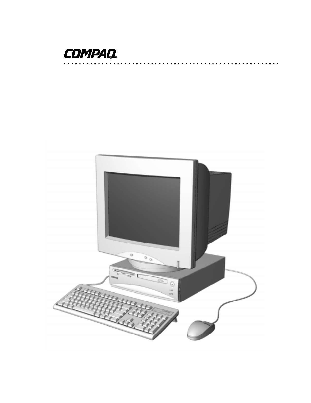
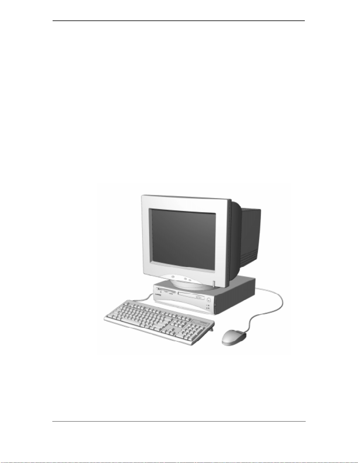
Figure 2–1.
Compaq Deskpro 4000N and 4000S Personal Computers
Compaq Deskpro 4000S Personal Computer with Monitor
First Edition -September
2-1
Page 20

Chapter 2 System Overview
2.2 F EATURES
This section describes the standard and distinguishing features.
2.2.1 STANDARD FEATURES
The following standard features are included on all models:
♦ Pentium micr oprocessor with MMX tech nology
♦ 256-KB second-level cache
♦ 16 or 32 megabytes of SDRAM, with support for ECC and SDP m emory
♦ Integrated S3 Trio64V2/GX graphics controller with 2-MB frame
♦ Enha nced IDE controller support i ng Ultra ATA (UDMA) modes 0-2
♦ Hard drive fault prediction
♦ PCI con nector
♦ Two serial interfaces
♦ Parallel interface
♦ Two universal serial bus ports
♦ Integrated n etwork interface controller (RJ-45/AUI ports)
♦ Compaq Space Saver keyboard w/Windows support
♦ Compaq PS/2-type mouse
♦ APM 1.2 power management suppor t
♦ Plug ’n Play compatible (with ESCD support)
♦ Energy Star compliant
♦ 76-watt, surge-tolerant power supply
The Deskpro 4000N and 4000S support the Intelligent Manageability features listed below:
Configuration
Management
Remote ROM Flash RAM Type Data ECC RAM Fault Prediction Memory Change Alert
Remote Security DMI BIOS SMART II Hard Drive Ownership Tag
Remote Wakeup Asset Tag Monitor Fault Diag. Config. Cntrl. Hardware
Remote Shutdown Sys. Serial # UDMA Integrity Log. Setup Password
Replicated Setup Sys. Manuf./Model Proactive Backup Power-On Password
ACPI-Ready Sys. Board Rev. Level Thermal Sensor QuickLock/QuickBlank
Dual-State Power Sw. ROM rev. Diskette Boot Cntrl.
Failsafe Boot Bloc k ROM Hard Drive Type Data Diskette Write Cntrl.
Asset
Management
Monitor Type Data I/O Port En/Dis. Cntrl.
Compaq Insight Ed itio n Cable Lock Provision
Fault
Management
Security
Management
The Intelligent Manageability features provide support for DMI 2.0, Compaq Insight Manager,
and Management Solutions Partners.
2-2
Compaq Deskpro 4000N and 4000S Personal Computers
Firs t Edition - September 1997
Page 21

2.2.2 MODEL DIFFERENCES
Deskpro 4000N Deskpro 4000S
PCI connector: 1 1 (shared slot)
ISA connector: none 1 (shared slot)
OS installed: Windows NT 4.0 Windows 95
Remot e boot support: Yes No
Diskette drive installed: No Yes
Hard drive size: 1.6 or 2.1 GB 2.1 GB
CD-ROM support: No Yes
2.2.3 OPTIONS
Options that are specific to the Compaq Deskpro 4000N and 4000S Series Personal Computers
include:
♦ System Memory: 8 -MB DIMM
16-MB DIMM
32-MB DIMM
64-MB DIMM
128-MB DIMM
Technical Reference Guide
Compaq Deskpro Computers are easily upgraded and enhanced with peripher a l devices designed
to meet PCI and ISA standards. The Compaq Deskpro Personal Computers are compatible with
peripherals design for Plug ’n Play operation.
Compaq Deskpro 4000N and 4000S Personal Computers
First Edition -September
2-3
Page 22
Chapter 2 System Overview
2.3 MECHANICAL DESIGN
This section illustrates the layout used by the formfactor. In addition, this section includes the
layout of the system board.
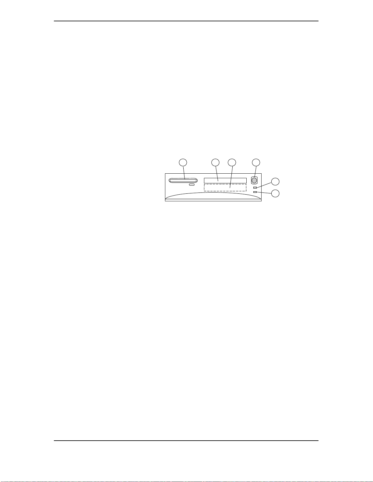
2.3.1 CABINET LAYOUT
NOTES:
[1] Deskpro 4000S only
[2] Front panel access on 4000S only.
Figure 2–2.
Item Function
1 Power Switch
2 Power-On Light
3 Hard Drive Activity Light
4 1.44 MB Diskette Drive (3.5” Drive) [1]
5 1/3 Height Drive Bay (3.5” or 5.25” Drive) [2]
6 1/3 Height Drive Bay (3.5” or 5.25” Drive)
Cabinet Layout, Front View
4 5 6
1
2
3
2-4
Compaq Deskpro 4000N and 4000S Personal Computers
Firs t Edition - September 1997
Page 23
Technical Reference Guide
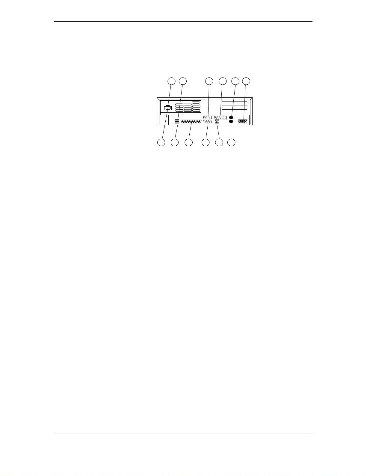
2 4 6 101112
1 3
Item Function
1 AC Line In Connector
2 Line Voltage Select Switch
3 Universal Serial Bus Interface port 1
4 Universal Serial Bus Interface port 2
5 Parallel Interface Connector
6 Serial Interface Connector B
7 Serial Interface Connector A
8 Network Interface AUI Connector
9 Network Interface RJ-45 Connector
10 Mouse Connector
11 Keyboard Connector
12 Monitor Interface
7
8
95
Figure 2–3. Cabinet Layout, Rear View
Compaq Deskpro 4000N and 4000S Personal Computers
2-5
First Edition -September
Page 24
Chapter 2 System Overview
]
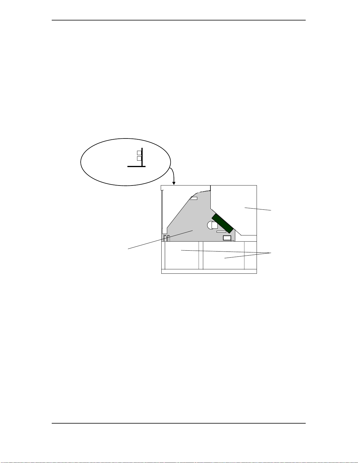
2.3.2 CHASSIS LAYOUT
ISA Combo Slot 1 [1
PCI Combo Slot 1
Slots On Riser Card,
Rear View
Back
System Board
NOTES:
[1] Deskpro 4000S only
Figure 2–4.
Power Supply
Drive Bays
Front
Chassi s La yout, Top Vi ew
2-6
Compaq Deskpro 4000N and 4000S Personal Computers
Firs t Edition - September 1997
Page 25
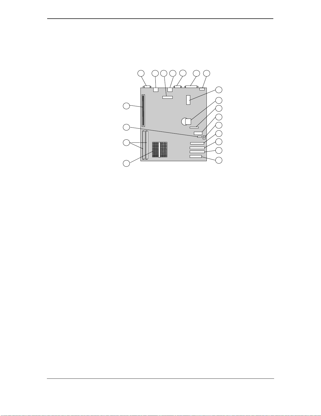
2.3.3 SYSTEM BOARD LAYOUT
1 3
20
19
18
Technical Reference Guide
2
4
6 7
5
8
9
10
11
12
13
14
15
17
16
System Board
p/n 006582-xxx (4000S)
or
p/n 007602-xxx (4000N)
Item Function
1 Graphics monitor connector (J2)
2 Top, Mouse interface connector; Bottom, keyboard connector (J9)
3 NIC AUI connector header (P15)
4 NIC RJ-45 connector (J5)
5 Serial interface connector (P24)
6 Parallel interface connector (J3)
7 Universal serial bus connectors (J6)
8 Power supply connector (P17)
9 RTC/CMOS Battery
10 RTC/CMOS battery replacement header (P14)
11 Power switch, PWR/HD LED cable connector (P16)
12 Processing frequency configuration switch (SW1)
13 CD-ROM connector (P25)
14 Secondary IDE connector (P21)
15 Primary IDE connector (P20)
16 Diskette drive connector (J1)
17 Microprocessor (in type 7 socket)
18 DIMM sockets (J7, J8)
19 CD-ROM drive connector P25 audio out (J11)
20 Riser card connector (J4)
Figure 2–5.
System Board Layout, Component Side
Compaq Deskpro 4000N and 4000S Personal Computers
First Edition -September
2-7
Page 26

Chapter 2 System Overview
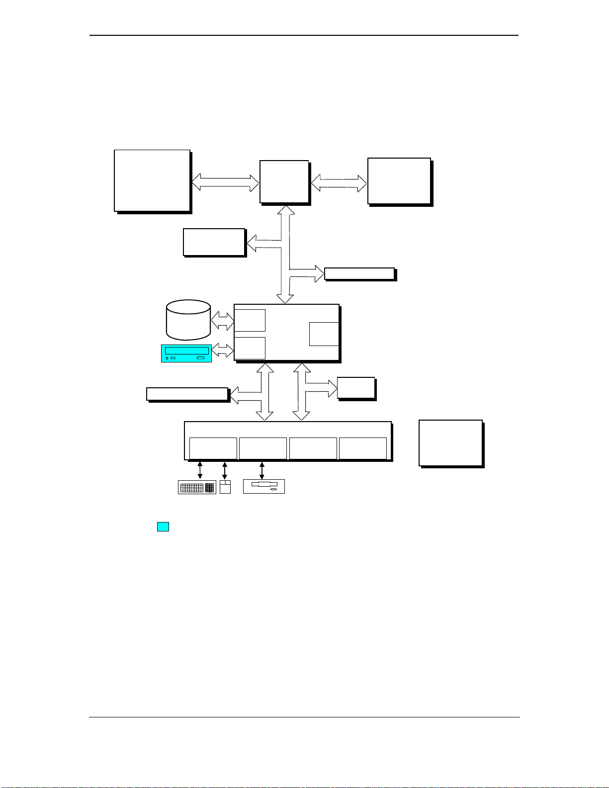
2.4 SYSTEM ARCHITECTURE
The Compaq Deskpro 4000N and 4000S Personal Computers featur ing MMX technology are
based on a Pent i u m MXX micropr ocessor matched with a support chipset that is complimentary
in design. Both th e “N” and “S” systems share the same basic architecture (Figure 2-7), which
utilizes three main buses: the Host bus, the Peripheral Component Interconnect (PCI) bus, and
the Industry Standard Architecture (ISA) bus.
The Host bus provides high performance support for CPU, cache and system memory accesses,
and on these systems is set to operate at 66 MHz. The 32-bit PCI bus provides support for the
graphics subsystem, the EIDE controllers, and expansion devices designed for high performance.
The PCI bus operates at 33 MHz. The ISA bus provides a standard 8-MHz interface for the
input/output (I/O) devices such as the keyboard, diskette drive, serial and parallel interfaces, as
well as the addition of 16- or 8-bit expansion devices.
The CPU/PCI and PCI/ISA bridge functions are handled by the specific support chipset matched
with the microprocessor employed. The support chipset also provides memory controller and data
buffering functions as well as bus control and arbitration functions.
The I/O port functions and diskette dri ve controller ar e in t egra t ed in t o th e PC87307 I/O
Controller. This component also includes the real time clock and battery-backed configuration
memory (CMOS).
Table 2-1 lists the archit ectural highlights.
Table 2–1.
Architectural Comparison
Table 2-1
.
Architectur al Overview
Microprocessor Pentium MMX
Support Chipset VIA VP2
System Memory
Standard installed:
Expandable to:
Cache Memory
L1:
L2:
Graphics Subsystem S3 TrioV2-based
NOTES:
[1] Depending on model
[2] Integrated with the microprocessor
Type
16/32 MB [1]
256 MB
32 KB [2]
256 KB
integrated on board
The following subsections provide a description of the key functions and subsystems.
2-8
Compaq Deskpro 4000N and 4000S Personal Computers
Firs t Edition - September 1997
Page 27
Technical Reference Guide
(2)
]
Microprocessor
and Cache Memory
Hard Drive
CD-ROM
ISA Connector [1
64-Bit Host Bus
Graphics
Subsystem
EIDE
Keyboard/
Mouse I/F
North
Bridge
Pri.
IDE I/F
Sec.
IDE I/F
8-/16-Bit
ISA Bus
PC 87307 I/O Controller
South
Bridge
Diskette
I/F
32-Bit
PCI Bus 0
USB
I/F (2)
X-Bus
Serial
I/F
Mem. Bus
PCI Connector
System
Memory
BIOS
ROM
Parallel
I/F
EIDE
Hard Drive
Power
Supply
NOTES:
CD models only.
[1] Deskpro 4000S only.
Figure 2–6. Compaq Deskpro 4000N and 4000S System Architecture, Block diagram
Compaq Deskpro 4000N and 4000S Personal Computers
First Edition -September
2-9
Page 28

Chapter 2 System Overview
2.4.1 MICROPROCESSOR
The Compaq Deskpro 4000N and 4000S Personal Computers feature the Pentium MMX
microprocessor that is backward-compatible with software written for x86-type processors. The
Pentium MMX microprocessor inclu des a 3 2 KB L1 cache and ext ensions t o the inst ruction set
that pr ovide higher per forman ce for processing graphics and video code. The microprocessor is
mounted in a ZIF type-7 socket that allows replacing and/or upgrading.
Pentium MMX Microprocessor
Figure 2–7.
2.4.2 MEMORY
This system includes 256 kilobytes of SRAM for secondary (L2) cache support of the
microprocessor’s primary (L1) cache. The L2 cache is arranged as direct-mapped, write-through
using synchronous pi p elined bur st SRAMs.
For system memory two 168-pin DIMM sockets are provided with 16 or 32 megabytes of unbuffered SDRAM installed depending on model. System memory can be expanded up to 256
megabytes using 8-, 16-, 32-,64-, and 128-MB DIMMs. Both EDO and SDRAM DIMMs are
supported (SDRAM DIMMs are recommended). T he system supports the use of ECC memory as
well.
Dual-ALU
CPU w/MMX
Branch
Prediction
(Mounted in Type 7 Connector)
32-KB
Cache
Dual Pipeline
Math Coproc.
Micr oprocessor A rchitectu ral Diag ram
The system ROM utilizes a flash ROM component that contains the BIOS and stores PCI, ESCD,
and EV data. The BIOS is updateable by remote or local flashing of the ROM, which includes
boot bloc k ROM support .
2-10
Compaq Deskpro 4000N and 4000S Personal Computers
Firs t Edition - September 1997
Page 29

2.4.3 SUPPORT CHIPSET
Table 2-2 shows the chipsets used for the Deskpro 4000N and 4000S systems.
Technical Reference Guide
Table 2–2.
Function Component
Host/PCI (North) Bridge:
System Controller
Data Buffer
PCI/ISA (South) Bridge:
EIDE Controller
DMA Controller
Interrupt Controller
Timer/Counter
NMI Registers
Reset Control Reg.
USB I/F
I/O Controller:
Keyboard I/F
Diskette I/F
Serial I/F
Parallel I/F
RTC/CMOS Mem.
GPIO Ports
Support Chipsets
2.4.4 MASS STORAGE
Table 2-2.
Support Chipsets
VT82C595
“
“
VT82C586
“
“
“
“
“
“
“
87307
“
“
“
“
“
“
A 1.6- or 2.1-GB EIDE hard drive may be installed, depending on series/model. All models
include a PCI bus mastering Enhanced IDE (EIDE) controller that provides two EIDE interfaces
supporting two IDE devices. Master/slave drive selection is determin ed usin g t he cable-select
method, eliminating the need to move jumpers when re-configuring drives. The mass storage
drive bay capacity is determined by the form factor (refer to Section 2.3, Mechanical Design). All
Deskpro 4000S models include a 3.5 inch 1.44-MB diskette drive installed.
2.4.5 SERIAL AND PARALLEL INTERFACES
All models include two serial and one parallel port available at the rear of the unit chassis. The
serial and parallel ports are integrated into a PC87307 I/O Controller component. The serial
ports use 16550/16450-equivalent logic and are RS-232-C compatible and operate at baud rates
up to 115,200. The parallel interface is Enhanced Parallel Port (EPP1.9) and Enhanced
Capability Port (ECP) compatible, and supports bi-directional data transfers.
Compaq Deskpro 4000N and 4000S Personal Computers
First Edition -September
2-11
Page 30

Chapter 2 System Overview
2.4.6 UNIVERSAL SERIAL BUS INTERFACE
Two Universal Serial Bus (USB) ports are included, each providing a high speed interface for
future systems and/or peripherals. The USB interface operates at 12 Mbps and provides hot
plugging/unplugging (Plug ’n Play) functionality.
2.4.7 GRAPHICS SUBSYSTEM
The graphics subsystem is integrated on the system board and operates off the PCI bus. The
subsystem is based on the S3 Trio64 V2/GX controller and includes two megabytes of SGRAM.
The subsystem provides a maximum resolution of 1280 x 1024 with 256 colors.
NOTE:
Table 2–3.
The graph i cs subsystem is not upgradeable.
Graphics Subsystem Overview
Table 2-3.
Graphics Subsystem Overview
Parameter Type
Graphics Controller S3 Trio64V2
Graphics Memory 2 MB SGRAM
Maximum Resolution 1280x1024 @ 256 colors
2-12
Compaq Deskpro 4000N and 4000S Personal Computers
Firs t Edition - September 1997
Page 31

2.5 SPECIFICATIONS
This section includes the environmental, electrical, and physical specifications for the Compaq
Deskpro 4000N and 4000S Series Personal Computers.
Technical Reference Guide
Table 2–4.
Environmental Specifications
Table 2-4.
Environmental Specifications
Parameter Operating Nonoperating
Air Temperature 50
Shock N/A 60.0 g for 2 ms half-sine pulse
Vibration 0.000215g^ 2/Hz, 10-300 Hz [1] 0.0005g^ 2/Hz, 10-500 Hz [1]
Humidity 80% RH @ 36
Maximum Altitude 10,000 ft (3048 m) 30,000 ft (9,144 m)
NOTE:
Table 2–5.
Values are subject to change without notice.
[1] 0.5 grms nominal.
Electrical Specifications
o
to 95o F (10o to 35o C) -24o to 140o F (-30o to 60o C)
o
C (no hard drive) 95% RH @ 36o C
Table 2-5.
Electrical Specifications
Parameter Domestic International
Input Line Voltage:
Nominal:
Maximum:
Input Line Frequency Range:
Nominal:
Maximum:
Power Supply
Maximum Continuous Power:
Maximum Line Current Draw:
100 - 120 VAC
90 - 132 VAC
50 - 60 Hz
47 - 63 Hz
75 watts
5.5 A
200 - 240 VAC
180 - 264 VAC
50 - 60 Hz
47 - 63 Hz
75 watts
?? watts
3.0 A
Table 2–6.
Physical Specifications
Table 2-6.
Physical Specific ations
Dimension Measurement
Height 3.56 in (9.00 cm)
Width 112.50 in (31.80 cm)
Depth 14.60 in (37.10 cm)
Weight 20 lb (9.08 kg)
NOTE:
Metric measurements shown in parenthesis.
Compaq Deskpro 4000N and 4000S Personal Computers
First Edition -September
2-13
Page 32

Chapter 2 System Overview
Table 2–7. Diskette Drive Specifications
Paramemter Measurement
Media Type 3.5 in 1.44 MB/720 KB diskette
Height 1/3
Bytes per Sector 512
Secto rs per T rack:
High Density
Low Density
Tracks p er Side:
High Density
Low Density
Read/Write Heads 2
Average Access Time:
Track-to-Track (high/low)
Average (high/low)
Settling Time
Latency Average
Table 2-7.
Diskette Drive S pec ifications
18
9
80
80
3 ms/3 ms
94 ms/94ms
15 ms
100 ms
Table 2–8. 8x CD-ROM Drive Specifications
Table 2-8.
20x CD-ROM Drive Spec ifications
Paramemter Measurement
Media Type Mode 1,2, Mixed Mode, CD-DA,
Center Hole Diameter 15 mm
Disc Diameter 8/12 cm
Disc Thickness 1.2 mm
Track Pitch 1.6 um
Laser
Beam Divergence
Output Power
Typr
Wave Length
Average Access Time:
Random
Full Stroke
Audio Output Level 0.7 Vrms
Cache Buffer 128 KB (min)
Data Transfer Time
Sustained
Startup Time
Photo CD, Cdi , CD-XA
53.5 +/- 1.5
53.6 0.14 mW
790 +/- 25 nm
150 ms
600 ms
3000 KB/s
7 secs (nom)
°
GaAs
2-14
Compaq Deskpro 4000N and 4000S Personal Computers
Firs t Edition - September 1997
Page 33

Technical Reference Guide
Table 2–9. Hard Drive Specifications
Table 2-9.
Hard Drive Specifications
Parameter 1.6 GB 2.1 GB
Interface: EIDE EIDE
Drive Type: 65 65
Drive Size: 5.25 in 5.25 in
Transfer Rate
Heads:
Interface:
Seek Time (w/settling)
Single Track:
Average:
Full Stroke:
Disk RPM: 4500 4500
EDMA Support: Mode 2 Mode 2
PIO Support: Mode 4 Mode 4
Power Mode Command Support: Yes Yes
Drive Fault Prediction: SMART II SMART II
94.0 Mb/s
16.7 MB/s
2.0 ms
11.0 ms
25.0 ms
27.2-55 Mb/s
16.7 MB/s
2.0 ms
12.0 ms
22.0 ms
Compaq Deskpro 4000N and 4000S Personal Computers
First Edition -September
2-15
Page 34

Chapter 2 System Overview
This page is intentionally blank.
2-16
Compaq Deskpro 4000N and 4000S Personal Computers
Firs t Edition - September 1997
Page 35

Chapter 3
PROCESSOR/
MEMORY SUBSYSTEM
Technical Reference Guide
3.
3.1
Chapter 3 PROCESSOR/MEMORY SUB S YSTEM
INTRODUCTION
This chapter describes the processor/cache memory subsystem of the Compaq Deskpro 4000N
and 4000S Series of Personal Computers.
This chapter includes the following topics:
♦ Pentium MMX-based processor/m em or y subsystem [3.2] page 3-2
♦ Klamath-based processor/memory subsystem [3.4] page 3-12
Table 3-1 lists the highl i ghts of the processor/memory architecture.
Table 3–1.
Processor/Memory Architectural Highlights
Table 3-1.
Processor/Memory
Architectur al Highlights
Feature Type/Amount
Support Chipset VT82C595
System Memory
Standard installed:
Expandable to:
Cache Memory
L1:
L2:
NOTES:
[1] Integrated into the microprocessor
16 or 32 MB SDRAM
256 MB
32 KB [1]
256 KB
Compaq Deskpro 4000N and 4000S Personal Computers
Firs t Edition - September 1997
3-1
Page 36
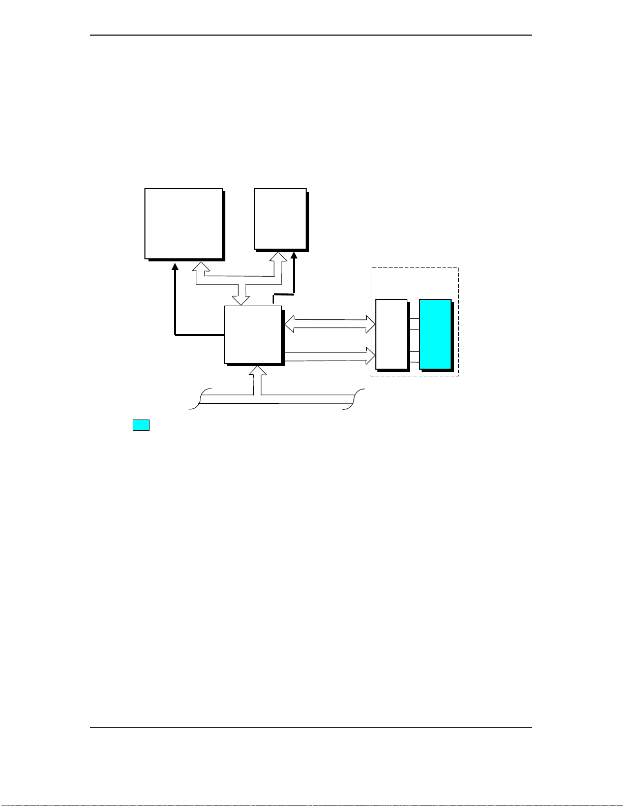
Chapter 3 Processor/Memory Subsystem
()
3.2 PENTIUM MMX-BASED PROCESSO R/M EMORY SUBSYSTEM
The processor/memory subsystem is based on th e Pent i u m MMX m i cr opr ocessor, a 512-KB or 1MB secondary cache, and a VT82C595 system controller (Figure 3-1).
Memory/PCI
Data Buffer
System Memory
J7
16-MB
DIMM
J8
DIMM
Pentium MMX
Microprocessor
Cntl
Optional module
Figure 3–1.
256-KB
Secondary
Cache
64-Bit Host Bus
Cache/
Memory/PCI
Controller
(VT82C595)
Cntl
Mem.
Data Bus
Mem. Addr.
32-bit PCI Bus
Processor/Memory Subsystem Archi t ectu re
The microprocessor is mounted in a ZIF type 7 socket that facilitates easy changing/upgrading.
The system supports both 2.8V and 3.3V core processors. Replacing the microprocessor may
requ ire reconfig u ring a D I P s witch to select t he correct bus frequency/core fr eq u ency
combination. Frequency selection is described in detail later in this section.
The VT82C595 system controller pr ovides the Host/PCI bridge functions and contr ols tr a nsfers
with the 64-bit memory data bus. The system includes 256 kilobytes of SRAM controlled by the
system controller as a direct-mapped, write-through L2 cache to the L1 cache integrated into the
microprocessor. Th e system supports synchronous, pipelin ed burst SRAM/DRAM for the L2
cache, providing 3-1-1-1 read/write cycles at 60 and 66 MHz on a cache hit .
The standard system memory configuration consists of 16 or 32 megabytes of SDRAM system
memory. The system memory can be expanded to 256 megabytes.
Compaq Deskpro 4000N and 4000S Personal Computers
3-2
Firs t Edition - September 1997
Page 37
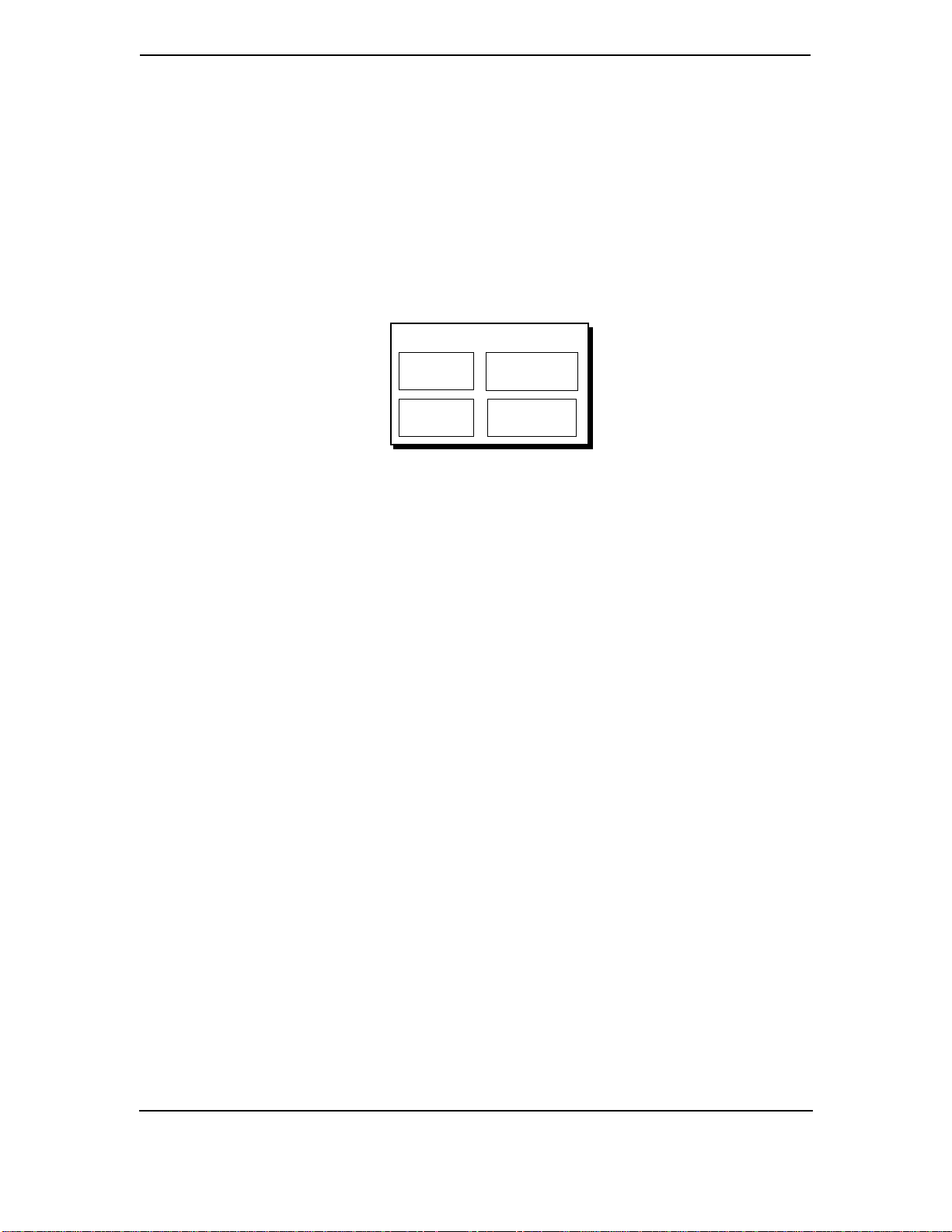
3.2.1 PENTIUM MMX MICROPROCESSOR
The Pentium MMX microprocessor is softwar e-compatible with earlier generation x86
microprocessors but provides significantly higher performance due to both higher processing
speed and enhanced design (Figure 3-2.).
Pentium MMX Microprocessor
Technical Reference Guide
Figure 3–2.
Pentium MMX Micropr ocessor Internal Architect ure
The Pentium MMX microprocessor contains a dual-ALU CPU, branch prediction logic, dualpipeline math coprocessor, and a 32-KB cache that is split into two 16-KB 4-way, set-associative
caches for handling code and data separately. The microprocessor is mounted in a ZIF type 7
socket for easy changing/upgrading of the microprocessor. Replacing the micr oprocessor may
require reconfiguring the settings of DIP switch SW1 to properly set the speed of the Host bus
and the core (processing) frequencies.
3.2.1.1 MMX Technology
The CPU of the Pentium MMX support s 57 a dditional instructions specifically designed for
accelerating multimedia and communications applications. Such applications often involve
compute-intensive loops that can take up as much as 90 percent of CPU execution time. The
MMX logic, using a pa rallel processing technique called Single Instruction-Multiple Data
(SIMD), operates on 64 bits at a time. The MMX instructi on s a re design ed t o take advan t a g e of
the dual-pipeline CPU as well as help the programmer in avoiding branches in code. Specific
applications that benefit from MMX technology in clude 2D/ 3 D g raphics, audio, sp eech
recognition, video codecs, and data compression .
CPU
w/MMX
Branch
Prediction
32-KB
Cache
Dual Pipeline
Math Coproc.
NOTE:
MMX operations utilize a portion of the floating point registers of the
integrated math coprocessor. Programmers should take note that mixing MMX code
with that of floating point operations can result in reduced performance and should
there fore be avoid e d.
.
Compaq Deskpro 4000N and 4000S Personal Computers
Firs t Edition - September 1997
3-3
Page 38

Chapter 3 Processor/Memory Subsystem
3.2.2 BU S/ PRO CES S ING S PEED SELECT
The Pentium MMX-based system board i ncludes a four- p osition DIP switch (SW1) that is used to
select the Host bus frequency and the processing frequency of the system. The SW1 positions 2
and 3 control the Bus Fraction (BF0, BF1) signals to the CPU, which determines the bus-to-core
speed ratio. Position 5 of SW1 determines the bus frequency generated by the clock generator
(refer to Chapter 4, “System Support” for more information on clock frequency generation).
Table 3-2 shows the switch configurations to be used with a particular microprocessor.
Table 3–2.
Pentium MMX Micropr ocessor Bus/Core Speed Switch Settings
Table 3-2.
Pentium MMX Microprocessor
Bus/Core Speed Swit c h ( S W1) Settings
DIP SW1 Settings [1]
235
Off Off Off 60/210
Off Off On 66/233
Off On Off 60/180
Off On On 66/200
On Off Off 60/120
On Off On 66/133
On On Off 60/150
On On On 66/166
NOTES:
Shipping configurations are unshaded
Microprocessor
Bus/Core Spee d (in MHz)
NOTE:
SW1 should be set to match
the specified core speed of the
microprocessor. Configuring
for a core speed lower or
higher than that for which the
CPU is designed can result in
unstable or possibly
destructive operation.
The status of SW1-2, -3, and -5 is readable through general-purpose I/O (GPIO) port 78h bits
<2..0>, allowing BIOS and/or diagnostic software to check an installed microprocessor with the
switch configuration. Table 3-3 shows the switch position-to-GPIO-to-I/O port 78h input wiring.
Table 3–3
. SW1 Bus/Core Speed Positions to GPIO Assignments
Table 3-3.
SW1 Bus/Core S peed P os itions
to GPIO A s s ignm ents
Switch Position Signal Name GPIO Number I/O Port 78h
SW1-2 BF0 10 bit <0>
SW1-3 BF1 11 bit <1>
SW1-5 SPD66- 12 bit <2>
SPD = Bus frequency select BF = Bus/core fraction
3.2.3 SECONDARY (L2) CACHE MEMO RY
The system board comes with 256 kilobytes of SRAM implemented as the secondary (L2) cache
to the integrated L1 cache of th e Pen tium MMX microprocessor. This L2 cache uses two 32K x
32 synchronous pipelined burst SRAMs (with one 32K x 8 T AG RAM) a rra nged as a directmapped, write-back. The L2 cache provides a typical cycle time (in Host clocks) of 3-1-1-1 for
burst reads (cache hit) and writes (write back). The L2 controller allows the full system memory
range t o be cached.
Compaq Deskpro 4000N and 4000S Personal Computers
3-4
Firs t Edition - September 1997
Page 39

3.2.4 SYSTEM MEMORY
The system board contains two 168-pin DIMM sockets for system memory. This system is
designed for u si ng SDRAM DIMMs. As sh i p p ed fr om t he factory the sta ndard configur ation may
be 16 or 32 megabytes installed. The addition of 16-, or 32-, 64-, or 128-MB DIMMs allows the
expansion of system memory up to a maximum of 256 megabytes. Single or double-sided
DIMMs may be used. It is strongly recommended to use DIMMs with gold-plated contacts.
The system memory uses the following RAS line assignments:
RAS#0 DIMM 1, Ban k A
RAS#1 DIMM 1, Ban k B
RAS#2 DIMM 2, Ban k A
RAS#3 DIMM 2, Ban k B
This system does not use parity but does support ECC, and the memory is unbuffered. The
performance times of the SDRAM is listed as follows:
Technical Reference Guide
Table 3–4.
SDRAM Performance Times
Table 3-4.
SDRAM Performance Times
Parameter CAS Latency = 2 CLKs
Burst Read Page Hit: 6-1-1Read Row Miss 8-1-1-1
Read Page Miss 10-1-1-1
Bk-to-Bk Burst Reads (Pg Hit ) 6-1-1-1, 3-1-1-1
Write Page Hit 3
Write Row Miss 6
Write Page Miss 9
Posted Write 3-1-1-1
In addition to the supplied (and recommended) SDRAM, the system supports EDO and ECC
RAM, with error logging/alerting supported. The RAM type (as well as other information) is
detected during power-up by the system BIOS using the serial presence detect (SPD) meth od,
which reads the EEPROM on each DIMM to obtain identification data such as the type and
operating parameters. The supported format complies to the JEDEC specification for 128-byte
EEPROMs. Thi s system also provides support for 256-byte EEPROMs to include additional
Compaq-added features such as the part number, serial number, and error logging. The SPD
format as supported in this system is shown in Table 3-5.
Compaq Deskpro 4000N and 4000S Personal Computers
Firs t Edition - September 1997
3-5
Page 40

Chapter 3 Processor/Memory Subsystem
Table 3–5. SPD Addr ess Map ( SDRAM DIMM)
SPD Address Map (SDRAM DIMM)
Byte Description Notes Byte Description Notes
0 No. of Bytes Written Into EEPROM [1] 62 SPD Revision [7]
1 Total Bytes (#) In EEPROM [2] 63 Checksum Bytes 0-62
2 Memory Type 64-71 JEP-106E ID Code [8]
3 No. of Row Addresses On DIMM [3] 72 DIMM OEM Location [8]
4 No. of Column Addresses On DIMM 73-90 OEM’s Part Number [8]
5 No. of Module Banks On DIMM 91, 92 OEM’s Rev. Code [8]
6, 7 Data Width of Module 93, 94 Manufacture Date [8]
8 Voltage Interface Standard of DIMM 95-98 OEM’s Assembly S/N [8]
9 Cycletime @ Max CAS Latency (CL) [4] 99-125 OEM Specific Data [8]
10 Access From Clock [4] 126, 127 Reserved
11 Config. Type (Parity, Nonparity, etc.) 128-135 Sys. Integrator’s ID [9]
12 Refresh Rate/Type [4] [5] 136-150 Sys. Integrator’s P/N [9]
13 Width, Primary DRAM 151-152 Sys. Integrator’s D/C [9]
14 Error Checking Data Width 153-165 Sys. Integrator’s S/N [9]
15 Min. Clock Delay [6] 166 Chksm Bytes 128-165 [9]
16 Burst Lengths Supported 167-189 Top Level Sys. S/N [9]
17 No. of Banks For Each Mem. Device [4] 190-221 Avaiable for use [9]
18 CAS Latencies Supported [4] 222 Chksm Bytes 167-221 [9]
19 CS# Latency [4] 223-253 Available for use [9]
20 Write Latency [4] 254 Chksm Bytes 223-253 [9]
21 DIMM Attributes 255 Chksm Byes 0-128 [9]
22 Memory Device Attributes
23 Min. Clock Cycle Time at CL X-1 [7]
24 Max. Acc. Time From CLK at CL X-1 [7]
25 Min. Clock Cycle Time at CL X-2 [7]
26 Max. Acc. Time From CLK at CL X-2 [7]
27 Min. Row Precharge Time [7]
28 Min. Row Active To Row Active Delay [7]
29 Min. RAS to CAS Delay [7]
30, 31 Reserved
32..61 Superset Data For Future Use
NOTES:
[1] Programmed as 128 bytes by the DIMM’s OEM
[2] Must be programmed to 256 bytes.
[3] High order bit defines redundant addressing: if set (1), highest order RAS# address must be
re-sent as highest order CAS# address.
[4] Refer to memory manufacturer’s datasheet
[5] MSb is Self Refresh flag. If set (1), assembly supports self refresh.
[6] Back-to-back random column addresses.
[7] Field format proposed to JEDEC but not defined as standard at publication time.
[8] Field specified as optional by JEDEC but required by this system.
[9] Field format proposed to JEDEC. This system requires that the DIMM’s EEPROM have this
space available for reads/writes.
Table 3-5.
Access to the DIMM’s EE PROM is t hrough an I2C-type bus interface using BIOS call INT 15,
AX-E827h (discussed in Chapter 8, “BIOS ROM”).
If the BIOS finds an installed module that is not supported then the memory controller is
programmed to indicate empty rows as appropriate.
Compaq Deskpro 4000N and 4000S Personal Computers
3-6
Firs t Edition - September 1997
Page 41

Figure 3-3 shows the system memory map.
(
)
(
)
Technical Reference Guide
Host,
PCI Area
Host, PCI,
ISA Area
DOS Compatibility
Area
FFFF FFFFh
FFFC 0000h
FFFB FFFFh
8100 0000h
80FF FFFFh
8000 0000h
7FFF FFFFh
1000 0000h
FFDF FFFFh
1000 0000h
0FFF FFFFh
0400 0000h
03FF FFFFh
0100 0000h
00FF FFFFh
0010 0000h
000F FFFFh
000F 0000h
000E FFFFh
000E 0000h
000D FFFFh
000C 8000h
000C 6800h
000C 6000h
000C 5FFFh
000C 0000h
000B FFFFh
000A 0000h
0009 FFFFh
High BIOS Area
256 KB
PCI Memory
(2130 MB)
ISA Memory-Mapped
Device s (16 MB)
PCI Memory
(1792 MB)
Op.TSEG (Cacheable)
(.1, .25, .5, 1 MB)
Op. Hi SMRAM
(384 KB)
Cacheable in L1
(192 MB)
Extended Memory
(48 MB)
Extended Memory
15 MB
Upper BIOS Area
(64 KB)
Lower BIOS Area
(64 KB)
Unused 96 KB
Graphics ROM
(6 KB)
Unused 2 KB
Graphics ROM
(24 KB)
Graphics/SMM Area
(128 KB)
4 GB
64 MB
16 MB
1 MB
960 KB
896 KB
800 KB
792 KB
768 KB
640 KB
Base Memory
(640 KB)
0000 0000h
NOTE: All locations in the 256 megabytes of system memory are cacheable in the L2 cache.
Figure 3–3. System Memory Map
Compaq Deskpro 4000N and 4000S Personal Computers
Firs t Edition - September 1997
3-7
Page 42

Chapter 3 Processor/Memory Subsystem
3.2.5 SUB S YSTEM CONFIGURATION
The VT82C595 component provides the configuration function for the processor/memory
subsystem. Table 3-6 lists the configuration registers used for setting and checking such
parameters as cache (L2) control, system memory control, and PCI bus operation. These registers
reside in the PCI Configuration Space and accessed using the methods described in Chapter 4,
section 4.2.
Table 3–6.
Host/PCI Bridge Configuration Registers (VT82C595)
Table 3-6.
Host/PCI B r idge Configuration Registers ( V T82C595)
PCI Config.
Addr. Register
00, 01h Vender ID 1106h 64h DRAM Timing ABh
02, 03h Device ID 0595h 65h DRAM Control Reg. 1 00h
04, 05h Command 0007h 66h DRAM Control Reg. 2 00h
06, 07h Status 67h DRAM Width 00h
08h Revision ID 68h UMA Control Reg. 1 00h
09-0Bh Class Code 69h UMA Control Reg. 2 00h
0Dh Latency Timer 00h 6Ah Refresh Control 00h
0Eh Header Type 00h 6Bh Misc. Cointrol 00h
0Fh BIST (read only) 6Ch SDRAM Control
50h Cache Control Reg. 1 00h 6Dh DRAM Control Drive Strength
51h Cache Control Reg. 2 00h 6Eh ECC Control Reg.
52h Non-Cacheable Control 02h 6Fh ECC Status Reg.
53h Misc. Control 00h 70h PCI Buffer Control 00h
54, 55h Non-Cacheable Area 1 00h 71h CPU-to-PCI Flow Cntl. Reg. 1 00h
56, 57h Non-Cacheable Area 2 00h 72h CPU-to-PCI Flow Cntl. Reg. 2 00h
58h DRAM Configuration 40h 73h PCI Master Control Reg.1 00h
59h DRAM Configuration 05h 74h PCI Master Control Reg. 2 00h
5A..5Fh DRAM ROW End Addr. 01h 75h PCI Arbitration 00h
60h DRAM Type 00h 76h Extension (PCI Arbitration) 00h
61..63h Shadow RAM Control 00h -- -- --
NOTE:
Refer to VIA Technologies, Inc. documentation for detailed description of registers.
Assume unmarked locations/gaps as reserved.
Reset
Value
PCI Config.
Addr. Register
Reset
Value
Compaq Deskpro 4000N and 4000S Personal Computers
3-8
Firs t Edition - September 1997
Page 43

Chapter 4
SYSTEM SUPPORT
4. Chapter 4 SYSTEM SUPPORT
Technical Reference Guide
4.1
INTRODUCTION
This chapter covers subjects dealing with basic system architecture and covers the following
topics:
♦ PCI bus overview (4.2) page 4-2
♦ ISA bus overview (4.3) pa ge 4-11
♦ System clock distribution (4.4) page 4-23
♦ Real-time clock and configuration memory (4.5)page 4-24
♦ I/O map and r egister accessing (4.6) page 4-41
♦ System management support (4.7) page 4-44
This chapter covers functions provided by off-the-shelf chipsets and therefore describes only basic
aspects of these functions as well as information unique to the Compaq Deskpro 4000 Personal
Computers. For detailed information on specific components, refer to the applicable
manufacturer’s documentation.
Compaq Deskpro 4000N and 4000S Personal Computers
Firs t Edition - September1997
4-1
Page 44

Chapter 4 System Support
4.2 PCI BUS OVERVIEW
NOTE:
This section describes the PCI bus in general and highlights bus
implementation in this particular system. For detailed information regarding PCI bus
operation, refer to the PCI Local Bus Specification Revision 2.1.
This system implements a 32-bit Peripheral Component In t er conn ect (PCI) bus. The PCI bus
uses a shared address/data bus design. On the first clock cycle of a PCI bus transaction the bus
carries address information. On subsequent cycles, the bus carries data. PCI transactions occur
synchronously with the Host bus at a rate of up to 33 MHz, depending on the speed of the
microprocessor used. All I/O transactions involve the PCI bus. All ISA transactions involving the
microprocessor, cache, and memory also involve the PCI bus. Memory cycles will involve the
PCI if the access is initiated by a device or subsystem other than the microprocessor.
The PCI bus handles address/data transfers through the identification of devices and functions on
the bus (Figure 4-1). A device is defined as a component or slot that resides on the PCI bus. A
function is defined as the end source or target of the bus transaction. A device (component or
slot) may contain one or more functions (i.e., in this system the PCI/ISA Bridge function, EIDE
controller function, USB function, and ACPI function are contained within the South Bridge
component).
Host Bus
Host/PCI
Bridge Function
32-Bit PCI Bus 0
PCI/ISA Bridge
Function
Figure 4–1.
Compaq Deskpro 4000N and 4000S Personal Computers
4-2
PCI Bus Devices and Functions
EIDE Cntlr.
Function
ISA Bus
Graphics
Controller
USB
Function
ACPI Cntlr.
Function
PCI Connector
NIC
Function
Firs t Edition - September 1997
Page 45

4.2.1 PCI CONNECTOR
Technical Reference Guide
B94
A94
B1B62
A62
NOTE: See caution below.
Figure 4–2.
Table 4–1.
32-Bit PCI Bus Connector (32-Bit Type)
32-Bit PCI Bus Connector Pinout
A1
Table 4-1.
PCI Bus Connector P inout
Pin B Signal A Signal Pin B Signal A Signal Pin B Signal A Signal
01 -12 VDC TRST- 32 AD17 AD16 63 Reserved GND
02 TCK +12 VDC 33 C/BE2- +3.3 VDC 64 GND C/BE7-
03 GND TMS 34 GND FRAME- 65 C/BE6- C/BE5-
04 TDO TDI 35 IRDY- GND 66 C/BE4- +5 VDC
05 +5 VDC +5 VDC 36 +3.3 VDC TRDY- 67 GND PAR64
06 +5 VDC INTA- 37 DEVSEL- GND 68 AD63 AD62
07 INTB- INTC- 38 GND STOP- 69 AD61 GND
08 INTD- +5 VDC 39 LOCK- +3.3 VDC 70 +5 VDC AD60
09 PRSNT1- Reserved 40 PERR- SDONE 71 AD59 AD58
10 RSVD +5 VDC 41 +3.3 VDC SBO- 72 AD57 GND
11 PRSNT2- Reserved 42 SERR- GND 73 GND AD56
12 GND GND 43 +3.3 VDC PAR 74 AD55 AD54
13 GND GND 44 C/BE1- AD15 75 AD53 +5 VDC
14 RSVD Reserved 45 AD14 +3.3 VDC 76 GND AD52
15 GND RST- 46 GND AD13 77 AD51 AD50
16 CLK +5 VDC 47 AD12 AD11 78 AD49 GND
17 GND GNT- 48 AD10 GND 79 +5 VDC AD48
18 REQ- GND 49 GND AD09 80 AD47 AD46
19 +5 VDC Reserved 50 Key Key 81 AD45 GND
20 AD31 AD30 51 Key Key 82 GND AD44
21 AD29 +3.3 VDC 52 AD08 C/BE0- 83 AD43 AD42
22 GND AD28 53 AD07 +3.3 VDC 84 AD41 +5 VDC
23 AD27 AD26 54 +3.3 VDC AD06 85 GND AD40
24 AD25 GND 55 AD05 AD04 86 AD39 AD38
25 +3.3 VDC AD24 56 AD03 GND 87 AD37 GND
26 C/BE3- IDSEL 57 GND AD02 88 +5 VDC AD36
27 AD23 +3.3 VDC 58 AD01 AD00 89 AD35 AD34
28 GND AD22 59 +5 VDC +5 VDC 90 AD33 GND
29 AD21 AD20 60 ACK64- [1] REQ64- [1] 91 GND AD32
30 AD19 GND 61 +5 VDC +5 VDC 92 Reserved Reserved
31 +3.3 VDC AD18 62 +5 VDC +5 VDC 93 Reserved GND
-- -- -- -- -- -- 94 GND Reserved
NOTE:
[1] The REQ64- and ACK64- signals are pulled high, allowing the use of 64-bit PCI cards
in 32-bit mode.
CAUTION:
The maximum length for an expansion card (PCI or ISA) installed in this system is
7 inches. Longer cards may be damaged or cause damage to the system.
Compaq Deskpro 4000N and 4000S Personal Computers
Firs t Edition - September1997
4-3
Page 46

Chapter 4 System Support
4.2.2 PCI BUS MASTER ARBITRATION
The PCI bus supports a bus master/target arbitration scheme. A bus master is a device that has
been granted control of the bus for the purpose of initiating a transaction. A target is a device that
is the recipient of a transaction. Request (REQ), Grant (GNT), and FRAME signals are used by
PCI bus masters for gaining access to the PCI bus. When a PCI device needs access to the PCI
bus (and does not already own it), the PCI device asserts it’s REQn signal to the PCI bus arbiter
(a function of the system controller component). If the bus is available, the arbiter asserts the
GNTn signal to the requesting device, which then asserts FRAME and conducts the address
phase of the transaction with a target. If the PCI device already owns the bus, a request is not
needed and the device can simply assert FRAME and conduct the tra nsaction. Table 4-1 shows
the grant and request signals assignments for the devices on the PCI bus.
Table 4–2.
PCI Bus Mastering Devices
Table 4-2.
PCI Bus Mast er ing Dev ic es
REQ/GNT Line Device
REQ1/GNT1 PCI Connector
REQ2/GNT2 Graphics Controller
REQ3/GNT3 Network I/F Controller
PCI bus contr ol is gr ant ed according to a Least Recently Used (LRU) algorithm. D u ring times
that the bus is not used or requested, bus control is given to the Host/PCI bridge. After a device
has g iven up control of the bu s or ha s not execu ted a t ransact i on for 16 P C I clock cycles
(PCICLKs) after gaining bus control, it loses access and is placed on the bottom of the priority
list.
The PCI/ISA bridge is given special consideration. If the PCI/ISA bridge gains control of the PCI
bus but does not execute a transaction after 16 PCICLKs, the PCI/ISA bridge retains ownership
of the PCI bus until the current ISA bus master relinquishes the ISA bus. The PCI/ISA bridge is
then placed on the bottom of the priority list.
PCI bus priority can be altered in two ways: by a master needing to perform a retry of a data
cycle, or by the master locking the bus. When a master is retried, it releases the bus and negates
its REQn- line for a minimum of two PCICLKs and th en requests the bus again. If the master is
granted the bus before the condition that caused the retry is resolved, the master is retried again,
which may result in bus “thrashing.” Bus thrashing is minimized by masking the REQn- line of a
particular device that has had a transaction retried.
If a master locks the PCI bus, it retains top priority, allowing it to quickly finish a lock sequence.
The PCI/ISA bridge cannot become master until the locking device unlocks the bus.
Consequently, a master should not lock the bus for long periods of time or latency problems could
occur.
Compaq Deskpro 4000N and 4000S Personal Computers
4-4
Firs t Edition - September 1997
Page 47

4.2.3 PCI BUS TRANSACTIONS
The PCI bus consists of a 32-bit path (AD31-00 lines) that uses a multiplexed scheme for
handling both address and data transfers. A bus transaction consists of an address cycle and one
or more data cycles, with each cycle requiring a clock (PCICLK) cycle. High performance is
realized during burst modes in which a transaction with contiguous memory locations requires
that only one address cycle be conducted and subsequent data cycles are completed using autoincremented addr es s i ng. F our types of address cycles can t ake place on the PCI bus ; I/O,
memory, configuration, and special. Address decoding is distributed (left up to each device on
the PCI bus).
4.2.3.1 I/O and Memory Cycles
For I/O and memory cycles, a standard 32-bit addr ess decode (AD31..0) for byte-level addressing
is handled by the appropriate PCI device. For memory addressing, PCI devices decode the
AD31. .2 li nes for d wor d -level a d d ressi ng and check the AD1, 0 lin es for burst (li nearincrementing) mode. In burst mode, subsequent data phases are conducted a dword at a time with
addressing assumed to increment accordingly (four bytes at a time).
Technical Reference Guide
4.2.3.2 Configuration Cycles
Devices on the PCI bus must comply with PCI protocol that allows configuration of that device
by software. In this system, configuration mechanism #1 (as described in the PCI Local Bus
specification Rev. 2.1) is employed. This method uses two 32-bit registers for initiating a
configuration cycle for accessing the configuration space of a PCI device. The configuration
address register ( C ONFIG_ ADDRESS) a t 0 C F8h holds a value th a t specifies the PCI bus, PCI
device, and specific register to be accessed. The configuration data register (CONFIG_DATA) at
0CFCh contains the configuration data.
PCI Configuration Address Register
I/O Port 0CF8h, R/W, (32-bit access only)
Bit Function Bit Function
31 Configuration Enable
0 = Disabled
1 = Enable
30..24 Reserved - read/write 0s
23..16 Bus Number. Selects PCI bus
15..11 PC I Device Number. Se lects PCI
device for access
10..8 Function Number. Selects function of
selected PCI device.
7..2 Register Index. Specifies config. reg.
1,0 Configuration Cycle Type ID.
00 = Type 0
01 = Type 1
PCI Configuration Data Register
I/O Port 0CFCh, R/W, (8-, 16-, 32-bit access)
31..0 Configuration Data.
Compaq Deskpro 4000N and 4000S Personal Computers
Firs t Edition - September1997
4-5
Page 48

Chapter 4 System Support
Figure 4-3 shows how the loading of 0CF8h results in a Type 0 configuration cycle on the PCI
bus. The Device Number (bits <15..11> determines which one of the AD31..11 lines is to be
asserted high for the IDSEL signal, which acts as a “chip select” function for the PCI device to be
configured.
Register 0CF8h
Resul ts in:
AD31..0
w/Type 0
Config. Cycle
3130 24 23
Reserved
31
IDSEL (only one signal line asserted)
16 15 11 10 8 721 0
Bus
Number
Device
Number
Function
Number
11 10 8
Function
Number
Register
Index
721 0
Register
Index
0 0
Figure 4–3. Type 0 Configuration Cycle
Type 0 configuration cycles are used for configuring devices on PCI bus # 0. Type 1
configuration cycles (reg. 0CF8h bits <1,0> = 01b) are passed on to PCI bus # 1 (if present).
Table 4-3 shows the standard configuration of device numbers and IDSEL connections for
components a nd slots r esi d i ng on a PC I bus.
Table 4–3. PCI Device Configuration Access
Table 4-3.
PCI Device Configuration Access
PCI Device
North Bridge (82C595) 0 AD11
PCI Connector 2 AD13
South Bridge (82C586) 7 AD31
Graphics Controller 15 AD26
Network Interface Controller 16 AD27
Device No.
(CF8h <15..11>)
IDSEL
Wired to:
The function number (CF8h, bits <10..8>) is used to select a particular function within a
multifunction device as shown in Table 4-4.
Compaq Deskpro 4000N and 4000S Personal Computers
4-6
Firs t Edition - September 1997
Page 49

Technical Reference Guide
Table 4–4. PCI Function Configuration Acces
Table 4-4.
PCI Function Configurat ion Access
PCI Function Device No. Function No.
Host/PCI Bridge 0 0
PCI/ISA Bridge 7 0
IDE Interface 7 1
USB Interface 7 2
ACPI Cntlr. 7 3
Graphics Controller 15 0
Network Interface Controller 16 0
The register index (CF8h, bits <7..2>)identifies the 32-bit location within the configuration
space of the PCI device to be accessed. All PCI devices can contain up to 256 bytes of
configuration data (see Figure 4-4), of which the first 64 bytes comprise the configuration space
header.
Register
31
24 23 16 15 8 7 0
Index
FCh
Device-Specific Area
40h
3Ch
0Ch
08h
04h
00h
Configuration
Space
Header
Data required by PCI protocol
Base Address Registers and Exp. ROM Address
BIST
Header Type
Status
Device ID
Latency Timer
Not required
Interrupt LineInterrupt PinMin_GNTMin_Lat
Cache Line Size
Revisi on IDClass Code
Command
Vender ID
Figure 4–4. PCI Configuration Space Map
Each PCI device is identified with a vender ID (assigned to the vender by the PCI Special Interest
Group) and a device ID (assigned by the vender). The device and vender IDs for the devices used
in these systems are listed in Table 4-5.
Compaq Deskpro 4000N and 4000S Personal Computers
Firs t Edition - September1997
4-7
Page 50

Chapter 4 System Support
Table 4–5. PCI Device Identification
PCI Device Vender ID Device ID
VT82C595 (North Bridge) 1106h 0595h
VT82C586 (South Bridge):
PCI/ISA Bridge (Function 0)
EIDE Controller (Function 1)
USB I/F (Function 2)
ACPI Cntlr (Function 3)
Network Interface Controller 0E11h B011h
Graphics Controller 5333h 8901h
4.2.3.3 Special Cycles
There are two types of special cycles that may occur on the PCI bus. The first type is initiated by
the host and is used to perform the following functions: Shutdown, Flush, Halt, Write Back,
Flush Acknowledge, Branch Trace Message, and Stop/Grant. These cycles start like all other PCI
cycles and terminate with a master abort.
Table 4-5.
PCI Device Ident ification
1106h
1106h
1106h
1106h
0586h
0571h
3038h
3040h
The second type of special cycle is initiated by writing to 0CF8h, Bus # = all 0s, Device = all 1s,
Function # all 1s, and Register = all 0s) and 0CFCh to generate a Type 0 configuration cycle.
This type 0 cycle, however, does not assert any of the IDSEL lines and therefore results in a
master a bort with FFFFh returned t o the microprocessor.
4.2.4 OPTION ROM MAPPING
During POST, t he PCI bus is scanned for devices that contain th eir own specific firmware in
ROM. Such option ROM data, if detected, is loaded into system memory’s DOS compatibility
area (refer to the system memory map shown in chapter 3).
Compaq Deskpro 4000N and 4000S Personal Computers
4-8
Firs t Edition - September 1997
Page 51

4.2.5 PCI INTERRUPT MAPPING
The PCI bus provides for four interrupt sign a l s; INTA-, INTB-, INTC-, a nd INTD-. These
signals may be generated by on-board PCI devices or by devices installed in the PCI slots. In
order to minimize latency, INTA-..INTD- signal routing from the PCI slot to the system board is
distributed by the riser card (backplane) as shown below:
System Board PCI Slot
INTA- INTDINTB- INTA- [1]
INTC- INTBINTD- INTC- [2]
NOTES:
[1] Shared with network interface controller
[2] Shared with graphic controller
Interrupt s gener a ted by PCI devices can be configured to share the standard AT (IRQn) int er rupt
lines. Two devices that share a single PCI interrupt must also share the corresponding AT
interrupt. Example: If a PCI card is installed in slot 5 and wants to use INTA- then it must share
INTA- as well as the corresponding AT interrupt with the on-board network interface controller.
Technical Reference Guide
Three PCI configuration registers of the 82C586 are used to route the INTA-..INTD- signals to
the IRQn signal lines (refer to section 4.3.4.1 for information on IRQn routing). The power up
(default) configuration has PCI interrupt redirection disabled.
PCI Configuration Register 55h, IRQ Routing Reg. 1
Default Value = 00h
Bit Function
7..4 INTD- Routing:
0000 = Reserved 1000 = Reserved
0001 = IRQ1 1001 = IRQ9
0010 = Reserved 1010 = IRQ10
0011 = IRQ3 1011 = IRQ11
0100 = IRQ4 1100 = IRQ12
0101 = IRQ5 1101 = Reserved
0110 = IRQ6 1110 = IRQ14
0111 = IRQ7 1111 = IRQ15
3..0 MIRQ0- Routing (Same as PIRQD-)
PCI Configuration Register 56h, IRQ Routing Reg. 2
Default Value = 00h
Bit Function
7..4 INTA- Routing: (Same as PIRQD-)
3..0 INTB- Routing (Same as PIRQD-)
PCI Configuration Register 57h, IRQ Routing Reg. 3
Default Value = 00h
Bit Function
7..4 INTC- Routing: (Same as PIRQD-)
3..0 MIRQ1 Routing (Same as PIRQD-)
Compaq Deskpro 4000N and 4000S Personal Computers
Firs t Edition - September1997
4-9
Page 52
Chapter 4 System Support
4.2.6 PCI CONFIGURATION
PCI bus operations, especially those that involve ISA bus interaction, require the configuration of
certain parameters such as PCI IRQ routing, top of memory accessable by ISA, SMI generation,
and clock throttling characteristics. These parameters are handled by the PCI/ISA bridge
function (PCI function #0) of the South Bridge component and configured th rough the PCI
configuration space registers listed in Table 4-6. Configuration is provided by BIOS at power-up
but re-configurable by software .
Table 4–6.
PCI/ISA Bridge Configuration Registers for the VT82C586 (P55C-Based Systems)
Table 4-6.
PCI/ISA B r idge Configuration Registers
(VT82C586 Funct ion 0)
PCI Config.
Addr. Register
00, 01h Vender ID 1106h 4C..4Eh ISA DMA/Master Mem. Acc. 00h
02, 03h Device ID 0586h 4Fh ISA DMA/Master Mem. Acc. 03h
04, 05h Command 50h PnP DRQ Routing 24h
06, 07h Status 54h PCI Interrupt Polarity 00h
08h Revision ID 55..57h PCI Interrupt Routing 00h
09-0Bh Class Code 80h Primary Activity Detect En. 00h
0Eh Header Type 82h Primary Activity Detect Sts.
40h ISA Bus Control 00h 84, 85h Reserved
41h Refresh & Port 92 Control 00h 86, 87h Reserved
42h ISA Clock Control 00h 88..8Bh Timer Control Registers 00h
43h ROM Decoding Cntl. 00h 8Ch Conserve Mode/Sec. Event 00h
44 Keyboard Controller Control 00h 8Dh Miscellaneous Control 00h
45h Type F DMA Control 00h 8Eh STPCLK- Duty Cycle 00h
46, 47h Misc. Control 00h 90..93h ISA INT. As Primary Event 00h
48h Misc. Control 01h 94h Ext. SMI Pin Status (RO)
4Ah IDE Interrupt Routing 04h 95, 96h Power-Up Strap Options (RO)
NOTE: Assume unmarked locations/gaps as reserved.
Reset
Value
PCI Config.
Addr. Register
Reset
Value
Compaq Deskpro 4000N and 4000S Personal Computers
4-10
Firs t Edition - September 1997
Page 53
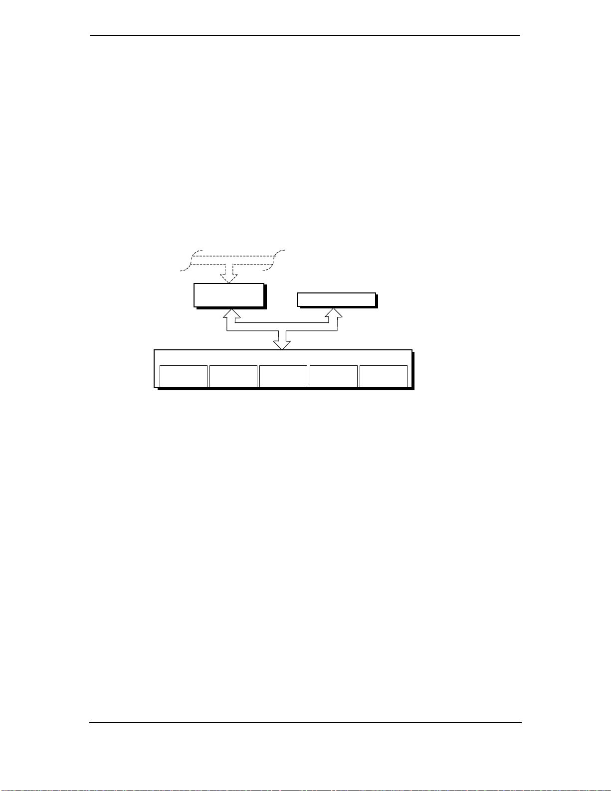
4.3 ISA BUS OVERVIEW
(2)
Technical Reference Guide
NOTE:
This section describes the ISA bus in general and highlights bus
implementation in this particular system. For detailed information regarding ISA bus
operation, refer to the Compaq Extended Industry Standard Architecture (EISA)
Technical Reference Guide.
The industr y standar d a rchitecture (ISA) bus provides an 8-/16-bit path for standard I/O
peripherals as well as for an optional device that can be installed in the ISA expansion slot (if
present). Figure 4-5 shows the key functions and devices that reside on the ISA bus.
PCI Bus
NOTE:
PCI/ISA
Bridge Function
Keyboard/
Mouse I/F
[1] Deskpro 4000S only
Diskette
I/F
8-/16-Bit ISA Bus
PC 87307 I/O Controller
Serial
I/F
ISA Connector [1]
Parallel
I/F
IrDA
I/F
Figure 4–5.
ISA Bus Bl oc k Diagram
Compaq Deskpro 4000N and 4000S Personal Computers
Firs t Edition - September1997
4-11
Page 54
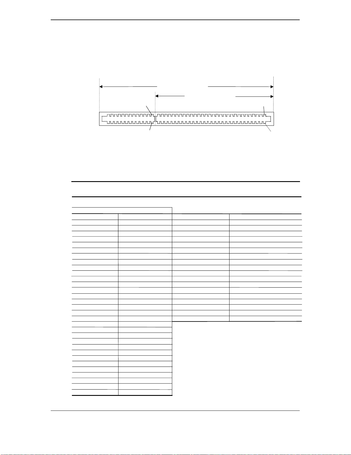
Chapter 4 System Support
4.3.1 ISA CONNECTOR
16-Bit ISA Connection
8-Bit ISA Connection
B1D1
C1
NOTE: See caution below.
Figure 4–6.
Table 4–7.
ISA Expansion Connector
ISA Expansion Connector Pinout
Table 4-7.
ISA Expansion Connector Pinout
16-Bit ISA Interface
8-Bit ISA Interface
Pin Signal Pin Signal Pin Signal Pin Signal
B01 GND A01 I/O CHK- D01 M16- C01 SBHEB02 RESDRV A02 SD7 D02 I/O16- C02 LA23
B03 +5 VDC A03 SD6 D03 IRQ10 C03 LA22
B04 IRQ9 A04 SD5 D04 IRQ11 C04 LA21
B05 -5 VDC A05 SD4 D05 IRQ12 C05 LA20
B06 DRQ2 A06 SD3 D06 IRQ15 C06 LA19
B07 -12 VDC A07 SD2 D07 IRQ14 C07 LA18
B08 NOWS- A08 SD1 D08 DAK0- C 08 LA17
B09 +12 VDC A09 SD0 D09 DRQ0 C09 MRDCB10 GND A10 BUSRDY D10 DAK5- C10 MWTCB11 SMWTC- A11 DMA D11 DRQ5 C11 SD8
B12 SMRDC- A12 SA19 D12 DAK6- C12 SD9
B13 IOWC- A13 SA18 D13 DRQ6 C13 SD10
B14 IORC- A14 SA17 D14 DAK7- C14 SD11
B15 DAK3- A15 SA16 D15 DRQ7 C15 SD12
B16 DRQ3 A16 SA15 D16 +5 VDC C16 SD13
B17 DAK1 A17 SA14 D17 GRAB- C17 SD14
B18 DRQ1 A18 SA13 D18 GND C18 SD15
B19 REFRESH- A19 SA12
B20 BCLK A20 SA11
B21 IRQ7 A21 SA10
B22 IRQ6 A22 SA9
B23 IRQ5 A23 SA8
B24 IRQ4 A24 SA7
B25 IRQ3 A25 SA6
B26 DAK2- A26 SA5
B27 T-C A27 SA4
B28 BALE A28 SA3
B29 +5 VDC A29 SA2
B30 OSC A30 SA1
B31 GND A31 SA0
CAUTION:
The maximum length for an
expansion card (PCI or ISA) installed in
this system is 7 inches. Longer cards may
be damaged or cause damage to t he
system.
A1
Compaq Deskpro 4000N and 4000S Personal Computers
4-12
Firs t Edition - September 1997
Page 55

4.3.2 ISA BUS TRANS ACTIONS
The ISA bus supports 8- and 16-bit transfers at an 8-MHz rate. Devices limited to 8-bit transfers
use the lower byte portion (data lines 7..0) while 16-bit transfers use the full bandwidth (data
lines 15..0). Addressing is handled by two classifications of address signals: latched and
latchable. Latched address signals ( SA19..0) select the specific byte within the 1-MB section of
memory defined by address lines LA23..17. Latchable address lin es (LA23..17) provide a longer
setup time for pre-chip selection or for pre-address decoding for high-speed memory and allow
access to up to 16-MB of physical memory on the ISA bus. The SA19..17 signals ha ve the same
values as the LA19..17 signals for all memory cycles. The I/O cycles use only the SA15..0
signals.
The key control signals are described as follows:
♦ MRDC- (Memory Read Cycle): MRDC- is active on all ISA memory reads accessing
memory from 000000h to FFFFFFh.
♦ SMEMR- (System Memory Read): SMEMR- is asserted by the PCI/ISA br idge to request an
ISA memory device to drive data onto the data lines for accesses below one megabyte.
SMEMR- is a delayed version of MRDC-.
♦ MWTC- (Memory Write Cycle): MWTC- is active on all ISA memory write cycles accessing
memory from 000000h to FFFFFFh.
♦ SMEMW- (System Memory Write): SMEMW- is asserted by the PCI/ISA br i d ge t o request
an I S A m emory device to accept data from the data lines for access below one megabyte.
SMEMW- is a delayed version of MWTC-.
♦ IORC- (Input/Output Read Cycle): IORC- commands an ISA I/O device to drive data onto
the data lines.
♦ IOWC- (Input/Output Write Cycle): IOWC- commands an ISA I/O device to accept data
from the data lines.
♦ SBHE- (System Byte High Enable): SBHE- indicates that a byte is being transferred on the
upper half (D15..8) of the data lines.
♦ SA0- (System Address Bit <0>): This bit is the complement of SBHE- and indicates that a
byte is being transferred on the lower half (D7..0) of the data lines.
♦ M16- (16-bit Memory Cycle): M16- is asserted by 16-bit ISA devices to indicate 16-bit
memory cycle capability.
♦ IO16- (16-bit I/O Cycle): IO16- is asserted by 16-bit ISA devices to indicate 16-bit I/O cycle
transfer capability.
Technical Reference Guide
If the a ddress on the SA li nes is a bove one mega byt e , SMRD C- and SMWTC- will not be active.
The MRDC- and MWTC- signals are active for memory accesses up to 16 megabytes and can be
used by any device that uses the full 16-bit ISA bus. To request a 16-bit transfer, a device asserts
either the M16- (memory) or IO16- (I/O) signal when the device is addressed.
When another device (such as a DMA d evice or another bus master ) t akes control of the ISA, the
Bus Address Latch Enable (BALE) signal is held active for the duration of the operation. As a
result , signals LA23..17 are always enabled and must be held stable for the duration of each bus
cycle.
When the address changes, devices on the bus may decode the latchable address (LA23..17) lines
and then latch them. This ar r a n gement allows devices to decode chip selects and M16- before the
next cycle actually begins.
Compaq Deskpro 4000N and 4000S Personal Computers
Firs t Edition - September1997
4-13
Page 56

Chapter 4 System Support
The following guidelines apply to optional ISA devices installed in the system:
♦ On bus lines that can be driven by a controller board, the driver should be able to sink a
minimum of 20 ma at 0.5 VDC and source 2 ma at 3.75 VDC.
♦ On bus lines that are driven in the low direction only (open collector), the driver should be
able to sink 20 ma at 0.5 VDC.
♦ The load on any logi c lin e from a single bus slot s hould not exceed 2 .0 ma in t he low state
(at 0.5 VDC) or 0.1 ma in the high state (at 3.75 VDC).
♦ The logic-high voltage at the bus ranges from 3.75 VDC to 5.5 VDC. The logic low voltage
ranges from 0 VDC to 0.8 VDC.
Compaq Deskpro 4000N and 4000S Personal Computers
4-14
Firs t Edition - September 1997
Page 57

4.3.3 DIRECT MEM O RY ACCESS
Direct Memory Access (DMA) is a m et hod by which an ISA device accesses system m em ory
without involving the micr oprocessor. DMA is n or mally used to transfer blocks of data to or from
an ISA I/O device. DMA reduces the amoun t of CPU int eraction s wit h memory, freeing th e CPU
for other processing tasks.
Technical Reference Guide
NOTE:
This section descri bes DMA in gener a l . For detailed information regarding
DMA operation, refer to the Compaq Extended Industry Standard Architecture (EISA)
Technical Reference Guide. Note, however, that EISA enhancements as described in the
referenced document ar e n ot supported in this (ISA only) system.
The South Bridge component i ncludes the equivalent of two 8237 DMA controllers cascaded
together to provide eight DMA chann els. T a ble 4-8 lists th e default configuration of the DMA
channels.
Table 4–8.
Default DMA Ch a nnel Assi g nment s
Table 4-8.
Default DMA Channel Assignments
DMA Channel Device ID
Controller 1 (byte transfers)
0
1
2
3
Controller 2 (word transfers)
4
5
6
7
Spare & ISA conn. pins D8, D9
Audio subsystem & ISA conn. pins B17, B18
Diskette drive & ISA conn. pins B6, B26
ECP LPT1 & ISA conn. pins B15, B16
Cascade for controller 1
Spare & ISA conn. pins D10, D11
Spare & ISA conn. pins D12, D13
Spare & ISA conn. pins. D14, D15
All cha nnels i n DMA controller 1 oper ate at a higher pr iority than those in controller 2 . Note
that channel 4 is not available for use other than its cascading function for controller 1. The
DMA controll er 2 can transfer words only on an even addr ess bound a ry. The DMA cont roller
and page register define a 24-bit address that allows data transfers within the address space of
the CPU. The DMA contr oll ers operate a t 8 MHz.
The DMA l ogi c is accessed throug h two types of I/O mapped registers; pa g e regist ers an d
controller registers. The mapping is th e same regardless of the support chipset used.
Compaq Deskpro 4000N and 4000S Personal Computers
Firs t Edition - September1997
4-15
Page 58

Chapter 4 System Support
4.3.3.1 Page Registers
The DMA pag e register con tain s the eight most significant bits of the 24-bit address and works
in conjunction with the DMA controllers to define the complete (24-bit)address for the DMA
channels. T able 4-9 lists th e page register port a ddresses.
Table 4–9.
DMA Page Register Ad dresses
Table 4-9.
DMA Channel Page Register I/O Port
Controller 1 (byte transfers)
Ch 0
Ch 1
Ch 2
Ch 3
Controller 2 (word transfers)
Ch 4
Ch 5
Ch 6
Ch 7
Refresh 08Fh [see note]
NOTE:
The DMA memory page register for the refresh channel must be
programmed with 00h for proper operation.
DMA Page Register Addr es s es
087h
083h
081h
082h
n/a
08Bh
089h
08Ah
The memory address is derived as follows:
24-Bit Address - Controller 1 (Byte Tran sfers)
8-Bit Page Register 8-Bit DMA Con t roller
A23..A16 A15..A00
24-Bit Address - Controller 2 (Word Transfers)
8-Bit Page Register 16-Bit DMA Controller
A23..A17 A16..A01, (A00 = 0)
Note that a d d ress lin e A16 fr om the DMA memor y page register is disabled when DMA
controll er 2 is selected. Add ress line A00 is not con nected to DMA controller 2 a nd is al ways 0
when wor d -len g th t ransfers are selected.
By not connecting A00, the following applies:
♦ The size of the the block of data that can be moved or addressed is measured in 16-bits
(words) rather tha n 8-bits (bytes).
♦ The words must always be addressed on an even boundary.
DMA controll er 1 can move up to 64 Kbytes of data per DMA transfer. DMA cont roller 2 can
move up to 64 Kwords (128 Kbytes) of data per DMA tra nsfer. Word DMA oper ations are only
possible between 16-bit memory and 16-bit peripherals.
Compaq Deskpro 4000N and 4000S Personal Computers
4-16
Firs t Edition - September 1997
Page 59

The RAM refresh is designed to perform a memory read cycle on each of the 512 row addresses
in the DRAM memory space. Refresh operations are used to refresh memory on the 32-bit
memory bus and the ISA bus. The refresh addr ess is provided on lines SA00 through SA08.
Address lines LA23..17, SA18,19 are driven low.
The remaining address lines are in an undefined state during the refresh cycle. The refresh
operations are driven by a 69.799-KHz clock generated by Interval Timer 1, Counter 1. The
refresh rate is 128 refresh cycles in 2.038 ms.
4.3.3.2 DMA Controller Registers
Table 4-10 lists th e DMA Cont roller Registers and their I/O port addresses. Note that there is a
set of register s for each DMA contr oller.
Technical Reference Guide
Table 4–10.
DMA Contr oll er Registers
Table 4-10.
DMA Controller Regist er s
Register Controller 1 Controller 2 R/W
Status 008h 0D0h R
Command 008h 0D0h W
Mode 00Bh 0D6h W
Write Single Mask Bit 00Ah 0D4h W
Write All Mask Bits 00Fh 0 DEh W
Software DRQx Request 009h 0D2h W
Base and Current Address - Ch 0 000h 0C0h W
Current Address - Ch 0 000h 0C0h R
Base and Current Word Count - Ch 0 001h 0C2h W
Current Word Count - Ch 0 001h 0C2h R
Base and Current Address - Ch 1 002h 0C4h W
Current Address - Ch 1 002h 0C4h R
Base and Current Word Count - Ch 1 003h 0C6h W
Current Word Count - Ch 1 003h 0C6h R
Base and Current Address - Ch 2 004h 0C8h W
Current Address - Ch 2 004h 0C8h R
Base and Current Word Count - Ch 2 005h 0CAh W
Current Word Count - Ch 2 005h 0CAh R
Base and Current Address - Ch 3 006h 0CCh W
Current Address - Ch 3 006h 0CCh R
Base and Current Word Count - Ch 3 007h 0CEh W
Current Word Count - Ch 3 007h 0CEh R
Temporary (Command) 00Dh 0DAh R
Reset Pointer Flip-Flop (Command) 00Ch 0D8h W
Master Reset (Command) 00Dh 0DAh W
Reset Mask Register (Command) 00Eh 0DCh W
NOTE:
For a detailed description of the DMA registers, refer to the
Compaq EISA Technical Reference Guide
.
Compaq Deskpro 4000N and 4000S Personal Computers
Firs t Edition - September1997
4-17
Page 60

Chapter 4 System Support
4.3.4 INTERRUPTS
The microprocessor uses two types of interrupts; maskable and nonmaskable. A maskable
interrupt can be enabled or disabled within the microprocessor by the use of the STI and CLI
instructions. A nonmaskable interrupt cannot be masked off within the microprocessor but may
be inhibited by hardware or software means external to the microprocessor.
4.3.4.1 Maskab le In t e rrupt s
The maskable interrupt is a hardware-generated signal used by peripheral functions within the
system to get the attention of the microprocessor. Peripheral functions produce a unique INTA-D
(PCI) or IRQ0-15 (ISA) signal that is routed to interrupt processing logic that asserts the
interrupt (INTR) input to the microprocessor. The microprocessor halts execution to determine
the source of the interrupt and then services the peripheral as appropriate.
ISA Peripherals
& SM Functions
PCI Peripherals
Figure 4–7.
The South Bridge component, which includes the equivalent of two 8259 interrupt controllers
cascaded together, handles the standard AT-type (ISA) interrupt signals (IRQn). The South
Brid g e also r eceives th e PCI inter rupt signal s ( P I RQA - ..PIRQD - ) from PCI d evi ces . Th e P C I
interrupts can be configured by PCI Configuration Registers 55h..57h to share the standard ISA
interrupts (IRQn). The power-up default configuration has the PIRQn disabled. Table 4-11 lists
the standard source configuration for maskable interrupts and their priorities. If more than one
interrupt is pending, the highest priority (lowest number) is processed first.
IRQ1,3..7,
9..12,
14,15
PIRQA-..D-
South Bridge Component
IRQ1,3..7
PCI IRQ
Routing
IRQ9..12,
14,15
Interrupt
Cntlr. 2
IRQ2
Maskable Interrupt Pr ocessing, Block Diagram
Interrupt
Cntlr. 1
INTR
Microprocessor
Compaq Deskpro 4000N and 4000S Personal Computers
4-18
Firs t Edition - September 1997
Page 61

Technical Reference Guide
Table 4–11. Maskable Interrupt Priorities and Assignments
Table 4-11.
Maskable Interrupt Priorities and Assignments
Priority Signal Label Source (Typical) Notes
1 IRQ0 Interval timer 1, counter 0
2 IRQ1 Keyboard
3 IRQ8- Real-time clock
4 IRQ9 Spare and ISA connector pin B04
5 IRQ10 Spare and ISA connector pin D03
6 IRQ11 Spare and ISA connector pin D04
7 IRQ12 Mouse and ISA connector pin D05
8 IRQ13 Coprocessor (math)
9 IRQ14 IDE primary I/F and ISA connector pin D07
10 IRQ15 IDE secondary I/F and ISA connector pin D06
11 IRQ3 Serial port (COM2) and ISA connector pin B25
12 IRQ4 Serial port (COM1) and ISA connector pin B24
13 IRQ5 Audio su bsystem and ISA connector pin B23
14 IRQ6 Diskette drive controller and ISA connector pin B22
15 IRQ7 Parallel port (LPT1)
-- IRQ2 NOT AVAILABLE (Cascade from interrupt controller 2)
NOTE:
[3] Alternate available interrupts: IRQ5, 9,10,11,14, or 15
Interrupt s gener a ted by PCI devices can be configured to share the standard AT (IRQn) int er rupt
lines. Refer to section 4.2.5 “PCI Interrupt Mapping” for information on PCI interrupts.
Maskable Interrupt processing is controlled and monitored through standard AT-type I/Omapped registers. These registers ar e listed in Table 4-12.
Table 4–12. Maskable Interrupt Cont rol Registers
Table 4-12.
Maskable Interr upt Control Registers
I/O Port Register
020h Base Address, Int. Cntlr. 1
021h Initialization Command Word 2-4, Int. Cntlr. 1
0A0h Base Address, Int. Cntlr. 2
0A1h Initialization Command Word 2-4, Int. Cntlr. 2
The initialization and operation of the interrupt control registers follows standard AT-type
protocol.
Compaq Deskpro 4000N and 4000S Personal Computers
Firs t Edition - September1997
4-19
Page 62

Chapter 4 System Support
4.3.4.2 Non-Maskable Interrupts
Non-maskble interrupts cannot be masked (inhibited) within the microprocessor itself but may be
maskable by software using logic external to the microprocessor. There are two nonmaskable
interrupt signals: the NMI- and the SMI-. These signals have service priority over all maskable
interrupts, with the SMI- having top priority over all interrupts including the NMI-.
NMI- Generation
The Non-Maskable Interrupt (NMI-) signa l can be generated by one of the following actions:
♦ Parity errors detected on the ISA bus (activating IOCHK-).
♦ Parity errors detected on a PCI bus (activating SERR- or PERR-).
♦ Microprocessor internal error (activating IERRA or IERRB)
The IOCHK-, SERR-, and PERR- signals are routed through the south bridge component, which
in turn activates the NMI to the microprocessor.
The NMI Status Register at I/O port 061h contains NMI source and status data as follows:
NMI Status Register 61h
Bit Function
7 NMI Status:
0 = No NMI from system board parity error.
1 = NMI requested, read only
6 IOCHK- NMI:
0 = No NMI from IOCHK-
1 = IOCHK- is active (low), NMI requested, read only
5 Interval Timer 1, Counter 2 (Speaker) Status
4 Refresh Indicator (toggles with every refresh)
3 IOCHK- NMI Enable/Disable:
0 = NMI from IOCHK- enabled
1 = NMI from IOCHK- disabled and cleared (R/W)
2 System Board Parity Error (PERR/SERR) NMI Enable:
0 = Parity error NMI enabled
1 = Parity error NMI disabled and cleared (R/W)
1 Speaker Data (R/W)
0 Inteval Timer 1, Counter 2 Gate Signal (R/W)
0 = Counter 2 disabled
1 = Counter 2 enabled
Functions not related to NMI activity.
After the active NMI has been processed, status bits <7> or <6> are cleared by pulsing bits <2>
or <3> respectively.
The NMI Enable Register (070h, <7>) is used to enable/disable the NMI signal. Writing 80h to
this register masks generation of the NMI-. Note that the lower six bits of register at I/O port 70h
affect RTC operation and should be considered when changing NMI- generation status.
Compaq Deskpro 4000N and 4000S Personal Computers
4-20
Firs t Edition - September 1997
Page 63

Technical Reference Guide
SMI- Generation
The SMI- (System Management Interrupt) is typically used for power management functions.
When power management is enabled, inactivity timers are monitored. When a timer times out,
SMI- is asserted and invokes the microprocessor’s SMI handler. The SMI- handler works with
the APM BIOS to service the SMI- accordi ng to th e cau se of th e timeout.
Although the SMI- is primarily used for power managment the interrupt is also employed for the
QuickLock/QuickBlank functions as well.
Compaq Deskpro 4000N and 4000S Personal Computers
Firs t Edition - September1997
4-21
Page 64

Chapter 4 System Support
4.3.5 INTERVAL TIMER
The interval timer generates pulses at software (programmable) intervals. A 8254-compatible
timer is integrated into the South Bridge chip. The timer function provides three counters, the
functions of which ar e listed in T able 4-13.
Table 4–13.
Interval Timer Functions
Table 4-13.
Interval Tim er Functions
Counter Function Gate Clock In Clock Out
0 System Clock Always on 1.193 MHz IRQ0
1 Refresh Always on 1.193 MHz Refresh Req.
2 Speaker Tone Port 61, bit<0> 1.193 MHz Speaker Input
The interval timer is controlled through the I/O mapped registers listed in Table 4-14.
Table 4–14.
Interval Timer Control Registers
Table 4-14.
Interval Timer Control Registers
I/O Port Register
040h Read or write value, counter 0
041h Read or write value, counter 1
042h Read or write value, counter 2
043h Control Word
Interval timer operation follows standard AT-type protocol. For a detailed description of timer
registers and operation, refer to the Compaq Extended Industry Standard Architecture Expansion
Bus Technical Reference Guide.
4.3.6 ISA CONFIGURATION
The working relationship between the PCI and ISA buses requires that certain parameters be
configured. The PC/ISA bridge function of the South Bridge component includes configuration
registers to set parameters such as PCI IRQ routing and top-of-memory available to ISA/DMA
devices. These parameters are programmed by BIOS during power-up, using registers listed
previously in Table 4-6.
Compaq Deskpro 4000N and 4000S Personal Computers
4-22
Firs t Edition - September 1997
Page 65

4.4 SYSTEM CLOCK DISTRIB UTION
The system uses an ICS9147-08 or compatible part for generation of most clock signals. Tables
4-15 lists the clock signals and to which components they are distributed.
Technical Reference Guide
Table 4–15.
Clock Generation and Distribution (Pentium-Based System)
Table 4-15.
Clock Generation and Distribution
Signal Frequency Source Destination
CPUCLK 60/66 MHz [1] ICS9147 CPU, VT82C595
CACHE_CLKn CPUCLK “ L2 SRAMs
DIMMn_CLKn CPUCLK “ DIMMs
PCICLK CPUCLK/2 “ PCI slots
LRU_CLK CPUCLK/2 “ Compaq ASIC
TLAN_CLK CPUCLK/2 “ TLAN ASIC
PCI Bridge Clock CPUCLK/2 “ VT82C595, VT82C586
SIO/USB CLK 48 MHz “ 87307, VT82C586
PHYCLK 25 MHz Crystal LXT970
TLAN 20 MHz “ TLAN ASIC
Crystal CLK 14.318 MHz Crystal ICS9147
CLK_14 14 MHz ICS9147 [2] ISA bus, VT82C586,
BCLK PCICLK/4 [3] VT82C586 ISA bus
NOTES:
[1] Depending on speed configuration (refer to Chapter 3, “Processor/Memory Subsystem”).
[2] Routed through buffer before destination.
[3] 8.33 MHz if PCICLK = 33 MHz, 7.5 MHz if PCICLK = 30 MHz
ESS1868
Compaq Deskpro 4000N and 4000S Personal Computers
Firs t Edition - September1997
4-23
Page 66

Chapter 4 System Support
4.5 REAL-TIME CLOCK AND CONFIGURATION MEMORY
The Real-time clock (RTC) and configuration memory functions are provided by the PC87307
I/O controller. The RTC uses the first 14 of 256 bytes of configuration memory and is
MC146818-compatible. As shown in the following figure, the 87307 controller provides 256
bytes of configuration memory, divided into two 128-byte banks. The RTC/configuration memory
can be accessed using conventional OUT and IN assembly language instructions using I/O ports
70h/71h, alth ough th e suggested method is to use the INT15 AX=E823h BIOS call.
87307
Upper Config.
Memory Area
(128 bytes)
Lower Config.
Memory Area
(114 bytes)
RTC Area
(14 bytes)
FFh
80h
7Fh
0Eh
0Dh
00h
Figure 4–8.
NOTE:
Non-volatile (NVRAM) storage of PCI, ESCD, and Environmental Variable (EV) data
0Dh
0Ch
0Bh
0Ah
09h
08h
07h
06h
05h
04h
03h
02h
01h
00h
Register D
Register C
Register B
Register A
Year
Month
Date of Month
Day of Week
Hours (Alarm)
Hours (Timer)
Minutes (Alarm)
Minutes (Timer)
Seconds (Alarm)
Seconds (Timer)
Configuration Memory Map
is provided by portions of the 256-KB system BIOS ROM component.
A 3-VDC battery is used for maintaining the RTC and configuration memory while the system is
powered down. This battery is soldered on the system board and is designed to last from 5-7
years. Once expired, the soldered battery is by-passed by connecting a replacement battery
(Compaq p/n 160274-001 or equivalent 4.5 VDC @ 660 ma alkaline battery) to header P14 pins
9-12. On-board logic regulates the external battery voltage to 3 VDC.
The configuration memory (including the password) can be cleared by moving the jumper from
P14 pins 1 and 2 to pins 2 and 3 for at least one minute while unit power ids off. The password
can be disabled by switching DIP SW1-1 on.
Compaq Deskpro 4000N and 4000S Personal Computers
4-24
Firs t Edition - September 1997
Page 67

4.5.1 CONFIGURATION MEM ORY BYTE DEFINITIONS
Table 4-16 lists the mapping of the configuration memory.
Technical Reference Guide
Table 4–16.
Configuration Memory (CMOS) Map
Table 4-16.
Configuration Memory ( CM OS) Map
Location Function Location Function
00-0Dh Real-rime clock 41h-44h Hoof Removal Time Stamp
0Eh Diagnostic status 45h Keyboard snoop byte
0Fh System reset code 46h Diskette drive status
10h Diskette drive type 47h Last IPL device
11h Reserved 48h-4Bh IPL priority
12h Hard drive type 4Ch-4Fh BVC priority
13h Security functions 51h ECC DIMM status
14h Equipment installed 52h Board revision (from boot block)
15h Base memory size, low byte/KB 53h SWSMI command
16h Base memory size, high byte/KB 54h SWSMI data
17h Extended memory, low byte/KB 55h APM command
18h Extended memory, high byte/KB 56h Erase-Ease keyboard byte
19h Hard drive 1, primary controller 57h-76H Saved CMOS location 10h-2Fh
1Ah Hard drive 2, primary controller 77h-7Fh Administrator password
1Bh Hard drive 1, secondary controller 80h ECMOS diagnostic byte
1Ch Hard drive 2, secondary controller 81h-82h Total super ext. memory tested good
1Dh Enhanced hard drive support 83h Microprocessor chip ID
1Eh Reserved 84h Microprocessor chip revision
1Fh Power management functions 85h Hood removal status byte
24h System board ID 86h Fast boot date
25h System architecture data 87h Fast boot status byte
26h Auxiliary peripheral configuration 8Dh-8Fh POST error logging
27h Speed control external drive 90h-91h Total super extended memory configured
28h Expanded/base mem. size, IRQ12 92h Miscellaneous configuration byte
29h Miscellaneous configuration 93h Miscellaneous PCI features
2Ah Hard drive timeout 94h ROM flash/power button status
2Bh System inactivity timeout 97h Asset/test prompt byte
2Ch Monitor timeout, Num Lock Cntrl 9Bh Ultra-33 DMA enable byte
2Dh Additional flags 9Ch Mode-2 Configuration
2Eh-2Fh Checksum o f locations 10h-2Dh 9Dh ESS audio configuration
30h-31h Total extended memory tested 9Eh ECP DMA configuration
32h Century 9Fh-AFh Serial number
33h Miscellaneous flags set by BIOS B0h-C3h Custom drive types 65, 66, 68, 15
34h International language C7h Serial port 1 address
35h APM status flags C8h Serial port 2 address
36h ECC POST test single bit C9h COM1/COM2 port configuration
37h-3Fh Power-on password DEh-DFh Checksum o f locations 90h to DDh
40h Miscellaneous Disk Bits E0h-FFh Client Management error log
NOTE: Assume unmarked gaps are reserved.
Default values (where applicable) are given for a standard system as shipped from the factory.
The contents of configuration memory can be cleared by the following jumper positioning:
RTC using internal battery:
Move jumper on header E50 from pins 1 and 2 to pins 2 and 3.
RTC using external battery:
Move jumper on header E50 from pins 2 and 3 to pins 1 and 2.
Compaq Deskpro 4000N and 4000S Personal Computers
Firs t Edition - September1997
4-25
Page 68
Chapter 4 System Support
RTC Control Register A, B y t e 0 Ah
Bit Function
7 Update in Progress. Read only.
0 = Time update will not occur before 2444 us
1 = Time update will occur within 2444 us
6..4 Divider Chain Control. R/W.
00x = Oscillator disabled.
010 = Normal operation (time base frequency = 32.768 KHz).
11x = Divider chain reset.
3..0 Periodic Interrupt Control. R/W. Specifies the periodic interrupt inte rval.
0000 = none 1000 = 3.90625 ms
0001 = 3.90625 ms 1001 = 7.8125 ms
0010 = 7.8125 ms 1010 = 15. 625 ms
0011 = 122.070 us 1011 = 31.25 ms
0100 = 244.141 us 1100 = 62.50 ms
0101 = 488.281 us 1101 = 125 ms
0110 = 976.562 us 1110 = 250 ms
0111 = 1.953125 ms 1111 = 500 ms
RTC Control Register B, Byte 0Bh
Bit Function
7 Time Update Enable/disable
0 = Normal operation, 1 = Disable time updating for time set
6 Periodic Interrupt Enable/Disable.
0 = Disable, 1 = Enable interval specified by Register A
5 Alarm Interrupt Enable/disable
0 = Disabled, 1 = Enabled
4 End-of-Update Interrupt Enable/Disable
0 = Disabled, 1 = Enabled
3 Reserved (read 0)
2 Time/Date Format Select
0 = BCD format, 1 = Binary format
1 Time Mode
0 = 12-lhour mode, 1 = 24-hour mode
0 Automatic Daylight Savings Time Enable/Disable
0 = Disable
1 = Enable (Advance 1 hour on 1
st
Sunday in April, retreat 1 hour on last Sunday in October).
RTC Status Register C, Byte 0Ch
Bit Function
7 If set, interrupt output signal active (read only)
6 If set, indicates periodic interrupt flag
5 If set, indicates alarm interrupt
4 If set, indicates end-of-update interrupt
3..0 Reserved
RTC Status Register D, Byte 0Dh
Bit Function
7 RTC Power Status
0 = RTC has lost power
1 = RTC has not lost power
6..0 Reserved
Compaq Deskpro 4000N and 4000S Personal Computers
4-26
Firs t Edition - September 1997
Page 69

Configuration Byte 0Eh, Diagnostic Status
Default Value = 00h
This byte contains diagnostic status data.
Configuration Byt e 0 Fh, Sy stem Reset Code
Default Value = 00h
This byte contains the system reset code.
Configuration Byte 10h, Diskette Drive Type
Bit Function
7..4 Primary (Drive A) Diskette Drive Type
3..0 Secondary (Drive B) Diskette Drive Type
Valid values for bits <7..4> and bits <3..0>:
0000 = Not installed
0001 = 360-KB drive
0010 = 1.2-MB drive
0011 = 720-KB drive
0100 = 1.44-MB/1.25-MB drive
0110 = 2.88-MB drive
(all other values reserved)
Technical Reference Guide
Configuration Byte 12h, Hard Drive Type
Bit Function
7..4 Primary Controller 1, Hard Drive 1 Type:
0000 = none 1000 = Type 8
0001 = Type 1 1001 = Type 9
0010 = Type 2 1010 = Type 10
0011 = Type 3 1011 = Type 11
0100 = Type 4 1100 = Type 12
0101 = Type 5 1101 = Type 13
0110 = Type 6 1110 = Type 14
0111 = Type 7 1111 = other (use bytes 19h)
3..0 Primary Controller 1, Hard Drive 2 Type:
0000 = none 1000 = Type 8
0001 = Type 1 1001 = Type 9
0010 = Type 2 1010 = Type 10
0011 = Type 3 1011 = Type 11
0100 = Type 4 1100 = Type 12
0101 = Type 5 1101 = Type 13
0110 = Type 6 1110 = Type 14
0111 = Type 7 1111 = other (use bytes 1Ah)
Compaq Deskpro 4000N and 4000S Personal Computers
Firs t Edition - September1997
4-27
Page 70
Chapter 4 System Support
Configuration Byte 13h, Security Functions
Default Value = 00h
Bit Function
7 Reserved
6 QuickBlank Enable After Standby:
0 = Disable
1 = Enable
5 Administrator Password:
0 = Not present
1 = Present
4 Reserved
3 Diskette Boot Enable:
0 = Enable
1 = Disable
2 QuickLock Enable:
0 = Disable
1 = Enable
1 Network Server Mode/Security Lock Override:
0 = Disable
1 = Enable
0 Password State (Set by BIOS at Power-up)
0 = Not set
1 = Set
Configuration Byte 14h, Equipment Installed
Default Value (standard configuration) = 03h
Bit Function
7,6 No. of Diskette Drives Installed:
00 = 1 drive 10 = 3 drives
01 = 2 drives 11 = 4 drives
5..2 Reserved
1 Coprocessor Present
0 = Coprocessor not installed
1 = Coprocessor installed
0 Diskette Drives Present
0 = No diskette drives installed
1 = Diskette drive(s) installed
Configuration Bytes 15h and 16h, Base Memory Size
Default Value = 280h
Bytes 15h and 16h hold a 16-bit value that specifies the base memory size in increments of 1-KB
(1024) bytes. Valid base memory sizes are 512-KB and 640-KB.
Configuration Bytes 17h and 18h, Extended Memory Size
Bytes 17h and 18h hold a 16-bit value that specifies the extended memory size in increments of
1-KB (1024) bytes.
Compaq Deskpro 4000N and 4000S Personal Computers
4-28
Firs t Edition - September 1997
Page 71
Technical Reference Guide
Configuration Bytes 19h-1Ch, Hard Drive Types
Byte 19h contains the hard drive type for drive 1 of the primary controller if byte 12h bits <7..4>
hold 1111b. Byte 1Ah contains the hard drive type for drive 2 of the primary controller if byte
12h bits <3..0> hold 1111b. Bytes1Bh and 1Ch contain the har d drive types for hard drives 1 and
2 of the secondary controller.
Configuration Byt e 1 Dh, Enhanced IDE Hard Drive Support
Default Value = F0h
Bit Function
7 EIDE - Drive C (83h)
6 EIDE - Drive D (82h)
5 EIDE - Drive E (81h)
4 EIDE - Drive F (80h)
3..0 Reserved
Values for bits <7..4> :
0 = Disable
1 = Enable for auto-configure
Configuration Byte 1Fh, Power Management Functions
Default Value = 00h
Bit Function
7..4 Reserved
3 Slow Processor Clock for Low Power Mode
0 = Processor runs at full speed
1 = Processor runs at slow speed
2 Reserved
1 Monitor Off Mode
0 = Turn monitor power off after 45 minutes in standby
1 = Leave monitor power on
0 Energy Saver Mode Indicator (Blinking LED)
0 = Disable
1 = Enable
Configuration Byt e 2 4 h, Sy st e m B oar d Ide nt i f i cation
Default Value = 7Eh
Configuration memory location 24h holds the system board ID.
Configuration Byte 25h, System Architecture Data
Default Value = 0Bh
Bit Function
7..4 Reserved
3 Unmapping of ROM:
0 = Allowed
1 = Not allowed
2 Reserved
1,0 Diagnostic Status Byte Address
00 = Memory locations 80C00000h-80C00004h
01 = I/O ports 878h-87Ch
11 = neither place
Compaq Deskpro 4000N and 4000S Personal Computers
Firs t Edition - September1997
4-29
Page 72
Chapter 4 System Support
Configuration Byte 26h, Auxiliary Peripheral Configuration
Default Value = 00h
Bit Function
7,6 I/O Delay Select
00 = 420 ns (default)
01 = 300 ns
10 = 2600 ns
11 = 540 ns
5 Alternative A20 Switching
0 = Disable port 92 mode
1 = Enable port 92 mode
4 Bi-directional Print Port Mode
0 = Disabled
1 = Enabled
3 Graphics Type
0 = Color
1 = Monochrome
2 Hard Drive Primary/Secondary Address Select:
0 = Primary
1 = Secondary
1 Diskette I/O Port
0 = Primary
1 = Secondary
0 Diskette I/O Port Enable
0 = Primary
1 = Secondary
Configuration Byte 27h, Speed Control/External Drive
Default Value = 00h
Bit Function
7 Boot Speed
0 = Max MHz
1 = Fast speed
6..0 Reserved
Configuration Byte 28h, Expanded and Base Memory, IRQ12 Select
Default Value = 00h
Bit Function
7 IRQ12 Select
0 = Mouse
1 = Expansion bus
6,5 Base Memory Size:
00 = 640 KB
01 = 512 KB
10 = 256 KB
11 = Invalid
4..0 Internal Compaq Memory:
00000 = None
00001 = 512 KB
00010 = 1 MB
00011 = 1.5 MB
.
.
11111 = 15.5 MB
Configuration Byte 29h, Miscellaneous Configuration Data
Compaq Deskpro 4000N and 4000S Personal Computers
4-30
Firs t Edition - September 1997
Page 73
Default Value = 00h
Bit Function
7..5 Reserved
4 Primary Hard Drive Enable (Non-PCI IDE Controllers)
0 = Disable
1 = Enable
3..0 Reserved
Configuration Byte 2Ah, Hard Drive Timeout
Default Value = 02h
Bit Function
7..5 Reserved
4..0 Hard Drive Timeout
00000 = Disabled
00001 = 1 minute
00010 = 2 minutes
.
.
10101 = 21 minutes
Configuration Byte 2Bh, System Inactivity Timeout
Default Value = 23h
Bit Function
7 Reserved
6,5 Power Conservation Boot
00 = Reserved
01 = PC on
10 = PC off
11 = Reserved
4..0 System Inactive Timeout. (Index to SIT system tim eout record)
00000 = Disabled
Technical Reference Guide
Configuration Byte 2Ch, ScreenSave and NUMLOCK Control
Default Value = 00h
Bit Function
7 Reserved
6 Numlock Control
0 = Numlock off at power on
1 = Numlock on at power on
5 Screen Blank Control:
0 = No screen blank
1 = Screen blank w/QuickLock
4..0 ScreenSave Timeout. (Index to SIT monitor timeout record)
000000 = Disabled
Compaq Deskpro 4000N and 4000S Personal Computers
4-31
Firs t Edition - September1997
Page 74

Chapter 4 System Support
Configuration Byt e 2 Dh, Additional Fla g s
Default Value = 00h
Bit Function
7..5 Reserved
4 Memory Test
0 = Test memory on power up only
1 = Test memory on warm boot
3 POST Error Handling (BIOS Defined)
0 = Display “Press F1 to Continue” on error
1 = Skip F1 message
2..0 Reserved
Configuration Byte 2Eh, 2Fh, Checksum
These bytes hold the checksum of bytes 10h to 2Dh.
Configuration Byte 30h, 31h, Total Extended Memory Tested
This location holds the amount of system memory that checked good during the POST.
Configuration Byte 32h, Century
This location holds the Century value in a binary coded decimal (BCD) format.
Configuration Byte 33h, Miscellaneous Flags
Default Value = 80h
Bit Function
7 Memory Above 640 KB
0 = No, 1 = Yes
6 Reserved
5 Weitek Numeric Coprocessor Present:
0 = Not installed, 1 = Installed
4 Standard Numeric Coprocessor Present:
0 = Not installed, 1 = Installed
3..0 Reserved
Configuration Byte 34h, International Language Support
Default Value = 00h
Compaq Deskpro 4000N and 4000S Personal Computers
4-32
Firs t Edition - September 1997
Page 75

Configuration Byte 35h, APM Status Flags
Default Value = 11h
Bit Function
7..6 Power Conservation State:
00 = Ready
01 = Standby
10 = Suspend
11 = Off
5,4 Reserved
3 32-bit Connection:
0 = Disconnected, 1 = Connected
2 16-bit Connection
0 = Disconnected, 1 = Connected
1 Real Mode Connection
0 = Disconnected, 1 = Connected
0 Power Management Enable:
0 = Disabled
1 = Enabled
Technical Reference Guide
Configuration Byt e 3 6 h, E CC PO ST T e st Si ng l e Bit E r r ors
Default Value = 01h
Bit Function
7 Row 7 Error Detect
6 Row 6 Error Detect
5 Row 5 Error Detect
4 Row 4 Error Detect
3 Row 3 Error Detect
2 Row 2 Error Detect
1 Row 1 Error Detect
0 Row 0 Error Detect
0 = No single bit error detected.
1 = Single bit error detected.
Configuration Byt e 3 7 h-3 Fh, Power -On Password
These eight locations hold the power-on password.
Configuration Byte 40h, Miscellaneous Disk Data
Configuration Bytes 41h-44h, Hood Removal Time Stamp
These four bytes record the time at which the hood of the system was removed:
Byte 41h, month & day
Byte 42h, year and month
Byte 43h, min ut es an d seconds
Byte 44h, removal flag and minutes
Compaq Deskpro 4000N and 4000S Personal Computers
Firs t Edition - September1997
4-33
Page 76

Chapter 4 System Support
Configuration Byte 45h, Keyboard Snoop Data
Default Value = xxh
Bit Function
7 Cntrl/F10 Key Status:
0 = Cntrl & F10 keys not pressed
1 = Cntrl & F10 keys pressed
6 F10 Key Status:
0 = F10 key not pressed
1 = F10 key pressed
5..1 Reserved
0 Key Pressed Flag:
0 = Key not pressed
1 = Key pressed
Configuration Byte 46h, Diskette/Hard Drive Status
Default Value = xxh
Bit Function
7,6 Reserved
5 Partition On HD:
0 = Not set, 1 = Set
4 Setup Disk:
0 = Not present, 1 = Present
3 ROMPAQ or DIAGS Diskette:
0 = Not present, 1 = Present
2 Boot Diskette in Drive A:
0 = No, 1 = Yes
1 Drive B: Present:
0 = Not present, 1 = Present
0 Drive A: Present:
0 = Not present, 1 = Present
Configuration Bytes 47h-4Fh, IPL Data
These bytes hold initial program load (IPL) data for boot purposes :
Byte 47h, last IPL device
Bytes 48h-4Bh, IPL priority
Byte 4Ch-4Fh, BCV priorit y
Configuration Byte 51h, ECC Status Byte
Default Value = xxh
Bit Function
7 ECC Status for DIMM 3
6 ECC Status for DIMM 2
5 ECC Status for DIMM 1
4 ECC Status for DIMM 0
3..0 Reserved
Compaq Deskpro 4000N and 4000S Personal Computers
4-34
Firs t Edition - September 1997
Page 77

Configuration Byte 52h, Board Revision
This byte hol ds the boa rd revision as copi e d from the boot block s e c tor.
Configuration Byte 53h, 54h, SW SMI Command/Data Bytes
Configuration Byte 55h, APM Command Byte
Configuration Byte 56h, Miscellaneous Flags Byte
Bit Function
7 CAS Latency:
0 = 2, 1 = 3
6 IR Port Enable Flag:
0 = Disabled (COM2 config. for standard serial port)
1 = Enabled (COM2 config. for IrDA)
5 Warm Boot Enable Flag:
0 = Disable, 1 = Enable
4 POST Terse/Verbose Mode
0 = Verbose, 1 = Terse
3..1 Erase Ease Keyboard Mode:
000 = Backspace/Spacebar
001 = Spacebar/Backspace
010 = Spacebar/Spacebar
011-111 = Invalid
0 Configurable Power Supply:
0 = Power switch active
1 = Power switch inhibited
Technical Reference Guide
Configuration Byte 57h-76h, CMOS Copy
Configuration Byt e s 7 7 h-7 Fh, Admini st r a t or Password
Configuration Byte 80h, CMOS Diagnostic Flags Byte
Default Value = 00h. Set bit indicates function is valid.
Bit Function
7 CMOS Initialization (Set CMOS to Default)
6 Setup password locked
5 PnP should not reject SETs because Diags is active
4 Reserved
3 Manufacturing diagnostics diskette found
2 Invalid electronic serial number
1 Boot maintenance partition once
0 Invalid CMOS checksum
Configuration Byte 81h, 82h, Total Super Extended Memory Tested
This byte holds the value of the amount of extended system memory that tested good during
POST. The am oun t is gi ven in 64-KB increment s.
Compaq Deskpro 4000N and 4000S Personal Computers
Firs t Edition - September1997
4-35
Page 78

Chapter 4 System Support
Configuration Byte 83h, Microprocessor Identification
This byte holds the component ID and chip revision of the microprocessor.
Configuration Byte 84h, Microprocessor Revision
Configuration Byte 85h, Hood Lock/Administration Mode
Bit Function
7,6 Reserved
5 ESCD Buffering:
0 = No buffering, 1 = ESCD buffered at F000h.
4 Hood Lock Enable:
0 = Disabled, 1 = Enabled
3 User Mode Flag
2 Administration Mode Flag
1 Level Support:
0 = Level 1, 1 = Level 2
0 Feature Support Bit
0 = Disabled, 1 = Enabled
Configuration Byte 86h, Fast Boot Date
Configuration Byte 87h, Fast Boot Select
Bit Function
7..3
2
1
0
Configuration Byte 88h, Fast Boot Date (Year/Century)
Configuration Byte 89h, APM Resume Timer
Bit <7> indicates the timer status: 0 = disabled, 1 = timer set.
Configuration Byt e 8 Ah- 8Fh, APM Re sume Timer
These bytes hold th e APM timer values:
Byte 8Ah, minutes
Byte 8Bh, hours
Byte 8Ch, day
Byte 8Dh, month
Byte 8Eh, year
Byte 8Fh, century
Compaq Deskpro 4000N and 4000S Personal Computers
4-36
Firs t Edition - September 1997
Page 79

Technical Reference Guide
Configuration Byte 90h, 91h, Total Super Extended Memory Configured
This byte holds the value of the amount of extended system memory that is configured.
The amount is given in 64-KB incr ement s.
Configuration Byte 92h, Miscellaneous Configuration Byte
Default Value = 18h
Bit Function
7..5 Reserved
4 Diskette Write Control:
0 = Disable
1 = Enable
3..1 Reserved
0 Diskette Drive Swap Control:
0 = Don’t swap
1 = Swap drive A: and B:
Configuration Byte 93h, PCI Configuration Byte
Default Value = 00h
Bit Function
7 Onboard SCSI Status:
0 = Hidden
1 = Active
6 Onboard NIC Status:
0 = Hidden
1 = Active
5 Onboard USB Status:
0 = Hidden
1 = Active
3 Reserved
2 ISA Passive Release:
0 = Enabled
1 = Disabled
1 PCI Bus Master Enable
0 = Enabled
1 = Disabled
0 PCI VGA Palette Snoop
0 = Disable
1 = Enable
If palette snooping is enabled, then a primary PCI graphics card may share a common palette
with the ISA graphics card. Palette snooping should only be enabled if all of the following
conditions are met:
♦ An IS A card connect s to a PCI g rap hics ca rd t hrou g h the VESA connector.
♦ The ISA card is connected to a color monitor.
♦ The ISA card uses th e RAMDAC on the PCI card
♦ The palette snooping feature (sometimes called “RAMDAC shadowing”) on t he PCI car d i s
enabled and functioning properly.
Compaq Deskpro 4000N and 4000S Personal Computers
Firs t Edition - September1997
4-37
Page 80
Chapter 4 System Support
Configuration Byte 94h, ROM Flash/Power Button Status
Default Value = 00h
Bit Function
7..5 Reserved
4 ROM Flash In Progress (if set)
3 Reserved
2 Power Button Inhibited (ifset)
1 User-Forced Bootblock (if set)
0 ROM Flash In Progress (if set)
Configuration Byt e 9 7 h, Asset/Test Pr ompt B yt e
Default Value = 00h
Bit Function
7,6 Test Prompt:
01 = Fake F1
10 = Fake F2
11 = Fake F10
5..0 Asset Value
Configuration Byte 9Bh, Ultra-33 DMA Enable Byte
Default Value = 00h
Bit Function
7..4 Reserved
3 Secondary Slave Enabled for U-33 if Set
2 Secondary Master Enabled for U-33 if Set
1 Primary Slave Enabled for U-33 if Set
0 Primary Master Enabled for U-33 if Set
Configuration Byte 9Ch, Mode-2 Configuration Byte
Default Value = 1Ch
Bit Function
7,6 Reserved
5 Mode 2 Support
0 = Disable
1 = Enable
4 Secondary Hard Drive Controller
0 = Disable
1 = Enable
3,2 Secondary Hard Drive Controller IRQ
00 = IRQ10
01 = IRQ11
10 = IRQ12
11 = IRQ15
1,0 Reserved
Compaq Deskpro 4000N and 4000S Personal Computers
4-38
Firs t Edition - September 1997
Page 81

Configuration Byt e 9 Dh, ESS Audio Configuration Byte
Default Value = 12h
Bit Function
7 Reserved for Game Port Enable
6,5 Audio Address
00 = 22xh
01 = 23xh
10 = 24xh
11 = 25xh
4,3 DMA Channel
00 = Disabled
01 = DMA0
10 = DMA1
11 = DMA3
2,1 IRQ Select
00 = IRQ9
01 = IRQ5
10 = IRQ7
11 = IRQ10
0 ESS Audio Chip Enable
0 = Enabled
1 = Disabled
Technical Reference Guide
Configuration Byte 9Eh, ECP DMA Configuration Byte
Default Value = 03h
Bit Function
7..4 Reserved
3 SafeStart Control:
0 = Disable
1 = Enable
2..0 ECP DMA Channel
000 = Invalid
100 = Disabled
All other values (001-011, 101-111) refer to channel no.
Configuration Byte 9Fh-AFh, Asset Tag Serial Number
Configuration Byt e s B0h-C3h; Custom Hard Drive Information
These bytes contain the number of cylinders, heads, and sectors per track for hard drives C, D, E,
and F respectively. The mapping for each drive is as follows:
Drive 65 (C) Drive 66 (D) Drive 68 (E) Drive 15 (F) Function
B0h B5h BAh BFh No. of Cylinders, Low Byte
B1h B6h BBh C0h No. of Cylinders, High Byte
B2h B7h BCh C1h No. of Heads
B3h B8h BDh C2h Max ECC Bytes
B4h B9h BEh C3h No. of Sectors Per Track
Compaq Deskpro 4000N and 4000S Personal Computers
Firs t Edition - September1997
4-39
Page 82

Chapter 4 System Support
Configuration Byte C7h, C8h, Serial Ports 1 and 2 (Respectively) Configuration Bytes
Default Value = FEh, 7Dh
Bit Function
7..2 Base I/O Address (in packed format)
(Algorithm: [Addr. - 200h] / 8)
(i.e., 3Fh = 3F8h, 1Fh = 2F8h, 00 = 200h)
1..0 Reserved
Compaq Deskpro 4000N and 4000S Personal Computers
4-40
Firs t Edition - September 1997
Page 83

4.6 I/O MAP AND REGISTER ACCESSING
This section descri bes the system I/O map a nd methods of accessing vari ous system funct i on s.
4.6.1 SYSTEM I/O MAP
Technical Reference Guide
Table 4–17.
System I/O Map
Table 4-17.
System I/O Map
I/O Port Function
0000..000Fh DMA Controller 1
0020..0021h Interrupt Controller 1
0040..0043h Timer 1
0060h Keyboard Controller Data Byte
0061h NMI, Speaker Control
0064h Keyboard Controller Command/Status Byte
0070h NMI Enable, RTC Address
0071h RTC Data
0078h..007Bh General Purpose I/O Port 1
007Ch..007Fh General Purpose I/O Port 2
0080..008Fh DMA Page Registers
0092h Port A, Fast A20/Reset
00A0..00A1h Interrupt Controller 2
00B2h, 00B3h APM Control/Status Ports
00C0..00DFh DMA Controller 2
00F0h Math Coprocessor Busy Clear
015C, 015Dh 87307 I/O Controller Configuration Registers (Index, Data)
0170..0177h Hard Drive (IDE) Controller 2
01F0..01FFh Hard Drive (IDE) Controll er 1
0201..024Fh Reserved.
0278..027Bh Parallel Port (LPT2)
02F8..02FFh Serial Port (COM2)
0371.. 0375h Diskette Drive Controller Alternate Addresses
0376h IDE Controller Alternate Address
0377h IDE Controller Alternate Address, Diskette Drive Controller Alternate Address
0378..037Fh Parallel Port (LPT1)
0388..038Bh FM synthesizer (alias addresses)
03B0..03DFh Graphics Controller
03E8..03EFh Serial Port (COM3)
03F0..03F5h Diskette Drive Controller Primary Addresses
03F6, 03F7h Diskette Drive Controller Primary Addresses, Hard Drive Controller Primary Addresses
03F8..03FFh Serial Port (COM1)
04D0, 04D1h Master, Slave Edge/Level INTR Control Register
0C06, 0C07h Reserved - Compaq proprietary use only
0C50, 0C51h System Management Configuration Registers (Index, Data)
0C70..0C77h ACPI
0C82h Auto Rev Data (not used)
0CF8h PCI Configuration Address (dword access)
0CFCh PCI Configuration Data (byte, word, or dword access)
F800..F83Fh ACPI & GPIOs
NOTE: Assume unmarked gaps are reserved/unused.
Compaq Deskpro 4000N and 4000S Personal Computers
Firs t Edition - September1997
4-41
Page 84

Chapter 4 System Support
4.6.2 87307 I/O CONTROLLER CONFIGURATION
The 87307 I/O controller contains various functions such as the keyboard/mouse interfaces,
diskette interface, serial interfaces, and parallel interface. Software control of these interfaces
uses standard AT-type I/O addressing. Firmware configuration of these functions uses indexed
ports unique to the 87307. In this system, hardware strappin g selects I/O addresses 015Ch and
015Dh at reset as the Index/Data ports for accessing the configuration registers of the logical
devices within the 87307. The hardware strapping al so places the 87307 into PnP mother board
mode. Table 4-18 lists the PnP standard configuration registers for the devices within the 87307.
Table 4–18.
87307 I/O Controller PnP Stan da rd Control Registers
Table 4-18.
87307 I/O Controller PnP Standard Conf igur ation Registers
Index Function Reset Value
00h Set RD_ DATA Port 00h
01h Serial Isolation
02h Configuration Control
03h Wake (CSN) 00h
04h Resource Data
05h Status
06h Card Select Number (CSN) 00h
07h Logical Device Select:
00h = 8042 Controller (Keyboard I/F)
01h = 8042 Controller (Mouse I/F)
02h = RTC/APC Configuration
03h = Diskette Controller
04h = Parallel Port
05h = UART 2 (Serial Port B / IrDA)
06h = UART 1 (Serial Port A)
07h = GPIO Ports
08h = Power Management
20h Super I/O ID Register (SID) A0h
21h SIO Configuration 1 Register D6h
22h SIO Configuration 1 Register 02h
23h Programmable Chip Select Configuration Index 00h
24h Programmable Chip Select Configuration Data 00h
30h Logical Device Activate -31h Logical Device I/O Range Check -60,61h Logical Device Data Base Address -62,63h Logical Device Command Base Address -70h Logical Device Interrupt Select -71h Logical Device Interrupt Type -74,75h Logical Device DMA Assignment -F0h Logical Device Configuration -F1h Drive ID (Logical Device 03 only) --
00h
The configuration registers are accessed by writing the appropriate logical device’s number to
index 07h and writing the desired offset to the index register. The data is then either written to or
read from the data register.
Compaq Deskpro 4000N and 4000S Personal Computers
4-42
Firs t Edition - September 1997
Page 85
Technical Reference Guide
The 87307 I/O Controller provides 11 general purpose pins that can be individually configured as
either input s or outputs. These pins are mapped as two general purpose ports and softwareaccessabl e through th e regis ters shown below.
GPIO Port 1 Data, I/O Addr. 078h, (87307 I/O Controller)
Bit Function
7..4 GPIO17..GPIO14: Not used.
3 GPIO13 (config. as input). Bus Fraction (BF2)
2 GPIO12 (config. as input): CPU Bus Speed
Read 0, 60 MHz
Read 1, 66 MHz
1,0 GPIO11,10 (config. as inputs): Bus Fraction (ratio) BF1,0
Read 00, 2/5 bus/core speed ratio
Read 10, 1/3 bus/core speed ratio
Read 01, ½ bus/core speed ratio
Read 11, 2/7 bus/core speed ratio
GPIO Port 1 Direction, I/O Addr. 079h, (87307 I/O Controller)
GPIO Port 1 Output Type, I/O Addr. 07Ah, (87307 I/O Controller)
GPIO Port 1 Pullup Control, I/O Addr. 07Bh, (87307 I/ O Controller)
GPIO Port 2 Data, I/O Addr. 07Ch, (87307 I/O Controller)
Bit Function
7..4 GPIO27..24 (config. as I/O): X bus bits <5..2>
3 GPIO23 (config. as input): Ring Wake Up (Serial Modem)
Read 0, Ring indicate active
Read 1, Ring indicate inactive
2 GPIO22 (config. as output): NIC I/F Enable.
Write 0 to enable.
Write 1 to disable.
1,0 GPIO21 Not used.
GPIO Port 2 Direction, I/O Addr. 07Dh, (87307 I/O Controller)
GPIO Port 2 Output Type, I/O Addr. 07Eh, (87307 I/O Controller)
GPIO Port 2 Pullup Control, I/O Addr. 07Fh, (87307 I/O Controller)
Compaq Deskpro 4000N and 4000S Personal Computers
Firs t Edition - September1997
4-43
Page 86

Chapter 4 System Support
4.7 SYSTEM M ANAGEMENT SUPPORT
This section describes the hardware support of functions involving security, safety, identification,
and power consumption of the system. System management functions are handled largely
through a Compaq-proprietary ASIC. Most functions are controlled th rough registers (Table 4-
19) accessed using the indexed method through I/O ports 0C50h (index) and 0C51h (Data).
Table 4–19.
System Management Control Registers
Table 4-19.
System Management Control Registers
Index Function
00h Identification
02h Temperature Status / Clear
03h Temperature Interrupt / SMI Enable
05h Power On LED Blink Control
12h General Purpose Open Collector (GPOC) Bits
13h Secured GPOC Bits
20h Power Button Control
21h SMI / SCI Source
22h SMI / SCI Mapping
30h REQ/GNT Control
80h-89h Reserved
NOTE:
System management functions are handled by BIOS and the Setup utility. The
information in the following subsections is intended only for clarification of system operations.
4.7.1 FLASH ROM WR ITE PRO TECT
The system BIOS firmware is contained in a flash ROM device that can be re-written with
updated code if necessary. The ROM is write-protected with a Black Box* security feature. The
Black Box feature uses the Administrator password to protect against unauthorized writes to the
flash RO M . Du ring th e boot sequen c e , the BIO S ch ec ks for th e pre s e nce of the ROMPAQ
diskette. If ROMPAQ is det ected a nd the password is locked into the Bla ck Box with the Protect
Resources command, an Access Resources command followed by Administrator password entry
must occur before the ROM can be flashed. If the Permanently Lock Resources command has
been invoked, the power must be cycled befor e the ROM ca n be flas hed. The system ROM is
write-protected as follows:
Start Addr. End Addr .
Data Type Protection
C0000h EFFFFh Option ROM Password write-protected
F0000h F7FFFh System BIOS Password write-protected
F8000h F9FFFh ESCD Never write-protected
FA000h FFFFFh Boot Block A lways writ e -protected
The flashing functions are handled usin g the INT15 AX-E822h BIOS interface.
* Black Box logic Compaq-proprietary and controlled exclusively through firmware in the BIOS ROM.
Compaq Deskpro 4000N and 4000S Personal Computers
4-44
Firs t Edition - September 1997
Page 87

4.7.2 PASSW ORD PRO TECTIO N
When en abled, th e user is pr omp t ed to enter t he power-on password du rin g POST. If an
incorrect entry is made, the system halts and does not boot. Th e Power-On pass word is store d in
eight bytes at configuration memory locations 37h-3Fh. These locations are physically located
within the 87307. At the time a new password is written into 37h-3Fh, the password is also
written into Black Box* logic. The Black Box logic is used for power-on password protection
support instead of the port 92 sequence used on other systems. The Black Box logic prevents
inadvertent or un a uthorized access to the password bytes of the 87307 by monitoring I/O ports
70/71h for access to the 37h-3Fh CMOS ran g e and inhibiting th e AEN signal to the 87307 if
such access is detected. Slot 1 of the Black Box logic can be written to at runtime, allowing the
user to change the power on password without cycling power and going th rough the F10 method.
The Black Box password cannot be read.
The power-on password function can be disabled by setting DIP SW1 position 1 to on (closed).
The administrator password is stored in eight bytes at configuration memory locations 77h-7Fh.
If the administrator password function is enabled, the user is prompted to enter the password
before runn i ng F10-Setup or before booting from a ROMPAQ diskette. If an incorrect entry is
made, th e system boots although system administration functions are inhibited. The
administrator password is also stored in the Black Box* logic. Black Box logic acting as the
sentry for the administrator password by preventing inadvertent or unauthorized writing to the
Flash ROM.
Technical Reference Guide
*
Black Box logic is Compaq-proprietary and controlled exclusively through firmware in BIOS ROM.
Compaq Deskpro 4000N and 4000S Personal Computers
Firs t Edition - September1997
4-45
Page 88

Chapter 4 System Support
4.7.3 I/O SECURITY
The 87307 I/O controller allows various I/O functions to be disabled through configuration
registers. In addition, the configuration registers of the 87307 are further protected by Client
Management (CM) logic, which can be set (using BIOS call INT 15 AX=E829h) to block access
to the 87307 configuration registers of the following functions:
♦ Diskette drive
♦ Serial port
♦ Parallel port
In blocking 87307 functions, the CM logic monitors ISA I/O cycles and can detect, thr ough
index address-matching, when an attempt is made to access a function provided by the 87307. If
the CM logi c has been set to block access, then ISA bus signal AE N or I OWC- , both which t he
CM logic provides to the 87307, is disabled, effectively inhibiting the I/O access.
The NIC controller can also be blocked from access by the CM logic. In this case the CM logic
can be set to block the routing of the IDSEL signal to the NIC controller, thereby disabling the
interface.
4.7.4 USER SECURITY
The QuickLock feature allows, if enabled in F10-Setup through CMOS location 13h bit <2>, the
user to lock the keyboard and mouse by invoking the
and the SMI handler then takes the action required to lock the keyboard. If the QuickBlank
feature is enabled at that time then the screen will be blanked as well. The user then must enter
the power-on password to re-activate the keyboard and/or display .
NOTE:
functions are not considered power management features.
Although the SMI is used for initiating QuickLock/QuickBlank functions, these
Ctrl-Alt-L
keystrokes. This initiates an SMI
Compaq Deskpro 4000N and 4000S Personal Computers
4-46
Firs t Edition - September 1997
Page 89
4.7.5 TEMPERATURE SENS ING
Two components (one programmable LM75 and one TC623) are used in monitoring the intern al
temperature of the system. The LM75 sensor is mounted in the cavity of the microprocessor
socket to detect microprocessor temperature. The LM75 is programmed for two temperature
levels:
a. Tos - Overtemperature shutdown value (level at which the LM75’s output becomes
active)
b. Thyst - Hysterious value (level at which the LM75’s output is negated)
In the standard configuration the BIOS programs Tos for 60°C and Thyst for 58°C. Detection by
the LM75 sensor results in a warni ng being issued to the user and/or the power supply fan being
turned on. Note that upgrading to particular microprocessor step with unique operating
temperature char a cteri stics may require th at t he BIOS be upgraded as well in order to set the
LM75 to the proper detection levels.
The following two indexed registers are used by BIOS and available to software for controlling
the temperature sense function.
Technical Reference Guide
I/O Port C51.02h, Temperature Status/Clear Register
Bit Function
7..2 Reserved
1 Temperature Deadly (RO)
0 = Normal
1 = Critical temperature detected
0 Temperature Caution for Processor 1 (RO)
0 = Normal
1 = High temperature detected at P1
NOTE: Bits 2..0 are cleared when read but will be instantly reset if condition remains.
I/O Port C51.03h, Temperature Interrupt/SMI Enable Register
Bit Function
7..3 Reserved
2 Temperature Deadly Shutdown Disable:
0 = Initiate shutdown w/deadly condition.
1 = Do not initiate shutdown.
1 Temperature SMI Enable:
0 = Do not generate SMI- w/caution condition.
1 = Generate SMI- upon caution condition.
0 Temperature IRQ Enable:
0 = Do not generate IRQ w/ caution condition.
1 = Generate IRQ w/caution condition.
A second sensor (TC623) is used to detect a deadly temperature condition. This sensor, which is
non-programmable (fixed), activates a signal that disables the ICS9147 clock generator,
effectively shutting down the system.
Compaq Deskpro 4000N and 4000S Personal Computers
Firs t Edition - September1997
4-47
Page 90

Chapter 4 System Support
4.7.6 POWER MANAGEMENT
This system includes h a rdware support of Advanced Power Management (APM ver. 1. 2)
firmware and software and is Energy Star-compliant.
4.7.6.1 HARD DRIVE SPINDOWN CONTROL
The timeout parameter stored in the SIT record 04h and indexed through CMOS location 2Ah
(bits <4..0>) represents the period of hard drive inactivity required to elapse before the hard drive
is allowed to spin down. The timeout value is downloaded from CMOS to a timer on the hard
drive. The timeout period can be set in incremental values of 0 (timeout disabled), 10, 15
(default), 20, 30, and 60 minutes. A timed-out and spun-down hard drive will automatically spin
back up upon the next drive access. It is normal for the user to detect a certain amount of access
latency in this situation.
4.7.6.2 DISPLAY MONITOR POWER MANAGEMENT CONTROL
This system supports monitor power control for graphics controllers an d di spla y monitors that
conform to the VESA display power management signaling (DPMS) protocol. T his pr otocol
defines different power consumption conditions and uses the HSYNC and VSYNC signals t o
select a monitor’s power condition This operation is described in chapter 6, “Graphics
Subsystem.”
The timeout parameter set in the SIT record 03h and indexed at CMOS location 2Ch (bits
<4..0>) represents the period of system I/O inactivity required to elapse before the monitor is
placed into Suspend mode.
A separate timer function (enabled through CMOS location 1Fh, bit <1>) can be enabled to place
the monitor into the Off mode after 45 minutes of being in Suspend mode.
Compaq Deskpro 4000N and 4000S Personal Computers
4-48
Firs t Edition - September 1997
Page 91

Chapter 5
INPUT/OUTPUT INTERFACES
Technical Reference Guide
5.
5.1
5.2
Chapter 5 INPUT/OUTPUT INTERFACES
INTRODUCTION
This chapter describes the system’s interfaces that provide input and output (I/O) porting of data
and specifically discusses interfaces that are controlled through I/O-mapped registers. The I/O
interfaces are integra ted functions of the support chipset and the 87307 I/O controller. The
following I/O interfaces are covered in this chapter:
♦ Enhanced IDE (EIDE) interface (5.2) page 5-1
♦ Diskette drive interface (5.3) page 5-10
♦ Serial interfaces (5.4) page 5-15
♦ Parallel interface (5.5) page 5-21
♦ Keyboard/pointing device interface (5.6) page 5-28
♦ Ethernet interface (5.7) page 5-35
♦ Universal serial bus interface (5.8) page 5-37
ENHANCED IDE INTERFACE
The enhanced IDE (EIDE) interface consists of primary and secondary interfaces that can
support two IDE devices each. Devices that may connect to an IDE interface include hard drives,
CD-ROM drives, power (writeable CD-ROM) drives, and 120-MB floptical drives.
Two 40-pin keyed IDE data connectors and one 50-pin keyed connector are provided on the
system board. Each 40-pin connector can support t wo devices* and can be configured
independentl y for PIO or bus ma st er (DMA) operation. In the standard configuration the hard
drive is attached to the primary connector and the CD-ROM (if installed) is attached to the 50pin s econdary connector.
The system ROM supports PIO modes 1-4 and Ultra ATA (UATA) modes 0-2, although the type
of drive connected will determine the final transfer speed.
NOTE:
conductor cable will result in the BIOS limiting IDE operation to a maximum transfer
of 25 MB/s (UATA mode 1).
For UATA mode 2 operation an 80-conductor cable must be used. A 40-
5.2.1 IDE PROGRAMMING
The IDE interface is configured as a PCI device and controlled through standard I/O mapped
registers.
*
Refer to chapter 2 for possible physical limitations on drive accommodations.
Compaq Deskpro 4000N and 4000S Personal Computers
5-1
Firs t Edition - September 1997
Page 92

Chapter 5 Input/Output Interfaces
5.2.1.1 IDE Configuration Registers
The IDE interface is han dl ed by the 82586 component and configured as a PCI device with bus
mastering capability. The PCI configuration registers for the IDE controller function (PCI device
#20, function #1) are listed in T a ble 5-1.
Table 5–1
. IDE PCI Configuration Registers
Table 5-1.
EIDE PCI Conf igur ation Registers (82586, Function 1)
PCI
Conf.
Addr. Register
00-01h Vender ID 1106h 40h Chip Enable reg.
02-03h Device ID 0586h 41h IDE Configuration 00h
04-05h PCI Command 0000h 42h Miscellaneous Control
06-07h PCI Status 0000h 43h FIFO Configuration
08h Revision ID 0Ah 44h Miscellaneous Control
09h Programming xxxxh 45h Miscellaneous Control
0Ah Sub-Class 01h 46h Miscellaneous Control C0h
0Bh Base Class Code 01h 48h Sec. IDE Drv.1 Timing Cntrl. A8h
0Dh Master Latency Timer 0000h 49h Sec. IDE Drv.0 Timing Cntrl A8h
0Eh Header Type 80h 4Ah Pri. IDE Drv.1 Timing Cntrl. A8h
10-13h Pri. Data/Cmd Base Addr. 1F0h 4 Bh Pri. IDE Drv.0 Timing Cntrl A8h
14-17h Pri. Cntrl./Sts. Base Addr. 3F4h 4Ch Address Setup Time
18-1Bh Sec. Data/Cmd Base Addr. 170h 4E, 4Fh Non-1F0h Port Drive Timing 00FFh
1C-1Fh Sec. Cntrl./Sts. Base Addr. 374h 50h Sec. Drive 1 Ext. Timing 00h
20-23h Bus Mstr. Cntrl. Reg. Base Addr. 51h Sec. Drive 0 Ext. Timing 00h
24-27h Mem. Base Addr. for MM I/O 52h Pri. Drive 1 Ext. Timing 00h
3Ch Interrupt Line 0Eh 53h Pri. Drive 0 Ext. Timing 00h
3Dh Interrupt Pin 54-5Fh Reserved
3Eh Min_GNT 60, 61h, Sector Size for Pri. IDE 200h
3Fh Min_LAT 68, 69h Sector Size for Sec. IDE 200h
NOTE:
Assume unmarked gaps are reserved and/or not used.
Value
Reset
PCI
Conf.
on
Addr. Register
Value
Reset
on
5.2.1.2 IDE Bus M a ster Control Registers
The IDE interface can perform PCI bus master operations using the I/O mapped control registers
listed in Table 5-2.
Table 5–2.
I/O Addr.
Offset
5-2
Compaq Deskpro 4000N and 4000S Personal Computers
IDE Bus Master C on t rol Register s
Table 5-2.
IDE Bus Mast er Control Registers
Size
(Bytes) Register
00h 2 Bus Master IDE Command (Primary) 00h
02h 2 Bus Master IDE Status (Primary) 00h
04h 4 Bus Master IDE Descriptor Ptr (Pri.) 0000 0000h
08h 2 Bus Master IDE Command (Secondary) 00h
0Ah 2 Bus Master IDE Status (Secondary) 00h
0Ch 4 Bus Master IDE Descriptor Ptr (Sec.) 0000 0000h
Firs t Edition – Sept ember 1997
Default
Value
Page 93

5.2.1.3 IDE ATA Control Registers
The IDE controller of the 82586 decodes the addressing of the standard AT attachment (ATA)
registers for the connected drive, which is where the ATA control registers actually reside. The
primary and secondary interface connectors are mapped as shown in Table 5-3.
Technical Reference Guide
Table 5–3.
IDE ATA Control Registers
Table 5-3.
IDE ATA Cont r ol Regis ters
Primary
I/O Addr.
1F0h 170h Data R/W
1F1h 171h Error R
1F1h 171h Features W
1F2h 172h Sector Count R/W
1F3h 173h Sector Number R/W
1F4h 174h Cylinder Low R/W
1F5h 175h Cylinder High R/W
1F6h 176h Drive/Head R/W
1F7h 177h Status R
1F7h 177h Command W
3F6h 376h Alternate Status R
3F6h 376h Drive Control W
3F7h 377h Drive Address R
3F7h 377h n/a for hard drive W
Secondary
I/O Addr. Register R/W
The following paragraphs describe the IDE ATA control registers.
Data Register, I/O Port 1F0h/170h
This register is used for transferring all data to and from the hard drive controller. This register
is also used for transferring the sector table during format commands. All transfers are highspeed 16-bit I/O operation except for Error Correction Code (ECC) bytes during Read/Write
Long commands.
Error Register, I/O Port 1F1h/171h (Read Only)
The Error register contains error status from the last command executed by the hard drive
controller. The contents of this register are valid when the following conditions exist:
♦ Error bit is set in the Status register
♦ Hard drive controller has completed execution of its internal diagnostics
Compaq Deskpro 4000N and 4000S Personal Computers
5-3
Firs t Edition - September 1997
Page 94

Chapter 5 Input/Output Interfaces
The contents of the Error register are interpreted as a diagnostic status byte after the execution of
a diagnostic command or when the system is initialized.
Bit Function
7 Bad Block Mark Detected in Requested Sector ID Field (if set)
6 Non-correctable Data Error (if set)
5 Reserved
4 Requested Sector ID Field Not Found (if set)
3 Reserved
2 Requested Command Aborted Due To Invalid Hard Drive
Status or Invalid Command Code (if set)
1 Track 0 Not Found During Re-calibration Command (if set)
0 Data Address Mark Not Found After Correct ID Field (if set)
Set Features Register, I/O Port 1F1h/171h (Write Only)
This register is command-specific and may be used to enable and disable features of the interface.
Sector Count Register, I/O Port 1F2h/172h
This register defines either:
♦ the number of sectors of data to be read or written
or
♦ the number of sectors per track for format commands
If the value in this register i s zero, a count of 256 sectors is specified. The sector count is
decremented as each sector is accessed, so that the value indicates the number of sectors left to
access when an error occurs in a multi-sector operation. During the Initialize Drive Parameters
command, this register contains the number of sectors per track.
Sector Number Register, I/O Port 1F3h/173h
The Sector Number register contains the starting sector number for a hard drive access.
Cylinder Low, Cylinder High Registers, I/O Port 1F4h, 1F5h/174h, 175h
These registers contain the starting cylinder number for each hard drive access. The three m ostsignificant bits of the value are held in byte address 1F5h (bits <2..0>) while the remaining bits
are held in location 1F4h.
5-4
Compaq Deskpro 4000N and 4000S Personal Computers
Firs t Edition – Sept ember 1997
Page 95

Drive Select/Head Register, I/O Port 1F6h/176h
Bit Function
7 Reserved
6,5 Sector Size:
00 = Reserved
01 = 512 bytes/sector
10, 11 = Reserved
4 Drive Select:
0 = Drive 1
1 = Drive 2
3..0 Head Select Number:
0000 = 0 1000 = 8
0001 = 1 1001 = 9
0010 = 2 1010 = 10
0011 = 3 1011 = 11
0100 = 4 1100 = 12
0101 = 5 1101 = 13
0110 = 6 1110 = 14
0111 = 7 1111 = 15
NOTE:
Setting bit <4> to 1 when Drive 2 is not present may cause remaining
controller registers to not respond until Drive 1 is selected again.
Technical Reference Guide
Status Register, I/O Port 1F7h/177h (Read Only)
The contents of this register are updated at the completion of each command. If the Busy bit is
set, no other bits are valid. Reading this register clears the IRQ14 interrupt.
Bit Function
7 Controller Busy. If set, controller is executing a command.
6 READY- Signal Active (if set).
5 WRITE FAULT- Signal Active (if set).
4 SEEK COMPLETE- Signal Active (if set)
3 Data Request. If set, the controller is ready for a byte or word-
length data transfer. Bit should be verified before each transfer.
2 Correctable Data Error Flag. If set, data e rror has occurred and
has been corrected.
1 INDEX- Signal Active (if set).
0 Error Detected. When set, indicates error has occurred. O.ther
bits in register should be checked to determine error source.
NOTE:
Register status of an error condition does not change
until register is read.
The alternate Status register at location 3F6h holds the same status data as location 1F7h but
does not clear hardware conditions when read.
Compaq Deskpro 4000N and 4000S Personal Computers
Firs t Edition - September 1997
5-5
Page 96

Chapter 5 Input/Output Interfaces
Command Register, I/O Port 1F7h/177h (Write Only)
The IDE controller commands are written to this register. The command write action should be
prefaced with the loading of data into the appropriate registers. Execution begins when the
command is written to 1F7h/177h. Table 5-4 lists the standard IDE commands.
Table 5–4. IDE Controller Commands
Table 5-4.
IDE Controller Comm ands
Command Value
Initialize Drive Parameters 91h
Seek 7xh
Recalibrate 1xh
Read Sectors with Retries 20h*
Read Long with Retries 22h*
Write Sectors with Retries 30h*
Write Long with Retries 32h*
Verify Sectors with Retries 40h
Format Track 50h
Execute Controller Diagnostic 90h
Idle 97h, E3h
Idle Immediate 95h, E1h
Enter Low Power and Enable/Disable Timeout 96h
Enter Idle and Enable/Disable Timeout 97h
Check Status 98h
Identify ECh
Read Buffer E4h
Write Buffer E8h
NOP 00h
Read DMA with Retry C8h
Read DMA without Retry C9h
Read Multiple C4h
Set Features EFh
Set Multiple Mode C6h
Sleep 99h, E6h
Standby 96h, E2h
Standby Immediate 94h, E0h
Write DMA with Retry CAh
Write DMA without Retry CBh
Write Multiple C5h
Write Same E9h
Write Verify 3Ch
* Without retries, add one to the value.
Alternate Status Register, I/O Port 3F6h/376h (Read Only)
The alternate Status register at location 3F6h holds the same status data as location 1F7h but
does not clear hardware conditions when read.
5-6
Compaq Deskpro 4000N and 4000S Personal Computers
Firs t Edition – Sept ember 1997
Page 97
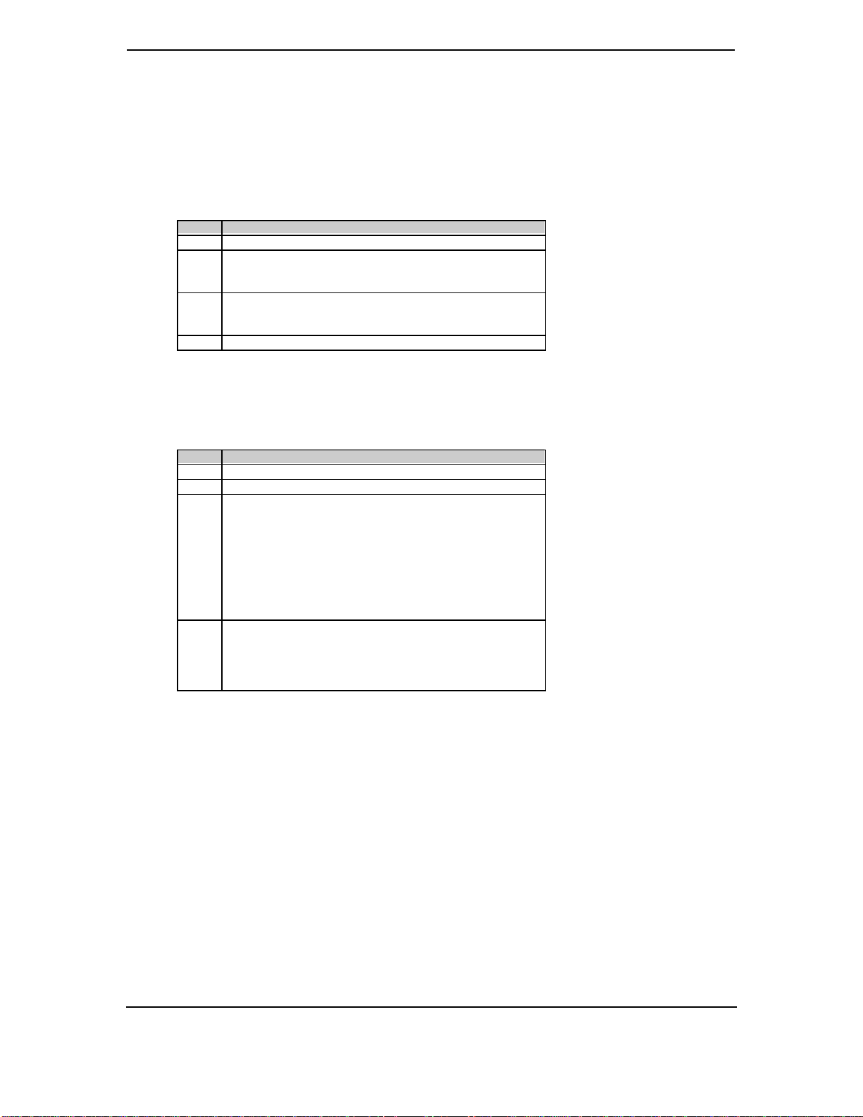
Drive Control Register, I/O Port 3F6h/376h (Write Only)
Bit Function
7..3 Reserved
2 Controller Control:
0 = Re-enable
1 = Reset
1 Interrupt Enable/Disable
0 = Disable interrupts
1 = Enable interrupts
0 Reserved
Drive Access Register, I/O Port 3F7h/377h (Read Only)
Bit Function
7 Res erved
6 WRITE GATE- Signal Active (if set)
5..2 Head Select:
0000 = 15 1000 = 7
0001 = 14 1001 = 6
0010 = 13 1010 = 5
0011 = 12 1011 = 4
0100 = 11 1100 = 3
0101 = 10 1101 = 2
0110 = 9 1110 = 1
0111 = 8 1111 = 0
1,0 Drive Select:
00 = Disabled
01 = Drive 1 selected
10 = Drive 0 selected
11 = Invalid
Technical Reference Guide
Compaq Deskpro 4000N and 4000S Personal Computers
Firs t Edition - September 1997
5-7
Page 98
Chapter 5 Input/Output Interfaces
5.2.2 IDE CONNECTORS
This system includes two standard 40-pi n connectors and one 50-pin connector for IDE devices.
Devices attached to the 40-pin connectors obtain power through a separate connector. The 40-pin
connector is shown in the illustration below followed by the connector’s pinout.
Figure 5–1. 40-Pin IDE Connector.
Table 5–5. 40-Pin IDE Conn ector Pinout
Pin S ignal D escr ipt ion Pin Signal Description
1 RESET- Re set 21 DRQ DMA Request
2 GND Ground 22 GND Ground
3 DD7 Data Bit <7> 23 IOW- I/O Write
4 DD8 Data Bit <8> 24 GND Ground
5 DD6 Data Bit <6> 25 IOR- I/O Read
6 DD9 Data Bit <9> 26 GND Ground
7 DD5 Data Bit <5> 27 IORDY I/O Channel Ready
8 DD10 Data Bit <10> 28 CSEL Cable Select
9 DD4 Data Bit <4> 29 DAK- DMA Acknowledge
10 DD11 Data Bit <11> 30 GND Ground
11 DD3 Data Bit <3> 31 IRQn Interrupt Request [1]
12 DD12 Data Bit <12> 32 IO16- 16-bit I/O
13 DD2 Data Bit <2> 33 DA1 Address 1
14 DD13 Data Bit <13> 34 DSKPDIAG Pass Diagnostics
15 DD1 Data Bit <1> 35 DA0 Address 0
16 DD14 Data Bit <14> 36 DA2 Address 2
17 DD0 Data Bit <0> 37 CS0- Chip Select
18 DD15 Data Bit <15> 38 CS1- Chip Select
19 GND Ground 39 HDACTIVE- Drive Active (front panel LED) [2]
20 -- Key 40 GND Ground
NOTES:
[1] Primary connector wired to IRQ14, secondary connector wired to IRQ15.
[2] Pin 39 is used for spindle sync and drive activity (becomes SPSYNC/DACT-)
when synchronous drive are connected.
Table 5-5.
40-Pin IDE Connector P inout
5-8
Compaq Deskpro 4000N and 4000S Personal Computers
Firs t Edition – Sept ember 1997
Page 99
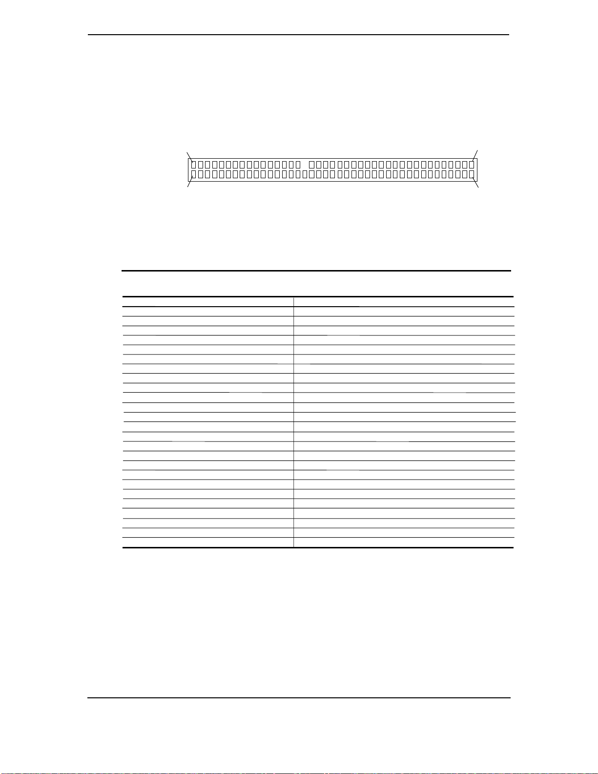
Technical Reference Guide
The 50-pin connector is in ten ded for a CD-ROM drive that operates as a slave on the secondary
IDE interface. This interface includes power and audio signa ls. The 50-pin connector is
illustrated below followed by the pinout.
P2
P1
Figure 5–1. 50-Pin IDE Connector.
Table 5–6. 40-Pin IDE Conn ector Pinout
Table 5-5.
50-Pin IDE Connector P inout
Pin S ignal D escr ipt ion Pin Signal Description
1 RE SDRV- Reset 26 GND Ground
2 GND Ground 27 CHRDY I/O Channel Ready
3 SHD07 Data Bit <7> 28 ALE Cable Select [1]
4 SHD08 Data Bit <8> 29 DAK- DMA Acknowledge
5 SHD06 Data Bit <6> 30 GND Ground
6 SHD09 Data Bit <9> 31 IRQ Interrupt Request [1]
7 SHD05 Data Bit <5> 32 IO16- 16-bit I/O
8 SHD10 Data Bit <10> 33 A1 Address 1
9 SHD04 Data Bit <4> 34 PDIAG- Pass Diagnostics
10 SHD11 Data Bit <11> 35 A0 Address 0
11 SHD03 Data Bit <3> 36 A2 Address 2
12 SHD12 Data Bit <12> 37 CS1FX- Chip Select
13 SHD02 Data Bit <2> 38 CS3FX- Chip Select
14 SHD13 Data Bit <13> 39 DASF- Drive Active
15 SHD01 Data Bit <1> 40 GND Ground
16 SHD14 Data Bit <14> 41 AUD L Left Channel Audio
17 SHD00 Data Bit <0> 42 AUD R Right Channel Audio
18 SHD15 Data Bit <15> 43 AUD R RTN Right Channel Audio Return
19 GND Ground 44 AUD L RTN Left Channel Audio Return
20 -- (Key Space) 45 +5 VDC Motor Power
21 DRQ DMA Request 46 +5 VDC Motor Power
22 GND Ground 47 +5 VDC Motor Power
23 IOW- I/O Write 48 +5 VDC Motor Power
24 GND Ground 49 +5 VDC Log Power
25 IOR- I/O Read 50 +5 VDC Log Power
NOTES:
[1] Pin is left floating to make CD-ROM always slave.
Compaq Deskpro 4000N and 4000S Personal Computers
Firs t Edition - September 1997
5-9
Page 100

Chapter 5 Input/Output Interfaces
5.3 DISKETTE DRIVE INTERFACE
The diskette drive interface supports up to two diskette drives through a stan da rd 34-pin diskette
drive connector. All Deskpro 4000S models include a 3.5 inch 1.44-MB diskette drive installed
as drive A. There is no physical provision for a second drive (B).
The diskette drive interface function is integrat ed in t o the 87307 I/O controller component. The
internal logic of the I/O controller is software-compatible with standard 82077-type logic. The
diskette drive controller has three operational phases in the following order:
♦ Command phase - The controller receives t he command from the system.
♦ Execution phase - The controller carries out the command.
♦ Results phase - Status and results data is read back from the controller to the system.
The Command phase consists of several bytes written in series from the CPU to the data register
(3F5h/375h). The first byte identifies the command and the remaining bytes define the
parameters of the command. The Main Status register (3F4h/374h) provides data flow control
for the diskette drive controller and must be polled between each byte transfer during the
Command phase.
The Execution phase starts as soon as the last byte of the Command phase is received. An
Execution phase may involve the transfer of data to and from the diskette drive, a mechnical
control function of the drive, or an operation that remains internal to the diskette drive controller.
Data transfers (writes or reads) with the diskette drive controller are by DMA, using t he DRQ2
and DACK2- signals for control.
The Results phase consists of the CPU reading a series of status bytes (from the data register
(3F5h/375h)) that indicate the results of the command. Note that some commands do not have a
Result phase, in which case the Execution phase can be followed by a Command phase.
During periods of inactivity, the diskette drive controller is in a non-operation mode known as
the I dle phase.
5-10
Compaq Deskpro 4000N and 4000S Personal Computers
Firs t Edition – Sept ember 1997
 Loading...