

Page 1

picoNode Module
Datasheet and Integration
Specification
Compal Confidential and Proprietary. This document is not to be used, disclosed, or distributed to anyone
without express written consent from Compal. The recipient of this document shall respect the security of this
document and maintain the confidentiality of the information it contains. The master copy of this document is
stored in electronic format, therefore any hard or soft copy used for distribution purposes must be considered as
uncontrolled. Reference should be made to Compal to obtain the latest revision.
Page 2

PicoNode Integration Specification
Contents
1 Overview ........................................................................................................................1
1.1 picoNode .......................................................................................................................... 1
2 DC and AC Characteristics ................................................................................................ 2
2.1 Absolute Maximum Ratings............................................................................................... 2
2.2 Recommended Operating Conditions ................................................................................ 2
3 Electrical Interface ...........................................................................................................5
3.1 Signal Descriptions ........................................................................................................... 7
4 Applications .................................................................................................................. 11
4.1 Powered Operating Mode ............................................................................................... 11
4.2 Battery Operated Mode .................................................................................................. 11
5 SPI Interface and Sequences ........................................................................................... 14
5.1 SPI System Interface Overview ........................................................................................ 14
5.2 SPI Mode and Timing ...................................................................................................... 15
5.3 Host Initialization ............................................................................................................ 15
5.4 Startup (Power On) Sequence ......................................................................................... 15
5.5 Wake Sequence .............................................................................................................. 17
5.6 Host-Driven Reset Sequence ........................................................................................... 19
5.7 Host MRQ Release/picoNode Allowed to Sleep Sequence ................................................. 20
6 Power States ................................................................................................................. 21
6.1 Operating States ............................................................................................................ 21
7 SPI Messaging Protocol .................................................................................................. 23
7.1 Arbitration ...................................................................................................................... 23
7.2 Message Protocol ........................................................................................................... 23
7.3 Host Interface SPI Bus State Machine .............................................................................. 26
7.4 SPI Bus Timing Example .................................................................................................. 27
7.5 Host Message SPI Example .............................................................................................. 28
7.6 Host Message “Connect” SPI Example ............................................................................. 30
8 picoNode Provisioning ................................................................................................... 33
9 Antenna Diversity .......................................................................................................... 34
9.1 Antenna Design Considerations ....................................................................................... 34
ii
Page 3

PicoNode Integration Specification Contents
9.2 Diversity Considerations ................................................................................................. 35
9.3 Block Diagram ................................................................................................................ 36
9.4 Antennas ....................................................................................................................... 36
10 Regulatory Considerations ............................................................................................ 39
10.1 FCC Warnings ............................................................................................................... 39
11 Errata .......................................................................................................................... 41
Figures
Figure 1 Typical Application Diagram ...................................................................................... 1
Figure 2 SPI Timing, CPOL = 0, CPHA = 0 .............................................................................. 15
Figure 3 picoNode Power-up Timing Sequence ...................................................................... 16
Figure 4 Host-Initiated picoNode Wake Sequence – SRDY Low (Synchronous) ...................... 17
Figure 5 Host-Initiated picoNode Wake Sequence – SRDY High (Asynchronous) .................... 18
Figure 6 Host-Driven Reset Sequence................................................................................... 19
Figure 7 Host MRQ Release/picoNode Allowed to Sleep Sequence ........................................ 20
Figure 8 SPI Master and Slave Message Sequences ............................................................... 25
Figure 9 Host Interface SPI Bus State Machine ...................................................................... 26
Figure 10 SPI Timing Example .............................................................................................. 27
Figure 11 Host Message on SPI – MMsg Pair ......................................................................... 28
Figure 12 Host Message on SPI – MHdr Pair .......................................................................... 29
Figure 13. Antenna Diversity with Ethertronics ...................................................................... 34
Figure 14 picoNode Block Diagram ....................................................................................... 36
Figure 15 Controlled Impedance RF Trace Design .................................................................. 38
Figure 16 picoNode PCB Land Pattern .................................................................................. 45
Figure 17 picoNode PCB Land Pattern Keepouts ................................................................... 45
Figure 18. Powered Example ................................................................................................. 46
Figure 19 Lithium Battery Example ...................................................................................... 46
Figure 20 picoNode Mechanical Dimensions.......................................................................... 47
iii
Page 4

PicoNode Integration Specification Contents
Tables
Table 1. picoNode Specifications ............................................................................................ 1
Table 2. Absolute Maximum Ratings ....................................................................................... 2
Table 3. Operating Conditions ................................................................................................ 2
Table 4. Operating Characteristics .......................................................................................... 2
Table 5. picoNode Pin Descriptions ......................................................................................... 5
iv
Page 5

PicoNode Integration Specification
Revision History
Revision Release Date Change Description
0.1 May 10, 2017 Initial release
0.2 Jan. 15, 2018 Update Tables 1 and 4
0.3 Jan. 31, 2018 Add FCC Warnings in Sec. 10
v
Page 6
PicoNode Integration Specification
1 Overview
This document provides a brief overview of guidelines allowing an integrator to design a Host
product that utilizes the picoNode and ensures that the system meets all of its technical
objectives and requirements.
1.1 picoNode
The picoNode is a small form factor wireless network module that easily integrates with a
microcontroller or applications processor using a Serial Peripheral Interface (SPI). The top side
of the printed circuit board (PCB) is enclosed with a radio frequency (RF) shield. The picoNode is
an LGA-style module designed to be soldered directly onto a host board via SMT processes. For
details, see Appendix B: PCB Land Pattern and Keep-outs.
Table 1 picoNode Specifications
picoNode
Dimensions (per unit) 26 mm x 16 mm
Thickness: 2.4mm
Weight (per unit) 1.5 Grams
Transmit Power 21.5 dBm (typical)
RX Sensitivity -133 dBm (nominal)
For more mechanical details about the picoNode, refer to the mechanical drawing in 0D
Appendix D picoNode Mechanical Drawing.
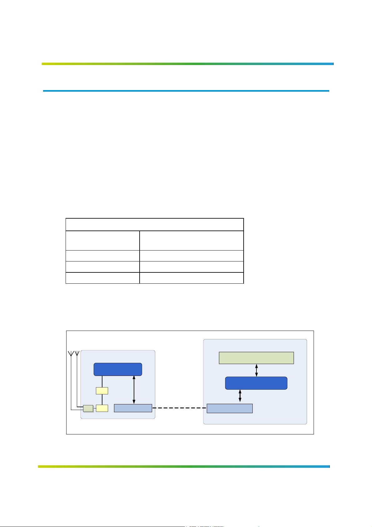
The following figure shows how a picoNode interfaces with a Host application, running on an
applications processor.
Host
Sensor or Meter Reading or
Location Tracking Appl ication
Host Interface Protocol
Application
SPI Master Driver
MAC
RF PHY
Node
Host Interface
SPI Slave Driver
Figure 1 Typical Application Diagram
1
Page 7

PicoNode Integration Specification
2 DC and AC Characteristics
2.1 Absolute Maximum Ratings
Operating outside of these ranges may damage the unit.
The picoNode is MSL 3-rated and should be handled as an MSL 3 device per IPC/JEDEC J-STD033 (latest revision).
Table 2 Absolute Maximum Ratings
Parameter Min Max Unit
Storage Temperature -40 85 ⁰C
Operating Temperature -40 85 ⁰C
Vbatt Input Voltage 2.5 6.0 V
3.3V Supply 3.1 3.5 V
Digital Interface Signals, 3.3V nominal 3.0 3.6 V
2.2 Recommended Operating Conditions
Table 3 Operating Conditions
Parameter Min Max Unit
Input voltage, VBATT 2.5 5.5 V
3.3V Input 3.2 3.4 V
Ambient Temperature, Ta -40 85 ⁰C
The following characteristics apply across the -40°C to +85°C temperature range unless
otherwise noted.
Table 4 Operating Characteristics
Description Min Typ Max Units
DC Characteristics
Voltage – Vbatt 2.5 3.3 5.5 Volt
Off Current – Note 1 0.1 µA
Deep Sleep Current - Note 1 19 µA
Idle Current – Note 1 20 mA
Receive Current – Note 1 100 mA
picoNode: Transmit Current – Note 2 330 mA
2
Page 8

PicoNode Integration Specification
Description Min Typ Max Units
Digital
VOL – Voltage Output, Low (4mA sink) 0 0.4 V
VOH – Voltage Output High (4mA source) 2.4 3.3 V
SPI Clock – Note 11 0.1 8.6 MHz
Environmental
Operating Temperature -40 +85
Storage Temp -40 +85
Humidity – non-condensing 5 95 %
Ramp Temperature (maximum rate at which operating
temperature should change)
MTBF (picoNode) MHrs
Receiver
Receiver Sensitivity – Note 3 -133 dBm
Receiver Image Reject 25 33 dB
Noise Figure 4.9 dB
Input IP3 (high LNA gain mode) dBm
Maximum RF input level for specification compliance dBm
General RF Characteristics
Frequency Range – Note 4 2402 ~2482 MHz
Channel Spacing N/A 1.99 N/A MHz
Transmitter
Maximum RF Conducted Power –Note 5
FCC/IC markets:
ETSI markets:
Carrier Rejection -35 -51 dBc
Signal Modulation DSSS-
Signal Bandwidth 1.0 MHz
BT Factor 0.3
Peak to Average Ratio 2.3 dB
Spectral bandwidth at maximum RF power:
-6dB BW
-20dB BW
ACPR – Note 6 -30 dBc
Harmonics – Note 7 -43 dBm
Transmit Power Level Accuracy – Note 8
30
8.5
21.5
9.5
DBPSK
0.96
1.75
23.65
10
±1.5
°C
°C
°C/Hr.
dBm
dBm
MHz
MHz
dB
3
Page 9

PicoNode Integration Specification
Description Min Typ Max Units
Transmitter Spurious Outputs – Note 9
30MHz to 2400MHz:
2482MHz to 8000MHz:
VSWR Tolerance
Maximum VSWR for spec compliance – Note 10:
Maximum VSWR for stability.
< -43
< -43
1.5:1
9:1
dBm
dBm
NOTES:
1. Tested at 3.3V input, +25C. Please note the following:
a. There are power differences between the Voltage/Current numbers in this table.
b. The Table 4 refers to a maximal current draw that the Host system should be designed
to accommodate.
2. Measured at:
picoNode: +21.5 dBm TX output (Typ=50Ω), 3.3 V, range includes VSWR ≤ 1.5:1 (Po not
compensated).
3. Sensitivity at maximum DL spreading factor of 11 (2048) with 10% FER.
4. The upper frequency range is market dependent:
c. FCC/ISED: CH38; 2475.63 MHz.
d. ETSI: CH40; 2475.63 Hz.
e. Japan: CH41; 2481.60 MHz.
5. Maximum TX RF power:
picoNode: This is limited by FCC/IC grant to 21.5 dBm in these markets. Transmit power is
configured during network join time to meet country-specific deployment and regulatory
requirements. The configurable range is 0 – 21.5 dBm in 1 dB integer increments. For noninteger Power such as 21.5dBm, the Node’s MAX_TX Power must be set to 22dBm to force a
maximum calibrated value.
6. Spec and test method comes from FCC 15.247(d); Band Edge Emissions, 2 MHz offset.
7. At any TX power level, VSWR ≤ 3:1. Harmonics fall into FCC restricted bands.
8. Estimated sum of all contributors with VSWR ≤ 1.5:1. Normal link mode.
9. At any TX power level, VSWR ≤ 3:1. Applies to spurious, not ACPR or harmonics. Generally
the largest spurious output outside the 2.40-2.48GHz band is at 2/3LO and 4/3LO.
10. Maximum VSWR for spec compliance applies at 25°C only. Slightly degraded ACPR/mask
and power variation can be expected at temperature extremes.
11. The SPI clock has a maximum rate of 26 MHz/3 and a minimum of 100 kHz. There is no
physical limitation on the minimum clock rate but the 100 kHz is deemed “marginal” and is
not absolute. Depending on the data traffic model and level of debug traffic, 100 kHz may
cause a backup of SPI traffic, which then causes buffer overflow conditions. The application
must be validated to ensure that the SPI clock is sufficient to support required traffic.
4
Page 10

PicoNode Integration Specification
3 Electrical Interface
This chapter describes the electrical interface of the picoNode and how the Host processor controls for
the picoNode.
Table 5 picoNode Pin Descriptions
Pin # Pin Name Signal Direction
Relative to picoNode
2 WAKE Output, 1.8V CMOS_O* This is a 1.8V output signal that
1,3,4,5,7,10,12,
14,18,24,26,28,
29,30,31,32,34
23 3V3 Power Power The 3.3V can be continuously
15 VBATT Power Power Input power to the picoNode. This
Ground Power Power Ground return. Should be low RF
Signal Type Comment
reflects the status of the Node’s
power state. When WAKE is “high”
the Node is active in Idle, RX, or TX
states. When WAKE is “low”, the
Node’s 3.3V is internally gated OFF
and the Node is in its lowest power
state. This signal is to be used for
“battery operating modes”, as
describe in Figure 6 Lithium Battery
Example.
Connect the WAKE pin directly to
the enable pin of a voltage regulator
or FET switch controlling 3.3V
impedance to a solid ground plane
of the Host
supplied(line powered) or only when
the WAKE pin is asserted
“high”(battery powered). This
power domain is high power
(internal CPU, Transceiver, and RF
PA) and should be decoupled with a
low ESR, high capacitance
Capacitor.
power domain is low current but is
used 100% of the time to supply
internal Supervisory domains.
5
Page 11

PicoNode Integration Specification
Pin # Pin Name Signal Direction
Signal Type Comment
Relative to picoNode
8 SRQ Output CMOS_O SPI Slave Request. SRQ must be
connected to a pin that can wake
the application processor from
sleep, for battery powered
applications.
9 SRDY Output CMOS_O SPI Slave Ready
21 SCLK Input CMOS_I SPI Clock
19 MISO Output CMOS_O SPI Master Input Slave Output
22 CS Input CMOS_I SPI Chip Select(Note other slaves
are prohibited on the SPI interface,
but this pin must be controlled by
the Host Common Library). It
CANNOT be tied low on the PCB.
20 MOSI Input CMOS_I SPI Master Output Slave Input
11 MRQ Input CMOS_I SPI Master Request
13 ON_OFF Input CMOS_A This is used to turn ON/OFF the
Internal Power supplies of the
picoNode. It is controlled by the
Host Common Library.
Low: Node consumes <1uA
High: Node is active and will run
through a wide range of power
states.
17 TOUT Output CMOS_O TOUT is a normally low signal that
pulses high in response to specific
Network Timing Events. It allows an
application to trigger a
measurement with sub-1ms
accuracy.
6 RF_TXENA Output CMOS_O This signal is used to indicate status
of the Power Amplifier for the
picoNode:
Low = OFF
High = Enabled (Transmitting)
The rise edge can be used to trigger
a Host CPU’s ADC read of VBATT
(battery voltage while under
maximum load).
6
Page 12

PicoNode Integration Specification
Pin # Pin Name Signal Direction
Relative to picoNode
25,
27
33 RF_SHDN Output CMOS_O This pin indicates the status of the
16 TIME_QUAL Output CMOS_O This pin is reserved and should be
RF1,
RF2
RF RX/TX 50 Ohm These are the RF ports for the
Signal Type Comment
picoNode. They are 50 Ohm port,
DC coupled. RF1 is required but both
are desired for antenna diversity.
Single port or dual antenna port can
be configured in the provisioning
process.
RF Transceiver for the picoNode:
Low = Shutdown
High = Active
It can be used for WIFI/BT
coexistence, and to reduce power
supply current during low power
states (see 3.1.3)
left as Do Not Connect.
NOTES:
1. The VDD of the internal logic of the picoNode is 3.3Volt.
2. The Host is the SPI Master and the picoNode is the SPI Slave.
3. CMOS_I: The Node input voltages are 3.3V CMOS levels. VIH = 2.0V (minimum) and
VIL = 0.8V (maximum).
4. CMOS_O: The Node output voltages are 3.3V CMOS levels (4mA). VOH = 2.4V (minimum)
and VOL = 0.4V (maximum).
5. SPI inputs to the node (SCLK, MOSI, CS) must be tri-stated or driven low when the node
may be sleeping (MRQ and SRQ are both low). See section 5: SPI Interface and Sequences
for more details.
3.1 Signal Descriptions
3.1.1 GND
Ground is the Host CPU’s ground to enable a common reference between CPU and Node.
3.1.2 VBATT
This supplies a low current 2.5 V – 5.5 V for the Node’s internal supervisory circuitry. This pin
should be decoupled with a 0.1 µF capacitor on the Host processor board.
7
Page 13

PicoNode Integration Specification
3.1.3 3V3
This pin drives the CPU, Transceiver, RF PA section of the module. It can consume up to 800 mW.
Allow for bypassing with a 47 µF low ESR cap (bulk) and a 0.1 µF ceramic cap for optimal
performance. Depending on the Host design, there are some nuances that are important
regarding this signal:
3.3 V can be supplied continuously or only when the WAKE signal is asserted “high.”, for
battery powered applications.
The Node runs through various operating states when 3.3V is supplied.
If the Node internally is in a state that requires no RF, the 3.3 V can be “noisy” (+/-100
mV ripple). The RF state is defined by the RF_SHDN pin. This allows the Host’s 3.3 V
regulator to work in low quiescent (power save) modes.
If the Node internally is active and does require RF, the 3.3 V must be “clean” (+/-20mV
ripple). This forces the Host’s 3.3V supply into a high precision mode and forcing a high
quiescent current of that regulator.
If the Node is operated in a battery mode, when 3V3 isn't always enabled, the 3V3
supply must power up and be stable within 2mS of the WAKE signal going "high"
This switching of “noisy” and “clean” becomes clear (and important) when working with battery
operated devices and optimal low power drain.
3.1.4 ON_OFF
This input signal controls the power-on of the LDO circuitry for the picoNode. This signal is
controlled by the Host Common Library, compiled onto the user’s apps processor. For reference
only: It must be shut off prior to starting the picoNode power-up sequence as defined in section
5.4: Startup (Power On) Sequence. After the picoNode powers up, this signal is to remain logic
high during normal operational modes. This pin dually serves a power on/off function as well as
a Node Reset function.
3.1.5 MRQ
The MRQ (Master Request) is the Host’s normal way of waking the picoNode to initiate SPI
communications. Logic “High” forces the picoNode awake. This signal is controlled by the Host
Common Library, compiled onto the user’s application processor.
3.1.6 SRDY
SRDY (Slave Ready) is an indication from the picoNode that it has fully booted its internal
Firmware image, initialized its Hardware and Interfaces, and is ready for communication
(arbitration) with the Host. Logic “High” indicates the picoNode is ready for communications.
This signal is controlled/handled by the Host Common Library, compiled onto the user’s
application processor.
8
Page 14

PicoNode Integration Specification
3.1.7 SRQ
The SRQ (Slave Request) signal is an indication from the picoNode that it wants the Host’s
attention. When SRQ is asserted “High,” the Host must read the Status registers of picoNode. If
SRQ is “High,” SRDY will also be “High.” This signal is controlled/handled by the Host Common
Library, compiled onto the user’s application processor.
For battery powered applications, SRQ must be connected to a pin that can wake the
application processor from sleep.
3.1.8 SPI System
The SPI system is the generic term used for all SPI signals (MOSI, MISO, CS, SCLK) to be set up
for SPI communications to occur between Host and picoNode. The picoNode SPI is the Slave in
the Master/Slave communications and is defined in section 5.2: SPI Mode and Timing.
IMPORTANT NOTES:
1. Other SPI slaves are not allowed to share the SPI signals.
2. CS must be controlled by the Host Common Library API to guarantee correct sequencing.
Specifically, the user must ensure that the SPI CS is active (low) for the whole duration of a
message transfer, with no gaps.
3.1.9 TOUT
This signal is a Time Synchronizing signal that pulses high upon specific network timing events.
3.1.10 RF_TXENA
This signal indicates when the device is transmitting. When transmitting, it is recommended
that the Host processor use this opportunity as a trigger to read the system “Vbatt” power line
to show battery voltage under maximum load.
3.1.11 RF_SHDN
This Node signal indicates status of the RF Transceiver of the picoNode. If low, the transceiver
sleeps (no RX and no TX). This output of the module (3.3 V) indicates when the RF transceiver is
on or off. When RF_SHDN is high, the RF is “ON” (RX or TX). In the RF “ON” mode, the module
needs a “clean” 3.3 V (low ripple).
3.1.12 RF1 and RF2
These are the RF ports (RX and TX) of the Node. They are DC-coupled, 50 Ohm and require
special Host routing of PCB. RF1 is the primary antenna and is always required. RF2 is a
secondary antenna that the Node can use for Antenna Diversity. A single or dual antenna
(diversity) system can be configured during the Provisioning process. For best results ensure
the load termination (antenna) has a VSWR of 1.5:1 or better (return loss < -10 dB).
9
Page 15

PicoNode Integration Specification
3.1.13 WAKE
The WAKE signal is generated by the module and is 1.8V. It signals that it now requires a 3.3V
source. Generally, for a Powered Node (Figure 5 Powered Example) the WAKE is not required
since 3.3V already exists. In the battery example (Figure 6 Lithium Battery Example) the WAKE
turns on the Host's main supply to regulate the battery to the required 3.3V.
If WAKE is used to enable the Host's 3V3 supply, the 3V3 supply must be on and stable within
2mS of WAKE going high.
3.1.14 TIME_QUAL
This signal is reserved for Compal.
10
Page 16

PicoNode Integration Specification
4 Applications
This chapter describes two major methods of implementing the picoNode: Powered and
battery operated modes.
1. Powered Operating Mode
“Powered” refers to the Host board and its power supply. Specifically, it refers to a good
solid, consistent power supply – such as an AC powered source. In this type of usage case,
the Host can potentially supply a good clean 3.3 V rail (pin 4) without regard to extreme
detail of optimizing power consumption.
2. Battery Operated Mode
This mode refers to a battery operated device in which extreme care and attention is
applied to reducing overall power consumption. All details and all modes of power
consumption are considered and optimized.
4.1 Powered Operating Mode
In this scenario, the Host and Node’s power consumption is not really a consideration. In this
case, the Host can take an input Voltage and convert to a 100% duty 3.3 V supply. This would be
applied to:
Host CPU
VBATT of picoNode
3V3 of picoNode
In this case, the node will internally turn the 3.3 V rail ON/OFF as it is required. The Node
attempts to gate this internal supply OFF to conserve power, when it can. The HW status of the
3.3V supply is the WAKE signal (3.3V = “ON” if WAKE is High). When the 3.3V is internally gated
off, the Node consumes virtually no power on that supply.
However, the Host CPU is always powered by 3.3 V – the operating level of the Host-picoNode
SPI interface. The picoNode requires a full 3.3 V during SPI transfers. For a wired example of the
Powered circuitry, refer to Figure 5 Powered Example.
4.2 Battery Operated Mode
Battery operating mode offers a much more challenging design constraint. The goal is to
reduce current consumption where possible. To this conservation goal, see Figure 6 Lithium
Battery Example.
The assumption in this design goal is to use a long life battery such as Lithium battery/cell.
These primary cells offer:
Extreme low self-discharge
Long life
11
Page 17

PicoNode Integration Specification
Wide operating temperatures
High capacity
2.5 V – 3.6 V direct voltage over the operating temperature and discharge
characteristics of the cell
In this case, assume that:
The VBATT pin of the Node is connected directly to the cell (2.5 V – 3.6 V).
The 3V3 signal of the Node is connected directly to the 3.3 V regulator. The regulator is
turned ON/OFF depending on the state of the WAKE pin of the Node.
The CPU uses an indirect path through a dual Schottky diode to permit seamless
switching/transition from battery voltage to 3.3 V.
Most modern CPUs used for this type of application have the following characteristics:
Operate at 1.8 V – 3.6 V
Low sleep current (1 – 2 µA with full SRAM retention for fast wakeup)
Pins that use interrupts to wake the processor from deep sleep
The following sections describe the major operating states and power supply modes.
4.2.1 Sleep Mode Assumptions
1. The Node is powered “on” (ON_OFF = high).
2. The Node is in sleep mode when in the WAKE state (WAKE = low).
3. The Node is consuming minimal current through its VBATT pin.
4. 3V3 is off and is not required by the Host or Node.
5. The Host CPU can run off the “natural voltage” of the cell only drawing microAmps of
current.
4.2.2 Active Mode
When the Node awakens (WAKE = high) and the 3.3 V power supply is turned “on”:
The Node uses the supplied 3.3 V as required. The 3V3 must be on and stable within 2mS of
WAKE being asserted high.
The voltage of the CPU ramps to the higher of the following: cell voltage or 3.3 V supply.
The 3.3 V on the Host and the Node permits the Node to fully function on the RPMA
network and also allows Host-Node SPI communications.
A Texas Instruments TPS63000 3.3 V buck/boost regulator (or equivalent) is recommended for
picoNode applications. This has some unique benefits:
When in high efficiency mode (PS/SYNC = low), the regulator outputs a loose 3.3 V with
+/-100 mV ripple. In this mode, its quiescent current is only 50 µA.
When in low efficiency (but “clean” output) mode (PS/SYNC = high), the regulator is within
+/-20 mV ripple but consumes a 0.6 mA quiescent current.
12
Page 18

PicoNode Integration Specification
These operating modes align well with the Node’s operating modes as defined by the
RF_SHDN pin:
When tight regulation (low ripple) is required by the RF of the Node:
RF_SHDN = high
PS/SYNC = high
When the Node does not need tight regulation and is in a moderately low power mode,
RF_SHDN is low (and PS/SYNC is low).
Other design considerations for optimal low power are as follows:
1. Reduce capacitance in the 3.3V domain. Extra capacitors require charging each time the 3.3
V is turned "on".
2. Ensure all software and CPU configurations set CPU pins to low power states.
3. Use high value resistors such as 1 M or greater for pull-ups/pull-downs where possible.
13
Page 19

PicoNode Integration Specification
5 SPI Interface and Sequences
5.1 SPI System Interface Overview
The SPI slave interface is currently the only supported interface for Host-to-Node communication.
The SPI System interface is controlled/handled by the Host Common Library, compiled onto the
user’s apps processor. The following section (all of section 5) is informational only.
NOTE: The picoNode must be the only SPI slave on the bus.
The SPI slave interface provides communication with an external Host through a 7-wire interface.
The Host is the SPI master and the picoNode is the SPI slave. In addition to the four standard SPI
signals, three additional signals are used to complement the SPI bus: MRQ, SRQ, and SRDY. The
additional signals are included to support picoNode state transitions and bi-directional message
traffic.
The SPI signals include four that are controlled by the master and three that are controlled by the
slave.
Master-controlled Signals (Host) Slave-controlled Signals (picoNode)
MOSI
SCLK
CS
MRQ
MISO
SRQ
SRDY
When MRQ and SRQ are low, the remaining Master controlled signals (MOSI, SCLK, and CS)
must be held low or tri-stated. This is to prevent these signals from back-driving the picoNode
(Slave) that may be in deep sleep. When either MRQ or SRQ assert high, the Master should set
each of the three signals appropriately according to their standard usage. No pull-up resistors
should ever be applied to any signals on the picoNode since it often needs to fall into a Deep
Sleep mode (all internal regulators turned off).
MISO
MOSI
SCLK
CS
MRQ
SRDY
SRQ
ON_OFF
T_OUT
3V3/VBATT
GND
RF1
RF2
Radio
Node
Analog
Front End
ARM7 +
Digital
Processing
RTC
SPI
Interface
Ingenuspecific
SPI
14
Page 20

PicoNode Integration Specification
5.2 SPI Mode and Timing
SPCK Cycle
(for refere nce)
SPCK
(CPOL = 0)
1
2 3 4 5 6 7 8
MOSI
(from master)
MISO
(from slave)
NSS
(to slave
)
MSB
MSB
5.3 Host Initialization
What is described here is the initialization of the Host, its operating software, and the control
sequences used to drive the picoNode.
Due to specific clock and memory requirements, the picoNode must go through specific
Initialization and Wake sequences.
NOTE: Some CPUs have internal pull-up resistors that are active after Power On Reset. Through
CMOS leakage, the Host CPU can supply voltages to the picoNode I/O bus prior to the
Host CPU fully initializing and disabling the pull-up resistors. It must be noted that during
the brief initialization period, the ON_OFF signal must be “low.” Activating the ON_OFF
signal with other picoNode signals being pulled “high” can cause CMOS latchup within
the picoNode.
6 5 4 3 2 1
6 5 4 3 2 1
Figure 2 SPI Timing, CPOL = 0, CPHA = 0
LSB
LSB
*
5.4 Startup (Power On) Sequence
During, and immediately after Power On Reset (POR), the Host has no control of its I/O power
states. For instance, some CPUs have GPIO that tri-state or act as inputs during power up. Other
CPU brands have programmable pull-ups on its I/O and need the Host CPU to disable those pullups for the Host’s GPIO to work correctly with the picoNode. This setup and configuration of
GPIO takes a finite time during the Host boot process. This is detailed in the following figure.
Whereas the power-up sequence is described here, it is recommended the Integrator not attempt
this entire startup sequence without assistance. Compal offers a formal and controlled library to
help with this startup and communication interface.
The initial sequencing of the 3.3V and Vbatt rails are:
• Both 3.3V and Vbatt van be applied simultaneously, or
15
Page 21

PicoNode Integration Specification
• The Vbatt can rise first if 3.3V follows within 1mS, but
• the 3.3V should never rise prior to Vbatt.
3.3V/V
BATT
Host Init
(not a signal)
Power On
Int Node
Reset /Init
(not a signal)
MRQ
t
1
Hi-Z
100 ms
3000 ms 10 ms 4 ms
t
t
2
3
t
t
t
4
5
t6– t4< 300 ms or error
6
SPI
System
SRDY
t
0
Figure 3 picoNode Power-up Timing Sequence
The timing sequence shown in Figure above is described below. NOTE: The timing shown in the
figure is not to scale.
t0 t1
This phase is where the Host’s System power has been applied and the Host
Software must power up and initialize the GPIO interfaces for the picoNode to
the required states defined at time t1. The t1 state becomes “TRUE” indicating
the Host sets all the GPIO to a known and controlled state (Low).
t2
At t2 state, all the output signals to the picoNode are set low and the Power On
Signal is set high. This turns on the internal LDO regulators of the picoNode to
initiate a power up sequence. The time between t1-t2 is approximately 100 ms, or
longer. Assert ON_OFF “high” starts an internal clock (32 K) and releases an
internal reset pin which may take up to 3 seconds to stabilize.
t3
t3 is when the Host releases the picoNode from its Reset state. This time allows
the 32 kHz of the picoNode to turn on and stabilize. The time between t2-t3 is 1
second, or longer.
t4
t4 signals the start of the Host wanting to initiate communications (arbitration)
with the picoNode. The Host raises MRQ to turn on various circuitries. The time
between t3-t4 is 10 ms, or longer.
t5
After the assertion of t4, the picoNode begins its “wake sequence.” The picoNode
must boot, initialize its operating system and hardware and when it is ready for
16
Page 22

PicoNode Integration Specification
communications it raises its SRDY signal back to the Host. At this point,
communications (Arbitration) can begin.
t6
At this point the picoNode signals its readiness by asserting the SRDY pin. The
Host can now begin communications with the picoNode.
5.5 Wake Sequence
The picoNode will often go into sleep mode even though ON_OFF is “high” (active). To begin
Node-Host communications, the host must ensure the picoNode is awake. The picoNode can be
awakened in two manners:
MRQ assertion from the Host. The Host desires communications with the picoNode and
awakens the picoNode by asserting the MRQ line. This is a Synchronous Wake Sequence.
The picoNode can “self-awaken” due to network events. In this case, a timer internal to the
picoNode “pops” and triggers the picoNode to “wake.” When the picoNode is awake it asserts
its SRDY as a matter of course to indicate to the Host (if it needs to) that it can start
communicating with the picoNode while it is awake. This is an Asynchronous Wake Sequence.
5.5.1 Wake Sequence (Synchronous)
The following sequence demonstrates the timing required of the Host to awaken the picoNode
from a sleep state.
Assumptions:
The picoNode has been previously Powered On and Arbitrated.
The power (VBATT) has remained stable and the picoNode has not been Reset (Reset is set to
tri-state/float).
MRQ
SPI
Hi-Z
(Driven as appropriate)
System
SRDY
3 ms
t
0
4 ms
t
1
t
2
t
3
Figure 4 Host-Initiated picoNode Wake Sequence – SRDY Low (Synchronous)
17
Page 23

PicoNode Integration Specification
The timing sequence shown in Figure 4 Host-Initiated picoNode Wake Sequence – SRDY Low
(Synchronous). NOTE: The timing shown in the figure is not to scale.
t0
The Host desires to wake the picoNode and asserts MRQ high.
t0 t1
After MRQ has gone High, the Host’s SPI system and other I/O can be enabled.
Asserting the MRQ has enabled the internal I/O power supply of the picoNode
and the Host’s SPI can be enabled 4 ms after the rise of MRQ.
t1 t2
After the initial assertion of MRQ, the picoNode has to internally power up and
initialize its systems. When it is ready to communicate it will assert its SRDY line
to signal it is now ready for SPI interaction. From MRQ assertion until the
picoNode is ready, takes about 80 ms.
t2
The picoNode is now ready to fully communicate with the Host.
5.5.2 Wake Sequence (Asynchronous)
In this scenario, the picoNode is already awake due to a networking event (SRDY is already High)
and the Host wants to communicate with the picoNode while it is awake. The Host asserts MRQ
to ensure that the picoNode stays awake during its communication cycle.
NOTE: The timing shown in the figure is not to scale.
MRQ
SPI
System
SRDY
Hi-Z
< 250 μs
t
0
t
(Driven as appropriate)
1
t
2
Figure 5 Host-Initiated picoNode Wake Sequence – SRDY High (Asynchronous)
18
Page 24

PicoNode Integration Specification
5.6 Host-Driven Reset Sequence
If the picoNode fails to communicate (or similar), it may be necessary to “Reset” the picoNode.
The following figure shows the proper sequence to reset the device.
NOTE 1: Resetting the device causes it to go through an RPMA Cold Acquisition process to
reacquire the network.
NOTE 2: The timing shown in the figure is not to scale.
V
BATT
ON_OFF
MRQ
SPI
System
SRDY
Hi-Z
15 ms
t
0
t
1
3000 ms 10 ms 4 ms
t
2
t
3
t
4
(Driven as appropriate)
t
5
t
6
Figure 6 Host-Driven Reset Sequence
19
Page 25

PicoNode Integration Specification
5.7 Host MRQ Release/picoNode Allowed to Sleep Sequence
If the Host determines there are no more messages or SPI transactions required, it nominally deasserts the MRQ to allow the picoNode to fall back to Deep Sleep (lowest power mode). The
figure below shows how this is sequenced by the Host/picoNode. A small delay in de-asserting
SRDY is enforced to prevent quick toggling (waking) of the picoNode.
NOTE: The timing shown in the figure is not to scale.
MRQ
SPI
System
SRDY
Hi-Z
10 ms3 ms
t
0
t
1
t
2
Figure 7 Host MRQ Release/picoNode Allowed to Sleep Sequence
20
Page 26

PicoNode Integration Specification
6 Power States
Compal can provide partners with tools to accurately predict battery life for their particular
application. We recommend that partners use these tools. This section is provided for reference
only.
The picoNode has a number of states it runs through during its various operating modes.
General comments:
The picoNode accepts a wide input voltage range (2.5 V – 5.5 V on VBATT).
The picoNode has low drop out (LDO) regulators that will operate 100% of the time the
picoNode is powered (ON_OFF signal set to high).
The picoNode requires either a fixed or switched 3.3 V supply on its 3V3 pin.
The picoNode always tries to minimize its power consumption but is largely driven by network
operating states and modes of operation. This document does not describe all of the modes in
detail but, in general, there are two main operating modes for the picoNode:
1. Continuous Mode
In this mode, the picoNode is ON (awake) at least 50% of the time (100% of its RX cycle).
The picoNode starts up, searches for the network, locks on, and Joins. In this mode, the
picoNode is nominally in RX or TX mode (radio is ON and in a high power consumption
state), or in an Idle state where the clocks and CPU are ON but the radio is OFF (moderately
low power mode). The continuous mode is usually for applications where the Host and
picoNode are AC-powered and system current consumption is not an issue.
2. Slotted Mode
This mode has the picoNode falling into a Deep Sleep state—the lowest power state of the
picoNode. In this mode, the picoNode is mostly powered down except for a couple of low
power LDO Regulators. The picoNode can sleep for hours at a time if the network is
configured to allow this.
The power states are described in the following sections.
6.1 Operating States
This section describes the various operating states within the operational modes.
6.1.1 Power Off State
When the picoNode is totally non-functional, the Host can set the ON_OFF signal Low to
deactivate the circuitry of the picoNode. This should NOT be confused with Deep Sleep states
where the picoNode mostly sleeps yet maintains key network timers to wake up synchronously
with network activity. If awakened from the Power Off state, the picoNode must go through a
very power-hungry search/acquisition algorithm to re-acquire the RPMA Network.
21
Page 27

PicoNode Integration Specification
6.1.2 Deep Sleep State
The picoNode shuts off all its power regulators except a couple low quiescent LDO regulators.
These regulators keep a minimal amount of circuitry alive for tracking network timers, enable a
32 kHz clock, and some minor interface circuitry.
6.1.3 Oscillator Calibration State
When the picoNode is in Deep Sleep state, it attempts to maintain accuracy of its low power 32
kHz clock to enable faster network synchronizing when it wakes up. The CPU of the picoNode is
not activated during this calibration state. The picoNode will periodically (and briefly) wake up
in a very low power mode to calibrate its 32 kHz clock to its very accurate 26 MHz clock. This is
especially important when the temperature varies substantially causing the 32 kHz oscillator to
drift.
This plot is an example of the picoNode performing a self-calibration of its 32 kHz oscillator.
The pulses represent the TCXO being turned on periodically to perform the calibration. The
picoNode wakes itself from Deep Sleep, Calibrates, and then falls back to sleep. Minimal power
is consumed during this self-calibration process. As can be seen, the picoNode does this
approximately every 900 seconds.
6.1.4 Idle State
Idle state has various sub-states but generally refers to a state where the picoNode is “awake”
and its system clock is on, the CPU is awake, but the RF is OFF.
6.1.5 RX State
The picoNode turns on all its clocks, the main CPU and the RF in an RX-only state. The RF
transceiver, in RX state, consumes a moderate amount of power.
6.1.6 TX State
When the picoNode transmits, it uses a variable transmit power that is correlated to its received
RSSI. In this state, the picoNode is likely at its highest power states, but this is somewhat
dependent on RSSI. This is at approximately 23 dBm output power. This is the highest power
state for the picoNode.
22
Page 28

PicoNode Integration Specification
7 SPI Messaging Protocol
The SPI Messaging between the Host processor and the node is controlled/handled by the Host
Common Library, compiled onto the user’s apps processor. The following section (all of
Chapter 7) is informational only.
The details of Host/Node messaging are typically not necessary for integrators to implement.
7.1 Arbitration
Arbitration is the process a Host uses to signal to the Node that it supports the bi-directional
messaging protocol. The arbitration sequence is designed to reduce the probability that an
arbitrary non-Host transfer sequence can mirror a valid arbitration sequence.
Arbitration consists of both Host and Node transmitting an arbitration request/reply pair. After
a defined turn-around delay, both transmit a validation request/reply. The turn-around delay
avoids race conditions between Host and Node and provides enough time to allow ISR
execution to complete before the next SPI transfer.
If the Node does not reply to the Host request, the Host needs to wait for a turn-around delay
and retry the arbitration request.
The Host must perform the arbitration sequence before any other SPI Bus communication can
take place between the Host and the Node.
The Host must initiate this arbitration sequence on boot up. Additionally, the Host must
perform the arbitration sequence when the Node sends to the Host an arbitration message.
This can occur due to the Node going into Deep Sleep and then waking up. Since the Node
requires the arbitration sequence after waking from Deep Sleep and since the Host is not aware
of when the Node goes to Deep Sleep, the Host must be able to detect that the Node is
requesting arbitration and the Host must then reset its Host interface state machine and
perform arbitration. For more information on the Host interface SPI bus state machine, refer to
section 7.3: Host Interface SPI Bus State Machine.
7.2 Message Protocol
Host-to-Node transfers use master message command pairs and Node-to-Host transfers use
slave message command pairs. Both transfers use identical command sequences with only the
encoding of the commands differing. The command sequence for a message transfer consists
of a request/acknowledgement pair followed by a defined turn-around delay and then a
message composed of a header pair and a payload.
Variable length payloads are supported by encoding the payload size in the second half of the
message request. The second half of the message reply contains the available receive buffer
size. If the message payload size exceeds the receive buffer size, then a new request must be
made after a turn-around delay with a payload size that does not exceed the receive buffer size.
23
Page 29

PicoNode Integration Specification
After a successful message request transfer, the Host waits a turn-around delay and then
initiates the transfer with a message header command. The payload immediately follows the
header and, if necessary, is zero padded to match the payload size indicated in the message
request. After the payload, the Host waits a turn-around delay before proceeding with any
other further messages.
The Host interface SPI bus is a standard SPI bus (with MISO, MOSI, CS, and SCLK) with the
addition of three lines (MRQ, SRQ, and SRDY). These three additional lines are used to provide
the Host with the ability to wake up the Node over the SPI Bus as well as providing the Node
with the ability to prompt the Host to begin a SPI Bus transaction. The Node is also exceptional
in that it must be the only slave present on the SPI Bus, since MOSI, CS, and SCLK must be
undriven (tri-stated) any time that MRQ is low.
Before any message is communicated over the SPI Bus, the MRQ and SRDY lines must be high.
The Host guarantees this by pulling the MRQ line high and waiting for the Node to pull the
SRDY line high. The Host cannot proceed with SPI Bus communication until both of these lines
are high. Once MRQ and SRDY are high, the Host, being SPI Bus master, can continue with a
normal SPI Bus transaction.
When the Node wishes to communicate with the Host, it pulls the SRQ line high. The Host must
have the ability to detect this and start a SPI Bus transaction (by first pulling the MRQ high and
waiting for SRDY to go high). A standard SPI Bus transaction is described and illustrated in
Figure 2.
Message exchanges between Host and Node are shown below in Figure 1.
24
Page 30

PicoNode Integration Specification
Arbitration
Host-to- Node
Message
Transfer
Slave Ready
Arbitration
Acknowledge
Validation
Acknowledge
Master Message
Acknowledge
Master Header
Acknowledge
Payload
Receive
Node
MRQ =1
SRD Y=1
ArbREQ
ArbACK
ValREQ
ValACK
MRQ=1
SRD Y=1
MMsgREQ+ Size
MMsgAC K + Size
drREQ
M
H
HdrAC
K
M
PAYLOAD
Repeat 5 steps abov
if neede
d
e
Host
Slave
Request
wait
Arbitration
Request
wait
Validation
Request
wait
Master Message
Request
wait
Master Header
Request
Payload
Transmit
wait
Node-to- Host
Message
Transfer
Slave
Request
Slave Message
Request
Slave Header
Request
Payload
Transmit
wait= Turn-around Delay
SRQ=1
MRQ=1
SRD Y=1
SMsgREQ+Size
SMsgAC K + Size
REQ
SHd
r
rAC
K
SHd
PAYLOAD
Repeat 6 steps above
wait
Slave Message
Acknowledge
wait
Slave Header
Acknowledge
Payload
Receive
wait
Figure 1 SPI Master and Slave Message Sequences
In each of the request/acknowledge command pairs shown, the top command is transmitted by
the Host (master) and the bottom command is transmitted by the Node (slave). The wait
bubbles indicate a predefined turn-around delay which provides ISR processing time and avoids
race conditions between Host and Node.
25
Page 31

PicoNode Integration Specification
7.3 Host Interface SPI Bus State Machine
This section illustrates the sequence of messages that can take place on the Host interface SPI
bus. The design and implementation of the actual state machine on the Host software is up to
the Host software designer. This diagram is provided to demonstrate the message sequence
over the SPI Bus. Note the usage of the turn-around delay, which is required in between each
step of message exchange. This delay is required by the Node and is currently defined as having
a time of 200 µs.
Non-Arbitration
Response
B
Turn-around
Delay
Exchange of Arbitration
Exchange of
Validation Message
A
NIL
BOOT
ARBITRATION
Message
Turn-around
Delay
VALIDATION
Non-Validation
Any
A
Turn-around
Delay
IDLE
Host ( Master) Has
Message t o Send
MMSG_REQ SMSG_REQ
Exchange of MMSG
Message
Turn-around
Delay
Other SPI Bus
MMSG_PAYLOAD SMSG_PAYLOAD
Exchange of MHDR Message Exchange of SHDR Message
B
SRQ Asserted by
Unexpected
SMSG_RSP
Any
Other SPI Bus
Traffic
B
Any
Traffic
A
Slave (Node)
Exchange of SMSG
Message
Turn-around
Delay
Figure 9 Host Interface SPI Bus State Machine
26
Page 32

PicoNode Integration Specification
7.4 SPI Bus Timing Example
This section provides an example illustration of an exchange of messages first from master
(Host) to slave (Node) and then from slave (Node) to master (Host). Each step in the timing
sequence is described below:
Figure 20 SPI Timing Example
Note that MRQ state transitions must respect the timing requirements shown in Chapter 5.
The following items pertain to the numbered bubbles above:
1. Host has a message that it desires to send to Node. The first thing that it does is drive MRQ
and CS high.
2. The Host then waits for the Node to drive SRDY high. No SPI bus transaction with the Node
can occur before this.
3. After SRDY is high, the Host can start with the SPI data transaction. This is accomplished by
driving the Node CS line low and then having the Host toggle the SCLK, and MOSI lines and
having the Node toggle the MISO line according to the data to be transferred. The SPI Host
interface specifies that first a MMsg pair is exchanged.
4. A MHdr pair is exchanged. Note that the payload of the message is appended to the MHdr.
5. The Host detects that the transaction is complete and that it does not wish to send more
messages to the Node at this time. It drives the MRQ line low. Since MRQ is low, CS, SCLK
and MOSI are tri-stated.
6. At some time in the future, the Node desires to send a message to the Host. It indicates this
to the Host by driving SRQ high. Since SRQ is high, the Host drives MRQ and then CS high.
It then waits for SRDY to go high, which it already is.
27
Page 33

PicoNode Integration Specification
7. The Host starts the SPI data transaction. This is accomplished by driving the Node CS line
low and then having the Host toggle the SCLK, and MOSI lines and having the Node toggle
the MISO line according to the data to be transferred. The SPI Host interface specifies that
first a SMsg pair is exchanged.
8. A SHdr pair is exchanged. Note that the payload of the message is appended to the SHdr.
9. The Node detects that the transaction is complete and that it does not wish to send more
messages to the Host at this time. It drives the SRQ line low.
10. The Host detects that SRQ has gone low and that it does not have any messages to send to
the Node. It drives the MRQ line low. Since MRQ is low, CS, SCLK and MOSI are tri-stated.
11. The Node drives the SRDY line low after MRQ goes low.
7.5 Host Message SPI Example
This section provides an example Host message exchange from master (Host) to slave (Node).
In this example, the Host is sending a version request message.
This example is a zoomed-in view of the example provided previously in Figure 2. This section
covers what happens in step 3, which includes the two SPI exchanges initiated by the Host.
With any SPI Host interface message, first an MMsg or SMsg pair must be exchanged. This pair
contains information on how big the message is (from the message originator) and how much
message queue space is available (on the message destination).
The following diagram shows such an example:
SCLK
MISO
MOSI
0 1 1 0 1 0 0 1 1 1 1 1 1 1 1 1
1 0 1 0 1 0 0 1 10 0 0 0 0 0 0
Figure 31 Host Message on SPI – MMsg Pair
The SPI clock edging is configurable with a polarity and phase. In order to communicate with
the Node, the SPI clock polarity must be set to “the inactive state value of SPI clock is logic level
zero” and the SPI clock phase must be set to “data is captured on the leading edge of SPI clock
and changed on the following edge of SPI clock.” This means that the data lines (both MISO
and MOSI) are read on the SCLK rising edge and are set or cleared on the SCLK falling edge,
and is commonly referred to as CPOL=0, CPHA=0.
This illustration shows that the bit streams for MISO and MOSI are:
MISO: 0110100111111111
MOSI: 1010100100000100
28
Page 34

PicoNode Integration Specification
SCLK
MISO
MOSI
0 1 1 0 1 0 1 0 0 0
1 0 1 0 1 0 1 0 0 0
0 1 0 1
0 0 0 0
These bits indicate:
MISO: from slave to master (01)
length of message=2 (10)
opcode=MMsgACK (1001)
buffer size=255 (11111111)
MOSI: from master to slave (10)
length of message=2 (10)
opcode =MMsgREQ (1001)
payload size=4 (00000100)
An MMsg pair or SMsg pair is immediately followed by the corresponding MHdr pair or SHdr
pair. This is illustrated below:
. . .
. . .
. . .
Figure 4 Host Message on SPI – MHdr Pair
For purpose of brevity, this timing diagram shows only a portion of the data exchange. The
complete bit streams for MISO and MOSI are as follows:
MISO: 01101010000000010000000000000000000000000000000000000000000000000000
000000000000
MOSI: 1010101000000001000010000000000000010101010000001111000011110000101001
0110100101
These bits indicate:
MISO: from slave to master (01)
length of message=2 (10)
opcode=MHdrACK (1010)
Hard coded byte=1 (00000001)
Unused Extra Data (0000…...0)
MOSI: from master to slave (10)
length of message=2 (10)
opcode =MhdrREQ (1010)
Hard coded byte=1 (00000001)
29
Page 35

PicoNode Integration Specification
The payload is Little Endian
. The least significant byte is transmitted over SPI first.
the master to slave direction appended at the end of the MhdrREQ and no
Payload:
length=8 (0000100000000000)
message type=VERSION (0001010101000000)
trailing sequence (11110000111100001010010110100101)
All MHdr and SHdr payloads are terminated by the fixed trailing sequence
11110000111100001010010110100101.
The example above shows a message going from master to slave, thereby having a
payload in
payload appended at the end of the MhdrACK.
7.6 Host Message “Connect” SPI Example
This section provides an example Host message exchange of the CONNECT message from
master/Host to slave/Node and subsequent response from the slave to the master.
The timing is similar to the timing illustrated in the previous section, but the data and length of
data is different.
The steps involved in this exchange are as follows:
The Host desires to send the CONNECT message to the Node. As described in the previous
section, this starts with an MmsgREQ/MmsgACK exchange over the SPI bus.
MISO: 0110100111111111
MOSI: 1010100100000110
These bits indicate:
MISO: from slave to master (01)
length of message=2 (10)
opcode=MMsgACK (1001)
buffer size=255 (11111111)
MOSI: from master to slave (10)
length of message=2 (10)
opcode =MmsgREQ (1001)
payload size=6 (00000110)
The MMsg exchange is followed by the MHdr exchange, which includes the payload of the
CONNECT message.
MISO: 01101010000000010000000000000000000000000000000000000000000000000000
00000000000000000000000000000000000000000000
MOSI: 101010100000000100001100000000000011001001000000000000010000000000000
0000000000011110000111100001010010110100101
These bits indicate:
30
Page 36

PicoNode Integration Specification
MISO: from slave to master (01)
length of message=2 (10)
opcode=MHdrACK (1010)
Hard coded byte=1 (00000001)
Unused Extra Data (0000…...0)
MOSI: from master to slave (10)
length of message=2 (10)
opcode =MhdrREQ (1010)
Hard coded byte=1 (00000001)
Payload:
length=12 (0000110000000000)
message type=CONNECT (0011001001000000)
host interface=True (00000001000000000000000000000000)
trailing sequence (11110000111100001010010110100101)
The payload of the message includes first the length, which is the number of bytes in the
payload including the length and the trailing sequence.
It is followed by the message type, which in this case is 0x4032, and corresponds with
CONNECT.
The CONNECT message has a 4-byte field that is a Boolean flag specifying whether or not the
Node should send asynchronous SPI messages to the Host. To specify that the Node should
send messages to the Host, the value of 0x00000001 is used.
It is then followed by the standard fixed trailing sequence.
This message exchange is followed by a Node-initiated message exchange for the purpose of
sending an ACK of the CONNECT message to the Host. This starts with a SmsgREQ/SMsgACK
exchange over the SPI bus.
MISO: 0110101100000100
MOSI: 1010101111111111
These bits indicate:
MISO: from slave to master (01)
length of message=2 (10)
opcode=SMsgACK (1011)
buffer size=255 (11111111)
payload size=4 (00000100)
MOSI: from master to slave (10)
length of message=2 (10)
31
Page 37

PicoNode Integration Specification
opcode =SmsgREQ (1011)
buffer size=255 (11111111)
The SMsg exchange is followed by the SHdr exchange, which includes the payload of the ACK
message.
MISO: 0110110000000001000010000000000000110000000000001111000011110000101001
0110100101
MOSI: 10101100000000010000000000000000000000000000000000000000000000000000
000000000000
These bits indicate:
MISO: from slave to master (01)
length of message=2 (10)
opcode=SHdrACK (1100)
Hard coded byte=1 (00000001)
Payload:
length=8 (0000100000000000)
message type=ACK (0011000000000000)
trailing sequence (11110000111100001010010110100101)
MOSI: from master to slave (10)
length of message=2 (10)
opcode =ShdrREQ (1100)
Hard coded byte=1 (00000001)
Unused Extra Data (0000…...0)
32
Page 38

PicoNode Integration Specification
8 picoNode Provisioning
Provisioning a node consists of updating (if necessary) node firmware version, applying a
configuration to the node, and providing security keys to the node. The node configuration and
security keys must match the target network where the node will be deployed and, after
provisioning, the node-specific key must be provided to the network operator. The provisioning
software package is used to perform these steps.
In the near future, the provisioning step will not be required for Global and U.S. public networks.
Pre-Provisioned Nodes will be the default of what ships from the factory.
33
Page 39

PicoNode Integration Specification
9 Antenna Diversity
The picoNode supports Antenna Diversity for optimal System performance. In many cases, the
picoNode and Host system are mounted in fixed locations that often experience nulls in the RF
coverage. Antenna Diversity can help with optimization of the RX and TX paths. In marginal
coverage areas, an RF null could easily disadvantage the picoNode to force it to transmit at a
higher TX Power (more battery energy) or cause network loss and frequent rescanning to
reacquire the network (again, more energy).
Figure 13 Antenna Diversity
9.1 Antenna Design Considerations
Good antenna design is also crucial to success. It is important to consider some pertinent
issues. Compal and our partners provide a service to review your PCB layout to ensure good
RF design practices have been followed. Compal and our partners provide a service to field
test the antenna performance of your device, vs. a perfect reference. Over time we have
found that good RF performance is possible, even in tight enclosures, if we work
cooperatively.
34
Page 40

PicoNode Integration Specification
Ceramic antennas can work well but may sometimes have issues. Careful testing must be
done to ensure desired gains and radiation patterns.
The product must be researched in conjunction to the Access Point, its deployment, and its
antenna radiation pattern. Nominally the Access Point will be mounted on a tower or
mountain with a downward tilt. The picoNode and System may be mounted vertically or
horizontally—forcing requirements on the optimal radiation pattern of the picoNode.
The antenna must be well matched and with low loss between picoNode and antenna. It is
important to follow the manufacturer’s recommendations. The use of low tolerance
ceramic capacitors and low tolerance thin film inductors are recommended. Examples
include the Murata GJM series of capacitors and LQP series of inductors. If using stripline RF
port feeds, care must be employed to ensure low loss and proper impedance. The antenna
match may change when fully integrated into a product. It is advised to recheck the match
after full integration. During tuning this may require the use of so called “RF pigtails” in an
ad hoc fashion. If the Bill of Materials (BOM) cost will allow, a special connector can be
implemented to support this verification/optimization.
Metallic objects nearby to the antenna can affect radiation gains, patterns, and power
match. Typically anything within about 4-5 inches can affect the match significantly
particularly if the nearby metal is resonant at 2.4 GHz. A little pattern distortion usually is
not of too much concern unless deep wide angular nulls in the antenna pattern results.
Other types of pattern distortion can be caused by absorptive losses due to lossy dielectrics
nearby the antenna, which represents real power loss dissipated as heat in the loss object.
This represents power that is completely lost and not radiated in a useful direction.
Noisy System clocks with harmonics can fall into the operating band of the picoNode and
can be picked up by the antennas—degrading sensitivity, or causing Electromagnetic
Compatibility (EMC) regulatory issues.
It is best to put chip antennas on the side of the PCB that faces outward in your enclosure.
If the antennas are on the opposite side of the PCB from the picoNode, make sure to use
the proper PCB via for 50 ohms.
9.2 Diversity Considerations
The operating frequency of the picoNode is the ISM 2.4 GHz band. This has a wavelength of
12.3 cm in air. For optimal null/peak diversity detection, the antennas must be separated by at
least 2.5” (5 cm). It is a good idea on the diversity antenna to orient it 90 degrees from the main
antenna in order to improve the polarization diversity and increase spatial de-correlation.
Practical ground plane-independent antennas are preferable to those that require the printed
circuit board (PCB) copper for the antenna counterpoise. Examples of these are dipole antennas
and some chip patch antennas. However these can be cost adders in certain cases. It should be
noted however that some chip antennas that use the PCB for ground return have been shown
to produce reasonable performance.
35
Page 41

PicoNode Integration Specification
9.3 Block Diagram
Some regulatory domains require a block diagram of the module for their documentation
similar to that shown in the following figure.
Figure 14 picoNode Block Diagram
9.4 Antennas
9.4.1 Host Antenna Trace Design
To connect RF signal from the module’s RF pins to the antenna, RF connector, or matching
network, 50 ohm-controlled impedance traces should be used. Vias may be used to transition
the RF from one signal layer to another signal layer.
The following controlled impedance RF traces are allowed:
Surface microstrip
Surface coplanar waveguide (CPWG)
Surface ground-backed CPWG
Embedded microstrip
Embedded CPWG
36
Page 42

PicoNode Integration Specification
Embedded ground-backed CPWG
Stripline
Asymmetrical stripline
9.4.2 Controlled Impedance Trace Design
9.4.2.1 Dimensions
The controlled impedance trace should have dimensions that correspond to 50 ohm ± 10% no
matter what the specific transmission line type is. The specific design depends on trace width,
thickness, dielectric constant, and distance to grounds. These dimensional factors are
controlled by the PCB fabrication shop. From a design perspective, on the PCB fabrication
drawing, clearly mark that the microstrip trace requires controlled impedance of 50 ohm ± 10%.
Also specify that the PCB shop must test to confirm that the impedance is within 10% of
50 ohms.
9.4.2.2 Ground Planes
All transmission line types except surface CPWG and embedded CPWG requires ground planes
either above the RF trace, below the RF trace, or both above and below the RF trace. In these
cases with ground planes, the RF trace must not cross any splits in the ground plane. The
ground plane directly above and below the RF trace must be continuous.
9.4.2.3 Matching Network
A matching network may be used at the module’s RF pin to ensure good 50 ohm transition
between the host board and the module. Another matching network may be used on the
antenna side of the controlled impedance trace to match the antenna to 50 ohms.
9.4.2.4 Stitching Vias
Ample ground stitching vias should be used around the connectors, trace, and module. It is
recommended that a via stitching pattern be used with no more than 0.25” separation between
adjacent vias.
9.4.2.5 Isolation
Since the RF signal coming from the module has already been filtered, there is no isolation
requirement.
9.4.2.6 Example RF Trace Design
The following figure shows surface-ground backed CPWG design with 22 mil trace width, 15 mil
gap-to-surface ground plane, 2 mil thick top layer (1/2 oz copper + plating), 14 mil dielectric
thickness to solid ground plane underneath, and a FR-4 dielectric constant of 4.4. This
configuration achieves the desired 50 ohm ± 10% for the controlled impedance. Note that in
37
Page 43

PicoNode Integration Specification
this design, a pi-matching network exists to match the antenna. This is recommended but not
necessary if the antenna is already matched with VSWR of 1.5:1 or better. Note that antennas
should not have gain at the harmonic frequencies and only dipole-type antennas should be used.
Antennas with gain at the fundamental frequency of more than 9 dBi should not be used.
Figure 15 Controlled Impedance RF Trace Design
Other controlled impedance RF trace configurations are acceptable as long as the characteristic
impedance stays within the boundary limit of 50 ohm ± 10%. Most PCB fabrication shops can
adjust the trace width of the controlled impedance traces such that 50 ohms is maintained. The
PCB shop must guarantee the impedance of the traces to within the 50 ohm ± 10% boundary
limit by impedance testing the PCBs.
38
Page 44

PicoNode Integration Specification
NOTE:
WARNING:
10 Regulatory Considerations
The picoNode uses LGA pads for its RF ports. This lowers the unit cost and provides greater
host configuration flexibility in the final application. Modular certifications (FCC, ETSI, and
others) have been obtained for the picoNode. The existence of the modular certification
minimizes cost and time to market for customers. The certification documents and the results
of the certification tests are available to system integrators upon request.
The modular certification of the picoNode can be re-used by customers that utilize an
equivalent layout and stack-up as our reference design platform. Additional testing for
verification purposes may still be required per FCC or other regulatory body guidelines and
requirements but will vary on a case-by-case basis. Customers are advised to consult with the
regulatory compliance test house of their choice for the best way to proceed.
10.1 FCC Warnings
This device complies with part 15 of the Federal Communications Commission (FCC) Rules.
Operation is subject to the following two conditions:
1. This device may not cause harmful interference.
2. This device must accept any interference received, including interference that may cause
undesired operation.
Changes or modifications not expressly approved by the manufacturer could void the user’s
authority to operate the equipment.
This equipment has been tested and found to comply with the limits for a Class B
digital device, pursuant to Part 15 of the FCC Rules. These limits are designed to
provide reasonable protection against harmful interference in a residential
installation.
This equipment generates, uses, and can radiate radio frequency energy. If not
installed and used in accordance with the instructions, this equipment may cause
harmful interference to radio communications. However, there is no guarantee
that interference will not occur in a particular installation. If this equipment does
cause harmful interference to radio or television reception, which can be
determined by turning the equipment off and on, the user is encouraged to try to
correct the interference by one or more of the following measures:
Re-orient or relocate the receiving antenna.
Increase the separation between the equipment and receiver.
Connect the equipment into an outlet on a circuit different from that to which
the receiver is connected.
Consult the dealer or an experienced radio/TV technician for help.
39
Page 45

PicoNode Integration Specification
IMPORTANT NOTICE
This transmitter module is authorized only for use in devices where the final end product must
be labeled in visible area with the following:
“
Contains FCC ID: GKR-PICONODE”
The picoNode may transmit simultaneously with other collocated radio transmitters within a
host device, provided the following conditions are met:
1. Each collocated radio transmitter has been certified by FCC for mobile application.
2. At least 20 cm separation distance between the antennas of the collocated transmitters
and the user’s body must be maintained at all times.
As long as the above conditions are met, further transmitter test will not be required.
However, the OEM integrator is still responsible for testing their end-product for any additional
compliance requirements required with this module installed.
In the event that these conditions cannot be met (for example co-location with another
transmitter), then the FCC authorization is no longer considered valid and the FCC ID cannot be
used on the final product.
In these circumstances, the OEM integrator will be responsible for re-evaluating the end
product (including the transmitter) and obtaining a separate FCC authorization.
The OEM integrator has to be aware not to provide information to the end user regarding how
to install or remove this RF module in the user’s manual of the end product which integrates
this module.
The end user manual shall include all required regulatory information/warning as shown in this
document.
40
Page 46

PicoNode Integration Specification
11 Errata
Degraded RF Channels
Ingenu and their partners are deploying networks globally. They carefully manage the
frequency allocations of these networks to avoid using the 3 (out of 38 possible) RF channels
described below. RPMA networks can deploy overlapping coverage (ie. all Access Points) on a
single 1MHz RF channel. The other channels are held in reserve for future use or special cases.
Three lower performing channels are listed below, for reference.
The picoNode uses a Channel scheme such as the following:
Channel 1 = 2402 MHz and each successive channel is 1.99 MHz offset to that Channel 1.
Channel 2 = 2403.99 MHz
Channel 3 = 2405.98 MHz
Etc.
The picoNode uses a 26 MHz reference clock for processing and for the direct conversion radio.
It has been found that 26 MHz harmonics can create strong tones that cause some RF
sensitivity degradation on these harmonic channels.
93*26 MHz = 2418 MHz. This affects channel 9.
94*26 MHz = 2444 MHz. This affects channel 22.
95*26 MHz = 2470 MHz. This affects channel 35.
System integrators should NOT use these 3 channels as picoNode RX sensitivity can be
degraded by a nominal 3-10 dB.
41
Page 47

PicoNode Integration Specification
Appendix A Abbreviations and Terms
Abbreviation/Term Definition
ACPR Adjacent Channel Power Ratio
AGC Automatic Gain Control
ALC Automatic Level Control
AP Access Point
API Application Programming Interface
ASIC Application-Specific Integrated Circuit
ATE Automated Test Equipment
BOM Bill of Materials
BW Bandwidth
CCATS Commodity Classification Automated Tracking System. An
alphanumeric code assigned by the Bureau of Industry and Security
(BIS) to products that it has classified against the Export
Administration Regulations (EAR).
CMOS Complementary Metal-Oxide-Semiconductor
CPOL Clock Polarity (for SPI)
CPU Central Processing Unit
DBPSK Differential Binary Phase Shift Keying
DFS Dynamic Frequency Selection
DPLL Digital Phase-Locked Loop
DSSS Direct Sequence Spread Spectrum
EIRP Effective Isotropic Radiated Power
EMC Electromagnetic Compatibility
ESD Electrostatic Discharge
ESR Equivalent Series Resistance
ETSI European Telecommunications Standards Institute
EVM Error Vector Magnitude
FCC Federal Communications Commission
FER Frame Error Rate
GND Ground
GPIO General Purpose Input/Output
HBM Human Body Model
ISED (IC) Innovation, Science and Economic Development Canada (Formerly
Industry Canada
IIP3 Input Third-Order Intercept Point
42
Page 48

PicoNode Integration Specification
Abbreviation/Term Definition
LDO Low Drop Out
LNA Low Noise Amplifier
LO Local Oscillator
MISO Master Input, Slave Output
MM Machine Model
MOSI Master Output, Slave Input
MRQ Master Request
MSL Moisture Sensitivity Level
picoNode A small form factor, wireless network module developed by Compal
that works in combination with various devices and sensors and
communicates data to an Access Point.
Node The generic term used interchangeably with picoNode.
OTA Over-the-Air
Po “Power Output” for the RF Transmitter
PA Power Amplifier
PAPR Peak-to-Average Power Ratio
PCB Printed Circuit Board
POR Power On Reset
QoS Quality of Service
RF Radio Frequency
RFIC Radio Frequency Integrated Circuit
RMA Return Merchandise Authorization
RoHS Restriction of Hazardous Substances
RPMA Random Phase Multiple Access. The Ingenu proprietary wireless
communication technology and network.
RP-SMA Reverse Polarity Subminiature version A connector
RSSI Receive Signal Strength Indicator
RT Remote Terminal
RTC Real Time Clock
RX Receive/Receiver
SCLK Serial Clock
SMT Surface Mount Technology
SNR Signal-to-Noise Ratio
SPI Synchronous Peripheral Interface
SRAM Static Random Access Memory
SRDY Slave Ready
SRQ Slave Request
43
Page 49

PicoNode Integration Specification
Abbreviation/Term Definition
TCXO Temperature Compensated Crystal Oscillator
TX Transmit/Transmitter
UART Universal Asynchronous Receiver/Transmitter
VCO Voltage Controlled Oscillator
VSWR Voltage Standing Wave Ratio
XO Crystal Oscillator
44
Page 50

PicoNode Integration Specification
Appendix B PCB Land Pattern and Keep-outs
Figure 16 picoNode PCB Land Pattern
Figure 17 picoNode PCB Land Pattern Keep-outs
Figure shows keep out areas for the Host PCB.
No silk-screen markings are to be located under the area of the module.
It is desirable to keep traces and pads/Vias away from these areas as the picoNode uses these
areas as Test Points on the underside of its PCA. Some signals are high frequency and could
induce noise onto Host traces or contamination at time of picoNode to Host reflow could cause
long term problems.
45
Page 51

PicoNode Integration Specification
Appendix C Application Diagrams/Schematics
The diagrams/schematics in this appendix are provided as examples.
Figure 5 Powered Example
Figure 6 Lithium Battery Example
46
Page 52

PicoNode Integration Specification
Appendix D picoNode Mechanical Drawing
Figure 20 picoNode Mechanical Dimensions
47
 Loading...