

Page 1
5
4
COMPAL CONFIDENTIAL
3
2
1
D D
PCB NO :
LA-3954P
COMPAL P/N :
MODEL NAME :
E-Docking (For APR)
TBD
E-Docking Schematics Document
C C
E-APR
2008-04-18
REV : 0.4 (DELL: X03)
B B
A A
MB PCB
MB PCB
Part Number Description
Part Number Description
DA40000930L
DA40000930L
PCB LA-3954P
PCB LA-3954P
REV0.3 MB
REV0.3 MB
5
BOM NO:
TBD
PCB P/N: TBD
PROPRIETARY NOTE: THIS SHEET OF ENGINEERING DRAWING AND SPECIFICATIONS CONTAINS CONFIDENTIAL
TRADE SECRET AND OTHER PROPRIETARY INFORMATION OF DELL INC. ("DELL") THIS DOCUMENT MAY NOT
BE TRANSFERRED OR COPIED WITHOUT THE EXPRESS WRITTEN AUTHORIZATION OF DELL. IN ADDITION,
NEITHER THIS SHEET NOR THE INFORMATION IT CONTAINS WAY BE USED BY OR DISCLOSED TO ANY THIRD
PARTY WITHOUT DELL'S EXPRESS WRITTEN CONSENT.
4
3
2
DELL CONFIDENTIAL/PROPRIETARY
Compal Electronics, Inc.
Compal Electronics, Inc.
Title
Title
Title
Size Document Number Rev
Size Document Number Rev
Size Document Number Rev
Date: Sheet
Date: Sheet
Date: Sheet
Compal Electronics, Inc.
Cover Sheet
Cover Sheet
Cover Sheet
LA-3954P
LA-3954P
LA-3954P
129Friday, April 18, 2008
129Friday, April 18, 2008
129Friday, April 18, 2008
1
X03
X03
X03
of
of
of
Page 2
5
Compal confidential
Model : E-Docking
4
3
2
1
Block Diagram
E Docking Connector
Display Port/
D D
Display Port #1
DVI -VS
w/ port sel
TI SN75DP122
Page 13
PS8121E
Repeater
Display Port
w/buffer
Page 13
DVI
Page 13
Adapters
HDMI
PS8121E
Repeater
Display Port #2
Display Port/
DVI -VS
w/ port sel
TI SN75DP122
Page 14
VGA
C C
USB (2)
SMBUS#1
USB 2.0 HUB
SMSC USB2513
USB 2.0 HUB
SMSC USB2513
Page 8
Page 8
SATA
LPC
B B
SMBUS
SMBUS
LIO
SMBUS#1
SMSC 47N237
Page 6
Mic Detect
Dock Audio
Dock Audio Intf.
HCP Detect
Interface
Page 15
Display Port
w/buffer
Page 14
DVI
Page 14
VGA
Page 12
USB 2.0
(6) User Ports
Page 9,10,11
Monitor Stand
interface
Page 5
P -ESATA
Page 10
LPT/RS232
Page 7
MIC In
Page 16
Audio Conns
Page 16
LOM
PS2 (x2)
Power
A A
Page 5
RJ45
Page 11
PS2 (x2)
Page 9
Power
Page TBD
DELL CONFIDENTIAL/PROPRIETARY
Compal Electronics, Inc.
Compal Electronics, Inc.
PROPRIETARY NOTE: THIS SHEET OF ENGINEERING DRAWING AND SPECIFICATIONS CONTAINS CONFIDENTIAL
TRADE SECRET AND OTHER PROPRIETARY INFORMATION OF DELL INC. ("DELL") THIS DOCUMENT MAY NOT
BE TRANSFERRED OR COPIED WITHOUT THE EXPRESS WRITTEN AUTHORIZATION OF DELL. IN ADDITION,
NEITHER THIS SHEET NOR THE INFORMATION IT CONTAINS WAY BE USED BY OR DISCLOSED TO ANY THIRD
PARTY WITHOUT DELL'S EXPRESS WRITTEN CONSENT.
5
4
3
2
Title
Title
Title
Size Document Number Rev
Size Document Number Rev
Size Document Number Rev
Date: Sheet
Date: Sheet
Date: Sheet
Compal Electronics, Inc.
Block Diagram
Block Diagram
Block Diagram
LA-3954P
LA-3954P
LA-3954P
229Friday, April 18, 2008
229Friday, April 18, 2008
229Friday, April 18, 2008
1
X03
X03
X03
of
of
of
Page 3
5
4
3
2
1
+3.3V_ALW
10K
D D
2N7002
2N7002
10K
48 (0100 1000)
SMSC 47N237
+3.3V_SUS
2.2K
2.2K
USB_HUB1_RST#
DOCK_SMB_ALERT#
C C
DOCK_SMB_DAT
DOCK_SMB_CLK
2N7002
2N7002
USB2513
Port 4/5/6
58/59 (0101-100x)
+3.3V_SUS
USB_HUB2_RST#
2.2K
2.2K
USB2513
Port 1/2/3
58/59 (0101-100x)
+3.3V_RUN
B B
2.2K
2.2K
2N7002
2N7002
Audio
SSM2603
34/35 (0011-010X)
A A
DELL CONFIDENTIAL/PROPRIETARY
Compal Electronics, Inc.
Compal Electronics, Inc.
PROPRIETARY NOTE: THIS SHEET OF ENGINEERING DRAWING AND SPECIFICATIONS CONTAINS CONFIDENTIAL
TRADE SECRET AND OTHER PROPRIETARY INFORMATION OF DELL INC. ("DELL") THIS DOCUMENT MAY NOT
BE TRANSFERRED OR COPIED WITHOUT THE EXPRESS WRITTEN AUTHORIZATION OF DELL. IN ADDITION,
NEITHER THIS SHEET NOR THE INFORMATION IT CONTAINS WAY BE USED BY OR DISCLOSED TO ANY THIRD
PARTY WITHOUT DELL'S EXPRESS WRITTEN CONSENT.
5
4
3
2
Title
Title
Title
Size Document Number Rev
Size Document Number Rev
Size Document Number Rev
Date: Sheet
Date: Sheet
Date: Sheet
Compal Electronics, Inc.
SMBus Block Diagram
SMBus Block Diagram
SMBus Block Diagram
LA-3954P
LA-3954P
LA-3954P
329Friday, April 18, 2008
329Friday, April 18, 2008
329Friday, April 18, 2008
1
X03
X03
X03
of
of
of
Page 4
5
D D
ADAPTER
4
3
2
1
+PWR_SRC
Docking
+PWR_SRC
NB_DET#
C C
MAX8778ETJ
NB_DET#
NB_DET#
+5V_ALW
+3V_ALW2
+15V_ALW
+5V_ALW +3.3V_ALW
B B
DK_RUNON
+5V_RUN
DK_SUSON
+3.3V_SUS
DK_RUNON
+3.3V_RUN
A A
DELL CONFIDENTIAL/PROPRIETARY
Compal Electronics, Inc.
Compal Electronics, Inc.
PROPRIETARY NOTE: THIS SHEET OF ENGINEERING DRAWING AND SPECIFICATIONS CONTAINS CONFIDENTIAL
TRADE SECRET AND OTHER PROPRIETARY INFORMATION OF DELL INC. ("DELL") THIS DOCUMENT MAY NOT
BE TRANSFERRED OR COPIED WITHOUT THE EXPRESS WRITTEN AUTHORIZATION OF DELL. IN ADDITION,
NEITHER THIS SHEET NOR THE INFORMATION IT CONTAINS WAY BE USED BY OR DISCLOSED TO ANY THIRD
PARTY WITHOUT DELL'S EXPRESS WRITTEN CONSENT.
5
4
3
2
Title
Title
Title
Size Document Number Rev
Size Document Number Rev
Size Document Number Rev
Date: Sheet
Date: Sheet
Date: Sheet
Compal Electronics, Inc.
Power Rail Block Diagram
Power Rail Block Diagram
Power Rail Block Diagram
LA-3954P
LA-3954P
LA-3954P
429Friday, April 18, 2008
429Friday, April 18, 2008
429Friday, April 18, 2008
1
X03
X03
X03
of
of
of
Page 5
5
D D
C C
D_LAD[0..3]<6>
B B
+DOCK_PWR_BAR
DOCK_LOM_SPD10LED_GRN#<11>
DP_A_CA_DET1<13>
DP_A_L0+<13>
DP_A_L0-<13>
DP_A_L1+<13>
DP_A_L1-<13>
DP_A_L2+<13>
DP_A_L2-<13>
DP_A_L3+<13>
DP_A_L3-<13>
DP_A_AUX+<13>
DP_A_AUX-<13>
DP_A_HP<13>
+NBDOCK_DC_IN_SS<18>
VGA_B<12>
VGA_R<12>
VGA_G<12>
VGA_HS<12>
VGA_VS<12>
CLK_MSE<9>
DAT_MSE<9>
DAI_BCLK<15>
DAI_LRCK<15>
DAI_DI<15>
DAI_DO<15>
DAI_12MHZ<15>
D_LAD0<6>
D_LAD1<6>
D_LAD2<6>
D_LAD3<6>
D_LFRAME#<6>
D_CLKRUN#<6>
D_SERIRQ<6>
D_DLDRQ1#<6>
CLK_PCI_DOCK<6>
DOCK_SMB_CLK<6,8,16>
DOCK_SMB_DAT<6,8,16>
DOCK_SMB_ALERT#<6>
DOCK_PS_ID<18>
+DOCK_PWR_BAR
4
DOCK_DET_1
DOCK_PWR_BTN#
SLICE_BAT_PRES#
SLICE_CONN_LOOP#
JP1
JP1
1
1
3
3
5
5
7
7
9
9
11
11
13
13
15
15
17
17
19
19
21
21
23
23
25
25
27
27
29
29
31
31
33
33
35
35
37
37
39
39
41
41
43
43
45
45
47
47
49
49
51
51
53
53
55
55
57
57
59
59
61
61
63
63
65
65
67
67
69
69
71
71
73
73
75
75
77
77
79
79
81
81
83
83
85
85
87
87
89
89
91
91
93
93
95
95
97
97
99
99
101
101
103
103
105
105
107
107
109
109
111
111
113
113
115
115
117
117
119
119
121
121
123
123
125
125
127
127
129
129
131
131
133
133
135
135
137
137
139
139
141
141
143
143
145
PWR1
146
PWR2
147
PWR2
148
PWR2
153
Shield_G1
154
Shield_G2
155
Shield_G3
156
Shield_G4
161
Shield_G9
162
Shield_G10
JAE_WD2M144WB1
JAE_WD2M144WB1
PWR3
PWR3
PWR3
PWR4
Shield_G5
Shield_G6
Shield_G7
Shield_G8
Shield_G11
Shield_G12
3
DOCK_AC_OFF
2
2
4
4
6
6
8
8
10
10
12
12
14
14
16
16
18
18
20
20
22
22
24
24
26
26
28
28
30
30
32
32
34
34
36
36
38
38
40
40
42
42
44
44
46
46
48
48
50
50
52
52
54
54
56
56
58
58
60
60
62
62
64
64
66
66
68
68
70
70
72
72
74
74
76
76
78
78
80
80
82
82
84
86
88
90
92
94
96
98
100
102
104
106
108
110
112
114
116
118
120
122
124
126
128
130
132
134
136
138
140
142
144
149
150
151
152
157
158
159
160
163
164
RESV_011
RESV_010
RESV_021
RESV_020
BREATH_PWR_LED#
TRCT0_1_DOCK
TRCT2_3_DOCK
NB_DET#
DOCK_DET_2
84
86
88
90
92
94
96
98
100
102
104
106
108
110
112
114
116
118
120
122
124
126
128
130
132
134
136
138
140
142
144
DOCK_AC_OFF <18>
DOCK_LOM_SPD100LED_ORG# <11>
DP_B_CA_DET1 <14>
DP_B_L0+ <14>
DP_B_L0- <14>
DP_B_L1+ <14>
DP_B_L1- <14>
DP_B_L2+ <14>
DP_B_L2- <14>
DP_B_L3+ <14>
DP_B_L3- <14>
DP_B_AUX+ <14>
DP_B_AUX- <14>
DP_B_HP <14>
ACAV_DOCK_SRC# <18>
VGA_DDC_DAT <7,12>
VGA_DDC_CLK <7,12>
SATA_SBRX_DTX_P <10>
SATA_SBRX_DTX_N <10>
SATA_SBTX_DRX_P <10>
SATA_SBTX_DRX_N <10>
USB_A_+ <8>
USB_A_- <8>
USB_B_+ <8>
USB_B_- <8>
CLK_KBD <9>
DAT_KBD <9>
DOCK_LOM_ACTLED_YEL# <11>
DOCK_LOM_TRD0+ <11>
DOCK_LOM_TRD0- <11>
DOCK_LOM_TRD1+ <11>
DOCK_LOM_TRD1- <11>
TRCT0_1_DOCK <11>
TRCT2_3_DOCK <11>
DOCK_LOM_TRD2+ <11>
DOCK_LOM_TRD2- <11>
DOCK_LOM_TRD3+ <11>
DOCK_LOM_TRD3- <11>
DOCK_DCIN_IS+ <18>
DOCK_DCIN_IS- <18>
DOCK_POR_RST# <19>
NB_DET# <18>
+DOCK_PWR_BAR
Add net at 12/27.
DOCK_PWR_BTN#
+5V_ALW
DOCKED_LED#<6>
HOT_UNDOCK#<6>
2
+5V_ALW
12
BREATH_PWR_MS_LED#
DOCKED_MS_LED#
D10
D10
+5V_ALW_MS
2 1
RB500V-40 TE-17_SOD323-2~D
RB500V-40 TE-17_SOD323-2~D
2N7002W-7-F_SOT323-3~D
BREATH_PWR_LED# BREATH_PWR_LED_1#
DOCK_PWR_BTN#
2N7002W-7-F_SOT323-3~D
2N7002W-7-F_SOT323-3~D
2N7002W-7-F_SOT323-3~D
DOCKED_LED#
HOT_UNDOCK#
+5V_ALW
+DOCK_PWR_BAR
Monitor Stand
R253
R253
10K_0402_5%~D
10K_0402_5%~D
MS_ENABLE#
DOCK_PWR_BTN#
HOT_UNDOCK#
Q7
Q7
D
S
D
S
13
G
G
2
+3.3V_ALW
Q6
Q6
D
S
D
S
13
G
G
2
+3.3V_ALW
12
R238
100K_0402_5%~D
100K_0402_5%~D
@ R238
@
12
1
C202
@ C202
@
100K_0402_5%~D
100K_0402_5%~D
HOT_UNDOCK#
0.1U_0603_50V4Z~D
0.1U_0603_50V4Z~D
2
R239
@ R239
@
DOCKED_LED_1#
BREATH_PWR_LED_1#
DOCK_PWR_BTN#
MS_ENABLE#
MS_ENABLE#
DOCKED_LED_1#
DOCK_DET_2
JMS1
JMS1
1
1
2
2
3
3
4
4
5
5
6
6
7
7
8
Shield
9
Shield
MOLEX_53398-0719
MOLEX_53398-0719
2
INB
1
INA
+5V_ALW
2
INB
1
INA
+5V_ALW
R297
R297
0_0402_5%~D
0_0402_5%~D
1 2
D
D
1 3
2
JP2
JP2
1
1
2
2
3
3
4
4
5
5
6
6
7
Shield
8
Shield
MOLEX_48227-0611
MOLEX_48227-0611
3
U39
U39
G
BREATH_PWR_MS_LED#
4
O
P
SN74AHC1G32DCKR_SC70-5~D
SN74AHC1G32DCKR_SC70-5~D
5
C204
C204
0.1U_0402_16V4Z~D
0.1U_0402_16V4Z~D
3
U40
U40
G
DOCKED_MS_LED#
4
O
P
SN74AHC1G32DCKR_SC70-5~D
SN74AHC1G32DCKR_SC70-5~D
5
C203
C203
0.1U_0402_16V4Z~D
0.1U_0402_16V4Z~D
S
S
DOCK_DET_1
Q25
Q25
2N7002W-7-F_SOT323-3~D@
2N7002W-7-F_SOT323-3~D@
G
G
1
12
12
DOCK_DET_1 <18>
1
A A
C158
C158
1
C159
C159
2
2
C205
C205
1
1
2
C206
C206
1
C218
C218
2
2
C219
C219
1
1
2
C207
C207
1
C208
C208
2
2
C160
C160
1
C161
C161
1
1
C220
C220
C221
C221
2
2
2
1
2
DELL CONFIDENTIAL/PROPRIETARY
0.1U_0603_50V4Z~D
0.1U_0603_50V4Z~D
0.1U_0603_50V4Z~D
0.1U_0603_50V4Z~D
0.1U_0603_50V4Z~D
0.1U_0603_50V4Z~D
0.1U_0603_50V4Z~D
0.1U_0603_50V4Z~D
5
0.1U_0603_50V4Z~D
0.1U_0603_50V4Z~D
Close to connector
0.1U_0603_50V4Z~D
0.1U_0603_50V4Z~D
100P_0402_50V8J~D
100P_0402_50V8J~D
100P_0402_50V8J~D
100P_0402_50V8J~D
100P_0402_50V8J~D
100P_0402_50V8J~D
100P_0402_50V8J~D
100P_0402_50V8J~D
100P_0402_50V8J~D
100P_0402_50V8J~D
100P_0402_50V8J~D
100P_0402_50V8J~D
PROPRIETARY NOTE: THIS SHEET OF ENGINEERING DRAWING AND SPECIFICATIONS CONTAINS CONFIDENTIAL
TRADE SECRET AND OTHER PROPRIETARY INFORMATION OF DELL INC. ("DELL") THIS DOCUMENT MAY NOT
BE TRANSFERRED OR COPIED WITHOUT THE EXPRESS WRITTEN AUTHORIZATION OF DELL. IN ADDITION,
NEITHER THIS SHEET NOR THE INFORMATION IT CONTAINS WAY BE USED BY OR DISCLOSED TO ANY THIRD
PARTY WITHOUT DELL'S EXPRESS WRITTEN CONSENT.
4
3
2
Title
Title
Title
Size Document Number Rev
Size Document Number Rev
Size Document Number Rev
Date: Sheet
Date: Sheet
Date: Sheet
Compal Electronics, Inc.
Compal Electronics, Inc.
Compal Electronics, Inc.
Docking Connector
Docking Connector
Docking Connector
LA-3954P
LA-3954P
LA-3954P
X03
X03
529Friday, April 18, 2008
529Friday, April 18, 2008
529Friday, April 18, 2008
1
X03
of
of
of
Page 6
5
+3.3V_RUN
R177
R177
10K_0402_5%~D
10K_0402_5%~D
12
R190
R190
2.7K_0402_5%~D
2.7K_0402_5%~D
R65
R65
0_0402_5%~D
0_0402_5%~D
1 2
5
D_LAD0
D_LAD1
D_LAD2
D_LAD3
D_LFRAME#
D_CLKRUN#
D_SERIRQ
D_DLDRQ1#
TXD1
RTS1#
DTR1#
HP_SHTDN#
DOCK_SIO_ALERT#
DOCKED_LED#
LPCPD#
DK_RUNON
DK_SUSON
SIO_RESET#SIO_RESET#
AUX_ON
D
D
1 3
DOCK_SMB_ALERT#<5>
S
S
Q1
Q1
2N7002W-7-F_SOT323-3~D
2N7002W-7-F_SOT323-3~D
G
G
2
D
D
1 3
G
G
2
+3.3V_ALW
12
@
@
R231
R231
10K_0402_5%~D
10K_0402_5%~D
SMB_DATDOCK_SMB_DAT
S
S
SMB_CLK
Q3
Q3
2N7002W-7-F_SOT323-3~D
2N7002W-7-F_SOT323-3~D
R2 100K_0402_1%~DR2 100K_0402_1%~D
1 2
R3 100K_0402_1%~DR3 100K_0402_1%~D
1 2
R4 100K_0402_1%~DR4 100K_0402_1%~D
1 2
R5 100K_0402_1%~DR5 100K_0402_1%~D
1 2
R6 100K_0402_1%~DR6 100K_0402_1%~D
1 2
R7 100K_0402_1%~D@R7 100K_0402_1%~D@
1 2
R8 100K_0402_1%~D@R8 100K_0402_1%~D@
1 2
R9 100K_0402_1%~D@R9 100K_0402_1%~D@
D D
C C
B B
A A
1 2
R228 100K_0402_1%~D@R228 100K_0402_1%~D@
1 2
R229 100K_0402_1%~D@R229 100K_0402_1%~D@
1 2
R230 100K_0402_1%~D@R230 100K_0402_1%~D@
1 2
R240 10K_0402_5%~DR240 10K_0402_5%~D
+3.3V_ALW
R10 100K_0402_1%~DR10 100K_0402_1%~D
R185 10K_0402_5%~DR185 10K_0402_5%~D
R227 47K_0402_5%~DR227 47K_0402_5%~D
R241 100K_0402_1%~DR241 100K_0402_1%~D
R242 100K_0402_1%~DR242 100K_0402_1%~D
R183 10K_0402_5%~DR183 10K_0402_5%~D
HOT_UNDOCK#<5>
DOCK_SMB_DAT<5,8,16>
DOCK_SMB_CLK<5,8,16>
12
1 2
12
12
1 2
1 2
C165 0.1U_0402_16V4Z~DC165 0.1U_0402_16V4Z~D
AUX_ON<17>
12
12
+3.3V_ALW
12
HOT_UNDOCK#
+3.3V_ALW
DOCK_SMB_CLK
4
+3.3V_RUN
1
C188
C188
2
0.1U_0402_16V4Z~D
0.1U_0402_16V4Z~D
D_LAD[0..3]<5>
D_LFRAME#<5>
D_DLDRQ1#<5>
D_CLKRUN#<5>
CLK_PCI_DOCK<5>
D_SERIRQ<5>
+3.3V_ALW
+3.3V_RUN
R27
R27
R28
R28
1 2
1 2
10K_0402_5%~D
10K_0402_5%~D
10K_0402_5%~D
10K_0402_5%~D
0100 1000
MIC_DET<16> VTT_PWRGD <19>
ACAV_IN_DOCK<18>
+3.3V_ALW
+3.3V_ALW
HP_DET<16>
+3.3V_ALW
PS_ID_DISABLE#<18>
+3.3V_ALW
DOCKED_LED#<5>
4
D_LAD0
D_LAD1
D_LAD2
D_LAD3
DOCK_SIO_ALERT#
D_LFRAME#
D_DLDRQ1#
SIO_RESET#
LPCPD#
D_CLKRUN#
CLK_PCI_DOCK
D_SERIRQ
R15 10K_0402_5%~DR15 10K_0402_5%~D
R17 10K_0402_5%~DR17 10K_0402_5%~D
R18 10K_0402_5%~DR18 10K_0402_5%~D
R19 10K_0402_5%~DR19 10K_0402_5%~D
R38 10K_0402_5%~DR38 10K_0402_5%~D
MIC_DET
ACAV_IN_DOCK DTYPE2
R184 10K_0402_5%~DR184 10K_0402_5%~D
HOT_UNDOCK#
R179 10K_0402_5%~DR179 10K_0402_5%~D
R180 10K_0402_5%~DR180 10K_0402_5%~D
HP_DET
R182 10K_0402_5%~DR182 10K_0402_5%~D
LPCPD#
HP_SHTDN#
R178 10K_0402_5%~DR178 10K_0402_5%~D
AUX_ON
DOCKED_LED#
SIO_RESET#
C27
C27
15P_0402_50V8J~D
15P_0402_50V8J~D
12
12
12
12
SMB_DAT
SMB_CLK
12
DOCK_SMB_ALERT#
12
12
12
12
12
R269
1M_0402_5%~D
1M_0402_5%~D
1 2
Y1
Y1
R149
R149
0_0402_5%~D
0_0402_5%~D
1 2
R151
R151
0_0402_5%~D
0_0402_5%~D
1 2
R153
R153
0_0402_5%~D
0_0402_5%~D
1 2
R155
R155
0_0402_5%~D
0_0402_5%~D
1 2
20
21
22
23
17
24
25
26
27
28
29
30
44
45
46
47
SIO_XTAL1
61
SIO_XTAL2
62
64
3
9
2
8
4
10
5
6
15
49
50
51
52
54
55
16
57
58
59
14
40
41
42
43
@R269
@
0_0402_5%~D
0_0402_5%~D
1 2
12
24MHZ_12PF_1BX24000CE1B~D
24MHZ_12PF_1BX24000CE1B~D
C28
C28
12P_0402_50V8J~D
12P_0402_50V8J~D
U1
U1
LAD0
LAD1
LAD2
LAD3
nIO_PME#
nLFRAME#
nLDRQ#
nPCIRST#
nLPCPD#
nCLKRUN#
PCICLK
SER_IRQ
LGP44
LGP45
LGP46
SYSOPT/LGP47
XTAL1
XTAL2
24MHZ_OUT
SDAT
SCLK
SDAT_1
SCLK_1
SDAT_2
SCLK_2
SMB_A0
nSMBINT
GPIO10
GPIO11
GPIO12
GPIO13
GPIO14
GPIO15
GPIO16
GPIO17
GPIO20
GPIO21
GPIO22
GPIO23
GPIO24
GPIO25
GPIO26
GPIO27
R41
R41
3
+VTR3
+VTR2
+VTR1
+VR_CAP
13
VCC
VCC48VCC53VCC65VCC
CLK
CLK
SMBUS LPC & GPIO
SMBUS LPC & GPIO
GPIO PORT
GPIO PORT
VSS7VSS19VSS31VSS39VSS56VSS60VSS
SIO_XTAL1
SIO_XTAL2
PROPRIETARY NOTE: THIS SHEET OF ENGINEERING DRAWING AND SPECIFICATIONS CONTAINS CONFIDENTIAL
TRADE SECRET AND OTHER PROPRIETARY INFORMATION OF DELL INC. ("DELL") THIS DOCUMENT MAY NOT
BE TRANSFERRED OR COPIED WITHOUT THE EXPRESS WRITTEN AUTHORIZATION OF DELL. IN ADDITION,
NEITHER THIS SHEET NOR THE INFORMATION IT CONTAINS WAY BE USED BY OR DISCLOSED TO ANY THIRD
PARTY WITHOUT DELL'S EXPRESS WRITTEN CONSENT.
3
R150
R150
0_0402_5%~D@
0_0402_5%~D@
R152
R152
0_0402_5%~D@
0_0402_5%~D@
R154
R154
0_0402_5%~D@
0_0402_5%~D@
93
POWER
POWER
VTR
VTR
VTR
VTR
RXD
SERIAL PORT
SERIAL PORT
TXD
nDSR#
nRTS#
nCTS#
nDTR#
nRI#
nDCD#
nINIT#
nSLCTIN#
SLCT
PE
BUSY
nACK#
PARALLEL PORT
PARALLEL PORT
nERROR#
nALF#
nSTROBE#
PD0
PD1
PD2
PD3
PD4
PD5
PD6
PD7
GPIO30
GPIO31
GPIO32
GPIO33
GPIO34
GPIO35
GPIO36
GPIO37
GPIO50
GPIO51
GPIO52
GPIO53
GPIO54
GPIO55
GPIO56
GPIO57
76
LPC47N237-MT_TQFP100~D
LPC47N237-MT_TQFP100~D
note: R60 and C29 are placed near U1 chip
12
12
12
1
18
32
63
84
85
86
87
88
89
90
91
66
67
77
78
79
80
81
82
83
68
69
70
71
72
73
74
75
11
33
34
35
36
37
38
12
92
94
95
96
97
98
99
100
CLK_PCI_DOCK
1 2
1
2
33_0402_5%~D
33_0402_5%~D
+VTR
RXD1
TXD1
DSR1#
RTS1#
CTS1#
DTR1#
RI1#
DCD1#
VTT_PWRGD
DOCK_ID0
DOCK_ID1
DOCK_ID2
DTYPE0
DTYPE1
DTYPE2
DPB_LP
DPB_PRI
DPA_LP
DPA_PRI
USB_HUB2_RST#
USB_HUB1_RST#
DK_RUNON
DK_SUSON
R60
R60
C29
C29
10P_0402_50V8J~D
10P_0402_50V8J~D
RXD1 <7>
DSR1# <7>
CTS1# <7>
RI1# <7>
DCD1# <7>
R20 33_0402_5%~DR20 33_0402_5%~D
1 2
R21 33_0402_5%~DR21 33_0402_5%~D
1 2
R30 33_0402_5%~DR30 33_0402_5%~D
1 2
R31 33_0402_5%~DR31 33_0402_5%~D
1 2
R32 33_0402_5%~DR32 33_0402_5%~D
1 2
R33 33_0402_5%~DR33 33_0402_5%~D
1 2
R34 33_0402_5%~DR34 33_0402_5%~D
1 2
R35 33_0402_5%~DR35 33_0402_5%~D
1 2
R36 33_0402_5%~DR36 33_0402_5%~D
1 2
R37 33_0402_5%~DR37 33_0402_5%~D
1 2
R39 33_0402_5%~DR39 33_0402_5%~D
1 2
R40 33_0402_5%~DR40 33_0402_5%~D
1 2
R181 10K_0402_5%~DR181 10K_0402_5%~D
1
C153
C153
2
0.1U_0402_16V4Z~D
0.1U_0402_16V4Z~D
0.1U_0402_16V4Z~D
0.1U_0402_16V4Z~D
TXD1 <7>
RTS1# <7>
DTR1# <7>
12
1
C154
C154
C155
C155
2
4.7U_0603_6.3V6K~D@
4.7U_0603_6.3V6K~D@
C21
C21
DPB_LP <14>
DPB_PRI <14>
DPA_LP <13>
DPA_PRI <13>HP_SHTDN#<15>
USB_HUB2_RST# <8>
USB_HUB1_RST# <8>
DK_RUNON <7,17>
DK_SUSON <17>
2
+VTR1 +VTR2 +VTR3+VR_CAP
1
1
C156
C156
2
2
0.1U_0402_16V4Z~D
0.1U_0402_16V4Z~D
0.1U_0402_16V4Z~D
0.1U_0402_16V4Z~D
C23
C23
0.1U_0402_16V4Z~D
0.1U_0402_16V4Z~D
1
1
2
2
C22
C22
0.1U_0402_16V4Z~D
0.1U_0402_16V4Z~D
INIT#
SLCT_IN#
SLCT
PE
BUSY
ACK#
ERROR#
AFD#
STRB#
PD0
PD1
PD2
PD3
PD4
PD5
PD6
PD7
+3.3V_ALW
2
1
C157
C157
2
0.1U_0402_16V4Z~D
0.1U_0402_16V4Z~D
1
1
2
2
C24
C24
0.1U_0402_16V4Z~D
0.1U_0402_16V4Z~D
INIT# <7>
SLCT_IN# <7>
SLCT <7>
PE <7>
BUSY <7>
ACK# <7>
ERROR# <7>
AFD# <7>
STRB# <7>
PD[0..7] <7>
1
R156
R156
0_0402_5%~D
0_0402_5%~D
DOCK_ID0
DOCK_ID1
DOCK_ID2
DTYPE0
DTYPE1
+3.3V_ALW+VTR
12
+3.3V_ALW
R44
R44
R45
R45
R42
R42
R43
R43
@
@
47K_0402_1%~D
47K_0402_1%~D
47K_0402_1%~D
47K_0402_1%~D
1 2
1 2
R53
R53
R52
R51
R51
@
@
@ R52
@
1 2
1 2
47K_0402_1%~D
47K_0402_1%~D
47K_0402_1%~D
47K_0402_1%~D
R46
@ R46
@
47K_0402_1%~D
47K_0402_1%~D
47K_0402_1%~D
47K_0402_1%~D
47K_0402_1%~D
47K_0402_1%~D
1 2
1 2
R55
R55
R54
@ R54
@
1 2
1 2
47K_0402_1%~D
47K_0402_1%~D
47K_0402_1%~D
47K_0402_1%~D
47K_0402_1%~D
47K_0402_1%~D
C25
C25
10U_0805_10V4Z~D
10U_0805_10V4Z~D
1
2
Dock ID
ID2 ID1 ID0
X00
X01 0
X02
X03
A00
A01
000
0
0
100
GP31GP32GP33
1
0
0
1
1
1
1
01
Dock Type ID
GP34GP35GP36
1
001
E-APR
E-LIO
ID2 ID1 ID0
00
DELL CONFIDENTIAL/PROPRIETARY
Compal Electronics, Inc.
Compal Electronics, Inc.
Title
Title
Title
Size Document Number Rev
Size Document Number Rev
Size Document Number Rev
Date: Sheet
Date: Sheet
Date: Sheet
Compal Electronics, Inc.
SMSC 47N237
SMSC 47N237
SMSC 47N237
LA-3954P
LA-3954P
LA-3954P
629Friday, April 18, 2008
629Friday, April 18, 2008
629Friday, April 18, 2008
1
R236
@R236
@
47K_0402_1%~D
47K_0402_1%~D
1 2
1 2
R237
R237
1 2
1 2
47K_0402_1%~D
47K_0402_1%~D
*
*
X03
X03
X03
of
of
of
Page 7
5
+5V_RUN
D D
1 2
C33 0.1U_0402_16V4Z~DC33 0.1U_0402_16V4Z~D
1 2
C35 0.47U_0402_10V4Z~DC35 0.47U_0402_10V4Z~D
TXD1<6>
RTS1#<6>
DTR1#<6>
DCD1#<6>
RI1#<6>
RXD1<6>
CTS1#<6>
DSR1#<6>
C C
PD0
PD1
PD2
PD3
PD4
PD5
PD6
B B
PD7
AFD#
ERROR#
INIT#
SLCT_IN#
SLCT
PE
BUSY
ACK#
+3.3V_RUN
DK_RUNON<6,17>
3243C1+
3243C13243C2+
3243C2TXD1
RTS1#
DTR1#
DCD1#
RI1#
RXD1
CTS1#
DSR1#
PD[0..7] <6>
+LPT5V
RP1
RP1
1 8
2 7
3 6
4 5
4.7K_1206_8P4R_5%~D
4.7K_1206_8P4R_5%~D
+LPT5V
RP2
RP2
1 8
2 7
3 6
4 5
4.7K_1206_8P4R_5%~D
4.7K_1206_8P4R_5%~D
+LPT5V
RP3
RP3
1 8
2 7
3 6
4 5
4.7K_1206_8P4R_5%~D
4.7K_1206_8P4R_5%~D
+LPT5V
RP4
RP4
1 8
2 7
3 6
4 5
4.7K_1206_8P4R_5%~D
4.7K_1206_8P4R_5%~D
28
24
1
2
14
13
12
19
18
17
16
15
20
23
22
26
U2
U2
C1+
VCC
C1C2+
C2T1IN
T2IN
T3IN
R1OUT
R2OUT
R3OUT
R4OUT
R5OUT
R2OUTB
FORCEON
FORCEOFF#
MAX3243ECUI+T_TSSOP28~D
MAX3243ECUI+T_TSSOP28~D
INVALID#
1
C31
C31
0.1U_0402_16V4Z~D
0.1U_0402_16V4Z~D
2
27
V+
3
V-
9
T1OUT
10
T2OUT
11
T3OUT
4
R1IN
5
R2IN
6
R3IN
7
R4IN
8
R5IN
21
25
GND
SLCT_IN#
ERROR#
4
3243V-
TXD1#
RTS1
DTR1
DCD1
RI1
RXD1#
CTS1
DSR1
PD3
C259 270P_0402_50V7K~DC259 270P_0402_50V7K~D
1 2
PD2
C260 270P_0402_50V7K~DC260 270P_0402_50V7K~D
1 2
PD1
C261 270P_0402_50V7K~DC261 270P_0402_50V7K~D
1 2
PD0
C262 270P_0402_50V7K~DC262 270P_0402_50V7K~D
1 2
PD7
C263 270P_0402_50V7K~DC263 270P_0402_50V7K~D
1 2
PD6
C264 270P_0402_50V7K~DC264 270P_0402_50V7K~D
1 2
PD5
C265 270P_0402_50V7K~DC265 270P_0402_50V7K~D
1 2
PD4
C266 270P_0402_50V7K~DC266 270P_0402_50V7K~D
1 2
ACK#
C267 270P_0402_50V7K~DC267 270P_0402_50V7K~D
1 2
BUSY
C268 270P_0402_50V7K~DC268 270P_0402_50V7K~D
1 2
PE
C269 270P_0402_50V7K~DC269 270P_0402_50V7K~D
1 2
SLCT
C270 270P_0402_50V7K~DC270 270P_0402_50V7K~D
1 2
C271 270P_0402_50V7K~DC271 270P_0402_50V7K~D
1 2
INIT#
C272 270P_0402_50V7K~DC272 270P_0402_50V7K~D
1 2
C273 270P_0402_50V7K~DC273 270P_0402_50V7K~D
1 2
AFD#
C274 270P_0402_50V7K~DC274 270P_0402_50V7K~D
1 2
C32
C32
0.47U_0402_10V4Z~D
0.47U_0402_10V4Z~D
1 2
C34
C34
0.47U_0402_10V4Z~D
0.47U_0402_10V4Z~D
1 2
+5V_RUN
DCD1
DSR1
RXD1#
RTS1
TXD1#
CTS1
DTR1
RI13243V+
D1
D1
2 1
RB751V_SOD323-2~D
RB751V_SOD323-2~D
STRB#<6>
3
12
R67
R67
1K_0402_5%~D
1K_0402_5%~D
+LPT5V
1
1
C36
C36
2
2
270P_0402_50V7K~D
270P_0402_50V7K~D
SLCT_IN#<6>
ERROR#<6>
STRB#
1
C30
C30
270P_0402_50V7K~D
270P_0402_50V7K~D
2
1
1
C38
C38
C37
C37
2
2
270P_0402_50V7K~D
270P_0402_50V7K~D
270P_0402_50V7K~D
270P_0402_50V7K~D
SLCT<6>
PE<6>
BUSY<6>
ACK#<6>
PD7<6>
PD6<6>
PD5<6>
PD4<6>
PD3<6>
PD2<6>
INIT#<6>
PD1<6>
PD0<6>
AFD#<6>
2
1
1
C39
C39
C40
C40
2
2
270P_0402_50V7K~D
270P_0402_50V7K~D
270P_0402_50V7K~D
270P_0402_50V7K~D
1
1
C43
2
STRB#
VGA_DDC_CLK<5,12>
VGA_DDC_DAT<5,12>
C43
C42
C42
2
270P_0402_50V7K~D
270P_0402_50V7K~D
270P_0402_50V7K~D
270P_0402_50V7K~D
VGA_DDC_CLK
JVGA_VS<12>
+CRT_VCC<12>
BLUE<12>
JVGA_HS<12>
GREEN<12>
RED<12>
JVGA_VS
+CRT_VCC
BLUE
JVGA_HS
GREEN
VGA_DDC_DAT
RED
C41
C41
270P_0402_50V7K~D
270P_0402_50V7K~D
1
JP5
JP5
41
42
43
44
45
46
47
48
49
16
17
18
19
20
21
22
23
24
25
26
27
28
29
30
31
32
33
34
35
36
37
38
39
40
1
11
6
2
12
7
3
13
8
4
14
9
5
15
10
TYCO_2-1734198-1
TYCO_2-1734198-1
Serial
Serial
Print
Print
VGA
VGA
50
51
52
53
DELL CONFIDENTIAL/PROPRIETARY
A A
Compal Electronics, Inc.
Compal Electronics, Inc.
Title
Title
PROPRIETARY NOTE: THIS SHEET OF ENGINEERING DRAWING AND SPECIFICATIONS CONTAINS CONFIDENTIAL
TRADE SECRET AND OTHER PROPRIETARY INFORMATION OF DELL INC. ("DELL") THIS DOCUMENT MAY NOT
BE TRANSFERRED OR COPIED WITHOUT THE EXPRESS WRITTEN AUTHORIZATION OF DELL. IN ADDITION,
NEITHER THIS SHEET NOR THE INFORMATION IT CONTAINS WAY BE USED BY OR DISCLOSED TO ANY THIRD
PARTY WITHOUT DELL'S EXPRESS WRITTEN CONSENT.
5
4
3
2
Title
Size Document Number Rev
Size Document Number Rev
Size Document Number Rev
Date: Sheet
Date: Sheet
Date: Sheet
Compal Electronics, Inc.
LPT and RS232
LPT and RS232
LPT and RS232
LA-3954P
LA-3954P
LA-3954P
X03
X03
729Friday, April 18, 2008
729Friday, April 18, 2008
729Friday, April 18, 2008
1
X03
of
of
of
Page 8
5
4
3
2
1
1
2
0.1U_0402_16V4Z~D
0.1U_0402_16V4Z~D
C47
C47
1
2
0.1U_0402_16V4Z~D
0.1U_0402_16V4Z~D
C59
C59
1
2
C55
C55
0.1U_0402_16V4Z~D
0.1U_0402_16V4Z~D
+3.3VDDA_USB1
1
C48
C48
2
0.1U_0402_16V4Z~D
0.1U_0402_16V4Z~D
1
2
1U_0603_10V6K~D
1U_0603_10V6K~D
+3.3VDDA_USB2
1
C60
C60
2
0.1U_0402_16V4Z~D
0.1U_0402_16V4Z~D
1
C67
C67
2
1U_0603_10V6K~D
1U_0603_10V6K~D
1
C49
C49
2
0.1U_0402_16V4Z~D
0.1U_0402_16V4Z~D
SMBUS or EEPROM INTERFACE BEHAVIOR
CFG_SEL1 CFG_SEL0
Pin24Pin25
0
0
*
0
1
01
11
R263
R263
0_0402_5%~D
S_USB_OC1#
S_USB_OC2#
S_USB1_EN
S_USB2_EN
1
1
C61
C61
2
2
0.1U_0402_16V4Z~D
0.1U_0402_16V4Z~D
S_USB_OC4#
S_USB_OC5#
S_USB4_EN
S_USB5_EN
0_0402_5%~D
1 2
1 2
R265
R265
0_0402_5%~D@
0_0402_5%~D@
R264
R264
0_0402_5%~D
0_0402_5%~D
1 2
1 2
R266
R266
0_0402_5%~D@
0_0402_5%~D@
R298
R298
0_0402_5%~D
0_0402_5%~D
1 2
1 2
R299
R299
0_0402_5%~D@
0_0402_5%~D@
R301
R301
0_0402_5%~D
0_0402_5%~D
1 2
1 2
R300
R300
0_0402_5%~D@
0_0402_5%~D@
Internal Default Configuration
SMBus slave address 58 (0101100x)
Bus Power Operation / LED Mode = USB
2-Wire I2C EEPROMS are support
S_USB_OC12# <9>
S_USB12_EN <9>
S_USB_OC45# <11>
S_USB45_EN <11>
SMBUS or EEPROM INTERFACE BEHAVIOR
CFG_SEL1 CFG_SEL0
0
0
*
11
Pin24Pin25
0
1
01
Internal Default Configuration
SMBus slave address 58 (0101100x)
Bus Power Operation / LED Mode = USB
2-Wire I2C EEPROMS are support
DELL CONFIDENTIAL/PROPRIETARY
Compal Electronics, Inc.
Compal Electronics, Inc.
Title
Title
Title
Size Document Number Rev
Size Document Number Rev
Size Document Number Rev
Date: Sheet
Date: Sheet
2
Date: Sheet
Compal Electronics, Inc.
SMSC USB2513
SMSC USB2513
SMSC USB2513
LA-3954P
LA-3954P
LA-3954P
X03
X03
829Friday, April 18, 2008
829Friday, April 18, 2008
829Friday, April 18, 2008
1
X03
of
of
of
P_XTAL1
R69
12
C51
C51
FX_SMB_CLK
FX_SMB_DAT
R66
R66
0_0402_5%~D
0_0402_5%~D
1 2
FX_SMB_CLK
FX_SMB_DAT
S_XTAL1
S_XTAL2
R69
0_0402_5%~D
0_0402_5%~D
1 2
15P_0402_50V8J~D
15P_0402_50V8J~D
USB_HUB1_RST#<6>
D
S
D
S
1 3
G
G
2
P_XTAL2
+3.3V_SUS +3.3V_SUS
R72
@ R72
@
2.2K_0402_5%~D
2.2K_0402_5%~D
R162
R162
0_0402_5%~D
0_0402_5%~D
1 2
1 2
R163
R163
0_0402_5%~D
0_0402_5%~D
+3.3V_SUS
S
S
Q4
Q4
2N7002W-7-F_SOT323-3~D
2N7002W-7-F_SOT323-3~D
G
G
2
+3.3V_SUS +3.3V_SUS
R81
R81
2.2K_0402_5%~D
2.2K_0402_5%~D
+3.3V_SUS
FX_SMB_DATDOCK_SMB_DAT
FX_SMB_CLKDOCK_SMB_CLK
Q2
Q2
2N7002W-7-F_SOT323-3~D
2N7002W-7-F_SOT323-3~D
D
D
1 3
R166
R166
0_0402_5%~D
0_0402_5%~D
1 2
1 2
R167
R167
0_0402_5%~D
0_0402_5%~D
USB_HUB2_RST#<6>
+3.3V_SUS
USB_A_+<5>
USB_A_-<5>
R73
2.2K_0402_5%~D
2.2K_0402_5%~D
1 2
1 2
1 2
R74
R74
10K_0402_5%~D
10K_0402_5%~D
USB_HUB1_RST#
12
R215
@R215
@
47K_0402_5%~D
47K_0402_5%~D
+3.3V_SUS
USB_B_+<5>
USB_B_-<5>
R82
R82
2.2K_0402_5%~D
2.2K_0402_5%~D
1 2
1 2
1 2
R83
R83
10K_0402_5%~D
10K_0402_5%~D
USB_HUB2_RST#
12
R216
@R216
@
47K_0402_5%~D
47K_0402_5%~D
R70
R70
1K_0402_5%~D
1K_0402_5%~D
@R73
@
R75
R75
1 2
100K_0402_5%~D
100K_0402_5%~D
R80
R80
1K_0402_5%~D
1K_0402_5%~D
R84
R84
R68
R68
1M_0402_5%~D
1M_0402_5%~D
1 2
Y2
Y2
24MHZ_12PF_1BX24000CE1B~D
D D
+3.3V_SUS
12
R221
R221
4.7K_0402_5%~D
4.7K_0402_5%~D
C C
B B
A A
USB_HUB1_RST#
1
C75
C75
0.1U_0402_16V4Z~D
0.1U_0402_16V4Z~D
2
DOCK_SMB_DAT<5,6,16>
DOCK_SMB_CLK<5,6,16>
+3.3V_SUS
12
R222
R222
4.7K_0402_5%~D
4.7K_0402_5%~D
USB_HUB2_RST#
1
C81
C81
0.1U_0402_16V4Z~D
0.1U_0402_16V4Z~D
2
R77
R77
1M_0402_5%~D
1M_0402_5%~D
1 2
Y3
Y3
24MHZ_12PF_1BX24000CE1B~D
24MHZ_12PF_1BX24000CE1B~D
1
C62
C62
2
18P_0402_50V8J~D
18P_0402_50V8J~D
24MHZ_12PF_1BX24000CE1B~D
1
C50
C50
2
18P_0402_50V8J~D
18P_0402_50V8J~D
+3.3V_SUS
R78
R78
0_0402_5%~D
0_0402_5%~D
1 2
12
C63
C63
15P_0402_50V8J~D
15P_0402_50V8J~D
5
+3.3V_SUS +3.3V_SUS
1
C44
C44
C189
C189
2
1U_0603_10V6K~D
1U_0603_10V6K~D
P_XTAL1
P_XTAL2
FX1_SMB_CLK
FX1_SMB_DAT
PCFG_SEL1
12
12
R76
R76
12K_0402_1%~D
12K_0402_1%~D
+3.3V_SUS +3.3V_SUS
1
C192
C192
2
1U_0603_10V6K~D
1U_0603_10V6K~D
1 2
S_XTAL1
S_XTAL2
FX2_SMB_CLK
FX2_SMB_DAT
SCFG_SEL1
12
12
R85
R85
12K_0402_1%~D
12K_0402_1%~D
100K_0402_5%~D
100K_0402_5%~D
4
+3.3VDDA_USB1
1
2
5
23
U3
U3
0.1U_0402_16V4Z~D
0.1U_0402_16V4Z~D
VDD33
27
VBUS_DET
31
USBUP_DP
30
USBUP_DM
33
XTAL1/CLKIN
32
XTAL2
24
SCL/SMBCLK/CFG_SEL0
22
SDA/SMBDATA/NON_REM1
25
HS_IND/CFG_SEL1
28
SUSP_IND/LOCAL_PWR/NON_REM0
35
RBIAS
26
RESET_N
11
TEST
1
C56
C56
2
U5
U5
0.1U_0402_16V4Z~D
0.1U_0402_16V4Z~D
27
VBUS_DET
31
USBUP_DP
30
USBUP_DM
33
XTAL1/CLKIN
32
XTAL2
24
SCL/SMBCLK/CFG_SEL0
22
SDA/SMBDATA/NON_REM1
25
HS_IND/CFG_SEL1
28
SUSP_IND/LOCAL_PWR/NON_REM0
35
RBIAS
26
RESET_N
11
TEST
VDDA33
USB2513-AEZG_QFN36_6X6~D
USB2513-AEZG_QFN36_6X6~D
+3.3VDDA_USB2
23
VDD33
10
29
VDDA33
5
10
VDDA33
USB2513-AEZG_QFN36_6X6~D
USB2513-AEZG_QFN36_6X6~D
1
C190
C190
2
1U_0603_10V6K~D
1U_0603_10V6K~D
VDDA33
29
1U_0603_10V6K~D
1U_0603_10V6K~D
VDDA33
VDDA33
C193
C193
+3.3V_SUS
1
C180
C180
2
36
15
0.1U_0402_16V4Z~D
0.1U_0402_16V4Z~D
VDD33PLL
USBDN1_DM
USBDN1_DP
PRTPWR1
OCS1_N
USBDN2_DM
USBDN2_DP
PRTPWR2
OCS2_N
USBDN3_DM
USBDN3_DP
PRTPWR3
OCS3_N
VDD18PLL
Thermal Slug(VSS)
+3.3V_SUS
1
1
C57
C57
2
2
36
0.1U_0402_16V4Z~D
0.1U_0402_16V4Z~D
VDD33PLL
USBDN1_DM
USBDN1_DP
PRTPWR1
USBDN2_DM
USBDN2_DP
PRTPWR2
USBDN3_DM
USBDN3_DP
PRTPWR3
VDD18PLL
Thermal Slug(VSS)
C45
C45
0.1U_0402_16V4Z~D
0.1U_0402_16V4Z~D
VDD33CR
VDD18
C181
C181
15
VDD33CR
OCS1_N
OCS2_N
OCS3_N
VDD18
1
2
NC
NC
NC
NC
0.1U_0402_16V4Z~D
0.1U_0402_16V4Z~D
NC
NC
NC
NC
+3.3V_SUS
1
1
C184
C184
C191
C191
1U_0603_10V6K~D
1U_0603_10V6K~D
1
2
12
13
3
4
16
17
6
7
18
19
8
9
20
21
34
14
37
1
C194
C194
2
1
2
12
13
3
4
16
17
6
7
18
19
8
9
20
21
34
14
37
PROPRIETARY NOTE: THIS SHEET OF ENGINEERING DRAWING AND SPECIFICATIONS CONTAINS CONFIDENTIAL
TRADE SECRET AND OTHER PROPRIETARY INFORMATION OF DELL INC. ("DELL") THIS DOCUMENT MAY NOT
BE TRANSFERRED OR COPIED WITHOUT THE EXPRESS WRITTEN AUTHORIZATION OF DELL. IN ADDITION,
NEITHER THIS SHEET NOR THE INFORMATION IT CONTAINS WAY BE USED BY OR DISCLOSED TO ANY THIRD
PARTY WITHOUT DELL'S EXPRESS WRITTEN CONSENT.
2
+VDD18PLL_1
+VDD18_1
+3.3V_SUS
1
2
1U_0603_10V6K~D
1U_0603_10V6K~D
+VDD18PLL_2
+VDD18_2
1U_0603_10V6K~D
1U_0603_10V6K~D
S_USBP1S_USBP1+
S_USB1_EN
S_USB_OC1#
S_USBP2S_USBP2+
S_USB2_EN
S_USB_OC2#
S_USBP3S_USBP3+
S_USB3_EN
S_USB_OC3#
1
C185
C185
2
1U_0603_10V6K~D
1U_0603_10V6K~D
S_USBP4S_USBP4+
S_USB4_EN
S_USB_OC4#
S_USBP5S_USBP5+
S_USB5_EN
S_USB_OC5#
S_USBP6S_USBP6+
S_USB6_EN
S_USB_OC6#
3
2
C52
C52
L1
L1
BLM18PG181SN1_0603~D
BLM18PG181SN1_0603~D
1 2
C46
C46
10U_0805_10V4Z~D
10U_0805_10V4Z~D
1
1
C53
C53
2
2
1U_0603_10V6K~D
1U_0603_10V6K~D
0.1U_0402_10V6K~D
0.1U_0402_10V6K~D
BLM18PG181SN1_0603~D
BLM18PG181SN1_0603~D
1 2
10U_0805_10V4Z~D
10U_0805_10V4Z~D
1
C65
C65
C64
C64
2
1U_0603_10V6K~D
1U_0603_10V6K~D
0.1U_0402_10V6K~D
0.1U_0402_10V6K~D
1
2
S_USBP1- <9>
S_USBP1+ <9>
S_USBP2- <9>
S_USBP2+ <9>
S_USBP3- <9>
S_USBP3+ <9>
S_USB3_EN <9>
S_USB_OC3# <9>
C54
C54
0.1U_0402_16V4Z~D
0.1U_0402_16V4Z~D
L2
L2
1
C58
C58
2
S_USBP4- <11>
S_USBP4+ <11>
S_USBP5- <11>
S_USBP5+ <11>
S_USBP6- <10>
S_USBP6+ <10>
S_USB6_EN <10>
S_USB_OC6# <10>
1
C66
C66
2
Page 9
5
FUSE1
@FUSE1
@
L0603
L0603
1 2
+5V_ALW
D D
1
2
+5V_ALW
C C
@
@
1
2
C71
C71
0.1U_0402_16V4Z~D
0.1U_0402_16V4Z~D
C77
C77
@
@
PAD-OPEN 4x4m
PAD-OPEN 4x4m
1
C72
C72
2
10U_1206_16V4Z~D
10U_1206_16V4Z~D
1
C76
C76
2
0.1U_0402_16V4Z~D
0.1U_0402_16V4Z~D
PJP8
PJP8
12
Short mode
FUSE3
@FUSE3
@
L0603
L0603
1 2
PJP10
PJP10
PAD-OPEN 4x4m
PAD-OPEN 4x4m
Short mode
10U_1206_16V4Z~D
10U_1206_16V4Z~D
S_USB12_EN<8>
12
S_USB3_EN<8>
U7
U7
1
GND
2
IN
3
EN1
EN24OC2#
TPS2066ADR_SO8~D
TPS2066ADR_SO8~D
U37
U37
1
GND
2
IN
3
EN1
EN24OC2#
TPS2066ADR_SO8~D
TPS2066ADR_SO8~D
OC1#
OUT1
OUT2
OC1#
OUT1
OUT2
+USB_A_PWR
8
7
6
5
+USB_B_PWR
8
7
6
5
4
S_USB_OC12#
S_USB_OC3#
S_USB_OC12# <8>
S_USB_OC3# <8>
3
L3 DLW21SN900SQ2_0805~D@L3 DLW21SN900SQ2_0805~D@
S_USBP2+<8>
S_USBP2-<8>
S_USBP1-<8>
S_USBP1+<8>
S_USBP3-<8>
S_USBP3+<8>
1
1
4
4
R86 0_0402_5%~DR86 0_0402_5%~D
R87 0_0402_5%~DR87 0_0402_5%~D
L4 DLW21SN900SQ2_0805~D@L4 DLW21SN900SQ2_0805~D@
1
1
4
4
R89 0_0402_5%~DR89 0_0402_5%~D
R88 0_0402_5%~DR88 0_0402_5%~D
2008.03.12 modify
L5 DLW21SN900SQ2_0805~D@L5 DLW21SN900SQ2_0805~D@
1
1
4
4
R90 0_0402_5%~DR90 0_0402_5%~D
R91 0_0402_5%~DR91 0_0402_5%~D
2
3
12
12
2
3
12
12
2
3
12
12
USBP2_D+
2
USBP2_D-
3
USBP1_D-
2
USBP1_D+
3
USBP3_D-
2
USBP3_D+ USBP3_D-USBP3_D+
3
USBP1_D+ USBP2_D+
USBP2_D-
U10
1
D1+
2
GND
3
D2-
IP4220CZ6_SO6~D
IP4220CZ6_SO6~D
1
2
2
+USB_A_PWR
@U10
@
4
D2+
5
VCC
6
D1-
+USB_B_PWR
D25
@D25
@
VCC
4
3
IO2
GND
IO1
PRTR5V0U2X_SOT143-4~D
PRTR5V0U2X_SOT143-4~D
USBP1_D-
+USB_A_PWR
1
+
+
C68
C68
2
150U_D_6.3VM_R18M~D
150U_D_6.3VM_R18M~D
+USB_B_PWR
Need close JUSB1.
1
+
+
C73
C73
2
150U_D_6.3VM_R18M~D
150U_D_6.3VM_R18M~D
1
C69
C69
2
0.1U_0402_16V4Z~D
0.1U_0402_16V4Z~D
+USB_A_PWR
+USB_B_PWR
1
C74
C74
2
0.1U_0402_16V4Z~D
0.1U_0402_16V4Z~D
USBP2_DUSBP2_D+
USBP1_DUSBP1_D+
USBP3_DUSBP3_D+
1
JUSB1
JUSB1
USB
USB
1
VBUS
2
D-
PORT1
PORT1
3
D+
4
GND
5
VBUS
6
D-
PORT2
PORT2
7
D+
8
GND
9
VBUS
10
D-
PORT3
PORT3
11
D+
12
GND
13
SHLD1
14
SHLD2
15
SHLD3
16
SHLD4
FOX_UB11123-M4-4F
FOX_UB11123-M4-4F
L9
L9
BLM21PG600SN1D_0805~D
BLM21PG600SN1D_0805~D
12
@
@
1 2
R107
R107
10K_0402_5%~D
10K_0402_5%~D
+5V_RUN
B B
DAT_KBD<5>
CLK_KBD<5>
DAT_MSE<5>
CLK_MSE<5>
A A
+5V_RUN
12
12
@
@
@
@
R105
R105
R106
R106
10K_0402_5%~D
10K_0402_5%~D
10K_0402_5%~D
10K_0402_5%~D
+5V_RUN_PS2_A +5V_RUN_PS2
12
@
@
R108
R108
L10
L10
BLM18AG601SN1D_0603~D
BLM18AG601SN1D_0603~D
10K_0402_5%~D
10K_0402_5%~D
1 2
L11
L11
BLM18AG601SN1D_0603~D
BLM18AG601SN1D_0603~D
1 2
L12
L12
BLM18AG601SN1D_0603~D
BLM18AG601SN1D_0603~D
1 2
L13
L13
BLM18AG601SN1D_0603~D
BLM18AG601SN1D_0603~D
1 2
F1
F1
3A_6VDC_2920SMD300
3A_6VDC_2920SMD300
21
DAT_KBD_1
CLK_KBD_1
DAT_MSE_1
CLK_MSE_1
1
1
C93
C93
2
2
270P_0402_50V7K~D
270P_0402_50V7K~D
1
1
C92
C92
C213
C213
2
2
10U_0805_10V4Z~D
10U_0805_10V4Z~D
0.1U_0402_16V4Z~D
0.1U_0402_16V4Z~D
1
1
C95
C95
C96
C94
C94
270P_0402_50V7K~D
270P_0402_50V7K~D
C96
2
2
270P_0402_50V7K~D
270P_0402_50V7K~D
PS2 Connector
JPS1
JPS1
3
5
1
2
6
4
9
11
7 13
8
12
10
TYCO_1734336-6
TYCO_1734336-6
270P_0402_50V7K~D
270P_0402_50V7K~D
KEYBOARD
KEYBOARD
PURPLE
PURPLE
MOUSE
MOUSE
GREEN
GREEN
14
15
16
DELL CONFIDENTIAL/PROPRIETARY
Compal Electronics, Inc.
Compal Electronics, Inc.
Title
Title
PROPRIETARY NOTE: THIS SHEET OF ENGINEERING DRAWING AND SPECIFICATIONS CONTAINS CONFIDENTIAL
TRADE SECRET AND OTHER PROPRIETARY INFORMATION OF DELL INC. ("DELL") THIS DOCUMENT MAY NOT
BE TRANSFERRED OR COPIED WITHOUT THE EXPRESS WRITTEN AUTHORIZATION OF DELL. IN ADDITION,
NEITHER THIS SHEET NOR THE INFORMATION IT CONTAINS WAY BE USED BY OR DISCLOSED TO ANY THIRD
PARTY WITHOUT DELL'S EXPRESS WRITTEN CONSENT.
5
4
3
2
Title
Size Document Number Rev
Size Document Number Rev
Size Document Number Rev
Date: Sheet
Date: Sheet
Date: Sheet
Compal Electronics, Inc.
USB Port x3 and PS2x2
USB Port x3 and PS2x2
USB Port x3 and PS2x2
LA-3954P
LA-3954P
LA-3954P
X03
X03
929Friday, April 18, 2008
929Friday, April 18, 2008
929Friday, April 18, 2008
1
X03
of
of
of
Page 10
5
D D
+5V_ALW
1
2
C C
@
@
C197
C197
0.1U_0402_16V4Z~D
0.1U_0402_16V4Z~D
FUSE9
@FUSE9
@
L0603
L0603
PJP7
PJP7
PAD-OPEN 4x4m
PAD-OPEN 4x4m
Short mode
1
C198
C198
2
10U_1206_16V4Z~D
10U_1206_16V4Z~D
1 2
+USB_D_PWR
U33
U33
1
12
S_USB6_EN_1
2
3
8
GND
OC1#
7
IN
OUT1
6
EN1
OUT2
5
EN24OC2#
TPS2066ADR_SO8~D
TPS2066ADR_SO8~D
4
S_USB_OC6#
S_USB_OC6# <8>
3
+USB_D_PWR
D34
@D34
@
1
GND
USBP6_D+ USBP6_D- USBP6_D-
S_USBP6+<8>
S_USBP6-<8>
2
IO1
PRTR5V0U2X_SOT143-4~D
PRTR5V0U2X_SOT143-4~D
L33 DLW21SN900SQ2_0805~D@L33 DLW21SN900SQ2_0805~D@
1
1
4
4
R302 0_0402_5%~DR302 0_0402_5%~D
R303 0_0402_5%~DR303 0_0402_5%~D
VCC
4
3
IO2
SATA_SBRX_C_DTX_N_1
USBP6_D+
2
2
USBP6_D-
3
3
12
12
SATA_SBRX_C_DTX_P_1
+USB_D_PWR
Need close JESATA.
1
+
+
C255
C255
C256
C256
2
150U_D_6.3VM_R18M~D
150U_D_6.3VM_R18M~D
0.1U_0402_16V4Z~D
0.1U_0402_16V4Z~D
1
2
2
+USB_D_PWR
12
C83 0.01U_0402_16V7K~DC83 0.01U_0402_16V7K~D
12
C84 0.01U_0402_16V7K~DC84 0.01U_0402_16V7K~D
USBP6_D+
SATA_SBTX_C_DRX_P
SATA_SBTX_C_DRX_N
SATA_SBRX_C_DTX_N
SATA_SBRX_C_DTX_P
ESATA_DET
JESATA
JESATA
1
VBUS
2
D-
USB
USB
3
D+
4
GND
5
GND
6
T+
ESATA
ESATA
7
T-
8
GND
9
R-
10
R+
11
GND
12
SHLD1
13
SHLD2
14
SHLD3
15
SHLD4
TYCO_1909573-3
TYCO_1909573-3
1
+1.8V_RUN +1.8V_RUN
+5V_ALW
S_USB6_EN<8>
+5V_ALW
12
R187
R187
10K_0402_5%~D
10K_0402_5%~D
B B
A A
ESATA_DET
+3.3V_RUN +1.8V_RUN
1
1
C238
C238
@
@
2
2
0.1U_0402_16V4Z~D
0.1U_0402_16V4Z~D
5
S_USB6_EN
+5V_ALW
12
R188
R188
10K_0402_5%~D
10K_0402_5%~D
13
D
D
Q5
Q5
2
G
G
2N7002W-7-F_SOT323-3~D
2N7002W-7-F_SOT323-3~D
S
S
NCP1117ST18T3G_SOT223-3~D
NCP1117ST18T3G_SOT223-3~D
3
OUT
IN
ADJ/GND
U43
U43
10U_0805_6.3V6M~D
10U_0805_6.3V6M~D
1
C239
C239
1
INA
2
INB
2
1
1
C240
C240
@
@
2
2
0.1U_0402_16V4Z~D
0.1U_0402_16V4Z~D
C211
C211
5
3
C241
C241
P
G
10U_0805_6.3V6M~D
10U_0805_6.3V6M~D
O
12
0.1U_0402_16V4Z~D
0.1U_0402_16V4Z~D
SN74AHC1G32DCKR_SC70-5~D
SN74AHC1G32DCKR_SC70-5~D
S_USB6_EN_1
4
U41
U41
+1.8V_RUN
Need close U42 pin 6, 19.
1
1
2
C254
C254
C253
C253
2
0.1U_0402_16V4Z~D
0.1U_0402_16V4Z~D
0.1U_0402_16V4Z~D
0.1U_0402_16V4Z~D
4
SATA_SBTX_DRX_P<5>
SATA_SBTX_DRX_N<5>
SATA_SBRX_DTX_P<5>
SATA_SBRX_DTX_N<5>
SATA_SBTX_DRX_P
SATA_SBTX_DRX_N
SATA_SBRX_DTX_P
SATA_SBRX_DTX_N
R267 1K_0402_5%~DR267 1K_0402_5%~D
1 2
R268 1K_0402_5%~DR268 1K_0402_5%~D
1 2
SATA_SBRX_DTX_P
SATA_SBRX_DTX_N
SATA_SBTX_DRX_P
SATA_SBTX_DRX_N
Bill0703: Please place under U42. (co-layout..)
Benson0912: If populate R287~290 and R293~R296,
the U42,R262, R267, R268 ,U43, C239, C241
is no-stuff and C244,C245 will change to 0ohm.
PROPRIETARY NOTE: THIS SHEET OF ENGINEERING DRAWING AND SPECIFICATIONS CONTAINS CONFIDENTIAL
TRADE SECRET AND OTHER PROPRIETARY INFORMATION OF DELL INC. ("DELL") THIS DOCUMENT MAY NOT
BE TRANSFERRED OR COPIED WITHOUT THE EXPRESS WRITTEN AUTHORIZATION OF DELL. IN ADDITION,
NEITHER THIS SHEET NOR THE INFORMATION IT CONTAINS WAY BE USED BY OR DISCLOSED TO ANY THIRD
PARTY WITHOUT DELL'S EXPRESS WRITTEN CONSENT.
3
U42
U42
2
VDD
6
VDD
11
VDD
15
VDD
19
VDD
3
AI+
4
AI-
7
BO+
8
BO-
1
EQA
10
EQB
PI2EQX3211BHE_SSOP20~D
PI2EQX3211BHE_SSOP20~D
R293
R293
0_0402_5%~D@
0_0402_5%~D@
1 2
R294
R294
0_0402_5%~D@
0_0402_5%~D@
1 2
R295
R295
0_0402_5%~D@
0_0402_5%~D@
1 2
R296
R296
0_0402_5%~D@
0_0402_5%~D@
1 2
20
EN
18
AO+
17
AO-
14
BI+
13
BI-
5
GND
9
GND
12
GND
16
GND
SATA_SBRX_P
SATA_SBRX_N
SATA_SBTX_P
SATA_SBTX_N
2
1 2
R262 10K_0402_5%~DR262 10K_0402_5%~D
SATA_SBTX_C_DRX_P_1
SATA_SBTX_C_DRX_N_1
SATA_SBRX_C_DTX_P_1
SATA_SBRX_C_DTX_N_1
R287
R287
0_0402_5%~D@
0_0402_5%~D@
SATA_SBRX_C_DTX_P_1
1 2
R288
R288
0_0402_5%~D@
0_0402_5%~D@
SATA_SBRX_C_DTX_N_1
1 2
R289
R289
0_0402_5%~D@
0_0402_5%~D@
SATA_SBTX_C_DRX_P_1
1 2
R290
R290
0_0402_5%~D@
0_0402_5%~D@
SATA_SBTX_C_DRX_N_1
1 2
SATA_SBTX_C_DRX_P
12
C244 0.01U_0402_16V7K~DC244 0.01U_0402_16V7K~D
R308
R308
470_0402_5%~D
470_0402_5%~D
C245 0.01U_0402_16V7K~DC245 0.01U_0402_16V7K~D
12
SATA_SBTX_C_DRX_N
DELL CONFIDENTIAL/PROPRIETARY
Compal Electronics, Inc.
Compal Electronics, Inc.
Title
Title
Title
Size Document Number Rev
Size Document Number Rev
Size Document Number Rev
Date: Sheet
Date: Sheet
Date: Sheet
Compal Electronics, Inc.
E-SATA+USB Port x1
E-SATA+USB Port x1
E-SATA+USB Port x1
LA-3954P
LA-3954P
LA-3954P
10 29Friday, April 18, 2008
10 29Friday, April 18, 2008
10 29Friday, April 18, 2008
of
of
1
of
X03
X03
X03
Page 11

5
4
3
2
1
LED2_+
VBUS0
GND
VBUS1
GND
+3.3V_LAN
R102
D2+
VCC
D1-
R102
1 2
150_0402_5%~D
150_0402_5%~D
R103
R103
1 2
150_0402_5%~D
150_0402_5%~D
R104
R104
1 2
150_0402_5%~D
150_0402_5%~D
+USB_C_PWR
4
5
6
LED_10_GRN_R#
LED_100_ORG_R#
USBP4_D-
LED_10_GRN_R#
13
14
LED_100_ORG_R#
15
12
LED_1000_YEL_R#
11
16
USBP4_D-
17
D0-
D0+
D1-
D1+
USBP4_D+
18
19
20
USBP5_D-
21
USBP5_D+
22
23
S_USBP4+<8>
S_USBP4-<8>
S_USBP5+<8>
S_USBP5-<8>
+USB_C_PWR
L34 DLW21SN900SQ2_0805~D@L34 DLW21SN900SQ2_0805~D@
1
1
4
4
R304 0_0402_5%~DR304 0_0402_5%~D
R305 0_0402_5%~DR305 0_0402_5%~D
L35 DLW21SN900SQ2_0805~D@L35 DLW21SN900SQ2_0805~D@
1
1
4
4
R306 0_0402_5%~DR306 0_0402_5%~D
R307 0_0402_5%~DR307 0_0402_5%~D
USBP4_D+
2
2
USBP4_D-
3
3
12
12
USBP5_D+
2
2
USBP5_D-
3
3
12
12
DOCK_LOM_ACTLED_YEL#<5>
DOCK_LOM_SPD10LED_GRN#<5>DOCK_LOM_TRD0-<5>
DOCK_LOM_SPD100LED_ORG#<5>
Need close JP3.
+USB_C_PWR
C78
C78
1
+
+
2
150U_D_6.3VM_R18M~D
150U_D_6.3VM_R18M~D
DOCK_LAN_ACTLED_YEL# LED_1000_YEL_R#
DOCK_LED_10#
DOCK_LED_100#
1
C79
C79
2
0.1U_0402_16V4Z~D
0.1U_0402_16V4Z~D
U44
@U44
USBP4_D+ USBP5_D+
USBP5_D-
@
1
D1+
2
GND
3
D2-
IP4220CZ6_SO6~D
IP4220CZ6_SO6~D
JP3
TRCT0_1_2_3
1 2
DOCK_LOM_TRD0+
DOCK_LOM_TRD0DOCK_LOM_TRD1+
DOCK_LOM_TRD1DOCK_LOM_TRD2+
DOCK_LOM_TRD2DOCK_LOM_TRD3+
DOCK_LOM_TRD3-
12
+USB_C_PWR
U45
U45
1
2
S_USB45_EN<8>
3
8
GND
OC1#
7
IN
OUT1
6
EN1
OUT2
5
EN24OC2#
TPS2066ADR_SO8~D
TPS2066ADR_SO8~D
DOCK_LOM_TRD0+<5>
+5V_ALW
1
2
@
@
DOCK_LOM_TRD1+<5>
DOCK_LOM_TRD1-<5>
DOCK_LOM_TRD2+<5>
DOCK_LOM_TRD2-<5>
C257
C257
DOCK_LOM_TRD3+<5>
DOCK_LOM_TRD3-<5>
0.1U_0402_16V4Z~D
0.1U_0402_16V4Z~D
1
2
FUSE10
@FUSE10
@
L0603
L0603
PJP11
PJP11
PAD-OPEN 4x4m
PAD-OPEN 4x4m
Short mode
C258
C258
10U_1206_16V4Z~D
10U_1206_16V4Z~D
D D
C C
B B
JP3
6
VCC
2
MD1+
3
MD1-
4
MD2+
5
MD2-
7
MD3+
8
MD3-
9
MD4+
10
MD4-
1
CH_GND
24
SHLD1
25
SHLD2
26
SHLD3
27
SHLD4
TYCO_1840015-1
TYCO_1840015-1
Modify symbol at 12/19
S_USB_OC45#
LED2_GREEN-
LED2_ORANGE-
LED1_YELLOW+
LED1_YELLOW-
S_USB_OC45# <8>
L31
L31
0_0603_5%~D
0_0603_5%~D
TRCT2_3_DOCK<5>
TRCT0_1_DOCK<5>
A A
1 2
@
@
Close to JP3 connector
C209
C209
TRCT0_1_2_3
1
1
C210
C210
@
@
2
2
0.01U_0402_16V7K~D
0.01U_0402_16V7K~D
0.01U_0402_16V7K~D
0.01U_0402_16V7K~D
DELL CONFIDENTIAL/PROPRIETARY
Compal Electronics, Inc.
Compal Electronics, Inc.
Title
Title
PROPRIETARY NOTE: THIS SHEET OF ENGINEERING DRAWING AND SPECIFICATIONS CONTAINS CONFIDENTIAL
TRADE SECRET AND OTHER PROPRIETARY INFORMATION OF DELL INC. ("DELL") THIS DOCUMENT MAY NOT
BE TRANSFERRED OR COPIED WITHOUT THE EXPRESS WRITTEN AUTHORIZATION OF DELL. IN ADDITION,
NEITHER THIS SHEET NOR THE INFORMATION IT CONTAINS WAY BE USED BY OR DISCLOSED TO ANY THIRD
PARTY WITHOUT DELL'S EXPRESS WRITTEN CONSENT.
5
4
3
2
Title
Size Document Number Rev
Size Document Number Rev
Size Document Number Rev
Date: Sheet
Date: Sheet
Date: Sheet
Compal Electronics, Inc.
RJ45+USB Portx2
RJ45+USB Portx2
RJ45+USB Portx2
LA-3954P
LA-3954P
LA-3954P
X03
X03
11 29Friday, April 18, 2008
11 29Friday, April 18, 2008
11 29Friday, April 18, 2008
1
X03
of
of
of
Page 12
5
4
3
2
+5V_RUN
1
D2
D2
RB500V-40 TE-17_SOD323-2~D
RB500V-40 TE-17_SOD323-2~D
R109
R109
0_1206_5%~D
0_1206_5%~D
+CRTVCC
21
12
@
@
1 2
F4
F4
1 2
1.1A_6V_1812L110PR~D
1.1A_6V_1812L110PR~D
1
C103
C103
2
0.01U_0402_16V7K~D
0.01U_0402_16V7K~D
RED
VGA_DDC_DAT
GREEN
JVGA_HS
BLUE
+CRT_VCC
JVGA_VS
VGA_DDC_CLK
@R243
@
R243
0_1206_5%~D
0_1206_5%~D
+CRT_VCC
RED <7>
VGA_DDC_DAT <5,7>
GREEN <7>
JVGA_HS <7>
BLUE <7>
+CRT_VCC <7>
JVGA_VS <7>
VGA_DDC_CLK <5,7>
D3
DA204U_SOT323-3~D@D3DA204U_SOT323-3~D@
1
D D
L14
L14
BK1608HS220T_0603~D
2.2P_0402_50V8C~D
2.2P_0402_50V8C~D
L17
L17
L18
L18
BK1608HS220T_0603~D
1 2
BK1608HS220T_0603~D
BK1608HS220T_0603~D
1 2
BK1608HS220T_0603~D
BK1608HS220T_0603~D
1 2
12
R292
R292
2.2K_0402_5%~D
2.2K_0402_5%~D
L15
L15
L16
L16
+5V_SYNC
12
@R110
@
R110
1K_0402_5%~D
1K_0402_5%~D
1
C106
C106
2
@R111
@
R111
C107
C107
1K_0402_5%~D
1K_0402_5%~D
VGA_R<5>
VGA_G<5>
VGA_B<5>
C C
VGA_R
VGA_G
VGA_B
HSYNC_BUF
VSYNC_BUF
12
12
R270
R270
R271
R271
150_0402_1%~D
150_0402_1%~D
150_0402_1%~D
150_0402_1%~D
VGA_DDC_DAT<5,7>
VGA_DDC_CLK<5,7>
HSYNC_BUF_1
1 2
R273 10_0402_5%~DR273 10_0402_5%~D
R274 10_0402_5%~DR274 10_0402_5%~D
1 2
VSYNC_BUF_1
R272
R272
2.2P_0402_50V8C~D
2.2P_0402_50V8C~D
1
2
1
C98
C98
2
@
@
C105
C105
12
150_0402_1%~D
150_0402_1%~D
1
C97
C97
2
@
@
C104
C104
1
C99
C99
2
2.2P_0402_50V8C~D
2.2P_0402_50V8C~D
12
R291
R291
2.2K_0402_5%~D
2.2K_0402_5%~D
68NH_LQW18AN68NJ00D_5%_0603
68NH_LQW18AN68NJ00D_5%_0603
1 2
68NH_LQW18AN68NJ00D_5%_0603
68NH_LQW18AN68NJ00D_5%_0603
1 2
1
2
+5V_RUN
2
3
1
C100
C100
2
2.2P_0402_50V8C~D
2.2P_0402_50V8C~D
12
1
2
C101
C101
D4
DA204U_SOT323-3~D@D4DA204U_SOT323-3~D@
1
2
3
1
2
2.2P_0402_50V8C~D
2.2P_0402_50V8C~D
C102
C102
D5
DA204U_SOT323-3~D@D5DA204U_SOT323-3~D@
1
2
3
1
2
2.2P_0402_50V8C~D
2.2P_0402_50V8C~D
10P_0402_50V8J~D
22P_0402_50V8J~D
22P_0402_50V8J~D
B B
22P_0402_50V8J~D
22P_0402_50V8J~D
VGA_HS<5>
VGA_VS<5>
10P_0402_50V8J~D
R114 39_0402_5%~DR114 39_0402_5%~D
R116 39_0402_5%~DR116 39_0402_5%~D
10P_0402_50V8J~D
10P_0402_50V8J~D
+5V_SYNC
1 2
VSYNC_LVGA_VS VSYNC_BUF
1 2
+5V_RUN
21
D6
D6
RB500V-40 TE-17_SOD323-2~D
RB500V-40 TE-17_SOD323-2~D
+5V_SYNC
A2Y
A2Y
1
5
U13
U13
P
4
OE#
G
74AHCT1G125GW_SOT353-5~D
74AHCT1G125GW_SOT353-5~D
3
5
1
U14
U14
P
4
OE#
G
74AHCT1G125GW_SOT353-5~D
74AHCT1G125GW_SOT353-5~D
3
1 2
R113
R113
HSYNC_BUFVGA_HS HSYNC_L
1K_0402_5%~D
1K_0402_5%~D
DA204U
K1 A2
A1 K2
A A
DELL CONFIDENTIAL/PROPRIETARY
Compal Electronics, Inc.
Compal Electronics, Inc.
Title
Title
PROPRIETARY NOTE: THIS SHEET OF ENGINEERING DRAWING AND SPECIFICATIONS CONTAINS CONFIDENTIAL
TRADE SECRET AND OTHER PROPRIETARY INFORMATION OF DELL INC. ("DELL") THIS DOCUMENT MAY NOT
BE TRANSFERRED OR COPIED WITHOUT THE EXPRESS WRITTEN AUTHORIZATION OF DELL. IN ADDITION,
NEITHER THIS SHEET NOR THE INFORMATION IT CONTAINS WAY BE USED BY OR DISCLOSED TO ANY THIRD
PARTY WITHOUT DELL'S EXPRESS WRITTEN CONSENT.
5
4
3
2
Title
Size Document Number Rev
Size Document Number Rev
Size Document Number Rev
Date: Sheet
Date: Sheet
Date: Sheet
Compal Electronics, Inc.
CRT
CRT
CRT
LA-3954P
LA-3954P
LA-3954P
X03
X03
12 29Friday, April 18, 2008
12 29Friday, April 18, 2008
12 29Friday, April 18, 2008
1
X03
of
of
of
Page 13

5
U15
R247 0_0402_5%~DR247 0_0402_5%~D
+3.3V_RUN_DPA
D D
DPA_PRI<6>
DPA_LP<6>
C C
1 2
R248 0_0402_5%~DR248 0_0402_5%~D
1 2
R249 0_0402_5%~DR249 0_0402_5%~D
1 2
+5V_RUN_DPA
+3.3V_RUN_DPA
DP_A_L0+
DP_A_L0-
DP_A_L1+
DP_A_L1-
DP_A_L2+
DP_A_L2-
DP_A_L3+
DP_A_L3-
DP_A_AUX+
DP_A_AUX-
DP_A_HP
DP_A_CA_DET1
DPA_PRI
DPA_LP
12
R201
R201
12
R202
R202
4.7K_0402_1%~D
4.7K_0402_1%~D
3.48K_0402_1%~D
3.48K_0402_1%~D
R199
R199
DP_A_L0+<5>
DP_A_L0-<5>
DP_A_L1+<5>
DP_A_L1-<5>
DP_A_L2+<5>
DP_A_L2-<5>
DP_A_L3+<5>
DP_A_L3-<5>
DP_A_AUX+<5>
DP_A_AUX-<5>
100K_0402_5%~D
100K_0402_5%~D
12
U15
14
VCC
17
VCC
23
VCC
2
VDD
8
VDD
34
VDD
48
VDD
54
VDD
38
VDD*1
3
ML_IN0 (p)
4
ML_IN0 (n)
6
ML_IN1(p)
7
ML_IN1(n)
9
ML_IN2(p)
10
ML_IN2(n)
12
ML_IN3(p)
13
ML_IN3(n)
36
AUX(p)_I2C_SCL
35
AUX(n)_I2C_SDA
37
HPD
39
CAD
33
Priority
30
LP
26
VSadj
1
DPVadj
57
Thermal
4
DP_SINK0(p)
DP_SINK0(n)
DP_SINK1(p)
DP_SINK1(n)
DP_SINK2(p)
DP_SINK2(n)
DP_SINK3(p)
DP_SINK3(n)
AUX_SINK(p)
AUX_SINK(n)
DP_HPD_SINK
CAD_SINK
TMDS_HPD_SINK
TMDS_SINK0(p)
TMDS_SINK0(n)
TMDS_SINK1(p)
TMDS_SINK1(n)
TMDS_SINK2(p)
TMDS_SINK2(n)
TMDS_SINK_CLK(p)
TMDS_SINK_CLK(n)
I2C_SCL
I2C_SDA
GND
GND
GND
GND
GND
GND
GND
SN75DP122_QFN56~D
SN75DP122_QFN56~D
GND
DPA_DOCK_RP1_LANE0
56
DPA_DOCK_RP1_LANE0#
55
DPA_DOCK_RP1_LANE1
53
DPA_DOCK_RP1_LANE1#
52
DPA_DOCK_RP1_LANE2
50
DPA_DOCK_RP1_LANE2#
49
DPA_DOCK_RP1_LANE3
47
DPA_DOCK_RP1_LANE3#
46
DPA_DOCK_AUX
45
DPA_DOCK_AUX#
43
DP_HPD1_SINK
40
DPA_DOCK_CA_DET
41
DPA_DVI_DETECT
32
DPA_DVI_LANE0
19
DPA_DVI_LANE0#
18
DPA_DVI_LANE1
22
DPA_DVI_LANE1#
21
DPA_DVI_LANE2
25
DPA_DVI_LANE2#
24
DPA_DVI_CLK
16
DPA_DVI_CLK#
15
DPA_DVI_SCLK
29
DPA_DVI_SDAT
28
5
11
20
27
31
42
44
51
R275
R275
3
DPA_DVI_LANE0#
DPA_DVI_LANE0
DPA_DVI_LANE1#
DPA_DVI_LANE1
DPA_DVI_LANE2#
DPA_DVI_LANE2
DPA_DVI_CLK
DPA_DVI_CLK#
DPA_DVI_DETECT
DPA_DVI_SCLK
DPA_DVI_SDAT
12
100K_0402_5%~D
100K_0402_5%~D
+3.3V_RUN_DPA
R328 4.7K_0402_5%~DR328 4.7K_0402_5%~D
R211 4.7K_0402_5%~DR211 4.7K_0402_5%~D
R317 500_0402_1%R317 500_0402_1%
C275 2.2U_0603_10V6K~DC275 2.2U_0603_10V6K~D
JP4
JP4
1
1
3
3
5
5
7
7
9
9
111112
131314
151516
171718
191920
212122
232324
252526
272728
292930
313132
333334
353536
373738
393940
TYCO_1775729-1
TYCO_1775729-1
2
2
4
4
6
6
8
8
10
10
12
14
16
18
20
22
24
26
28
30
32
34
36
38
40
PS_I2C_CTL_EN#
DPB_DVI_CLK
DPB_DVI_CLK#
DPB_DVI_LANE2
DPB_DVI_LANE2#
DPB_DVI_LANE1
DPB_DVI_LANE1#
DPB_DVI_LANE0
DPB_DVI_LANE0#
DPB_DVI_DETECT
DPB_DVI_SCLK
DPB_DVI_SDAT
PS_MODE
PS_REXT
PS_CEXT
+5V_RUN_DPB+5V_RUN_DPA
2
DPB_DVI_CLK <14>
DPB_DVI_CLK# <14>
DPB_DVI_LANE2 <14>
DPB_DVI_LANE2# <14>
DPB_DVI_LANE1 <14>
DPB_DVI_LANE1# <14>
DPB_DVI_LANE0 <14>
DPB_DVI_LANE0# <14>
DPB_DVI_DETECT <14>
DPB_DVI_SCLK <14>
DPB_DVI_SDAT <14>
DPA_DOCK_HPD DPA_DOCK_HPD_1
12
R232
R232
5.1M_0402_5%~D
5.1M_0402_5%~D
F2
L29
L29
0_0402_5%~D
0_0402_5%~D
1 2
R119
R119
1 2
1M_0402_5%~D
1M_0402_5%~D
+3.3V_RUN_DPA
@
@
D7
D7
SDM10U45-7_SOD523-2~D
SDM10U45-7_SOD523-2~D
21
3A_6VDC_2920SMD300F23A_6VDC_2920SMD300
21
+DPA_VCC
+3.3V_RUN_AR
@
@
R117
R117
0_1206_5%~D
0_1206_5%~D
1 2
DPA_DOCK_AUX#
DPA_DOCK_AUX
DPA_DOCK_CA_DET
DPA_DOCK_LANE3#_C
DPA_DOCK_LANE3_C
DPA_DOCK_LANE2#_C
DPA_DOCK_LANE2_C
DPA_DOCK_LANE1#_C
DPA_DOCK_LANE1_C
DPA_DOCK_LANE0#_C
DPA_DOCK_LANE0_C
1
R244
R244
0_1206_5%~D
0_1206_5%~D
1 2
1
1
C108
C108
C128
C128
10U_0805_10V4Z~D
10U_0805_10V4Z~D
12
@
@
R276
R276
100K_0402_5%~D
100K_0402_5%~D
JDP1
JDP1
20
DP_PWR
19
RTN
18
HP_DET
17
AUX_CH-
16
GND
15
AUX_CH+
14
GND
13
CA_DET
12
LAN3-
11
LAN3_shield
10
LAN3+
9
LAN2-
8
LAN2_shield
7
LAN2+
6
LAN1-
5
LAN1_shield
4
LAN1+
3
LAN0-
2
LAN0_shield
1
LAN0+
MOLEX_47272-0026
MOLEX_47272-0026
GND
GND
GND
GND
21
22
23
24
2
2
0.01U_0402_16V7K~D
0.01U_0402_16V7K~D
DP_A_HP<5>
DP_A_CA_DET1<5>
B B
+3.3V_RUN_DPA
A A
@
@
R277
R277
100K_0402_5%~D
100K_0402_5%~D
1 2
R200 100K_0402_5%~DR200 100K_0402_5%~D
1 2
R319 100K_0402_5%~DR319 100K_0402_5%~D
R203
R203
0_0603_5%~D
0_0603_5%~D
1 2
Close U15
DP_A_HP
12
1
@
@
C182
C182
2
0.033U_0402_16V7K~D
0.033U_0402_16V7K~D
DP_A_CA_DET1
12
@
@
R278
R278
100K_0402_5%~D
100K_0402_5%~D
DPA_LP
DDCBUF1_EN#
140mA 35mA
1
2
C168
C168
C169
C169
0.1U_0402_16V4Z~D
0.1U_0402_16V4Z~D
0.1U_0402_16V4Z~D
0.1U_0402_16V4Z~D
1
2
C170
C170
0.1U_0402_16V4Z~D
0.1U_0402_16V4Z~D
DPA_DOCK_RP1_LANE0
DPA_DOCK_RP1_LANE0#
DPA_DOCK_RP1_LANE1
DPA_DOCK_RP1_LANE1#
DPA_DOCK_RP1_LANE2
DPA_DOCK_RP1_LANE2#
DPA_DOCK_RP1_LANE3
DPA_DOCK_RP1_LANE3#
DPA_DOCK_AUX
DPA_DOCK_AUX#
1
2
C251 0.1U_0402_10V7K~DC251 0.1U_0402_10V7K~D
1 2
C279 0.1U_0402_10V7K~DC279 0.1U_0402_10V7K~D
C277 0.1U_0402_10V7K~DC277 0.1U_0402_10V7K~D
C278 0.1U_0402_10V7K~DC278 0.1U_0402_10V7K~D
C290 0.1U_0402_10V7K~DC290 0.1U_0402_10V7K~D
+3.3V_RUN_DPA
C280 0.1U_0402_10V7K~DC280 0.1U_0402_10V7K~D
1 2
C252 0.1U_0402_10V7K~DC252 0.1U_0402_10V7K~D
1 2
C281 0.1U_0402_10V7K~DC281 0.1U_0402_10V7K~D
1 2
C243 0.1U_0402_10V7K~DC243 0.1U_0402_10V7K~D
1 2
C291 0.1U_0402_10V7K~DC291 0.1U_0402_10V7K~D
R322 100K_0402_5%~DR322 100K_0402_5%~D
R323 100K_0402_5%~DR323 100K_0402_5%~D
R204
R204
0_0603_5%~D
0_0603_5%~D
1 2
C171
C171
Close U15
5
1 2
1 2
1 2
1 2
1 2
1 2
1 2
1
2
C172
C172
0.1U_0402_16V4Z~D
0.1U_0402_16V4Z~D
0.1U_0402_16V4Z~D
0.1U_0402_16V4Z~D
U46
DPA_DOCK_RP_LANE0
DPA_DOCK_RP_LANE0#
DPA_DOCK_RP_LANE1
DPA_DOCK_RP_LANE1#
DPA_DOCK_RP_LANE2
DPA_DOCK_RP_LANE2#
DPA_DOCK_RP_LANE3
DPA_DOCK_RP_LANE3#
DPA_DOCK_RP_AUX
DPA_DOCK_RP_AUX#DPA_DOCK_RP_AUX#
PS_MODE
PS_I2C_CTL_EN#
DPA_DOCK_HPD
PS_PC0
PS_PC1
PS_REXT
PS_CEXT
DPA_DOCK_CA_DET
DDCBUF1_EN#
+3.3V_RUN_DPA
+5V_RUN_DPA+3.3V_RUN_DPA +5V_RUN+3.3V_RUN
1
1
2
2
C173
C173
0.1U_0402_16V4Z~D
0.1U_0402_16V4Z~D
4
U46
38
IN1p
39
IN1n
41
IN2p
42
IN2n
44
IN3p
45
IN3n
47
IN4p
48
IN4n
8
SCL/AUX+
9
SDA/AUX-
29
SCLZ
28
SDAZ
36
MODE
26
I2C_CTL_EN#
30
HPD_SINK
25
OE#
3
PC0
4
PC1
6
REXT
35
CFG0
34
CFG1
2
CFG2
10
CEXT
27
CA_DET
32
DDCBUF_EN#
1
NC
PS8121EQFN48G_QFN48_7X7~D
PS8121EQFN48G_QFN48_7X7~D
R309
R309
1 2
R310
@R310
@
1 2
R311
@R311
@
1 2
R312
R312
1 2
Close JDP1
OUT1p
OUT1n
OUT2p
OUT2n
OUT3p
OUT3n
OUT4p
OUT4n
DPA_DOCK_AUX#
100K_0402_5%~D
100K_0402_5%~D
DPA_DOCK_AUX
100K_0402_5%~D
100K_0402_5%~D
DPA_DOCK_AUX#
100K_0402_5%~D
100K_0402_5%~D
DPA_DOCK_AUX
100K_0402_5%~D
100K_0402_5%~D
+3.3V_RUN_DPA
46
VCC
40
VCC
33
VCC
21
VCC
15
VCC
11
VCC
DPA_DOCK_LANE0
23
DPA_DOCK_LANE0#DPA_DOCK_LANE0#
22
DPA_DOCK_LANE1
20
DPA_DOCK_LANE1#DPA_DOCK_LANE1#
19
DPA_DOCK_LANE2
17
DPA_DOCK_LANE2#DPA_DOCK_LANE2#
16
DPA_DOCK_LANE3
14
DPA_DOCK_LANE3#DPA_DOCK_LANE3#
13
DP_HPD1_SINK
7
HPD
5
GND
12
GND
18
GND
24
GND
31
GND
37
GND
43
GND
49
VSS
PROPRIETARY NOTE: THIS SHEET OF ENGINEERING DRAWING AND SPECIFICATIONS CONTAINS CONFIDENTIAL
TRADE SECRET AND OTHER PROPRIETARY INFORMATION OF DELL INC. ("DELL") THIS DOCUMENT MAY NOT
BE TRANSFERRED OR COPIED WITHOUT THE EXPRESS WRITTEN AUTHORIZATION OF DELL. IN ADDITION,
NEITHER THIS SHEET NOR THE INFORMATION IT CONTAINS WAY BE USED BY OR DISCLOSED TO ANY THIRD
PARTY WITHOUT DELL'S EXPRESS WRITTEN CONSENT.
3
C222 0.1U_0402_10V7K~DC222 0.1U_0402_10V7K~D
1 2
C223 0.1U_0402_10V7K~DC223 0.1U_0402_10V7K~D
C224 0.1U_0402_10V7K~DC224 0.1U_0402_10V7K~D
1 2
C226 0.1U_0402_10V7K~DC226 0.1U_0402_10V7K~D
1 2
C228 0.1U_0402_10V7K~DC228 0.1U_0402_10V7K~D
1 2
1
2
C200
C200
0.1U_0402_16V4Z~D
0.1U_0402_16V4Z~D
1 2
C225 0.1U_0402_10V7K~DC225 0.1U_0402_10V7K~D
1 2
C227 0.1U_0402_10V7K~DC227 0.1U_0402_10V7K~D
1 2
C229 0.1U_0402_10V7K~DC229 0.1U_0402_10V7K~D
1 2
1
2
C196
C196
0.1U_0402_16V4Z~D
0.1U_0402_16V4Z~D
+3.3V_RUN_DPA+3.3V_RUN_DPA
@
@
R320
R320
@
@
R318
R318
4.7K_0402_5%~D
4.7K_0402_5%~D
DPA_DOCK_LANE0_C
DPA_DOCK_LANE0#_C
DPA_DOCK_LANE1_C
DPA_DOCK_LANE1#_C
DPA_DOCK_LANE2_C
DPA_DOCK_LANE2#_C
DPA_DOCK_LANE3_C
DPA_DOCK_LANE3#_C
4.7K_0402_5%~D
4.7K_0402_5%~D
PS_PC0
PS_PC1
2
Display port Connector
D28
@8D28
DPA_DOCK_LANE0_C
DPA_DOCK_LANE0#_C
DPA_DOCK_LANE1_C
DPA_DOCK_LANE1#_C
DPA_DOCK_LANE2_C
DPA_DOCK_LANE2#_C
DPA_DOCK_LANE3_C
DPA_DOCK_LANE3#_C
DPA_DOCK_AUX
DPA_DOCK_AUX#
DPA_DOCK_CA_DET
DPA_DOCK_HPD
Place close to JDP1 connector
DELL CONFIDENTIAL/PROPRIETARY
Title
Title
Title
Size Document Number Rev
Size Document Number Rev
Size Document Number Rev
Date: Sheet
Date: Sheet
Date: Sheet
@
1
2
4
5
3
8
RCLAMP0524P.TCT~D
RCLAMP0524P.TCT~D
D29
@8D29
@
1
2
4
5
3
8
RCLAMP0524P.TCT~D
RCLAMP0524P.TCT~D
D30
@8D30
@
1
2
4
5
3
8
RCLAMP0524P.TCT~D
RCLAMP0524P.TCT~D
Compal Electronics, Inc.
Compal Electronics, Inc.
Compal Electronics, Inc.
Port A DP/DVI
Port A DP/DVI
Port A DP/DVI
LA-3954P
LA-3954P
LA-3954P
DPA_DOCK_LANE0_C
10
DPA_DOCK_LANE0#_C
9
DPA_DOCK_LANE1_C
7
DPA_DOCK_LANE1#_C
6
DPA_DOCK_LANE2_C
10
DPA_DOCK_LANE2#_C
9
DPA_DOCK_LANE3_C
7
DPA_DOCK_LANE3#_C
6
DPA_DOCK_AUX
10
DPA_DOCK_AUX#
9
DPA_DOCK_CA_DET
7
DPA_DOCK_HPD
6
13 29Friday, April 18, 2008
13 29Friday, April 18, 2008
13 29Friday, April 18, 2008
1
of
of
of
X03
X03
X03
Page 14

5
U16
R250 0_0402_5%~DR250 0_0402_5%~D
+3.3V_RUN_DPB
D D
DPB_PRI<6>
DPB_LP<6>
C C
+3.3V_RUN_DPB
1 2
R206 100K_0402_5%~DR206 100K_0402_5%~D
1 2
R321 100K_0402_5%~DR321 100K_0402_5%~D
DPB_DVI_DETECT
B B
DP_B_HP<5>
A A
+3.3V_RUN
R209
R209
0_0603_5%~D
0_0603_5%~D
1 2
@
@
R280
R280
140mA
Close U16 Close U16
1 2
R251 0_0402_5%~DR251 0_0402_5%~D
1 2
R252 0_0402_5%~DR252 0_0402_5%~D
1 2
+5V_RUN_DPB
+3.3V_RUN_DPB
12
DPB_DVI_DETECT <13>
DP_B_HP
1
2
0.033U_0402_16V7K~D
0.033U_0402_16V7K~D
+3.3V_RUN_DPB
1
2
C176
C176
C175
C175
0.1U_0402_16V4Z~D
0.1U_0402_16V4Z~D
DP_B_L0+
DP_B_L0-
DP_B_L1+
DP_B_L1-
DP_B_L2+
DP_B_L2-
DP_B_L3+
DP_B_L3-
DP_B_AUX+
DP_B_AUX-
DP_B_HP
DP_B_CA_DET1
DPB_PRI
DPB_LP
12
R207
R207
4.7K_0402_1%~D
4.7K_0402_1%~D
1
2
0.1U_0402_16V4Z~D
0.1U_0402_16V4Z~D
DP_B_L0+<5>
DP_B_L0-<5>
DP_B_L1+<5>
DP_B_L1-<5>
DP_B_L2+<5>
DP_B_L2-<5>
DP_B_L3+<5>
DP_B_L3-<5>
DP_B_AUX+<5>
DP_B_AUX-<5>
R205
R205
100K_0402_5%~D
100K_0402_5%~D
DPB_LP
DDCBUF2_EN#
12
R281
R281
100K_0402_5%~D
100K_0402_5%~D
12
@
@
C183
C183
100K_0402_5%~D
100K_0402_5%~D
1
2
C174
C174
0.1U_0402_16V4Z~D
0.1U_0402_16V4Z~D
5
R208
R208
12
3.48K_0402_1%~D
3.48K_0402_1%~D
U16
14
VCC
17
VCC
23
VCC
2
VDD
8
VDD
34
VDD
48
VDD
54
VDD
38
VDD*1
3
ML_IN0 (p)
4
ML_IN0 (n)
6
ML_IN1(p)
7
ML_IN1(n)
9
ML_IN2(p)
10
ML_IN2(n)
12
ML_IN3(p)
13
ML_IN3(n)
36
AUX(p)_I2C_SCL
35
AUX(n)_I2C_SDA
37
HPD
39
CAD
33
Priority
30
LP
26
VSadj
1
DPVadj
57
Thermal
DPB_DOCK_RP1_LANE0
DPB_DOCK_RP1_LANE0#
DPB_DOCK_RP1_LANE1
DPB_DOCK_RP1_LANE1#
DPB_DOCK_RP1_LANE2
DPB_DOCK_RP1_LANE2#
DPB_DOCK_RP1_LANE3
DPB_DOCK_RP1_LANE3#
DPB_DOCK_AUX
DPB_DOCK_AUX# DPB_DOCK_RP_AUX#
+3.3V_RUN_DPB
1
2
C214
C214
0.1U_0402_16V4Z~D
0.1U_0402_16V4Z~D
+5V_RUN
SN75DP122_QFN56~D
SN75DP122_QFN56~D
C286 0.1U_0402_10V7K~DC286 0.1U_0402_10V7K~D
C287 0.1U_0402_10V7K~DC287 0.1U_0402_10V7K~D
C283 0.1U_0402_10V7K~DC283 0.1U_0402_10V7K~D
C289 0.1U_0402_10V7K~DC289 0.1U_0402_10V7K~D
C292 0.1U_0402_10V7K~DC292 0.1U_0402_10V7K~D
1 2
+3.3V_RUN_DPB
1
2
C201
C201
0.1U_0402_16V4Z~D
0.1U_0402_16V4Z~D
R210
R210
0_0603_5%~D
0_0603_5%~D
1 2
4
DP_SINK0(p)
DP_SINK0(n)
DP_SINK1(p)
DP_SINK1(n)
DP_SINK2(p)
DP_SINK2(n)
DP_SINK3(p)
DP_SINK3(n)
AUX_SINK(p)
AUX_SINK(n)
DP_HPD_SINK
TMDS_HPD_SINK
TMDS_SINK0(p)
TMDS_SINK0(n)
TMDS_SINK1(p)
TMDS_SINK1(n)
TMDS_SINK2(p)
TMDS_SINK2(n)
TMDS_SINK_CLK(p)
TMDS_SINK_CLK(n)
1 2
1 2
1 2
1 2
R324 100K_0402_5%~DR324 100K_0402_5%~D
R325 100K_0402_5%~DR325 100K_0402_5%~D
35mA
C177
C177
0.1U_0402_16V4Z~D
0.1U_0402_16V4Z~D
56
55
53
52
50
49
47
46
45
43
40
41
CAD_SINK
32
19
18
22
21
25
24
16
15
29
I2C_SCL
28
I2C_SDA
5
GND
11
GND
20
GND
27
GND
31
GND
42
GND
44
GND
51
GND
C282 0.1U_0402_10V7K~DC282 0.1U_0402_10V7K~D
1 2
C284 0.1U_0402_10V7K~DC284 0.1U_0402_10V7K~D
1 2
C288 0.1U_0402_10V7K~DC288 0.1U_0402_10V7K~D
1 2
C285 0.1U_0402_10V7K~DC285 0.1U_0402_10V7K~D
1 2
C293 0.1U_0402_10V7K~DC293 0.1U_0402_10V7K~D
1 2
1 2
1 2
+3.3V_RUN_DPB
@
@
@
@
R330
R330
R334
R334
4.7K_0402_5%~D
4.7K_0402_5%~D
+5V_RUN_DPB
1
1
2
2
C178
C178
C179
C179
0.1U_0402_16V4Z~D
0.1U_0402_16V4Z~D
4
DPB_DOCK_RP1_LANE0
DPB_DOCK_RP1_LANE0#
DPB_DOCK_RP1_LANE1
DPB_DOCK_RP1_LANE1#
DPB_DOCK_RP1_LANE2
DPB_DOCK_RP1_LANE2#
DPB_DOCK_RP1_LANE3
DPB_DOCK_RP1_LANE3#
DPB_DOCK_AUX
DPB_DOCK_AUX#
DP_HPD2_SINK
DPB_DOCK_CA_DET
DPB_DVI_DETECT
DPB_DVI_LANE0
DPB_DVI_LANE0#
DPB_DVI_LANE1
DPB_DVI_LANE1#
DPB_DVI_LANE2
DPB_DVI_LANE2#
DPB_DVI_CLK
DPB_DVI_CLK#
DPB_DVI_SCLK
DPB_DVI_SDAT
4.7K_0402_5%~D
4.7K_0402_5%~D
PS1_PC0
PS1_PC1
1
2
0.1U_0402_16V4Z~D
0.1U_0402_16V4Z~D
DPB_DVI_LANE0 <13>
DPB_DVI_LANE0# <13>
DPB_DVI_LANE1 <13>
DPB_DVI_LANE1# <13>
DPB_DVI_LANE2 <13>
DPB_DVI_LANE2# <13>
DPB_DVI_CLK <13>
DPB_DVI_CLK# <13>
DPB_DVI_SCLK <13>
DPB_DVI_SDAT <13>
DPB_DOCK_RP_LANE0
DPB_DOCK_RP_LANE0#
DPB_DOCK_RP_LANE1
DPB_DOCK_RP_LANE1#
DPB_DOCK_RP_LANE2
DPB_DOCK_RP_LANE2#
DPB_DOCK_RP_LANE3
DPB_DOCK_RP_LANE3#
DPB_DOCK_RP_AUX
DPB_DOCK_RP_AUX#
PS1_MODE
PS1_I2C_CTL_EN#
DPB_DOCK_HPD
PS1_PC0
PS1_PC1
PS1_REXT
PS1_CEXT
DPB_DOCK_CA_DET
DDCBUF2_EN#
DP_B_CA_DET1<5>
+3.3V_RUN_DPB
R329 4.7K_0402_5%~DR329 4.7K_0402_5%~D
R226 4.7K_0402_5%~DR226 4.7K_0402_5%~D
R331 500_0402_1%R331 500_0402_1%
C276 2.2U_0603_10V6K~DC276 2.2U_0603_10V6K~D
U47
U47
38
IN1p
39
IN1n
41
IN2p
42
IN2n
44
IN3p
45
IN3n
47
IN4p
48
IN4n
8
SCL/AUX+
9
SDA/AUX-
29
SCLZ
28
SDAZ
36
MODE
26
I2C_CTL_EN#
30
HPD_SINK
25
OE#
3
PC0
4
PC1
6
REXT
35
CFG0
34
CFG1
2
CFG2
10
CEXT
27
CA_DET
32
DDCBUF_EN#
1
NC
PS8121EQFN48G_QFN48_7X7~D
PS8121EQFN48G_QFN48_7X7~D
@
@
R282
R282
100K_0402_5%~D
100K_0402_5%~D
PROPRIETARY NOTE: THIS SHEET OF ENGINEERING DRAWING AND SPECIFICATIONS CONTAINS CONFIDENTIAL
TRADE SECRET AND OTHER PROPRIETARY INFORMATION OF DELL INC. ("DELL") THIS DOCUMENT MAY NOT
BE TRANSFERRED OR COPIED WITHOUT THE EXPRESS WRITTEN AUTHORIZATION OF DELL. IN ADDITION,
NEITHER THIS SHEET NOR THE INFORMATION IT CONTAINS WAY BE USED BY OR DISCLOSED TO ANY THIRD
PARTY WITHOUT DELL'S EXPRESS WRITTEN CONSENT.
3
+3.3V_RUN_DPB
OUT1p
OUT1n
OUT2p
OUT2n
OUT3p
OUT3n
OUT4p
OUT4n
DP_B_CA_DET1
12
3
VCC
VCC
VCC
VCC
VCC
VCC
HPD
GND
GND
GND
GND
GND
GND
GND
VSS
R313
R313
R314
@R314
@
R315
@R315
@
R316
R316
46
40
33
21
15
11
23
22
20
19
17
16
14
13
7
5
12
18
24
31
37
43
49
1 2
100K_0402_5%~D
100K_0402_5%~D
1 2
100K_0402_5%~D
100K_0402_5%~D
1 2
100K_0402_5%~D
100K_0402_5%~D
1 2
100K_0402_5%~D
100K_0402_5%~D
Close JDP2
PS1_I2C_CTL_EN#
PS1_MODE
PS1_REXT
PS1_CEXT
+3.3V_RUN_DPB
DPB_DOCK_LANE0
DPB_DOCK_LANE0#
DPB_DOCK_LANE1
DPB_DOCK_LANE1#
DPB_DOCK_LANE2
DPB_DOCK_LANE2#
DPB_DOCK_LANE3
DPB_DOCK_LANE3#
DP_HPD2_SINK
DPB_DOCK_AUX#
DPB_DOCK_AUX
DPB_DOCK_AUX#
DPB_DOCK_AUX
C230 0.1U_0402_10V7K~DC230 0.1U_0402_10V7K~D
1 2
C232 0.1U_0402_10V7K~DC232 0.1U_0402_10V7K~D
1 2
C234 0.1U_0402_10V7K~DC234 0.1U_0402_10V7K~D
1 2
C236 0.1U_0402_10V7K~DC236 0.1U_0402_10V7K~D
1 2
2
+3.3V_RUN_DPB
21
@
@
D9
D9
SDM10U45-7_SOD523-2~D
SDM10U45-7_SOD523-2~D
+3.3V_RUN_BR
21
@
@
F3
1 2
3A_6VDC_2920SMD300F33A_6VDC_2920SMD300
L30
L30
0_0402_5%~D
R233
R233
5.1M_0402_5%~D
5.1M_0402_5%~D
2
0_0402_5%~D
1 2
12
R126
R126
1 2
1M_0402_5%~D
1M_0402_5%~D
DPB_DOCK_LANE0_C
DPB_DOCK_LANE0#_C
DPB_DOCK_LANE1_C
DPB_DOCK_LANE1#_C
DPB_DOCK_LANE2_C
DPB_DOCK_LANE2#_C
DPB_DOCK_LANE3_C
DPB_DOCK_LANE3#_C
DPB_DOCK_HPD DPB_DOCK_HPD_1
C231 0.1U_0402_10V7K~DC231 0.1U_0402_10V7K~D
1 2
C233 0.1U_0402_10V7K~DC233 0.1U_0402_10V7K~D
1 2
C235 0.1U_0402_10V7K~DC235 0.1U_0402_10V7K~D
1 2
C237 0.1U_0402_10V7K~DC237 0.1U_0402_10V7K~D
1 2
1
R245
R245
0_1206_5%~D
0_1206_5%~D
1 2
Display port Connector
+DPB_VCC
1
1
C133
C133
C117
C117
R124
R124
0_1206_5%~D
0_1206_5%~D
2
2
0.01U_0402_16V7K~D
0.01U_0402_16V7K~D
DPB_DOCK_AUX#
DPB_DOCK_AUX
DPB_DOCK_CA_DET
DPB_DOCK_LANE3#_C
DPB_DOCK_LANE3_C
DPB_DOCK_LANE2#_C
DPB_DOCK_LANE2_C
DPB_DOCK_LANE1#_C
DPB_DOCK_LANE1_C
DPB_DOCK_LANE0#_C
DPB_DOCK_LANE0_C
DPB_DOCK_LANE0_C
DPB_DOCK_LANE0#_C
DPB_DOCK_LANE1_C
DPB_DOCK_LANE1#_C
DPB_DOCK_LANE2_C
DPB_DOCK_LANE2#_C
DPB_DOCK_LANE3_C
DPB_DOCK_LANE3#_C
DPB_DOCK_AUX
DPB_DOCK_AUX#
DPB_DOCK_CA_DET
Place close to JDP2 connector
DELL CONFIDENTIAL/PROPRIETARY
Title
Title
Title
Size Document Number Rev
Size Document Number Rev
Size Document Number Rev
Date: Sheet
Date: Sheet
Date: Sheet
12
@
@
10U_0805_10V4Z~D
10U_0805_10V4Z~D
R279
R279
100K_0402_5%~D
100K_0402_5%~D
Compal Electronics, Inc.
Compal Electronics, Inc.
Compal Electronics, Inc.
Port B DP/DVI
Port B DP/DVI
Port B DP/DVI
LA-3954P
LA-3954P
LA-3954P
JDP2
JDP2
20
DP_PWR
19
RTN
18
HP_DET
17
AUX_CH-
16
GND
15
AUX_CH+
14
GND
13
CA_DET
12
LAN3-
11
LAN3_shield
10
LAN3+
9
LAN2-
8
LAN2_shield
7
LAN2+
6
LAN1-
5
LAN1_shield
4
LAN1+
3
LAN0-
2
LAN0_shield
1
LAN0+
MOLEX_47272-0026
MOLEX_47272-0026
D31
@8D31
@
1
2
4
5
3
8
RCLAMP0524P.TCT~D
RCLAMP0524P.TCT~D
@
@
D32
D32
1
2
4
5
3
8
8
RCLAMP0524P.TCT~D
RCLAMP0524P.TCT~D
D33
@8D33
@
1
2
4
5
3
8
RCLAMP0524P.TCT~D
RCLAMP0524P.TCT~D
1
10
9
7
6
10
9
7
6
10
9
7
6
21
GND
22
GND
23
GND
24
GND
DPB_DOCK_LANE0_C
DPB_DOCK_LANE0#_C
DPB_DOCK_LANE1_C
DPB_DOCK_LANE1#_C
DPB_DOCK_LANE2_C
DPB_DOCK_LANE2#_C
DPB_DOCK_LANE3_C
DPB_DOCK_LANE3#_C
DPB_DOCK_AUX
DPB_DOCK_AUX#
DPB_DOCK_CA_DET
DPB_DOCK_HPDDPB_DOCK_HPD
14 29Friday, April 18, 2008
14 29Friday, April 18, 2008
14 29Friday, April 18, 2008
of
of
of
X03
X03
X03
Page 15

5
D D
+3.3V_RUN
4
3
2
1
+3.3V_RUN+3.3V_RUN +3.3V_AVDD
SSM2603
SSM2603
AGND
PGND
LOUT
ROUT
LHPOUT
RHPOUT
CLKOUT
DACDAT
ADCDAT
DACLRC
ADCLRC
Thermal Pad
BCLK
4
19
15
16
17
AUD_DOCK_HP_OUT_L
13
AUD_DOCK_HP_OUT_R
14
6
7
I2S_DO
8
I2S_DI
10
I2S_LRCLK
9
I2S_LRCLK
11
29
@
@
R234
R234
C195
C195
I2S_BCLK
1 2
2
1
C187
C187
22_0402_5%~D
22_0402_5%~D
Modify by ADI 2008.03.15
10P_0402_50V8J~D
10P_0402_50V8J~D
1
1
@
@
C186
C186
2
2
330P_0402_50V7K~D
330P_0402_50V7K~D
1
2
AUD_DOCK_HP_OUT_L <16>
AUD_DOCK_HP_OUT_R <16>
D36
D36
PMEG2020EJ_SC90-2~D
PMEG2020EJ_SC90-2~D
2 1
D35
D35
PMEG2020EJ_SC90-2~D
PMEG2020EJ_SC90-2~D
2 1
330P_0402_50V7K~D
330P_0402_50V7K~D
D8
@D8
@
VCC
4
3
IO2
GND
IO1
PRTR5V0U2X_SOT143-4~D
PRTR5V0U2X_SOT143-4~D
+3.3V_AVDD
+3.3V_AVDD
+3.3V_RUN
0.1U_0402_16V7K~D
0.1U_0402_16V7K~D
1 2
22_0402_5%~D
22_0402_5%~D
MICBIAS<16>
@R133
@
R235
R235
+3.3V_DCVDD
2
C129
C129
1
FX3_SMB_CLK
FX3_SMB_DAT
I2S_12MHZ
DOCK_MICIN
MICBIAS
12
R174
R174
10K_0402_5%~D
10K_0402_5%~D
L25
L25
BLM18EG601SN1D_2P~D
BLM18EG601SN1D_2P~D
1 2
2
C130
C130
1
0.1U_0402_16V7K~D
0.1U_0402_16V7K~D
U17
U17
0.1U_0402_16V7K~D
0.1U_0402_16V7K~D
DCVDD3DGND
18
AVDD
12
HPVDD
5
DBVDD
24
LLINEIN
23
RLINEIN
28
SCLK
27
SDIN
1
MCLK/XTI
2
XTO
22
MICIN
21
MICBIAS
25
MUTEN
26
CSB
20
VMID
SSM2603CPZ-REEL7_LFCSP28_5X5~D
SSM2603CPZ-REEL7_LFCSP28_5X5~D
1
C131
C131
2
4.7U_0805_10V4Z~D
4.7U_0805_10V4Z~D
2
3
D11
D11
@
1
@
DA204U_SOT323-3~D
DA204U_SOT323-3~D
1
@
@
DAI_BCLK<5>
DAI_LRCK<5>
C C
DAI_DO<5>
DAI_12MHZ<5>
B B
I2S_DI
D12
D12
@
@
DA204U_SOT323-3~D
DA204U_SOT323-3~D
2
3
1
3
2
2
3
D15
D15
D13
D13
@
@
1
DAI_BCLK
1
DA204U_SOT323-3~D
DA204U_SOT323-3~D
DA204U_SOT323-3~D
DA204U_SOT323-3~D
DAI_LRCK
3
DAI_DO
5
DAI_12MHZ I2S_12MHZ_1
9
+3.3V_RUN
14
U38E
U38E
P
11
O10I
G
SN74LVC14APWR_TSSOP14
SN74LVC14APWR_TSSOP14
7
+3.3V_RUN
14
U38A
U38A
P
I2S_BCLK_1
O2I
G
SN74LVC14APWR_TSSOP14
SN74LVC14APWR_TSSOP14
7
+3.3V_RUN
14
U38B
U38B
P
I2S_LRCLK
O4I
G
SN74LVC14APWR_TSSOP14
SN74LVC14APWR_TSSOP14
7
+3.3V_RUN
14
U38C
U38C
P
I2S_DO
O6I
G
SN74LVC14APWR_TSSOP14
SN74LVC14APWR_TSSOP14
7
+3.3V_RUN
14
U38D
U38D
P
O8I
G
SN74LVC14APWR_TSSOP14
SN74LVC14APWR_TSSOP14
7
R71
R71
1 2
33_0402_5%~D
33_0402_5%~D
+3.3V_RUN
14
U38F
U38F
P
13
O12I
G
SN74LVC14APWR_TSSOP14
SN74LVC14APWR_TSSOP14
7
R79
R79
1 2
33_0402_5%~D
33_0402_5%~D
+3.3V_RUN
3
@
@
1
I2S_BCLK
0.1U_0402_16V4Z~D
0.1U_0402_16V4Z~D
I2S_12MHZ
2
D14
D14
DAI_DI <5>
DA204U_SOT323-3~D
DA204U_SOT323-3~D
We will create this part.
C212
C212
12
L21
L21
BLM21PG331SN1D_2P~D
BLM21PG331SN1D_2P~D
1 2
2008.3.10 Modify.
DAI_12MHZ
DAI_DO
DAI_LRCK
DAI_BCLK
2
1
C126
C126
2
R246
R246
0_0402_5%~D
0_0402_5%~D
HP_SHTDN#<6>
1 2
C127
C127
1
4.7U_0805_10V4Z~D
4.7U_0805_10V4Z~D
0.1U_0402_16V7K~D
0.1U_0402_16V7K~D
C199
C199
1 2
10P_0402_50V8J~D
10P_0402_50V8J~D
2
C132
C132
1
FX3_SMB_CLK<16>
FX3_SMB_DAT<16>
DOCK_MICIN<16>
12
R133
10K_0402_5%~D
10K_0402_5%~D
12
R218
R218
12
12
R220
R220
R219
R219
100K_0402_5%~D
100K_0402_5%~D
100K_0402_5%~D
100K_0402_5%~D
100K_0402_5%~D
100K_0402_5%~D
12
R217
R217
100K_0402_5%~D
100K_0402_5%~D
A A
DELL CONFIDENTIAL/PROPRIETARY
Compal Electronics, Inc.
Compal Electronics, Inc.
Title
Title
PROPRIETARY NOTE: THIS SHEET OF ENGINEERING DRAWING AND SPECIFICATIONS CONTAINS CONFIDENTIAL
TRADE SECRET AND OTHER PROPRIETARY INFORMATION OF DELL INC. ("DELL") THIS DOCUMENT MAY NOT
BE TRANSFERRED OR COPIED WITHOUT THE EXPRESS WRITTEN AUTHORIZATION OF DELL. IN ADDITION,
NEITHER THIS SHEET NOR THE INFORMATION IT CONTAINS WAY BE USED BY OR DISCLOSED TO ANY THIRD
PARTY WITHOUT DELL'S EXPRESS WRITTEN CONSENT.
5
4
3
2
Title
Size Document Number Rev
Size Document Number Rev
Size Document Number Rev
Date: Sheet
Date: Sheet
Date: Sheet
Compal Electronics, Inc.
Audio DAC
Audio DAC
Audio DAC
LA-3954P
LA-3954P
LA-3954P
X03
X03
15 29Friday, April 18, 2008
15 29Friday, April 18, 2008
15 29Friday, April 18, 2008
1
X03
of
of
of
Page 16

5
D D
R255 68_0402_5%~DR255 68_0402_5%~D
AUD_DOCK_HP_OUT_L<15>
AUD_DOCK_HP_OUT_R<15>
C C
1 2
R256 68_0402_5%~DR256 68_0402_5%~D
1 2
2008.3.15 Modify.
4
C135 100U_D_6.3VM_R15M~D
C135 100U_D_6.3VM_R15M~D
+
HP_SPK_L2
HP_SPK_R2
+
1 2
C140 100U_D_6.3VM_R15M~D
C140 100U_D_6.3VM_R15M~D
+
+
1 2
Close to U17 Part
MICBIAS<15>
C88
C88
12
10U_0805_10V4Z~D
10U_0805_10V4Z~D
C143
R139
R139
200_0402_5%~D
C145
C145
2
1
1000P_0402_50V7K~D
1000P_0402_50V7K~D
200_0402_5%~D
1 2
DOCK_MICIN<15>
DOCK_MICIN
C143
2.2U_0603_6.3V6K~D
2.2U_0603_6.3V6K~D
1 2
12
R140
R140
200_0402_5%~D
200_0402_5%~D
12
R136
R136
2K_0402_5%~D
2K_0402_5%~D
MIC_2MIC_1
3
12
R224
R224
R223
R223
22K_0402_5%~D
22K_0402_5%~D
22K_0402_5%~D
22K_0402_5%~D
2008.3.15 Modify.
2
JAUD1
JAUD1
7
HP_SPK_L1AUD_DOCK_HP_OUT_L
HP_SPK_R1AUD_DOCK_HP_OUT_R
12
HP_DET<6>
MIC_DET<6>
+3.3V_RUN
12
100K_0402_5%~D
100K_0402_5%~D
+3.3V_RUN
12
HP_DET
MIC_2
MIC_DET
R135
R135
HP_DET
R138
R138
100K_0402_5%~D
100K_0402_5%~D
MIC_DET
5
1
24
4
21
2
2P
3
2Q
9
14
5
11
8
1P
6
1Q
10
SHLD1
11
SHLD2
12
SHLD3
13
SHLD4
A
A
B
B
TYCO_6-1775390-6
TYCO_6-1775390-6
1
B B
D
S
D
DOCK_SMB_DAT<5,6,8>
DOCK_SMB_CLK<5,6,8>
A A
DOCK_SMB_DAT FX3_SMB_DAT
DOCK_SMB_CLK
R214
R214
0_0402_5%~D
0_0402_5%~D
+3.3V_RUN
1 2
1 3
2
S
G
G
Q23
Q23
2N7002W-7-F_SOT323-3~D
2N7002W-7-F_SOT323-3~D
D
S
D
S
1 3
G
G
2
+3.3V_RUN
12
Q24
Q24
2N7002W-7-F_SOT323-3~D
2N7002W-7-F_SOT323-3~D
R147
R147
2.2K_0402_5%~D
2.2K_0402_5%~D
12
R148
R148
2.2K_0402_5%~D
2.2K_0402_5%~D
FX3_SMB_CLK
FX3_SMB_DAT <15>
FX3_SMB_CLK <15>
DELL CONFIDENTIAL/PROPRIETARY
Compal Electronics, Inc.
Compal Electronics, Inc.
Title
Title
PROPRIETARY NOTE: THIS SHEET OF ENGINEERING DRAWING AND SPECIFICATIONS CONTAINS CONFIDENTIAL
TRADE SECRET AND OTHER PROPRIETARY INFORMATION OF DELL INC. ("DELL") THIS DOCUMENT MAY NOT
BE TRANSFERRED OR COPIED WITHOUT THE EXPRESS WRITTEN AUTHORIZATION OF DELL. IN ADDITION,
NEITHER THIS SHEET NOR THE INFORMATION IT CONTAINS WAY BE USED BY OR DISCLOSED TO ANY THIRD
PARTY WITHOUT DELL'S EXPRESS WRITTEN CONSENT.
5
4
3
2
Title
Size Document Number Rev
Size Document Number Rev
Size Document Number Rev
Date: Sheet
Date: Sheet
Date: Sheet
Compal Electronics, Inc.
Audio (HeadPhone Jack and MIC)
Audio (HeadPhone Jack and MIC)
Audio (HeadPhone Jack and MIC)
LA-3954P
LA-3954P
LA-3954P
16 29Friday, April 18, 2008
16 29Friday, April 18, 2008
16 29Friday, April 18, 2008
1
X03
X03
X03
of
of
of
Page 17
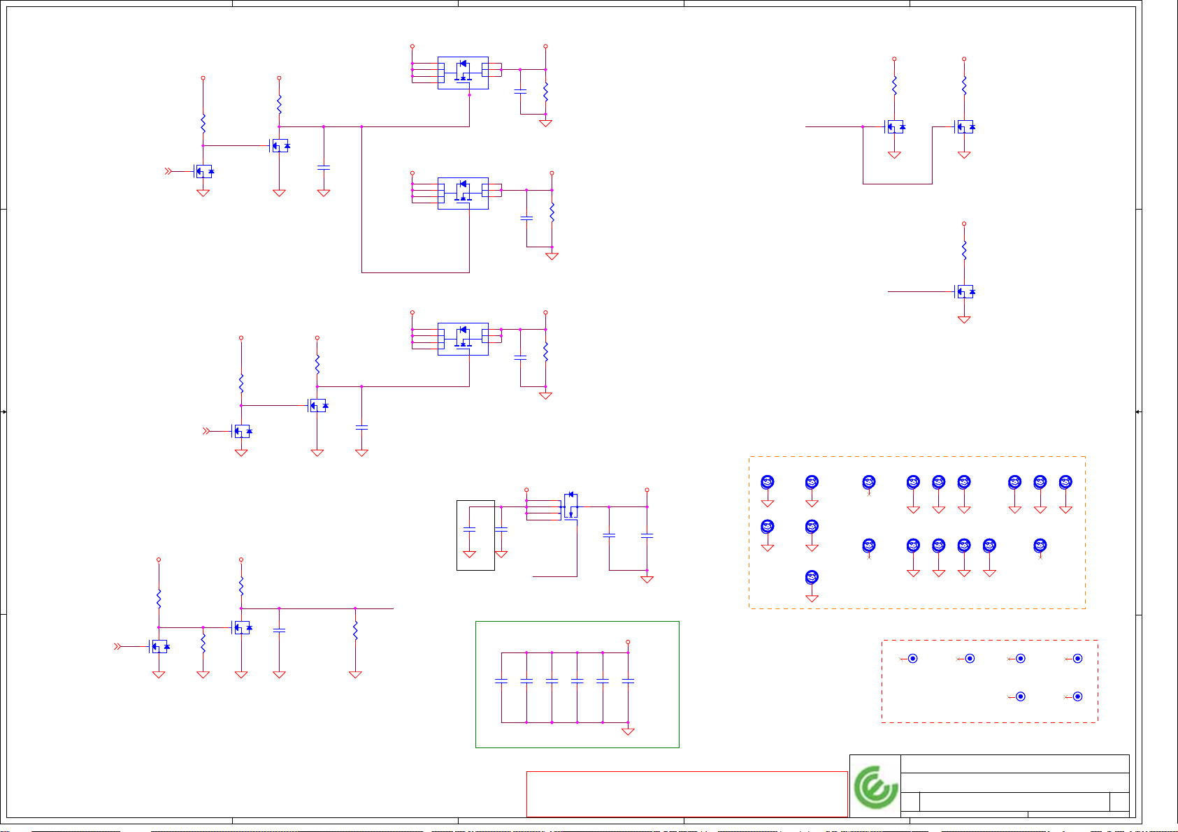
5
+15V_ALW+3.3V_ALW2
12
R171
R171
100K_0402_5%~D
13
D
D
2
G
G
S
S
R197
R197
100K_0402_5%~D
100K_0402_5%~D
SUS_ON_5V#
R283
R283
100K_0402_5%~D
100K_0402_5%~D
2N7002W-7-F_SOT323-3~D
2N7002W-7-F_SOT323-3~D
1
Q27
Q27
2
100K_0402_5%~D
Q14
Q14
2N7002W-7-F_SOT323-3~D
2N7002W-7-F_SOT323-3~D
2
G
G
C248
C248
4700P_0402_25V7K~D
4700P_0402_25V7K~D
2
G
G
Q15
Q15
DK_SUSON<6>
R284
R284
100K_0402_5%~D
100K_0402_5%~D
12
R172
R172
100K_0402_5%~D
100K_0402_5%~D
RUN_ON_5V#
13
D
D
S
S
2
G
G
Q21
Q21
+DOCK_PWR_BAR+DOCK_PWR_BAR
2
200K_0402_5%~D
200K_0402_5%~D
12
G
G
R286
R286
12
13
D
D
S
S
12
13
D
D
S
S
D D
DK_RUNON<6,7>
2N7002W-7-F_SOT323-3~D
2N7002W-7-F_SOT323-3~D
C C
2N7002W-7-F_SOT323-3~D
2N7002W-7-F_SOT323-3~D
B B
12
13
D
D
AUX_ON<6>
2N7002W-7-F_SOT323-3~D
2N7002W-7-F_SOT323-3~D
A A
2
G
G
Q28
Q28
S
S
RUN_ENABLE
1
2
+15V_ALW+3.3V_ALW2
12
R196
R196
100K_0402_5%~D
100K_0402_5%~D
13
D
D
S
S
Q20
Q20
4
C163
C163
4700P_0402_25V7K~D
4700P_0402_25V7K~D
2N7002W-7-F_SOT323-3~D
2N7002W-7-F_SOT323-3~D
ENAB_3VLAN
RUN_ENABLE
1
C166
C166
2
4700P_0402_25V7K~D
4700P_0402_25V7K~D
12
R285
R285
470K_0402_5%~D
470K_0402_5%~D
+5V_ALW +5V_RUN
Q11
Q11
SI4800BDY-T1-E3_SO8~D
SI4800BDY-T1-E3_SO8~D
+3.3V_ALW
SUS_ENABLE
8
D
7
D
6
D
5
D
Q16
Q16
SI4800BDY-T1-E3_SO8~D
SI4800BDY-T1-E3_SO8~D
8
D
7
D
6
D
5
D
Q22
Q22
SI4800BDY-T1-E3_SO8~D
SI4800BDY-T1-E3_SO8~D
8
D
7
D
6
D
5
D
1
S
2
S
3
S
G
4
1
S
2
S
3
S
G
4
1
S
2
S
3
S
G
4
4.7U_0805_10V4Z~D
4.7U_0805_10V4Z~D
2
2
C246
C246
1
1
1
C70
C70
2
0.1U_0402_16V4Z~D
0.1U_0402_16V4Z~D
1
C162
C162
2
10U_0805_10V4Z~D
10U_0805_10V4Z~D
C164
C164
10U_0805_10V4Z~D
10U_0805_10V4Z~D
1
C167
C167
2
10U_0805_10V4Z~D
10U_0805_10V4Z~D
+3.3V_ALW
0.1U_0402_16V4Z~D
0.1U_0402_16V4Z~D
C247
C247
C80
C80
0.1U_0402_16V4Z~D
0.1U_0402_16V4Z~D
1
2
1
2
12
+3.3V_RUN
12
+3.3V_SUS+3.3V_ALW
12
SI3456BDV-T1-E3_TSOP6~D
SI3456BDV-T1-E3_TSOP6~D
6
2
1
ENAB_3VLAN
1
C82
C82
2
0.1U_0402_16V4Z~D
0.1U_0402_16V4Z~D
3
+5V_RUN Source
Design current: 200mA
Max current: 200mA
R170
R170
20K_0402_5%~D
20K_0402_5%~D
R173
R173
+3.3V_RUN Source
Design current: 300mA
20K_0402_5%~D
20K_0402_5%~D
Max current: 300mA
+3.3V_SUS Source
Design current: 200mA
R198
R198
20K_0402_5%~D
20K_0402_5%~D
Max current: 300mA
Q26
Q26
D
D
S
S
45
10U_0805_10V4Z~D
3
1
2
1
2
+DOCK_PWR_BAR
1
C86
C86
2
0.1U_0402_16V4Z~D
0.1U_0402_16V4Z~D
10U_0805_10V4Z~D
C249
C249
1
C87
C87
2
0.1U_0402_16V4Z~D
0.1U_0402_16V4Z~D
G
G
C85
C85
0.1U_0402_16V4Z~D
0.1U_0402_16V4Z~D
+3.3V_LAN
2
RUN_ON_5V#
2
G
G
12
R168
R168
1K_0402_5%~D
1K_0402_5%~D
@
@
13
D
D
Q12
Q12
S
S
@
@
2N7002W-7-F_SOT323-3~D
2N7002W-7-F_SOT323-3~D
SUS_ON_5V#
2
G
G
2
G
G
+3.3V_RUN+5V_RUN
12
R169
R169
1K_0402_5%~D
1K_0402_5%~D
@
@
13
D
D
S
S
+3.3V_SUS
12
R194
R194
1K_0402_5%~D
1K_0402_5%~D
@
@
13
D
D
S
S
Q13
Q13
@
@
2N7002W-7-F_SOT323-3~D
2N7002W-7-F_SOT323-3~D
Q18
Q18
@
@
2N7002W-7-F_SOT323-3~D
2N7002W-7-F_SOT323-3~D
1
SCREW HOLE
H5
CLIP1
CLIP3
CLIP3
CLIP_4P9X2P4
CLIP_4P9X2P4
CLIP5
0.1U_0402_16V4Z~D
0.1U_0402_16V4Z~D
2
C250
C250
1
CLIP5
CLIP_6P2X2P9
CLIP_6P2X2P9
CLIP2
CLIP2
CLIP_4X2P4
CLIP_4X2P4
1
1
1
CLIP4
CLIP4
CLIP_6P2X2P9
CLIP_6P2X2P9
1
CLIP6
CLIP6
CLIP_4P9X2P4
CLIP_4P9X2P4
1
CLIP1
EMI-79x138
EMI-79x138
1
H11
H11
H_1P3X3P3N@
H_1P3X3P3N@
1
H1
H2
H3
H3
3P0@H13P0@
1
H8
3P0@H83P0@
1
3P0@
3P0@H23P0@
3P0@
1
1
H9
H10
H10
3P0@H93P0@
3P0@
3P0@
1
1
H5
3P0@
3P0@
1
H14
H14
3P8@
3P8@
1
H7
H7
H6
3P0@
3P0@
3P0@H63P0@
1
1
H16
H16
5P1N@
5P1N@
1
FIDUCIAL MARK
FD4
FD1
FD1
1
FIDUCAL
FIDUCAL
FD2
FD2
1
FIDUCAL
FIDUCAL
FD3
FD3
1
FIDUCAL
FIDUCAL
FD5
FD5
1
FIDUCAL
FIDUCAL
FD4
1
FIDUCAL
FIDUCAL
FD6
FD6
1
FIDUCAL
FIDUCAL
DELL CONFIDENTIAL/PROPRIETARY
Compal Electronics, Inc.
Compal Electronics, Inc.
Title
Title
PROPRIETARY NOTE: THIS SHEET OF ENGINEERING DRAWING AND SPECIFICATIONS CONTAINS CONFIDENTIAL
TRADE SECRET AND OTHER PROPRIETARY INFORMATION OF DELL INC. ("DELL") THIS DOCUMENT MAY NOT
BE TRANSFERRED OR COPIED WITHOUT THE EXPRESS WRITTEN AUTHORIZATION OF DELL. IN ADDITION,
NEITHER THIS SHEET NOR THE INFORMATION IT CONTAINS WAY BE USED BY OR DISCLOSED TO ANY THIRD
PARTY WITHOUT DELL'S EXPRESS WRITTEN CONSENT.
5
4
3
2
Title
Size Document Number Rev
Size Document Number Rev
Size Document Number Rev
Date: Sheet
Date: Sheet
Date: Sheet
Compal Electronics, Inc.
EE Power
EE Power
EE Power
LA-3954P
LA-3954P
LA-3954P
Friday, April 18, 2008
Friday, April 18, 2008
Friday, April 18, 2008
X03
X03
17
17
17
1
X03
29
29
29
of
of
of
Page 18

5
DOCK_PSID
FBMJ4516HS720NT 1806~D
PJPDC1
PJPDC1
9
GND_4
D D
+DOCK_DC_IN
NB_DET#<5>
PR65
@PR65
@
40.2K_0402_1%~D
40.2K_0402_1%~D
C C
1. Populated PR68
2. Reserve delay circuir, no stuff.
PR59
@ PR59
@
200K_0402_5%~D
200K_0402_5%~D
12
PR60
@ PR60
@
200K_0402_5%~D
200K_0402_5%~D
PR61
@PR61
@
12
0_0402_5%~D
0_0402_5%~D
12
5
12
12
@
@
8
7
6
FOX_JPD113D-DB570-7F
FOX_JPD113D-DB570-7F
PD12
@ PD12
@
RB751V_SOD323~D
RB751V_SOD323~D
PR62
@ PR62
@
200K_0402_5%~D
200K_0402_5%~D
12
3
PC44
PC44
@
@
PQ19B
PQ19B
@
@
4
2N7002DW-T/R7_SOT363-6~D
2N7002DW-T/R7_SOT363-6~D
PC43
PC43
0.047U_0603_16V4Z~D
0.047U_0603_16V4Z~D
GND_3
GND_2
GND_1
21
12
12
DETECT
DC+_1
DC+_2
DC-_1
DC-_2
PR64
@PR64
@
1K_0402_5%~D
1K_0402_5%~D
12
PC45
PC45
@
@
10U_1206_25V6M~D
10U_1206_25V6M~D
5
1
2
3
4
61
2
12
PR63
PR63
@
@
100K_0402_5%~D
100K_0402_5%~D
10U_1206_25V6M~D
10U_1206_25V6M~D
2
FBMJ4516HS720NT 1806~D
FBMJ4516HS720NT 1806~D
FBMJ4516HS720NT 1806~D
FBMJ4516HS720NT 1806~D
FBMJ4516HS720NT 1806~D
1
1
PD1
PD1
@
@
2
2
VZ0603M260APT_0603
VZ0603M260APT_0603
12
PR68
PR68
0_0402_5%~D
0_0402_5%~D
PQ19A
@PQ19A
@
2N7002DW-T/R7_SOT363-6~D
2N7002DW-T/R7_SOT363-6~D
DOCK_AC_OFF<5>
PQ6B
PQ6B
4 3
IMD2AT-108_SC74-6~D
IMD2AT-108_SC74-6~D
4
This Capacitor should be
used only as last resort
for EMI suppression.
Capacitance should be as
small as possible.
PL5
PL5
1 2
PL1
PL1
1 2
PL2
PL2
1 2
PL6
PL6
FBMJ4516HS720NT 1806~D
FBMJ4516HS720NT 1806~D
1 2
PD2
PD2
@
@
VZ0603M260APT_0603
VZ0603M260APT_0603
5
3
Dock DC_IN
+DOCK_DC_IN_SS
1 2
PR6
PR6
12
PR4
PR4
12
1M_0402_5%~D
1M_0402_5%~D
12
13
D
D
2
G
G
S
S
PQ1 P_FDS6681Z_SO8~DPQ1 P_FDS6681Z_SO8~D
1
2
3
4
1M_0402_5%~D
1M_0402_5%~D
PR7
PR7
22K_0402_1%~D
22K_0402_1%~D
2
G
G
12
PC7
PC7
0.1U_0603_50V4Z~D
0.1U_0603_50V4Z~D
PQ10
PQ10
RHU002N06_SOT323
RHU002N06_SOT323
5
12
13
D
D
RHU002N06_SOT323
RHU002N06_SOT323
PQ7
PQ7
S
S
+DOCK_DC_IN_SS
12
PR12
PR12
100K_0402_1%~D
100K_0402_1%~D
12
PR15
PR15
16.5K_0402_1%~D
16.5K_0402_1%~D
3
+DOCK_DC_IN
12
12
PC2
PR2
PR2
@ PC2
@
0.1U_0603_25V7K~D
0.1U_0603_25V7K~D
240K_0402_5%~D
240K_0402_5%~D
2
16
5
PQ3A
PQ3A
IMD2AT-108_SC74-6~D
IMD2AT-108_SC74-6~D
16
PQ6A
PQ6A
IMD2AT-108_SC74-6~D
IMD2AT-108_SC74-6~D
PQ3B
PQ3B
4 3
PC6
PC6
0.022U_0805_50V7K~D
0.022U_0805_50V7K~D
IMD2AT-108_SC74-6~D
IMD2AT-108_SC74-6~D
PR9
PR9
100K_0402_1%~D
100K_0402_1%~D
B540C~D
B540C~D
2 1
PQ2 P_FDS6681Z_SO8~DPQ2 P_FDS6681Z_SO8~D
5
PR8
PR8
12
PR10
PR10
12.1K_0402_1%~D
12.1K_0402_1%~D
PU1
PU1
1 2
LM431SBCMF_SOT23-3
LM431SBCMF_SOT23-3
PD10
PD10
10K_0402_1%~D
10K_0402_1%~D
1 2
12
12
4
PR13
PR13
PR16
PR16
30K_0402_1%~D
30K_0402_1%~D
10K_0402_1%~D
10K_0402_1%~D
+DOCK_SDC_IN
1
2
3
PR5
PR5
1 2
4.99K_0402_1%~D
4.99K_0402_1%~D
PR55
PR55
@
@
0_0402_5%~D
0_0402_5%~D
PR11
PR11
240K_0402_5%~D
240K_0402_5%~D
2
G
G
PQ11
PQ11
NTS4001NT1G_SC70-3
NTS4001NT1G_SC70-3
1 2
1 2
13
D
D
S
S
2
PR1
PR1
0.01_2512_1%~D
0.01_2512_1%~D
1
2
+DOCK_DC_IN
PR54
PR54
12
0_0402_5%~D
0_0402_5%~D
PD3
PD3
RB751V_SOD323~D
RB751V_SOD323~D
PR14
PR14
43K_0402_5%
43K_0402_5%
4
3
21
12
PC8
PC8
12
PR17
PR17
56K_0402_5%~N
56K_0402_5%~N
0.047U_0402_16V5K~D
0.047U_0402_16V5K~D
12
PC3
PC3
PR3
PR3
0.01U_0603_25V7K~D
0.01U_0603_25V7K~D
PQ4
PQ4
NTR4502PT1G_SOT23-3~D
NTR4502PT1G_SOT23-3~D
1
3
1
3
1 3
PR46
PR46
12
100K_0402_5%~D
100K_0402_5%~D
2
2
2
NTR4502PT1G_SOT23-3~D
NTR4502PT1G_SOT23-3~D
PR57
PR57
100K_0402_5%~D
100K_0402_5%~D
2
G
G
13
D
D
RHU002N06_SOT323
RHU002N06_SOT323
2
PQ9
PQ9
G
G
S
S
1 2
1 2
4.7K_0805_5%~D
4.7K_0805_5%~D
PQ5
PQ5
1
1
1 3
2
12
13
12
PC4
PC4
0.1U_0603_50V4Z~D
0.1U_0603_50V4Z~D
3
3
12
2
2
D
D
RHU002N06_SOT323
RHU002N06_SOT323
PQ18
PQ18
S
S
RHU002N06_SOT323
RHU002N06_SOT323
12
PC1
PC1
0.1U_0603_50V4Z~D
0.1U_0603_50V4Z~D
DOCK_DCIN_IS+ <5>
PR56
PR56
100K_0402_5%~D
100K_0402_5%~D
2
G
G
PQ8
PQ8
1
+DOCK_PWR_BAR
12
PC5
PC5
10U_1206_25V6M~D
10U_1206_25V6M~D
DOCK_DCIN_IS- <5>
12
13
D
D
PR69
PR69
0_0402_5%~D
0_0402_5%~D
@
@
S
S
12
PR66
PR66
0_0402_5%~D
0_0402_5%~D
ACAV_DOCK_SRC# <5>
PR67
@ PR67
@
1 2
0_0402_5%~D
0_0402_5%~D
DOCK_DET_1 <5>
Dock PS_ID Detector
B B
PR18
PR18
0_0402_5%~D@
0_0402_5%~D@
1 2
PQ12
DOCK_PSID DOCK_PS_ID
PR21
2
PD5
PD5
SM24_SOT23
SM24_SOT23
@
@
A A
PR21
3
1
1 2
100K_0402_1%~D
100K_0402_1%~D
PR24
PR24
1 2
15K_0402_1%~D
15K_0402_1%~D
5
1 3
2
D
D
B
B
PQ12
S
S
FDV301N_NL_SOT23-3~D
FDV301N_NL_SOT23-3~D
G
G
2
C
C
PQ13
PQ13
PMBT3904_SOT23~D
PMBT3904_SOT23~D
E
E
3 1
PR20
PR20
33_0402_5%~D
33_0402_5%~D
1 2
PD4
PD4
+5V_ALW
DA204U_SOT323~D
DA204U_SOT323~D
+5V_ALW
PR22
PR22
+3.3V_ALW
2
3
1
12
10K_0402_1%~D
10K_0402_1%~D
PR23
PR23
100_0402_5%~D@
100_0402_5%~D@
1 2
4
PR19
PR19
2.2K_0402_5%~D
2.2K_0402_5%~D
PD6
PD6
1 2
+5V_ALW
DA204U_SOT323~D
DA204U_SOT323~D
2
3
1
+DOCK_DC_IN_SS
DOCK_PS_ID <5>
PS_ID_DISABLE# <6>
PD11
PD11
12
RB751V-40_SOD323~D
RB751V-40_SOD323~D
+NBDOCK_DC_IN_SS <5>
4
PU11A
PU11A
LM393DR_SO8~D
LM393DR_SO8~D
2
G
IN-
1
O
3
IN+
P
8
+5V_ALW
PROPRIETARY NOTE: THIS SHEET OF ENGINEERING DRAWING AND SPECIFICATIONS CONTAINS CONFIDENTIAL
TRADE SECRET AND OTHER PROPRIETARY INFORMATION OF DELL INC. ("DELL") THIS DOCUMENT MAY NOT
BE TRANSFERRED OR COPIED WITHOUT THE EXPRESS WRITTEN AUTHORIZATION OF DELL. IN ADDITION,
NEITHER THIS SHEET NOR THE INFORMATION IT CONTAINS WAY BE USED BY OR DISCLOSED TO ANY THIRD
PARTY WITHOUT DELL'S EXPRESS WRITTEN CONSENT.
3
+DOCK_DC_IN 5V_3V_REF
PR143
PR143
1 2
12
PC41
PC41
1 2
100P_0402_50V8J
100P_0402_50V8J
PR146
PR146
232K_0402_1%~D
232K_0402_1%~D
PC42
PC42
21.5K_0402_1%~D
21.5K_0402_1%~D
PR144
PR144
32.4K_0402_1%~D
32.4K_0402_1%~D
1 2
12
1 2
100P_0402_50V8J
100P_0402_50V8J
1M_0402_1%~D
1M_0402_1%~D
1 2
PR147
PR147
100K_0402_1%~D
100K_0402_1%~D
2
5
6
PR145
PR145
0_0402_5%~D
0_0402_5%~D
1 2
+3.3V_ALW
12
PR58
PR58
100K_0402_5%~D
100K_0402_5%~D
ACAV_IN_DOCK <6>
PR142
PR142
+5V_ALW
8
P
IN+
7
O
IN-
G
PU11B
PU11B
LM393DR_SO8~D
LM393DR_SO8~D
4
2V* 100K/ (100K+32.4K)=1.51V
17.8V*21.5K/(232K+21.5K)= 1.51V
DELL CONFIDENTIAL/PROPRIETARY
Title
Title
Title
Size Document Number Rev
Size Document Number Rev
Size Document Number Rev
LA-3954P
LA-3954P
LA-3954P
Date: Sheet
Date: Sheet
Date: Sheet
Compal Electronics, Inc.
Compal Electronics, Inc.
Compal Electronics, Inc.
Power DC-DC
Power DC-DC
Power DC-DC
18 29Friday, April 18, 2008
18 29Friday, April 18, 2008
1
18 29Friday, April 18, 2008
X03
X03
X03
of
of
of
Page 19

5
4
3
2
1
+3.3V_ALWP/ +5V_ALWP/ +5V_ALW2 / +15V_ALWP
Place these CAPs
PJP1
PJP1
+DOCK_PWR_BAR
D D
5 Volt +/-5%
Design current: 4.7A
Max current:6.7A
OCP_min= 7.14A
C C
B B
+5V_ALWP
PC24
PC24
The p-p inductor ripple current/2=1.4A
VILIM1/10= 5uA*110K=55mV
consider 20% tolerance,55mV*80%=44mV 55mV*120%=66mV
OCP(min)=44mV/(5.9mOHM (Rds(on, typ)*1.3)+1.4A=7.14A
OCP(max)=66mV/(5.9mOHM*1.3)+1.4A=10A
1 2
PAD-OPEN 4x4m
PAD-OPEN 4x4m
1
1
PC9
PC10
2
@ PC9
@
@ PC10
@
10U_1206_25V6M~D
10U_1206_25V6M~D
10U_1206_25V6M~D
10U_1206_25V6M~D
12
1
1
+
+
+
+
PC26
PC26
PC25
PC25
2
2
@
@
0.1U_0603_25V7K~D
330U_D3L_6.3VM_R25~D
330U_D3L_6.3VM_R25~D
0.1U_0603_25V7K~D
330U_D3L_6.3VM_R25~D
330U_D3L_6.3VM_R25~D
PR36
0_0603_1%
0_0603_1%
12
12
@ PR36
@
PC36
PC36
12
2200P_0402_50V7K~D
2200P_0402_50V7K~D
PR40
PR40
0_0603_1%~D
0_0603_1%~D
GNDA_3V5V
1
1
PC12
PC12
PC11
PC11
2
2
2
10U_1206_25V6M~D
10U_1206_25V6M~D
10U_1206_25V6M~D
10U_1206_25V6M~D
PC37
@ PC37
@
0.1U_0603_25V7K~D
0.1U_0603_25V7K~D
PR50
@ PR50
@
3.3K_1206_5%~D
3.3K_1206_5%~D
PL4
PL4
3.3UH_SIL1045R-3R3PF_8.2A_30%
3.3UH_SIL1045R-3R3PF_8.2A_30%
1 2
PR52
PR52
4.7_1206_5%~D
4.7_1206_5%~D
PC39
PC39
680p_0603_50VNPO~D
680p_0603_50VNPO~D
close to FETs
12
12
PC14
PC14
PC13
PC13
2200P_0402_50V7K~D
2200P_0402_50V7K~D
0.1U_0805_50V7K~D
0.1U_0805_50V7K~D
12
8
12
12
12
DOCK_POR_RST#<5>
D6D5D7D
G
S
S
S
3
2
1
578
3 6
241
PQ14
PQ14
FDS8880_NL_SO8~D
FDS8880_NL_SO8~D
4
PQ16
PQ16
FDS6676AS_NL_SO8~D
FDS6676AS_NL_SO8~D
PD13
PD13
2 1
RB751V_SOD323~D
RB751V_SOD323~D
DC1_PWR_SRC
POK1
PR45
PR45
1 2
10K_0402_1%~D
10K_0402_1%~D
12
GNDA_3V5V
+5V_ALWP
PC32
PC32
PC46
PC46
PR25
PR25
0_0805_5%~D
0_0805_5%~D
PC19
PC19
0.1U_0603_25V7K~D
0.1U_0603_25V7K~D
GNDA_3V5V
+5V_ALW_UGATE
+5V_ALW_PHASE
PC23
PC23
2
3
BAT54SW-7-F_SOT323~D
BAT54SW-7-F_SOT323~D
12
2
3
0.1U_0603_25V7K~D
0.1U_0603_25V7K~D
BAT54SW-7-F_SOT323~D
BAT54SW-7-F_SOT323~D
0.1U_0603_25V7K~D
0.1U_0603_25V7K~D
PR26
PR26
1 2
0_0805_5%~D
0_0805_5%~D
1 2
GNDA_3V5V
PC22
@PC22
@
0.1U_0402_10V7K~D
0.1U_0402_10V7K~D
PR34
PR34
1 2
110K_0402_1%~D
110K_0402_1%~D
12
PR38
PR38
0.1U_0603_25V7K~D
0.1U_0603_25V7K~D
1_0603_5%~D
1_0603_5%~D
1 2
+5V_ALW_LGATE
1 2
1
PD7
PD7
0.1U_0603_25V7K~D
0.1U_0603_25V7K~D
1
1 2
PD8
PD8
1 2
+3.3V_ALW2
+3.3V_ALW2
PC20
PC20
1U_0402_6.3V6K~D
1U_0402_6.3V6K~D
1 2
Use 0.1uF for ISL6236.
Use 1uF for MAX8778.
PU2
PU2
12
9
BYP
10
OUT1
11
FB1
12
ILIM1
13
PGOOD1
14
ON1
15
DH1
16
LX1
GNDA_3V5V
+5V_ALW_BOOT
PC30
PC30
0.1U_0603_25V7K~D
0.1U_0603_25V7K~D
PC33
PC33
PD9
PD9
2
BAT54CW_SOT323-3~D
BAT54CW_SOT323-3~D
+3P3V_+5V_PWR_SRC
EN_3V_5V
1
4
5
7
8
6
3
IN
REF
RTC
LDO
TON2VCC
ONLDO
LDOREFIN
PGOOD2
MAX8778ETJ+_TQFN32_5X5~D
MAX8778ETJ+_TQFN32_5X5~D
BST117DL118VDD19SECFB20AGND21PGND22DL223BST2
PAD
33
1
24
+3.3V_ALW_BOOT
GNDA_3V5V
+5V_ALW2
3
+5V_ALW2
PC17
PC17
0_0402_5%~D@
0_0402_5%~D@
REFIN2
ILIM2
OUT2
SKIP#
PR27
PR27
10_0603_5%~D
10_0603_5%~D
12
4.7U_0805_10V6K~D
4.7U_0805_10V6K~D
PR30
PR30
1 2
PR31
@PR31
@
0_0402_5%~D
0_0402_5%~D
1 2
PC21
PC21
0.1U_0402_10V7K~D
0.1U_0402_10V7K~D
1 2
5V_3V_REF
51K_0402_1%~D
51K_0402_1%~D
32
31
<BOM Structure>
<BOM Structure>
30
29
28
EN_3V_5VEN_3V_5V
27
ON2
+3.3V_ALW_UGATE
26
DH2
+3.3V_ALW_PHASE
25
LX2
PR39
PR39
1_0603_5%~D
1_0603_5%~D
1 2
2 1
PAD-OPEN 2x2m~D
PAD-OPEN 2x2m~D
GNDA_3V5V
+3.3V_ALWP_REFIN2
No Install for ISL6236
Install 10 ohm for MAX8778
+5V_VCC1
12
PR28
PC27
PC27
PR28
@
@
PR32
PR32
@
@
GNDA_3V5V
POK2
GNDA_3V5V
0.1U_0603_25V7K~D
0.1U_0603_25V7K~D
12
PC18
PC18
1U_0603_10V6K~D
1U_0603_10V6K~D
GNDA_3V5V
PR33
PR33
1 2
PR35
PR35
1 2
0_0402_5%~D
0_0402_5%~D
12
+3.3V_ALW_LGATE
PJP2
PJP2
POK2
0_0402_5%~D
0_0402_5%~D
0_0402_5%~D
0_0402_5%~D
12
12
PR29
PR29
0_0402_5%~D
0_0402_5%~D
12
GNDA_3V5V
12
PC31
@ PC31
@
0.1U_0603_25V7K~D
0.1U_0603_25V7K~D
+3.3V_ALWP
PR43
PR43
100K_0402_5%~D
100K_0402_5%~D
FDS6982AS_NL_SO8~D
FDS6982AS_NL_SO8~D
+3.3V_ALWP
PR44
@ PR44
@
1 2
1 2
100K_0402_5%~D
100K_0402_5%~D
PQ15
PQ15
4
2
Place these CAPs
close to FETs
12
12
PC15
PC15
PC16
PC16
0.1U_0805_50V7K~D
0.1U_0805_50V7K~D
2200P_0402_50V7K~D
2200P_0402_50V7K~D
12
PC38
@ PC38
@
0.1U_0603_25V7K~D
0.1U_0603_25V7K~D
12
PR51
@ PR51
@
3.3K_1206_5%~D
5
D16D1
G1
S1
D2
D2
G2
S2
1
The p-p inductor ripple current/2=0.46A
VILIM1/10= 5uA*51K=25.5mV
consider 20% tolerance,25.5mV*80%=20.4mV 25.5mV*120%=30.6mV
OCP(min)=25.5mV/(16mOHM (Rds(on, typ)*1.3)+0.46A=1.68A
OCP(max)=30.6mV/(16mOHM*1.3)+0.46A=1.93A
3.3K_1206_5%~D
PL3
PL3
3
8.2UH_FDV0630-8R2M=P3 3.7A_20%
8.2UH_FDV0630-8R2M=P3 3.7A_20%
7
8
12
PR53
PR53
4.7_1206_5%
4.7_1206_5%
12
PC40
PC40
680p_0603_50VNPO~D
680p_0603_50VNPO~D
3.3 Volt +/-5%
Design current: 0.4A
Max current: 0.57A
OCP_min= 2.2A
12
12
PR37
PR37
0_0603_1%~D
0_0603_1%~D
12
PR41
@ PR41
@
0_0603_1%~D
0_0603_1%~D
GNDA_3V5V
PC35
PC35
12
2200P_0402_50V7K~D
2200P_0402_50V7K~D
PC28
PC28
0.1U_0603_25V7K~D
0.1U_0603_25V7K~D
+3.3V_ALWP
12
1
+
+
PC29
PC29
2
330U_D3L_6.3VM_R25~D
330U_D3L_6.3VM_R25~D
PR47
PR48
PR48
200K_0402_1%~D
200K_0402_1%~D
+15V_ALWP
PJP3
+15V_ALWP
+5V_ALWP
A A
+3.3V_ALWP
PJP3
PAD-OPEN1x1m
PAD-OPEN1x1m
PJP4
PJP4
1 2
PAD-OPEN 4x4m
PAD-OPEN 4x4m
PJP5
PJP5
1 2
PAD-OPEN 4x4m
PAD-OPEN 4x4m
12
+15V_ALW
(100mA,20mils ,Via NO.=1)
(5A,200mils ,Via NO.=10)
+5V_ALW
(7.5A,300mils ,Via NO.=15)
+3.3V_ALW
PC34
PC34
12
0.1U_0603_25V7K~D
0.1U_0603_25V7K~D
12
GNDA_3V5V
PR49
PR49
39K_0402_1%~D
39K_0402_1%~D
1 2
POK1
PR47
0_0402_5%~D
0_0402_5%~D
1 2
VTT_PWRGD <6>
DELL CONFIDENTIAL/PROPRIETARY
Compal Electronics, Inc.
Compal Electronics, Inc.
Title
Title
PROPRIETARY NOTE: THIS SHEET OF ENGINEERING DRAWING AND SPECIFICATIONS CONTAINS CONFIDENTIAL
TRADE SECRET AND OTHER PROPRIETARY INFORMATION OF DELL INC. ("DELL") THIS DOCUMENT MAY NOT
BE TRANSFERRED OR COPIED WITHOUT THE EXPRESS WRITTEN AUTHORIZATION OF DELL. IN ADDITION,
NEITHER THIS SHEET NOR THE INFORMATION IT CONTAINS WAY BE USED BY OR DISCLOSED TO ANY THIRD
PARTY WITHOUT DELL'S EXPRESS WRITTEN CONSENT.
5
4
3
2
Title
Size Document Number Rev
Size Document Number Rev
Size Document Number Rev
Date: Sheet
Date: Sheet
Date: Sheet
Compal Electronics, Inc.
Power 3V/5V
Power 3V/5V
Power 3V/5V
LA-3954P
LA-3954P
LA-3954P
1
X03
X03
19 29Friday, April 18, 2008
19 29Friday, April 18, 2008
19 29Friday, April 18, 2008
X03
of
of
of
Page 20

5
Version Change List ( P. I. R. List )
4
3
2
1
Request
Item Date Solution Description Rev.Page# Title
5,9,
D D
10,11
15 9/5 DELL15
9,10,11 9/6
16
C C
8 9/6 DELL17
18
19
ME 9/6 1.Change JP2 symbol from TYCO_48226-1211 to TYCO_48226-0611.
GG list
GG list
GG list
GG list 9/6 DELL10 Remove it.
Owner
DELL14
DELL
DELL9/6GG list8
Issue Description
Customer Request:
1.Change Y TO B(6pin) Connector for POWER BOARD.
2.Change E-SATA+USB Connector.
3.Change TREBLE USB Connector.
4.Change RJ45+2USB Connector.
Item 2
No-pop the Link Detect Circuit in Audio Section:
U20, U21, U22, U23, U24, U25, U26, U27
Item 3
USB Cost Reduction:
No-pop ESD diodes
Only use 4 TPS2066 switches
Only use 4 150uF caps
Item 4
Pop 1Mohm resistors on USB crystal circuits
(R68 and R77)
Item 5
No-pop the 47K resistors (R215 and R216) on
USB hub reset lines since this signal is pulled
low by the LPC before 3V_SUS comes up.
Item 8
Please remove DC blocking caps C242 and C243 at
U42.These caps are already present on Roush near
the docking connector. Please verify.
2.Change JESATA symbol from TYCO_1759557-2 to TYCO_1909573-3.
3.Change JUSB1 symbol from TYCO_5787617-4 to Foxconn_UB11123-M4-4F.
4.Change JP3 symbol from TYCO_1840021-1 to SUYIN_020181MHBK4M508ZA.
5.Change page from P09-USB Port x6 + E-SATA to P09-USB Port x3 and PS2x2.
6.Change page from P10-RJ45 and PS2x2 to P10-E-SATA+USB Port x1.
7.Add page P11-RJ45+USB Portx2.
NO-POP the U20, U21, U22, U23, U24, U25, U26, U27,C147,C148,C149,
C150,C151,C152,R143,R144,R145,R146 parts
1.JESATA use TPS2066 x1 and 150uF x1.
2.JUSB1 use TPS2066 x2 and 150uF x2.
3.JP3 use TPS2066 x1 and 150uF x1.
4.No-pop ESD Diodes.
Pop 1Mohm resistors R68 and R77.
NO_Pop the 47k resistors R215 and R216.
4layer X00
4layer X00
4layer X00
4layer X00
4layer X00
4layer X00
EE 9/6 COMPAL Remove it.20 9,10,11
21 EE15 9/11 COMPAL
B B
22 6 GG list 9/12 DELL
Remove FUSE (LF453) Parts.
1.Headphones and Microphone detect wrong.
2.Audio input signal short ground.
Item10
Disconnect PCI_RST# from pin 26 on LPC.
1.Change HP_DET and MIC_DET to pulled up.
2.Change JAUD1.9 from Ground to NC pin.
Modify OK.Net:SIO_RESET# Add pull down R183 resistor.
4layer X00
4layer X00
4layer X00
We will use GPIO27 from the LPC to control
the reset of LPC bus. Name the net SIO_RESET#.
23 9
24 5,10,15
25 11
26 11
27 6
A A
schematic
review
schematic
review
schematic
review
schematic
review
schematic
review
9/12 Compal
9/17 Compal
9/12 Compal
9/12 Compal
9/12 Compal
(PS2)These pull up resistors are already present on
Roush.
OR and NOTGate Power add CAPS to GND
DOCK_LED_10#,DOCK_LED_100#
Change current limit resistors
JP3 connector by pass caps alyeady present
SUYIN_020181MHBK4M508ZA
Update DOCK_ID to X02
NO_Pop the 10K resistors R105,R106,R107,R108.
1.Add caps C203,C204,C211,C212 to GND.
2.Change caps packaged size to 0402.
R103,R104 change to 150 ohm.
NO_pop the 0.01U caps C209,C210.
R43 change to No_pop;R52 change to pop.
4layer X00
4layer X00
4layer X00
4layer X00
4layer X00
DELL CONFIDENTIAL/PROPRIETARY
Compal Electronics, Inc.
Compal Electronics, Inc.
Title
Title
PROPRIETARY NOTE: THIS SHEET OF ENGINEERING DRAWING AND SPECIFICATIONS CONTAINS CONFIDENTIAL
TRADE SECRET AND OTHER PROPRIETARY INFORMATION OF DELL INC. ("DELL") THIS DOCUMENT MAY NOT
BE TRANSFERRED OR COPIED WITHOUT THE EXPRESS WRITTEN AUTHORIZATION OF DELL. IN ADDITION,
NEITHER THIS SHEET NOR THE INFORMATION IT CONTAINS WAY BE USED BY OR DISCLOSED TO ANY THIRD
PARTY WITHOUT DELL'S EXPRESS WRITTEN CONSENT.
5
4
3
2
Title
Size Document Number Rev
Size Document Number Rev
Size Document Number Rev
Date: Sheet
Date: Sheet
Date: Sheet
Compal Electronics, Inc.
EE PIR-1
EE PIR-1
EE PIR-1
LA-3954P
LA-3954P
LA-3954P
X03
X03
20 29Friday, April 18, 2008
20 29Friday, April 18, 2008
20 29Friday, April 18, 2008
1
X03
of
of
of
Page 21

5
Version Change List ( P. I. R. List )
4
3
2
1
Request
Item Date Solution Description Rev.Page# Title
D D
12 9/17
13 9/17 DELL29
14 9/17 DELL30
31
14 9/17 DELL
GG list
GG list
GG list
GG list
Owner
DELL28
COMPAL9/17EE22 Add Page22 EE PIR-3.32
33
C C
34 GG list DELL
33 DELL
13 GG list 9/20
B B
34 DELL
13,14 GG list 9/20
9/19 DELL15 GG list
9/1915
Issue Description
Item 11
Please populate the fuse and the diode and no-pop the
0 ohm resistors at the VGA connector.
Item 12
Please populate the fuse and the diode and no-pop the
0 ohm resistors at the DP connector.
Item 13
Please populate the fuse and the diode and no-pop the
0 ohm resistors at the DP connector.
Item 15
Please no-pop R282 since it is popped on
Roush/Maybach.
Add new EE PIR-3 page.
Layout issue Item34
Add no-pop ESD diode between AGND and GND at the
audio connector for ESD purposes.
Layout issue item 37
AUD_DOCK_HP_OUT - Traces change reference planes
between AGND and GND. They need to maintain the
same reference plane throughout their runs. The traces
also do not reference planes for 100 mils. If not, add and
populate 0.1uF capacitors where the traces cross the
moats. See attached picture hp_crossing the moat.jpg for
moat crossings and bypass locations, circled in red
Item 17
Need to no pop R278 (CA_DET pull down). The system
side has(/is adding) a pull down for this net too.
For now no pop, but in the future - may remove.
Item 18
Need to no pop R277, R280 (HPD pull downs). The
system side has pull downs for these nets.
For now no pop, after testing remove.
No-pop the R243,R109 resistors;POP the D2 diode F4 fuse.
No-pop the R244,R117 resistors;POP the D7 diode F2 fuse.
No-pop the R245,R124 resistors;POP the D9 diode F3 fuse.
No-pop the R282 resistor.
Add D8 ESD diode between AGND and GND at
Audio connector.
Add the C165,C183 0.1uF caps.
No-pop the R278 resistor (CA_DET pull down).
No-pop the R277,R280 resistors (HPD pull downs).
4layer X00
4layer X00
4layer X00
4layer X00
4layer X00
4layer X00
4layer X00
4layer X00
4layer X00
8 GG list35 9/20 No-pop the R72,R73 resistors.
DELL
Item 19
We need to no-pop one pair of the pull-up resistors for the
keep one pair of the pull-up resistor for the USB SMBus.
4layer X00
USB SMBus. There are two pairs of pull-ups on this bus.
6,836 EE 11/5
Benson
Test Crystal EA fail.modify the circuit.
Recommend circuit:
1.Change Y1 part from 24MHZ_20PF_1BX24000BK1A~D to 24MHZ_12PF_1BX24000CE1B~D.
2.Change C27 part from 18P_0402_50V8J~D to 15P_0402_50V8J~D.
3.Change C28 part from 18P_0402_50V8J~D to 12P_0402_50V8J~D.
4layer X01
4.Change C51,C63 part from 12P_0402_50V8J~D to 15P_0402_50V8J~D.
5.Change C50,C62 part from 12P_0402_50V8J~D to 18P_0402_50V8J~D.
37 13 EE 11/06 Benson
A A
DVI port A and port b on DVI board location wrong.
Modify JP4 board to board connector port A,B location.
4layer X01
DELL CONFIDENTIAL/PROPRIETARY
Compal Electronics, Inc.
Compal Electronics, Inc.
Title
Title
PROPRIETARY NOTE: THIS SHEET OF ENGINEERING DRAWING AND SPECIFICATIONS CONTAINS CONFIDENTIAL
TRADE SECRET AND OTHER PROPRIETARY INFORMATION OF DELL INC. ("DELL") THIS DOCUMENT MAY NOT
BE TRANSFERRED OR COPIED WITHOUT THE EXPRESS WRITTEN AUTHORIZATION OF DELL. IN ADDITION,
NEITHER THIS SHEET NOR THE INFORMATION IT CONTAINS WAY BE USED BY OR DISCLOSED TO ANY THIRD
PARTY WITHOUT DELL'S EXPRESS WRITTEN CONSENT.
5
4
3
2
Title
Size Document Number Rev
Size Document Number Rev
Size Document Number Rev
Date: Sheet
Date: Sheet
Date: Sheet
Compal Electronics, Inc.
EE PIR-2
EE PIR-2
EE PIR-2
LA-3954P
LA-3954P
LA-3954P
X03
X03
21 29Friday, April 18, 2008
21 29Friday, April 18, 2008
21 29Friday, April 18, 2008
1
X03
of
of
of
Page 22
5
Version Change List ( P. I. R. List )
4
3
2
1
Request
Item Date Solution Description Rev.Page# Title
10 EE 11/07
D D
Owner
Benson38
39 5 DELL 11/07 Benson
40 15 COMPAL 11/08 Benson
41 6 COMPAL 11/08 Benson
42 6 11/09 Benson
43 6 11/12 Benson
44 6 11/12 Benson
C C
GG list
SCH164847
SCH164844
45 5 11/13SCH164880 Benson
46 6 COMPAL 11/13 Benson
47 6 SCH164886 11/13 Benson
48 5 COMPAL 11/13 Benson
49 17 COMPAL 11/13 Benson
50 15 COMPAL 11/14 Benson
B B
Issue Description
Test SATA EA fail.modify the circuit.
Modify E-DOCK PIN OUT
Audio SM2602 DVSS,AVSS,HPVSS noise.
Change DOCK ID to X03.
U39, U40 use a different schematic symbol for an OR gate
then the U59 from Roush schematics. Compal needs to
standardize on one symbol for an OR gate.
What is being done to prevent the symbol issues seen
on Roush? This needs to be resolved before PT gerber.
No-pop Duplicate Pull-up Resistors on APR
Fix DVI Pinout Issue on APR and DVI Daughter Card.
Passing 3V_ALW to Power Board
Change connector part.
Add Comparator Circuit for AC_AVIN_DOCK.
Follow the POWER PIR2 item 2.
Add EMI CLIP.
Audio EMI test fail.
Net: SATA_SBTX_C_DRX_P_1 and SATA_SBTX_C_DRX_N_1 point add series
connection R308 470ohm.
Add JP1 pin41 pin net: +DOCK_DC_IN_SS.source by P18-PWR_Dock DC_IN/PS_ID.
Change L28,L29,L30 part to 0 ohmresistors .
No-pop the R51 resistor;Pop the R42 resistor.
Change U39,U40 symbol to SN74AHC1G32DCKR_SC70-5~D best on Roush.
Please no-pop the following resistors since they are pulled up on
4layer X01
4layer X01
4layer X01
4layer X01
4layer X01
4layer X01
the system side when docked:R7,R8,R9,R231.
There is a pin define error on the connector pinouts of both APR and DVI
4layer X01
daughtercard that is preventing DVI display.The pinout on JP4 (APR) and
JP1 (DVI board) need to change for proper DVI display on both channels.
DVI Port A should be above Display Port A
DVI Port B should be above Display Port B.
we add Q6 at DOCKED_LED# net and Q7 at BREATH_PWR_LED# net.
Change JP2 symbol from MOLEX_48226-0611 to MOLEX_48227-0611.
Please add a comparator circuit, as outlined in separate email.The output of this comparator circuit
4layer X01
4layer X01
4layer X01
will be named ACAV_IN_DOCK and needs to be routed to a Dock EC GPIO.Use GPIO11 on the APR.
and Remove the R186 part.
Change net "ACAV_IN_DOCK#" to "ACAV_DOCK_SRC#"
ADD CLIP2~CLIP6 Part.
4layer X01
4layer X01
1.Please reserve R71,R79 0 ohm at Dock connector side and AC termination at the End for
I2S_BCLK and I2S_12MHz.
4layer X01
2. I2S_BCLK parallel R234 22 ohm and C195 10P to GND.
2. I2S_12MHZ parallel R235 22 ohm and C199 10P to GND.
51 16 COMPAL 11/15 Bill
MIC bias resistor needs to change from 4.99 ohm to
Change R139 from 4.99ohm to 40.2Kohm.
4layer X01
40Kohm at R139.
52 13,14 COMPAL 11/15 Bill
53 6,8,16 COMPAL 11/19 Benson
Change F2, F3 to 3A_6VDC_2920SMD300 Change F2, F3 to 3A_6VDC_2920SMD300
Have found that high Resistance values at the gate of the
Change the R65,R66,R214 from 10K to 0ohm
SMBus isolation FETs may affect the Vgs turn-on volatge,
4layer X01
4layer X01
causing the SMBus to disconnect unexpectedly because
the isolation FETs are not turning on.
54 13, 14 COMPAL 12/13 Jake Lee
A A
Customer Request:
1.Change resistor for SN75DP122_QFN56~D.
2.Change resistor for SN75DP122_QFN56~D.
1. Change part R202 from 5.11Kto 3.48K.
2. Change part R208 from 5.11Kto 3.48K.
4layer X02
DELL CONFIDENTIAL/PROPRIETARY
Compal Electronics, Inc.
Compal Electronics, Inc.
Title
Title
PROPRIETARY NOTE: THIS SHEET OF ENGINEERING DRAWING AND SPECIFICATIONS CONTAINS CONFIDENTIAL
TRADE SECRET AND OTHER PROPRIETARY INFORMATION OF DELL INC. ("DELL") THIS DOCUMENT MAY NOT
BE TRANSFERRED OR COPIED WITHOUT THE EXPRESS WRITTEN AUTHORIZATION OF DELL. IN ADDITION,
NEITHER THIS SHEET NOR THE INFORMATION IT CONTAINS WAY BE USED BY OR DISCLOSED TO ANY THIRD
PARTY WITHOUT DELL'S EXPRESS WRITTEN CONSENT.
5
4
3
2
Title
Size Document Number Rev
Size Document Number Rev
Size Document Number Rev
Date: Sheet
Date: Sheet
Date: Sheet
Compal Electronics, Inc.
EE PIR-3
EE PIR-3
EE PIR-3
LA-3954P
LA-3954P
LA-3954P
X03
X03
22 29Friday, April 18, 2008
22 29Friday, April 18, 2008
22 29Friday, April 18, 2008
1
X03
of
of
of
Page 23

5
Version Change List ( P. I. R. List )
4
3
2
1
Request
Item Date Solution Description Rev.Page# Title
13, 14, 15COMPAL 12/13
D D
Owner
Jake Lee55
5 COMPAL 12/1956 Jake Lee
16 COMPAL 12/2757 Jake Lee
58 5 COMPAL 12/27 Jake Lee
59 6 COMPAL 01/07 Benson
60 13,14 DELL 01/15 Benson
C C
61 5 DELL 01/14 Benson
62 11 DELL 01/15 Benson
63 9,10,11 DELL 01/15 Benson
64 7 COMPAL 01/16 Benson
65 12 COMPAL 01/29 Benson
B B
Issue Description
Customer Request:
1.Change FUSE part
2.Change SSM2603CPZ
Customer Request:
1. Change resistor for TYCO_1840015-1.
Headphone channels of right and left are exchanging.
The DOCK_POR_RST# signal will now be used to control
the power to the dock.
Change DOCK ID to X02.
Base on Roush Discrete Graphics changes for DP.
The Docking pinout will change to move the DOCK_DET#
and SLICE_BAT_PRES# pins to minimize the false
detection of an attached dock or slice battery when the
system is inserted at an angle
Customer Request
Change COMPAL part.
Parallel capactior change to 0402 capacitor...
Change the ports for CRT EA report.
Customer Request:
1.Change FUSE part
1. Change part F2 from 3A_6VDC to 1.1A_6V.
2. Change part F3 from 3A_6VDC to 1.1A_6V.
3. Change part U17 from SSM2603 to SSM2603.
1. Change part JP3 from SUYIN_020181MHBK4M508ZA to TYCO_1840015-1.
Exchange nets of between the AUD_COCK_HP_OUT_R and the AUD_DOCK_HP_OUT_L.
Add new net of DOCK_POR_RST# to JP1.140.
No-pop the R42 resistor;Pop the R51 resistor.
1. Add 10KOhm POP the PU (R309) and NO-POP the PD (R311) on DPA_DOCK_AUX#.
2. Add 10KOhm NO-POP the PU (R310) and POP the PD (R312) on DPA_DOCK_AUX.
3. Add 10KOhm POP the PU (R313) and NO-POP the PD (R315) on DPB_DOCK_AUX#.
4. Add 10KOhm NO-POP the PU (R314) and POP the PD (R316) on DPB_DOCK_AUX.
Swap pin141 and pin143 on connector.
Swap pin142 and pin144 on connector.
Change L31 to 0 ohm resistor for LOM CT signaling
Change U7,U33,U37,U45 from TPS2066DR_SO8~D to TPS2066ADR_SO8~D0 part.
Change CP1,CP2,CP3,CP4 from Parallel capactior to (C259-C274) 0402
capactior.
Add 2.2pF capacitor to C97~C102 and change L14~L16 to 22 ohm bead
(BK1608HS220T_0603~D).
1. Change part F4 from 3A_6VDC to 1.1A_6V.
4layer X02
4layer X02
4layer X02
4layer X02
4layer X02
4layer X02
4layer X02
4layer X02
4layer X02
4layer X02
4layer X02
4layer X0212 COMPAL 01/2466 Benson
67
15
DELL 2/12 Benson
For customer request.
Power supply filtering for U17 the SSM2603.
1.Change part L21,L25from BK1608LM182-T_0603~D to BLM18EG601SN1D_2P~D.
2.Pin3 and pin5 of U19 are combined together,and remove part C133,C187
and add L25 to keep the power supply clean.
4layer X02
3.Pin12 and pin18 of U19 are combined together,and remove part C124,C125.
Change C126,C129,C131 from 1uF to 10U_0805_10V4Z~D.
68
13,14
DELL 2/14 Benson
For customer request.
Based on a review of the DP spec.we are
considering making changes to the DP
connector power delivery, like adding a
PTC fuse and bulk capacitance on the
1.Change part F2 and F3 from 1.1A_6V_1812L110PR~D to 3A_6VDC_2920SMD300.
2. Add part C128 10U_0805_10V4Z~D at +DPA_VCC net
3. Add part C133 10U_0805_10V4Z~D at +DPB_VCC net
4layer X02
system and dock side.
13,14
A A
DELL 2/14 Benson69
DP BOM Changes to Support PT SMT
R202 and R208 should change to 3.83K for passing DP eye.
4layer X02
DELL CONFIDENTIAL/PROPRIETARY
Compal Electronics, Inc.
Compal Electronics, Inc.
Title
Title
PROPRIETARY NOTE: THIS SHEET OF ENGINEERING DRAWING AND SPECIFICATIONS CONTAINS CONFIDENTIAL
TRADE SECRET AND OTHER PROPRIETARY INFORMATION OF DELL INC. ("DELL") THIS DOCUMENT MAY NOT
BE TRANSFERRED OR COPIED WITHOUT THE EXPRESS WRITTEN AUTHORIZATION OF DELL. IN ADDITION,
NEITHER THIS SHEET NOR THE INFORMATION IT CONTAINS WAY BE USED BY OR DISCLOSED TO ANY THIRD
PARTY WITHOUT DELL'S EXPRESS WRITTEN CONSENT.
5
4
3
2
Title
Size Document Number Rev
Size Document Number Rev
Size Document Number Rev
Date: Sheet
Date: Sheet
Date: Sheet
Compal Electronics, Inc.
EE PIR-4
EE PIR-4
EE PIR-4
LA-3954P
LA-3954P
LA-3954P
X03
X03
23 29Friday, April 18, 2008
23 29Friday, April 18, 2008
23 29Friday, April 18, 2008
1
X03
of
of
of
Page 24

5
Version Change List ( P. I. R. List )
4
3
2
1
Request
Item Date Solution Description Rev.Page# Title
D D
13,14,16 02/19DELL
13, 14 02/19DELL71
Owner
Benson70
Benson
Benson02/1915,16 DELL72
73 12 DELL 4layer X02
ADI 4layer X021.Delete the R23~R26 Part 0_0603_5%~D.
C C
02/19 Benson
02/1974 15,16 Benson
Issue Description
Customer Request:
1.Change Display connector part
2.Change Audio connector part
DP BOM Changes to Support PT SMT
For customer request.
Audio Output protection.
For customer request.
Change CRT FUSE to No_pop.
Recommended by ADI
Enhance ESD test result.
1. Change part JDP1,JDP2 from MOLEX_47272-0001~D to MOLEX_47272-0026.
2. Change part JAUD1 from TYCO_1775390-6 to TYCO_6-1775390-6.
R202 and R208 should change to 3.83K for passing DP eye.
1. Add D35 part.anode to the output Pin13(LHOUT) and the cathode to
pin 12 HPVDD.
2. Add D36 part.anode to the output Pin14(RHOUT) and the cathode to
pin 12 HPVDD.
3. Add one capacitor of around 300pF in parallel with R223 and do the
same for R224, and place these 2 capacitors be close to the U17.
F4 change to No_pop;R109 change to pop.
2.Delete the C165,C183 Part 0.1U_0402_16V7K~D.
3.Delete the L28~L30 Part 0_0603_5%~D.
4.Add the C134 Part 0.1U_0402_16V7K~D at +3.3V_RUN.
5.Add the C132 Part 0.1U_0402_16V7K~D at +3.3V_AVDD.
6.Add the R92 Part 0_0402_5%~D at AGND and DGND.
7.Change the C275 net from HP_SPK_L1 to AUD_DOCK_HP_OUT_L.
8.Change the C276 net from HP_SPK_R1 to AUD_DOCK_HP_OUT_R.
9.Change the C145 net from MIC3 to MIC2.
10.Delete the D26,D27 Part PRTR5V0U2X_SOT143-4~D.
11.Delete the L24 Part BLM18AG121SN1D_0603~D.
12.Delete the R225~R226 Part 0_0402_5%~D.
1.Add C165 0.1uF on SIO_RESET#(near chip side).
2.Add C183 and C183 0.1uF on DP_A_HP and DP_B_HP(near chip side)
4layer X02
4layer X02
4layer X02
4layer X0275 03/046,13,14 COMPAL Benson
03/1076
B B
BensonADI15,16 1.Delete the C134 Part 0.1U_0402_16V7K~D.
Recommended by ADI
2.Change the C126,C131 Part from 10U_0805_10V4Z~D to 4.7U_0805_10V4Z~D.
3.Change C129 Part from 10U_0805_10V4Z~D to 0.1U_0402_16V7K~D.
4layer X02
4.Delete the C275,C276,L23,L22,C137,C138,R141 part.
5.Change the R139 from 40.2K_0402_1%~D to 200_0402_1%~D.
6.Change the C145,1 net from Mic_2 to DOCK_MICIN.by the way change to
1000PF.
03/1077 13 COMPAL Benson
1678
COMPAL 03/12 Benson
Change the ports for DPa EA report.
We review audio schematic found Symbol pin
define mirror.
79 13,14 DELL 03/12 Benson
80 15 COMPAL 03/12 Benson
81 17 COMPAL 03/12 Benson
A A
82 9 COMPAL 03/12 Benson
Change the ports for DPa an DPb EA report.
Recommended by ADI
Modify H14 SCREW HOLE
L4 swap for layout routing issue.
1.Change R202 Part from 3.83K_0402_1%~D to 4.02K_0402_1%~D.
1.Modify JAUD1 symbol.
1.Change R202 Part from 4.02K_0402_1%~D to 3.48K_0402_1%~D.
1.Change R208 Part from 3.83K_0402_1%~D to 3.48K_0402_1%~D.
1.Delete R92 Resister AGND Connect DGND
2.Change L25 part from 0_0805 to BLM18EG601SN1D_2P~D
1.Change H14 from 3P25 to 3P8.
1.L4 swap PIN define.
4layer X02
4layer X02
4layer X02
4layer X02
4layer X02
4layer X02
DELL CONFIDENTIAL/PROPRIETARY
Compal Electronics, Inc.
Compal Electronics, Inc.
Title
Title
PROPRIETARY NOTE: THIS SHEET OF ENGINEERING DRAWING AND SPECIFICATIONS CONTAINS CONFIDENTIAL
TRADE SECRET AND OTHER PROPRIETARY INFORMATION OF DELL INC. ("DELL") THIS DOCUMENT MAY NOT
BE TRANSFERRED OR COPIED WITHOUT THE EXPRESS WRITTEN AUTHORIZATION OF DELL. IN ADDITION,
NEITHER THIS SHEET NOR THE INFORMATION IT CONTAINS WAY BE USED BY OR DISCLOSED TO ANY THIRD
PARTY WITHOUT DELL'S EXPRESS WRITTEN CONSENT.
5
4
3
2
Title
Size Document Number Rev
Size Document Number Rev
Size Document Number Rev
Date: Sheet
Date: Sheet
Date: Sheet
Compal Electronics, Inc.
EE PIR-5
EE PIR-5
EE PIR-5
LA-3954P
LA-3954P
LA-3954P
X03
X03
24 29Friday, April 18, 2008
24 29Friday, April 18, 2008
24 29Friday, April 18, 2008
1
X03
of
of
of
Page 25

5
Version Change List ( P. I. R. List )
4
3
2
1
Request
Item Date Solution Description Rev.Page# Title
D D
17 03/13DELL
Owner
Benson83
84 Benson17 DELL 03/13
85 Benson17 DELL 03/14
86 Benson12 DELL 03/14 4layer X02
15,16 ADI 03/15 4layer X02
87 Benson 1.Change L21 to BLM21PG331SN1D.
C C
Benson15,1687 03/15ADI
88 13,14 04/08 Benson
DELL
Issue Description
EMI Request
APR and add several 0.1µF capacitance from Vcc to GND
and PCI_CLK AC terminal.
Audio jack pin define correct
Change COMPAL part
Change the ports for CRT EA report.
1.Improve Dynamic Range on HP and Mic.
2.Need to adjust Mic Bias to accommodate Bias current of
<750uA
3.System noise is effecting the Microphone performance.
4.Need to meet GS Mark Spec
5.Improve THD on HP
R225,R226 part correct
Add DP to DP repeater.
1. +DOCK_PWR_BAR net New add: 6*0.1µF C80,C82,C85,C86,C87,C70 at BOT
4layer X02
and TOP side.
2. PCI_CLK: change BOM: R60 change to 33 ohm, C29 change to 10P
1.Swap pin1 and pin4 on JAUD1
2.Swap pin2 and pin3 on JAUD1
4layer X02
3.Swap pin6 and pin8 on JAUD1
4.Swap pin5 and pin9 on JAUD1
1.Change C246 part form 4.7U_0603_6.3V4Z~D to 4.7U_0805_10V4Z~D.
4layer X02
Modify 2.2pF capacitor to C97~C102.
2.Change C136 to 2K_0402_5%~D.
3.Connect a cap C88 (10uf) from R136 pin 1 to Analog Ground and connect
a resistor R140 (200ohm) from R136 pin 1 to MICBIAS.
4.Change C135 & C140 to 100uf and the output resistor R225,R226 values
will be 68 Ohms.
5.Connect 2 capacitors C186,C187 of 300pF from pin 13 and pin 14 respectively to
the analog ground on U17. Please make these Nopop for now.
1.Change the R225,R226 to 68_0402_5%~D.
Add U46,U47 8121E parts.
4layer X02
4layer X03
89 13 DELL 04/08 Benson
B B
90 13,14 TI 04/11 Cindy
Remove the about audio no-pop part.
for TI comments.
Remove the U19,U20,U21,U22,U23,U24,U25,U26 part.
1.Change pin8 and 9 of PS8121E from AUX_A_CH+/- to DPA_DOCK_AUX/#.
2.Change HPD flow to DP connector to PS8121 to DP122 to Dock connector (1)Pin18 JDP1
4layer X03
4layer X03
connector feed pin30 PS8121 (HPD_SINK) (2)Pin 7 of PS8121 (HPD) feed pin40 DP122
(DP_HPD_SINK) (3)Pin37 DP122 (HPD) feed pin39 docking station connector
3.Add R139 and R321 to pull high DDCBUF_EN# of PS8121E.
4.remove CA_DET application circuit.
13,1491 Benson04/16DELL
for Dell comments.
1. C182,C183 should be "no-pop" and the value should change to 0.033uF
(0402 pkg).
2. Place pads for a 600 ohm FB (0402 pkg) between JDP1 pin 18 and the
4layer X03
DPA_DOCK_HPD net. Please use a 0 ohm resistor in this location.
3. Place pads for a 600 ohm FB (0402 pkg) between JDP2 pin 18 and the
DPB_DOCK_HPD net. Please use a 0 ohm resistor in this location.
4. Populate the R244,R245 and "no-pop" the D7,D9.
5. Change the R276,R279 to "no-pop".
A A
92 06 COMPAL 04/16 Benson
93 13 DELL 04/18 Benson
5
Change Dock ID form X02 to X03.
for Dell comments.
4
PROPRIETARY NOTE: THIS SHEET OF ENGINEERING DRAWING AND SPECIFICATIONS CONTAINS CONFIDENTIAL
TRADE SECRET AND OTHER PROPRIETARY INFORMATION OF DELL INC. ("DELL") THIS DOCUMENT MAY NOT
BE TRANSFERRED OR COPIED WITHOUT THE EXPRESS WRITTEN AUTHORIZATION OF DELL. IN ADDITION,
NEITHER THIS SHEET NOR THE INFORMATION IT CONTAINS WAY BE USED BY OR DISCLOSED TO ANY THIRD
PARTY WITHOUT DELL'S EXPRESS WRITTEN CONSENT.
1.Change the R44 to "pop" ,R53 to "no-pop".
1.Change the PS_PC0 "R318" and PS_PC1 "R320" to "no-pop".
3
2
DELL CONFIDENTIAL/PROPRIETARY
Compal Electronics, Inc.
Compal Electronics, Inc.
Title
Title
Title
Size Document Number Rev
Size Document Number Rev
Size Document Number Rev
Date: Sheet
Date: Sheet
Date: Sheet
Compal Electronics, Inc.
EE PIR-5
EE PIR-5
EE PIR-5
LA-3954P
LA-3954P
LA-3954P
1
4layer X03
4layer X03
25 29Friday, April 18, 2008
25 29Friday, April 18, 2008
25 29Friday, April 18, 2008
of
of
of
X03
X03
X03
Page 26
5
Version Change List ( P. I. R. List )
4
3
2
1
Request
Item Date Solution Description Rev.Page# Title
94
D D
C C
13,14 04/18Parade
Owner
Benson
Issue Description
for Parade comments.
Please add the ac-coupled capacitor on AUX channel
to PS8121ED
1.Add the C290,C291 AC_coupled capacitor on AUX channel U46 and
add the R322,R323 pull up 100K to 3.3V .
2.Add the C292,C293 AC_coupled capacitor on AUX channel U47 and
add the R324,R325 pull up 100K to 3.3V .
4layer X03
B B
A A
DELL CONFIDENTIAL/PROPRIETARY
Compal Electronics, Inc.
Compal Electronics, Inc.
Title
Title
PROPRIETARY NOTE: THIS SHEET OF ENGINEERING DRAWING AND SPECIFICATIONS CONTAINS CONFIDENTIAL
TRADE SECRET AND OTHER PROPRIETARY INFORMATION OF DELL INC. ("DELL") THIS DOCUMENT MAY NOT
BE TRANSFERRED OR COPIED WITHOUT THE EXPRESS WRITTEN AUTHORIZATION OF DELL. IN ADDITION,
NEITHER THIS SHEET NOR THE INFORMATION IT CONTAINS WAY BE USED BY OR DISCLOSED TO ANY THIRD
PARTY WITHOUT DELL'S EXPRESS WRITTEN CONSENT.
5
4
3
2
Title
Size Document Number Rev
Size Document Number Rev
Size Document Number Rev
Date: Sheet
Date: Sheet
Date: Sheet
Compal Electronics, Inc.
EE PIR-6
EE PIR-6
EE PIR-6
LA-3954P
LA-3954P
LA-3954P
X03
X03
26 29Friday, April 18, 2008
26 29Friday, April 18, 2008
26 29Friday, April 18, 2008
1
X03
of
of
of
Page 27

5
4
Version Change List ( P. I. R. List )
3
2
1
Request
Item Date Solution Description Rev.Page#
117
D D
218
Title
GG list
Derating
issue
Owner
8/2
8/7 Compal
DELL Follow GG_issue_list
+3.3V_ALWP
3
18
Choke Size
8/7
Compal
4 18 EMI 8/9 Compal
5 17 PSL issue 8/15 Compal
C C
6 17 8/15 CompalDC_IN
7 17 DC_IN 8/20 Compal
8 18 Component 9/6 Compal
917
10
17
DC_IN 9/10 Compal
Component
shortage issue
9/12
Compal
Issue Description
Change PR10 and PR12 from 240K to 100K
Change PR11 from 100K to 240K
Change PR13 and PR16 from 240K to 150K
Change PR14 from 100K to 43K
Change PR15 from 240K to 7.87K
Change PR17 from 100K to 56K
Change PC8 from 0.1U to 1U
Add PR140 and PR141.
Because the Vgs rating for RUH002N06 is 20V
and the NB_Det# is 19V.so we need adding
resister to divide the voltage.
Because the power budget is 0.57A_MAX
for *3.3V_ALWP, we change the size for PL3
change location PR52 and PC39 each other
change location PR53 and PC40 each other
The APL431LBAC-TRL for PU1 is not approve
vender base on DELL PSL list
Add PD10 between PQ2.1 and PQ22.8 Add PD10 between PQ2.1 and PQ22.8
Dock supports the 230W adapter. The FDS6679
is not enough to meet current rating. We plan to
change MOS for PQ1 and PQ2.
The FDS6676AS is common part Change PQ16 from FDS6676S to FDS6676AS.
Time seqence setting when NB insert to Docking
The Vender (TI) will material shortage issue for
TL431BQDBZR on PU1
We plan to implement TL431BQDBZR on PT 2nd source
Connect PR140_2 to NB_Det#,
Connect PR140_1 to PR141_2and PQ17_2.
Connect PR141_1 to GND
Change PL3 from 10mm*10mm*4mm to 7mm*7mm*3mm
change location PR52 and PC39 each other
change location PR53 and PC40 each other
Change PU1 from APL431LBAC-TRL(AMPEC) to TL431BQDBZR(TI).
Change PR15 from 7.87K to 16.5K
Change PQ1 and PQ2 from FDS6679 AZ to FDS6681Z
Add PR54 and PR55, no-pop PR54
Change PU1 form TL431BQDBZR (TI)to LM431SBCMF(FIRCHILD)
X01
X01
X01
X01
X01
X01
X01
X02
X02
X02
ACAV_IN
B B
circuit
10/26
DELL
Support E-Dock hot plug/unplug of AC Adapter
1. Change component
PC6 from 0.47U to 0.1U
X0211 17
PR4 from 240K to 1M
PR6 from 47K to 220K
PR7 from 47K to 22K
PR8 from 100K to 10K
PR5 from 100K to 4.99K
PR10 from 100K to 24.9K
PR13 and PR16 from 150K to 30K
PC8 from 1U to .047U
2, Change net name for PR12.1 from +DOCK_SDC_IN to +DOCK_DC_IN_SS
3. Stuff PR54 and un-stuff PR55
12 17 PSID circuit 10/31 Compal Dock PSID signal fail
Change net name from +5VALW to +5V_ALW for PD3_Pin3, PR22_Pin2
X02
and PD5_Pin3
A A
DELL CONFIDENTIAL/PROPRIETARY
Compal Electronics, Inc.
Compal Electronics, Inc.
Title
Title
PROPRIETARY NOTE: THIS SHEET OF ENGINEERING DRAWING AND SPECIFICATIONS CONTAINS CONFIDENTIAL
TRADE SECRET AND OTHER PROPRIETARY INFORMATION OF DELL INC. ("DELL") THIS DOCUMENT MAY NOT
BE TRANSFERRED OR COPIED WITHOUT THE EXPRESS WRITTEN AUTHORIZATION OF DELL. IN ADDITION,
NEITHER THIS SHEET NOR THE INFORMATION IT CONTAINS WAY BE USED BY OR DISCLOSED TO ANY THIRD
PARTY WITHOUT DELL'S EXPRESS WRITTEN CONSENT.
5
4
3
2
Title
Size Document Number Rev
Size Document Number Rev
Size Document Number Rev
Date: Sheet
Date: Sheet
Date: Sheet
Compal Electronics, Inc.
Power PIR
Power PIR
Power PIR
LA-3954P
LA-3954P
LA-3954P
X03
X03
27 29Friday, April 18, 2008
27 29Friday, April 18, 2008
27 29Friday, April 18, 2008
1
X03
of
of
of
Page 28
5
4
Version Change List ( P. I. R. List )
3
2
1
Request
Item Date Solution Description Rev.Page# Title
D D
2
17
ACAV_IN
circuit
ACAV_IN
circuit
17 Comparator
C C
Circuit
4 17 ACAV_IN
11/121 17 DELL X02When no AC adapter is in E-Dock and
11/12
11/123
11/15 DELL EE work item Add PD11 (RB751) X02
Owner
DELL
DELL Add Comparator Circuit X02
circuit
517
ACAV_IN
circuit
11/15 DELL
Issue Description
EN_DOCK_PWR_BAR is low to hold of Roush PQ23,
there is back drive issue where the
+DOCK_PWR_BAR is held up. The issue is that NB
DOCK_DCIN_IS+ and - on the NB side is biased up
to +PWR_SRC potential, this holds the source
terminals of both PQ4, and PQ5 higher than
their gates, which are biased up to
+DOCK_PWR_BAR rail. The FET's perhaps
operate in a linear mode where they are not
fully turned off allowing current flow back into
the _DOCK_PWR_BAR rail.
Change net "ACAV_IN_DOCK#" to "ACAV_DOCK_SRC#"
EE work item
1.Delete cline between PR8_pin2 and Pq4_pin2
2.Add PR46(100K) between PQ4_pin3 nad PQ4_pin2.
3.Add PR56(100K) between PQ5_pin3 nad PQ5_pin2.
4.Add PR57(100K) between PQ18_pin1 nad PQ5_pin2.
5.Add PQ18(RHU002N06), connect PQ18_Pin1 to PR57_pin2; connect
PQ18_pin2 to PD3_pin2; connect PQ18_pin3 to GND
Change net "ACAV_IN_DOCK#" to "ACAV_DOCK_SRC#"
1.Add PU11 (LM393)
2.Add PC41 and PC42(100P)
3.Add PR143 (232K)
4.Add PR146 (21.5K)
5.Add PR144 (32.4K)
6.Add PR147 (100K)
7.Add PR142 (1M) 8.Add PR145 (0)
9.Add new net for "ACAV_IN_DOCK" 10 Add PR58(100K)
Change PC6 from 0.1U to 0.022U
Change PR6 from 220K to 1M ohm
X02
X02
B B
186 12/20 DELL Reserve the Dock side delay circuit, but
POR issue
show it as no stuff with resistor option to
short out.
1. Add PR68 (0)
Add @PR59 (200K)
Add @PR60 (200K)
X03
Add @PR61 (0)
Add @PR62 (200K)
Add @PR63 (100K)
Add @PR64 (1K)
Add @PR65 (40.2K)
Add @PC43 (0.047U)
Add @PC44 (10U)
Add @PC45 (10U)
Add @PD12 (RB751V)
Add @PQ19A (2N7002DW)
Add @PQ19B (2N7002DW)
A A
DELL CONFIDENTIAL/PROPRIETARY
Compal Electronics, Inc.
Compal Electronics, Inc.
Title
Title
PROPRIETARY NOTE: THIS SHEET OF ENGINEERING DRAWING AND SPECIFICATIONS CONTAINS CONFIDENTIAL
TRADE SECRET AND OTHER PROPRIETARY INFORMATION OF DELL INC. ("DELL") THIS DOCUMENT MAY NOT
BE TRANSFERRED OR COPIED WITHOUT THE EXPRESS WRITTEN AUTHORIZATION OF DELL. IN ADDITION,
NEITHER THIS SHEET NOR THE INFORMATION IT CONTAINS WAY BE USED BY OR DISCLOSED TO ANY THIRD
PARTY WITHOUT DELL'S EXPRESS WRITTEN CONSENT.
5
4
3
2
Title
Size Document Number Rev
Size Document Number Rev
Size Document Number Rev
Date: Sheet
Date: Sheet
Date: Sheet
Compal Electronics, Inc.
Power PIR
Power PIR
Power PIR
LA-3954P
LA-3954P
LA-3954P
X03
X03
28 29Friday, April 18, 2008
28 29Friday, April 18, 2008
28 29Friday, April 18, 2008
1
X03
of
of
of
Page 29

5
4
Version Change List ( P. I. R. List )
3
2
1
Request
Item Date Solution Description Rev.Page# Title
D D
188 12/24 DELL 1.Change PR16 from 30K to 10K
E-Dock
12/20719 1.Delete PR42, PR140, PQ17
Owner
Worse
case PQ11
C C
9 18 crowbar 12/24
1910
B B
+3.3V
01/30 Compal
DELL
Issue Description
POR issue
marginal on guarantee turn off PQ11.
With the Vgth of 1 to 2.5 volts, the node
at the gate only drops to 1 volt. I think this
is a result of changing from a 1.5V Vref
TL431 to a 2.5V TL31 early in development.
We also need to be able to turn on the transistor
while powered via battery power so the 2.5V
threshold is important as well. When calculation
the circuit values required I find adjusting PR13
, and PR16 considering battery voltage of 9 volts
is right at 2.5V, while the values result in a low
voltage of ~1V, just not too much margin.
Really we need a tighter Vgth MOSFET.
To add a PR69 0 ohm option on the next Dock
Gerber out to tie PQ8 source to pin 1.
The other 0 ohm will still got to dock ground.
This to allow instant release of NB AC softstart
upon hot undock if we later determine we have an
issue.
The vender (DELTA) molding type is non psl.
2.Add PD13 (RB751V)
3.Add PC46 (0.1U)
4.Change PR45 from 4.99K to 10K
5.Add net DOCK_POR_RST# and connect to PD13_pin2
2.Change PR10 from 24.9K to 12.1K
3.Change PQ11 from RHU002N06(ROHM) to NTS4001NT1G(ON)
Add PR69 0 ohm, no stuff. X03
Change PL3 form 10UH +-20% MPL73-100 3A (DELTA)to 8.2UH +-20%
FDV0630-8R2M=P3 3.7A (TOKO).
X03DELLPOR issue
X03
X03
1811 03/19 Compal
A A
PQ1 and PQ2 are P-channel material
,but we use N-channel symbol.
Change PQ1 and PQ2 symbol from N-Channel to P-Channel.
X03Dock DC_IN
DELL CONFIDENTIAL/PROPRIETARY
Compal Electronics, Inc.
Compal Electronics, Inc.
Title
Title
PROPRIETARY NOTE: THIS SHEET OF ENGINEERING DRAWING AND SPECIFICATIONS CONTAINS CONFIDENTIAL
TRADE SECRET AND OTHER PROPRIETARY INFORMATION OF DELL INC. ("DELL") THIS DOCUMENT MAY NOT
BE TRANSFERRED OR COPIED WITHOUT THE EXPRESS WRITTEN AUTHORIZATION OF DELL. IN ADDITION,
NEITHER THIS SHEET NOR THE INFORMATION IT CONTAINS WAY BE USED BY OR DISCLOSED TO ANY THIRD
PARTY WITHOUT DELL'S EXPRESS WRITTEN CONSENT.
5
4
3
2
Title
Size Document Number Rev
Size Document Number Rev
Size Document Number Rev
Date: Sheet
Date: Sheet
Date: Sheet
Compal Electronics, Inc.
Power PIR
Power PIR
Power PIR
LA-3954P
LA-3954P
LA-3954P
X03
X03
29 29Friday, April 18, 2008
29 29Friday, April 18, 2008
29 29Friday, April 18, 2008
1
X03
of
of
of
 Loading...