

Comnet MLS II MLSH041 Maintenance Manual

LBI-38425A
Maintenance Manual
Service Section
MLS II Highband Two-Way
Mobile Radios
MLSH041

LBI-38425A GENERAL INFORMATION
NOTICE!
Repairs to this equipment should be made only by an authorized service technician or facility designated by the supplier. Any repairs,
alterations or substitution of recommended parts made by the user to this equipment not approved by the manufacturer could void the user's
authority to operate the equipment in addition to the manufacturer's warranty.
NOTICE!
The software contained in this device is copyrighted by
Com-Net Ericsson Critical Radio Systems, Inc
.
Unpublished rights are reserved under the copyright laws of the United States.
This manual is published by Com-Net Ericsson Critical Radio Syste ms, Inc., without any warranty. Improvements and
changes to this manual necessitated by typographical errors, inaccuracies of current information, or improvements to
programs and/or equipment, may be made by Com-Net Ericsson Critical Radio Systems, Inc., at any time and without
notice. Such changes will be incorporated into new editions of this manual. No part of this manual may be reproduced or
transmitted in any form or by any means, electronic or mechanical, including photocopying and recording, for any purpose,
without the express written permission of Com-Net Ericsson Critical Radio Systems, Inc.
Copyright © 1990-2000, Com-Net Ericsson Critical Radio Systems, Inc. All rights reserved.
2

TABLE OF CONTENTS LBI-38425A
TABLE OF CONTENTS
1 Description................................................................................................................................................4
2 Initial Adjustment....................................................................................................................................4
2.1 Transmitter Adjustment ...................................................................................................................4
2.2 Receiver Adjustment........................................................................................................................ 4
2.3 Re-Installation.................................................................................................................................. 4
3 Maintenance.............................................................................................................................................5
3.1 Preventive Maintenance...................................................................................................................5
3.1.1 Connections.......................................................................................................................5
3.1.2 Electrical System...............................................................................................................5
3.1.3 Mechanical Inspection.......................................................................................................5
3.1.4 Antenna..............................................................................................................................5
3.1.5 Alignment.......................................................................................................................... 5
3.1.6 Frequency Check............................................................................................................... 5
3.1.7 Disassembly....................................................................................................................... 6
3.2 Driver Replacement .........................................................................................................................6
3.2.1 To Remove Driver HC1.....................................................................................................6
3.2.2 To Replace Driver HC1.....................................................................................................6
3.3 PA Transistor Replacement..............................................................................................................6
3.4 Chip Component Replacement.........................................................................................................8
3.4.1 To Remove Chip Components........................................................................................... 8
3.4.2 To Replace Chip Components...........................................................................................8
Page
4 Disassembly Procedure............................................................................................................................9
4.1 To Remove the System Control/Synthesizer Board......................................................................... 9
4.2 To Remove the Transmitter/Receiver Board....................................................................................9
4.3 To Remove the Front Panel/Control Unit........................................................................................10
5 Alignment and Troubleshooting Procedures.........................................................................................12
5.1 Synthesizer.......................................................................................................................................12
5.1.1 Test Equipment Required..................................................................................................12
5.1.2 TX VCO & RX VCO Alignment.......................................................................................13
5.1.3 Transmitter Frequency Adjustment....................................................................................14
5.1.4 Receiver Frequency Adjustment........................................................................................ 15
5.1.5 Modulation Level Adjustment...........................................................................................15
5.1.6 Audio Check......................................................................................................................15
5.1.7 Audio Output Level Adjustment Procedure.......................................................................16
5.1.8 Control Logic Troubleshooting.........................................................................................17
5.2 Transmitter.......................................................................................................................................18
5.2.1 General Description of Adjustment...................................................................................18
5.2.2 Measuring Instruments.......................................................................................................18
5.2.3 Transmitter Adjustment Procedure.................................................................................... 20
5.3 Receiver........................................................................................................................................... 23
5.3.1 Receiver Alignment...........................................................................................................23
5.3.2 Alignment Procedure.........................................................................................................24
5.3.3 Fixed Squelch Adjustment.................................................................................................25
5.3.4 Receiver Test Procedures ..................................................................................................25
3

LBI-38425A DESCRIPTION AND INITIAL ADJUSTMENT
1 DESCRIPTION
The service section contains the information necessary for aligning and troubleshooting
the MLS II (MLSH041) two-way FM mobile radio. In addition, information is provided
for removing and replacing chip components, disassembly procedures and module
replacement procedures.
2 INITIAL ADJUSTMENT
The following adjustments should be made by a certified electronics technician after the
radio has been installed as described in the Installation Manual.
2.1 TRANSMITTER ADJUSTMENT
The transmitter has been adjusted at the factory and should require no readjustment.
However, the antenna length should he adjusted for optimum VSWR, and the frequency
and modulation measured and recorded for future reference. For the complete
transmitter alignment, refer to the Alignment Procedure (see Table of Contents).
2.2 RECEIVER ADJUSTMENT
No initial adjustments to the receiver are required. Refer to the Table of Contents for the
complete receiver alignment.
2.3 RE-INSTALLATION
The MLS II series mobile radios are designed to operate in 12-Volt negative ground
vehicles only. If the mobile radio is moved to a different vehicle, always check the
battery polarity of the new vehicle system.
4

3 MAINTENANCE
3.1 PREVENTIVE MAINTENANCE
To insure high operating efficiency and to prevent mechanical and electrical failures
from interrupting system operations, routine checks should be made of all mechanical
and electrical parts at regular intervals. Preventive maintenance should include the
following checks:
3.1.1 Connections
Ground connections to the voltage source should be periodically checked for tightness,
Loose or poor connections to the power source will cause excessive voltage drops and
faulty operation.
connection from the battery to vehicle chassis must be checked for low impedance. A
high impedance may cause excessive voltage drops and alternator noise problems.
3.1.2 Electrical System
MAINTENANCE LBI-38425A
When ground connections are not made directly to the battery, the
Check the voltage regulator and alternator or generator periodically to keep the electrical
system within safe and economical operating limits. Over-voltage is indicated when the
battery loses water rapidly. Usage of 1 or 2 ounces of water per cell per week is
acceptable for batteries in continuous operation. A weak battery will often cause
excessive noise or faulty operation.
3.1.3 Mechanical Inspection
Since mobile units are subject to constant shock and vibration, check for loose plugs,
nuts, screws and parts to make sure that nothing is working loose.
3.1.4 Antenna
The antenna, antenna base, and all contacts should be kept clean and free from dirt or
corrosion. If the antenna or its base should become coated or poorly grounded, loss of
radiation and a weak signal will result.
3.1.5 Alignment
The transmitter and receiver meter readings should be checked periodically, and the
alignment “touched up” when necessary. Refer to applicable Alignment Procedure and
Troubleshooting sheet for typical voltage readings.
3.1.6 Frequency Check
Check transmitter frequency and deviation. Normally, these checks are made when the
unit is first put into operation, after the first six months and once a year thereafter.
5
LBI-38425A MAINTENANCE
3.1.7 Disassembly
To gain access to the transmitter, receiver, and the system control/synthesizer for
servicing, loosen the four screws securing the cover at the rear of the radio. Then pull
the cover out from under the edge of the front panel and lift the cover off.
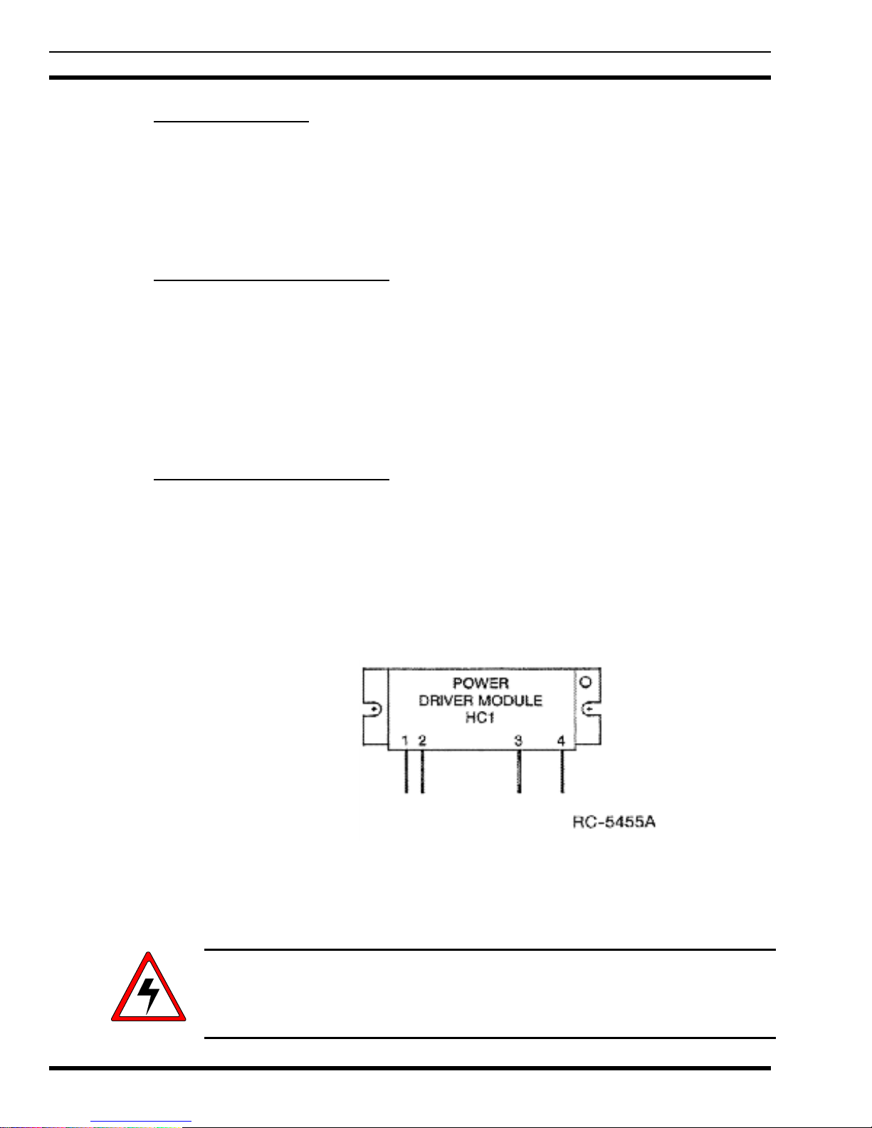
3.2 DRIVER REPLACEMENT
3.2.1 To Remove Driver HC1
1. Remove the two screws securing HC1 to the printed wire board.
2. Unsolder the four (4) leads bridging HC1 to the printed board while lifting each lead
as they are unsoldered.
easily.
3. Gently lift up on the module, taking care not to damage the spacer under the module.
SERVICE NOTE: The module may stick to the printed board.
3.2.2 To Replace Driver HC1
SERVICE NOTE: These leads are soft and can be bent very
1. Position the module properly, aligning the screw holes and leads with the printed
board. Trim leads if necessary (see Figure 1).
2. Replace the two screws securing the driver to the printed board, using a moderate
torque of 5 inch-pounds.
3. Solder the four leads of driver HC1 to the printed board and ground strap.
Figure 1 - Driver Lead Identification
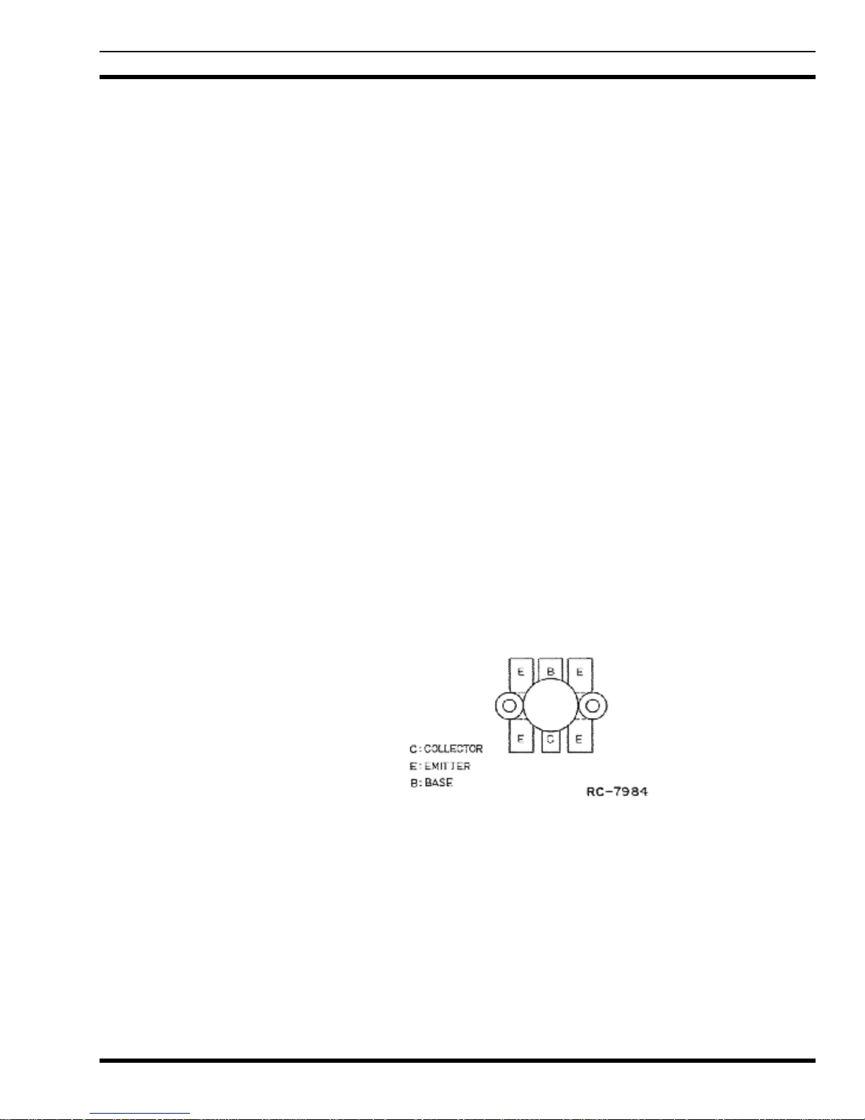
3.3 PA TRANSISTOR REPLACEMENT
The PA transistor contains Beryllium Oxide, a TOXIC substance. If the ceramic or
other encapsulation is opened, crushed, broken or abraded, the escaping dust may be
hazardous if inhaled. Use care when replacing the module.
WARNING
6
MAINTENANCE LBI-38425A
1. Remove the two retaining screws securing PA transistor TR1 to chassis assembly.
2. Unsolder and remove capacitors. Use a desoldering tool as necessary while lifting
the transistor leads with a small screwdriver or pick. Discard old capacitors.
3. Unsolder the emitter, base, and collector leads of the transistor, and remove it from
the printed board.
4. Remove all excess solder from the board, and clean the holes to allow the new
transistor to be positioned properly and the capacitors to fit into proper locations.
Refer to Figure 2 and trim the new transistor leads (if required) to the lead length of
the removed transistor.
5. Apply silicon grease to the back of the replacement transistor and place the transistor
into the mounting slot.
6. Replace the transistor mounting screws using a moderate torque of 5 inch-pounds.
7. Tack solder the four base leads to the printed board, using minimum solder. Then
solder the emitter and collector leads.
8. Install the capacitors into their proper mounting areas, flush to the board.
9. Solder the capacitor bodies to the printed board by first soldering the outside edge.
Then, holding the iron to the outside edge, touch the solder to the inside edge of the
capacitor. Be careful not to create solder bridges at the front and back edges of the
capacitors.
10. Remove any flux left on the board.
Figure 2 - PA Transistor Lead Identification
7
LBI-38425A MAINTENANCE
3.4 CHIP COMPONENT REPLACEMENT
Replacement of chip capacitors should always be done with a temperature controlled
soldering iron, using a controlled temperature of 700°F (371°C). However, DO NOT
touch black metal film of the resistors or the ceramic body of capacitors with the
soldering iron.
The metallized end terminations of the parts may be touched with the soldering iron
without causing damage.
NOTE
3.4.1 To Remove Chip Components
1. Using two soldering irons, heat each end of the chip at the same time until solder
flows and then remove and discard the chip.
2. Remove excess solder with a vacuum solder extractor.
3. Carefully remove the epoxy adhesive and excess flux to prevent damage to the
printed board.
3.4.2 To Replace Chip Components
1. Using as little solder as possible, “tin” one end of the component and one of the pads
on the printed wiring board.
2. Place the “tinned” end of the component on the “tinned” pad on the board and
simultaneously touch the component and the pad with a well “tinned” soldering iron
while pressing the component down on the board.
3. Place the “tinned” soldering iron on the other end of the component and the pad
simultaneously. Apply solder to the top of the end of the component until the solder
starts to flow. Use as little solder as possible while getting a good joint.
4. After the component has cooled, remove all flux from the component and printed
wiring board area with alcohol.
The CMOS integrated Circuit devices used in this equipment can be destroyed by static
discharges. Before handling one of these devices, the serviceman should discharge
himself by touching the case of a bench test instrument that has a 3-prong power cord
connected to an outlet with a known good earth ground. When soldering or desoldering
h
a CMOS device, the soldering iron should also have a 3-prong power cord connected to
an outlet with a known good earth ground. A battery-operated soldering iron may be
used in place of the regular soldering iron.
8

DISASSEMBLY PROCEDURE LBI-38425A
4 DISASSEMBLY PROCEDURE
4.1 TO REMOVE THE SYSTEM CONTROL/SYNTHESIZER BOARD
1. Remove the two (2) screws ! securing the top cover (refer to Figure 3). Remove the
top cover. Then disconnect the interconnecting cables.
2. Remove the eight (8) screws " securing the Synthesizer shield. Remove the shield.
3. Remove the three (3) screws # securing the board.
4. Remove the screws $ securing regulator and carefully lift up and remove the board.
Figure 3 – Disassembly Procedure (Top View)
9
 Loading...