

Page 1
Freescale Semiconductor
Technical Data
REFERENCE DESIGN IN 1st REVIEW -- 06/03/11
Available at http://www.freescale.com. Go to Support/Software & Tools/
Additional Resources/Reference Designs/Networking
Rev . 1.1, 6/2011
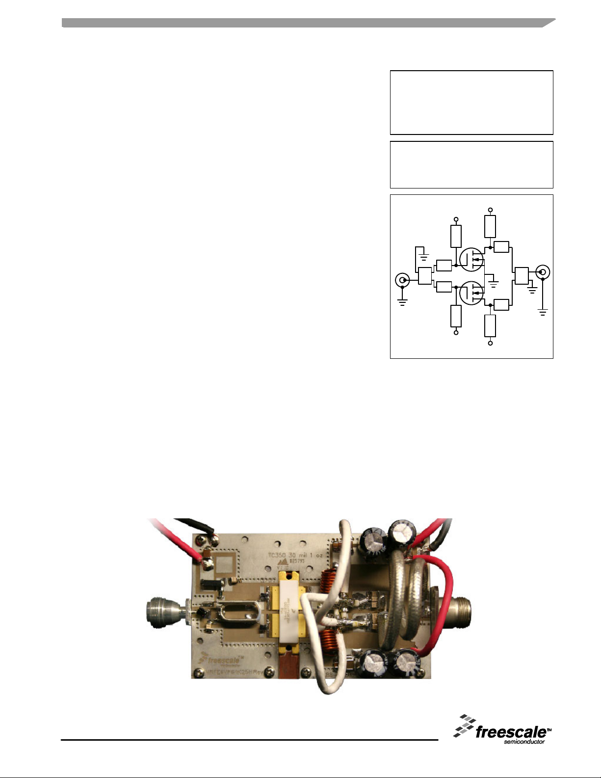
RF Power Reference Design Library
FM Broadcast Reference Design
High Ruggedness N--Channel Enhancement--Mode
Lateral MOSFETs
Reference Design Characteristics
The MRFE6VP61K25H/HS are versatile devices and are well suited for a
wide range of applications. They are capable of delivering 1.2 kW under
continuous wave test signaling as a result of their high efficiency and low
thermal resistance. This document focuses on FM broadcast radio applications
for both analog and complex modulation waveforms.
Frequency Band: 87.5--108 MHz
Output Power: 1100 Watts CW
Supply Voltage: 50 Vdc
Power Gain (Typ): 25 dB
Drain Efficiency (Min): 79% (at fundamental frequency)
The MRFE6VP61K25H/HS products are enhanced ruggedness 50 volt
LDMOS power transistors that can operate in harsh environments and in highly
mismatched applications (within the limit of maximum junction temperature).
These parts are designed for high voltage operation and are fabricated using
Freescale’s very high voltage 6th generation (VHV6E) platform.
MRFE6VP61K25H
MRFE6VP61K25HS
FM Broadcast
87.5--108 MHz, 1100 W CW, 50 V
FM BROADCAST
REFERENCE DESIGN
V
DD
BIAS
M
OUTPUT
+
-
M
BIAS
V
DD
RF
INPUT
M=Match
V
GG
BIAS
M
+
M
BIAS
V
GG
RF
FM BROADCAST REFERENCE DESIGN
This reference design is designed to demonstrate the RF
performance characteristics of the MRFE6VP61K25H/HS
devices when applied to the 87.5--108 MHz FM broadcast
frequency band. The reference design is tuned for
performance at 1100 watts CW output power, V
and IDQ= 200 mA.
=50volts
DD
REFERENCE DESIGN LIBRARY TERMS
AND CONDITIONS
Freescale is pleased to make this reference design
available for your use in development and testing of your
own product or products. The reference design contains an
easy--to--copy, fully functional amplifier design. It consists of
“no tune” distributed element matching circuits designed to
be as small as possible, and is designed to be used as a
“building block” by our customers.
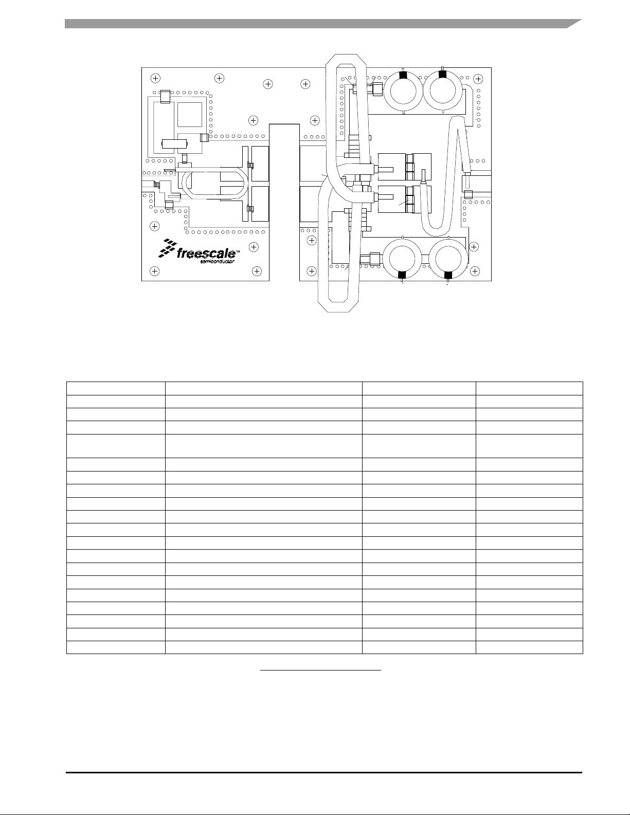
HEATSINKING
When operating this fixture it is critical that adequate heatsinking is provided for the device. Excessive heating of the
device may prevent duplication of the included measurements
and/or destruction of the device.
Figure 1. FM Broadcast Reference Design Fixture
Freescale Semiconductor, Inc., 2011.All rights reserved.
RF Reference Design Data
Freescale Semiconductor
MRFE6VP61K25H MRFE6VP61K25HS FM Broadcast
1
Page 2
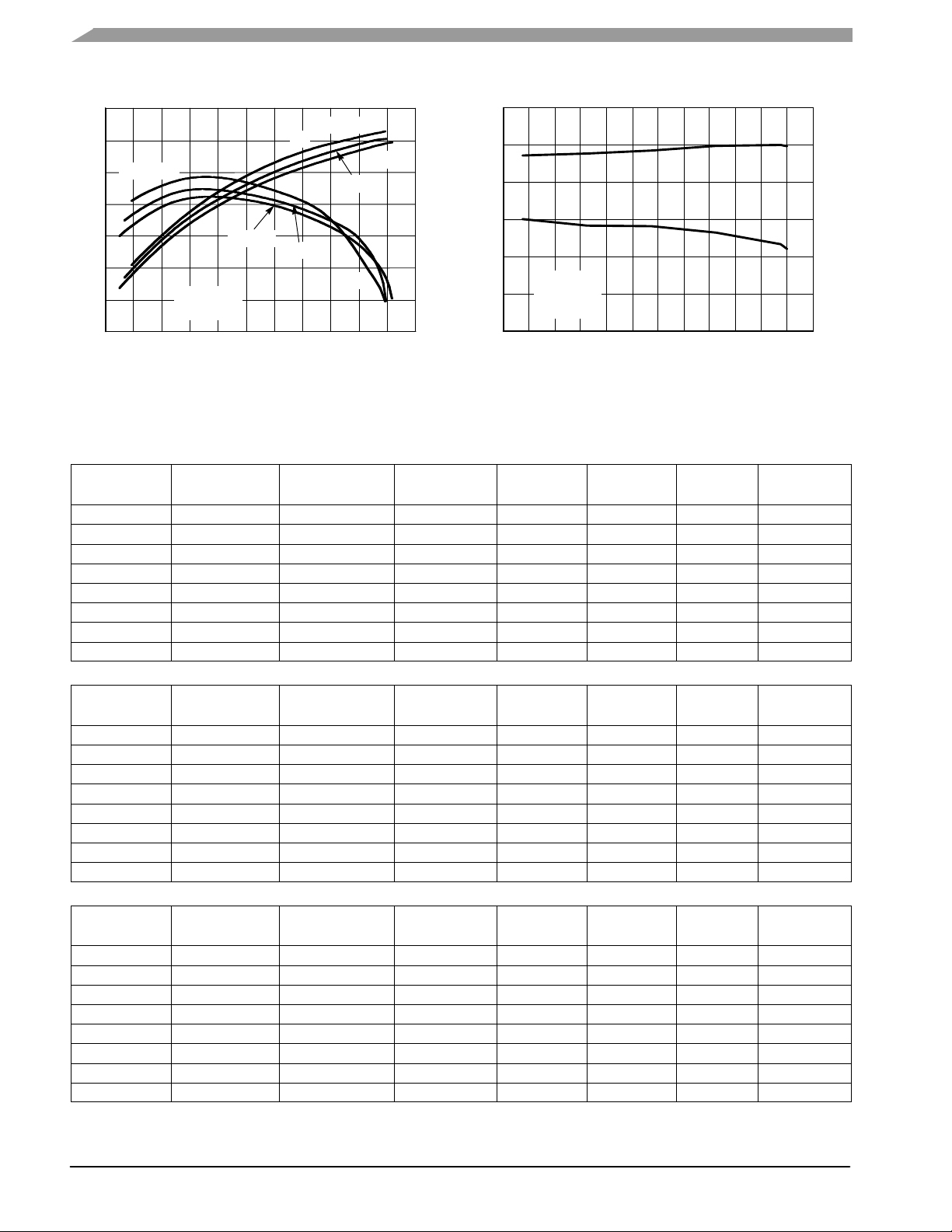
MEASUREMENTS
31
30
29
28
f = 108 MHz
108 MHz
D
87.5 MHz
98 MHz
90
80
70
32
30
D
28
60
26
27
, POWER GAIN (dB)
ps
26
G
25
VDD=50V
I
DQ
= 200 mA
87.5 MHz
98 MHz
G
ps
24
300 500 700 1100
200 400 600 800 900 1000
100
, OUTPUT POWER (WATTS)
P
out
Air--Cooled, CW, 87.5--108 MHz, Low Pass Filter
Figure 2. Continuous Wave Performance Graph
with Low Pass Filter versus Output Power
1200
50
24
, POWER GAIN (dB)
DRAIN EFFICIENCY (%)
40
30
20
ps
G
D,
22
P
out
V
DD
I
DQ
= 1100 W
=50V
= 200 mA
20
88 92 96 100 102 104
86
G
ps
f, FREQUENCY (MHz)
Air--Cooled, CW, 87.5--108 MHz, Low Pass Filter
Figure 3. Continuous Wave Performance Graph
with Low Pass Filter versus Frequency
Table 1. CW Drive--Up at 87.5 MHz
P
in
(W)
0.3 150 27.0 -- 6 . 1 33.6 50 8.9 0.2
0.5 314 28.0 -- 6 . 5 48.0 50 13.1 0.2
1.0 639 28.1 -- 8 . 1 65.8 50 19.4 0.2
1.5 844 27.5 -- 10.1 72.6 50 23.2 0.2
2.0 975 26.9 -- 1 1 . 9 76.1 50 25.6 0.2
2.5 1056 26.3 --13.0 78.1 50 27.0 0.2
3.0 1100 25.6 --13.3 79.1 50 27.8 0.2
3.5 111 6 25.0 -- 13.6 79.2 50 28.2 0.2
P
(W)
out
Gain
(dB)
IRL
(dB)
Eff
(%)
V
(V)
DD
I
(A)
Table 2. CW Drive--Up at 98 MHz
P
in
(W)
0.3 168 27.5 -- 1 1 . 0 36.8 50 9.1 0.2
0.5 343 28.4 -- 1 1 . 8 52.0 50 13.2 0.2
1.0 660 28.2 -- 14.9 68.5 50 19.3 0.2
1.5 864 27.6 -- 19.4 75.3 50 22.9 0.2
2.0 999 27.0 -- 22.4 78.7 50 25.4 0.2
2.5 1058 26.3 --22.0 80.1 50 26.4 0.2
3.0 1085 25.6 --22.0 80.2 50 27.0 0.2
3.5 1094 24.9 --22.6 80.4 50 27.2 0.2
P
(W)
out
Gain
(dB)
IRL
(dB)
Eff
(%)
V
(V)
DD
I
(A)
Table 3. CW Drive--Up at 108 MHz
P
in
(W)
0.3 193 28.1 -- 14.2 40.9 50 9.4 0.2
0.5 377 28.8 -- 14.9 56.1 50 13.4 0.2
1.0 695 28.4 -- 15.6 72.9 50 19.1 0.2
1.5 881 27.7 -- 13.5 78.6 50 22.4 0.2
2.0 980 26.7 -- 14.1 79.2 50 22.9 0.2
2.5 1018 26.1 --12.2 81.6 50 24.9 0.2
3.0 1066 25.5 -- 11 . 8 82.4 50 25.9 0.2
3.5 1092 24.9 -- 11 . 8 82.7 50 26.4 0.2
1. IDQis set by adjusting a variable gate--source voltage while maintaining a constant 50 volts at the drain.
P
(W)
out
Gain
(dB)
IRL
(dB)
Eff
(%)
V
(V)
DD
I
(A)
DD
DD
DD
108
90
80
70
60
50
DRAIN EFFICIENCY (%)
D,
40
30
11090 94 98 106
(1)
I
DQ
(A)
(1)
I
DQ
(A)
(1)
I
DQ
(A)
MRFE6VP61K25H MRFE6VP61K25HS FM Broadcast
2
RF Reference Design Data
Freescale Semiconductor
Page 3
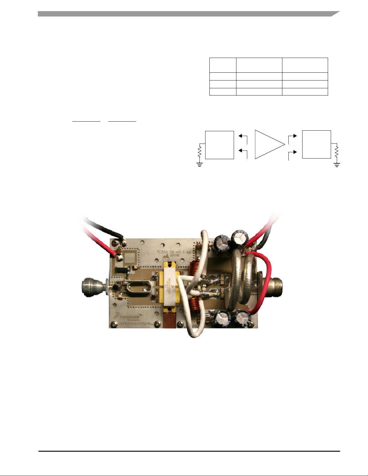
AMPLIFIER DESIGN
MATCHING NETWORK
As a first order approximation, the typical maximum
efficiency impedance point corresponds to a 25% power
degradation from the maximum P3dB impedance. The
maximum output power impedance value on this device
corresponds to a 1.25 kW output capability from
87.5--108 MHz. This puts the targeted P1dB compression
value at 800 watts of output power total, or 400 watts per
side. The initial load impedance is determined using the
following equation:
out
2
=
)
(0.85 50 V)
(2 400 W)
(0.85 VDD)
R=
(2 P
R (drain to drain) = 2.25 x2=4.5
The coaxial transformer turns ratio was chosen to meet
this required impedance level and the length of the coax
(series inductance) was tuned to attain maximum efficiency
and maximum power transfer between the device and its
complex conjugate test fixture load impedance.
2
=2.25
FIXTURE IMPEDANCE
VDD=50Vdc,IDQ= 200 mA, P
f
MHz
87.5 2.20 + j6.70 4.90 + j2.90
98 2.30 + j6.90 4.10 + j2.50
108 2.30 + j7.00 4.40 + j3.60
Z
= Test circuit impedance as measured from
source
= Test circuit impedance as measured from
Z
load
Input
Matching
Network
Z
source
gate to gate, balanced configuration.
drain to drain, balanced configuration.
Device
Under
+
Tes t
-- +
Z
source
Figure 4. Series Equivalent Source and Load
Impedance
= 1100 W CW
out
--
Z
load
Z
load
Output
Matching
Network
RF Reference Design Data
Freescale Semiconductor
Figure 5. FM Broadcast Reference Design Fixture Impedance
MRFE6VP61K25H MRFE6VP61K25HS FM Broadcast
3
Page 4
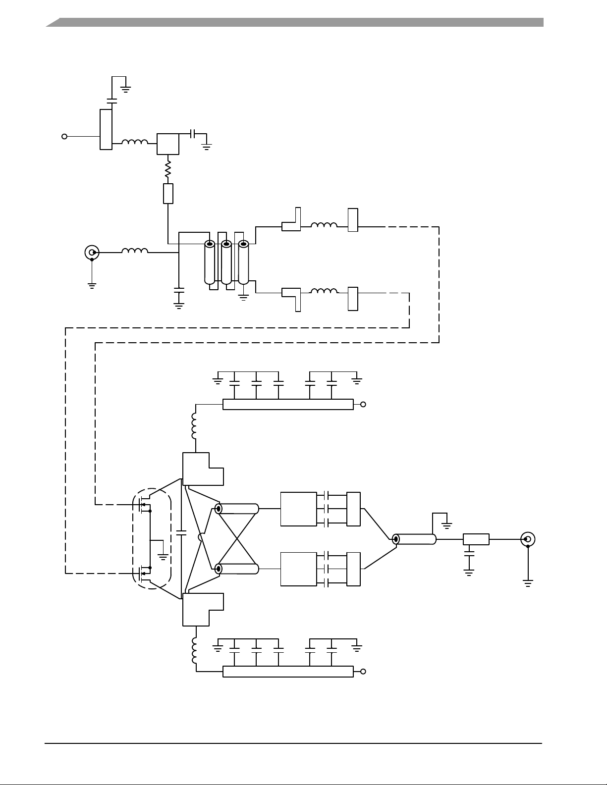
CIRCUIT DESCRIPTION
C1
C3
V
GS
B1
R1
RF
INPUT
T1
L1
C2
C15 C16 C17 C19 C18
B2
COAX1
C4
L2
L3
V
DD
C7
C8
C9
COAX3
RF
OUTPUT
COAX2
B3
C22 C23 C24 C21 C20
Figure 6. FM Broadcast Reference Design Schematic Diagram
MRFE6VP61K25H MRFE6VP61K25HS FM Broadcast
4
C10
C11
C12
C5
V
DD
RF Reference Design Data
Freescale Semiconductor
Page 5
C1
COAX1
C15
C16
C17
C19 C18
+
+
B1
C3
R1
L1
C2
MRFE6VP61K25H Rev. 1
Note: Component numbers C6, C13 and
C14 are not used.
T1
L2
L3
CUT OUT AREA
C4
L4
L5
C22
COAX2
C11
C24
C23
COAX3
C7
C8
C9
C10
C12
+
C21 C20
C5
+
Figure 7. FM Broadcast Reference Design Component Layout
Table 4. FM Broadcast Reference Design Component Designations and Values
Part Description Part Number Manufacturer
B1 Long Ferrite Bead 2743021447 Fair--Rite
C1
C2 27 pF Chip Capacitor ATC100B270JT500XT ATC
C3, C7, C8, C9, C10,
C11, C12
C4 39 pF Mica Capacitor MIN02--002DC390J--F Cornell Dubilier
C5 3 pF Chip Capacitor ATC100B3R0CT500XT ATC
C15, C22 10K pF Chip Capacitors ATC200B103KT500XT ATC
C16, C23 1 F, 100 V Chip Capacitors C3225JB2A105KT TDK
C17, C24 10 F, 100 V Chip Capacitors C5750X7S2A106MT TDK
C18, C19, C20, C21 470 F, 63 V Electrolytic Capacitors 477KXM063M Illinois Capacitor
L1 39 nH Inductor 1812SMS--39NJLC Coilcraft
L2, L3 2.5 nH Inductors A01TKLC Coilcraft
L4, L5 7 Turn, #16 AWG, ID = 0.3 Inductors Copper Wire
R1 11 , 1/4 W Chip Resistor CRCW120611R0FKEA Vishay
T1 Balun TUI--9 Comm Concepts
Coax1, Coax2 Flex Cables, 12 ,5.9 TC--12 Comm Concepts
Coax3 Coax Cable, Quickform 50 ,8.7 SUCOFORM 250--01 Huber+Suhner
PCB* 0.030, r=3.5 TC--350 Arlon
Heatsink NI--1230 Copper Heatsink C193X280T970 Machine Shop
6.8 F, 50 V Chip Capacitor C4532X7R1H685K TDK
1000 pF Chip Capacitors ATC100B102JT50XT ATC
*PCB artwork for this reference design is available at http://freescale.com/RFbroadcast > Design Support > Reference Designs.
Note: See Appendix A for Tuning Tips.
MRFE6VP61K25H MRFE6VP61K25HS FM Broadcast
RF Reference Design Data
Freescale Semiconductor
5
Page 6

FREESCALE RF POWER 50 V TECHNICAL ADVANTAGES
50 V Drain Voltage
The 87.5--108 MHz FM broadcast reference design fixture
was designed to utilize the standard 50 volt power supply
commonly used in this market.
Data was collected to characterize the reference design’s
output power and efficiency vs. drain voltage, as shown in
Figure 8. The output power can be adjusted over a 12 dB
worth of dynamic range by adjusting the drain voltage, while
creating minimal degradation on the efficiency performance.
Refer to Freescale’s 50 V RF LDMOS White Paper.Goto
http://freescale.com/RFpower
and select Documentation/White Papers -- 50VRFLDMOSWP for more information
on 50 V RF LDMOS technology.
1200
1000
, OUTPUT POWER (WATTS)
out
P
800
600
400
200
0
Pin=3.5W
f=98MHz
I
= 200 mA
DQ
10
D
P
out
20 30 40 50515253545
V
, DRAIN VOLTAGE (VOLTS)
DD
90
85
80
75
70
65
60
55
Figure 8. Output Power and Drain Efficiency
versus Drain Voltage
Extended Gate Voltage Range
The enhanced electrostatic discharge (ESD) protection
structure at the gate of the transistor is a Freescale
innovation pioneered in the cellular infrastructure market that
is incorporated into the 50 volts RF LDMOS power product
portfolios. This ESD structure can tolerate moderate reverse
bias conditions, applied to the gate lead, up to --6 volts as
shown in Figure 9. This allows these transistors to be used in
zero gate voltage, Class C bias applications where the RF
voltage swings on the gate can be significantly lower than the
ground potential.
2.E--02
1.E--02
5.E--03
(A)
0.E+00
ESD
I
-- 5 . E -- 0 3
-- 1 . E -- 0 2
-- 2 . E -- 0 2
-- 1 5 0--10 --5 5 10 15 20 25
2.E--02
1.E--02
5.E--03
(A)
0.E+00
ESD
I
-- 5 . E -- 0 3
-- 1 . E -- 0 2
-- 2 . E -- 0 2
-- 1 5 0--10 --5 5 10 15 20 25
Enhanced ESD
V
(V)
GS
Standard ESD
V
(V)
GS
Figure 9. Gate Voltage Breakdown with ESD
DRAIN EFFICIENCY (%)
D,
High Ruggedness/Energy Absorption
The MRFE6VP61K25H/HS was designed to operate in
applications which demand very high ruggedness. The
VHV6E technology has proven to be valuable in FM broadcast applications, specifically in high definition (HD) FM
transmitters where a high peak--to--average (PAR) digital signal is injected on top of an existing analog FM signal. At the
peak of the signal, the voltage waveform could exceed the
V
(BR)DSS
the device to enter into an avalanche condition. However, for
the device to fail, the current must be sufficiently high enough
during the high voltage period to activate the internal parasitic bipolar transistor buried beneath the active field--effect
transistor (FET) structure.
An Integrated Technologies Corporation’s Unclamped
Inductive Load Tester, model #ITC55100B, was used to
measure the maximum energy dissipation capability of the
device under these high current and high voltage test
conditions.
breakdown voltage of the device and thus cause
MRFE6VP61K25H MRFE6VP61K25HS FM Broadcast
6
RF Reference Design Data
Freescale Semiconductor
Page 7

Figure 10 shows the internal diagram of the ITC55100B
tester. The tester controller activates the pulse generator to
turn on the device under test (DUT) through the limiting and
terminating resistor, R
, creating a very clean gate pulse
G
waveform. This pulse waveform tests the maximum energy
dissipation capability of the DUT by stressing it under
various, controlled energy levels. This is accomplished by
attaching an unclamped inductive load to the device’s drain
and source connection and then increasing both the load
current and load voltage up until the point that the DUT
Controller
Measurement
Pulse
Generator
Kelvin
Isolator
50
R
50
R
G
G
failure is achieved. Using this test method for power devices
ensures proper operation in circuits used to drive inductive
loads that may possibly cause an avalanche mode stress on
the DUT. The final maximum energy dissipation capability
rating, in joules, is calculated by the following equation:
E=
1
2
L I
2
where L is the load inductance value and I is the peak current
within the load inductor.
L
D
I
D
Monitor
DUT
High Speed
Switch
Freewheeling
Diode
+
V
D
--
Figure 10. Internal Diagram of the ITC55100B Tester
The highest energy level the MRFE6VP61K25H/HS
device passed is shown in Figure 11. During the course of
this testing, the device dissipated over 5.77 joules of energy
over a discharge time of 859 sec, while reaching a
maximum current of 76 A and a maximum voltage of
197 volts. (These load voltage and current values are taken
under short discharge durations to keep the thermal
dissipation issues out of the ruggedness equation.)
Max Voltage = 196.8 Vdc
End Voltage = 167.5 Vdc
Energy = 5.766 J (full device)
ID
peak
=76A
RF Reference Design Data
Freescale Semiconductor
Figure 11. Voltage and Current Curves During Energy Discharge
MRFE6VP61K25H MRFE6VP61K25HS FM Broadcast
7
Page 8

Reliability
Mean time to failure (MTTF) is defined as a 10% reduction
in current handling capability on 50% of the devices within a
given sample size. The primary factor in device failure is due
to metal electromigration on the die surface. Once the
average operating conditions for a given application are
determined, then the MTTF can be calculated using the
thermal resistance R
product data sheet.
Example: If the desired operating output power is 1100 W,
with 80% drain efficiency.
I
= 1100 W / (80% 50 V) ~ 27.5 A
Drain
MRFE6VP61K25H Rth=0.15C/W, case temperature =
80C
Dissipated power = P
Dissipated power = 50 V 27.5 A -- 1100 W + 4 W = 279 W
Temperature rise = 279 W 0.15C/W = 42C
T
J=Trise+TC
Utilizing Figure 12 which calculates MTTF versus I
and TJ;I
100000
10000
1000
= 27.5 A, MTTF for this example is 2700 years.
Drain
32 Amp
value given in the MRFE6VP61K25H
th
-- P
dc
out+Pin
=42C+80C = 122C
24 Amp
Drain
87.5 MHz, 1100 W CW, 79% Drain Efficiency
100
MTTF (YEARS)
10
1
90
110 130 150 170 190
28 Amp
T
, JUNCTION TEMPERATURE (C)
J
210 230
250
Figure 12. MTTF versus Junction Temperature
THERMAL MEASUREMENTS
Thermal images of the MRFE6VP61K25H FM broadcast
reference circuit were taken using a FLIR Infrared(IR) T360
camera. The hottest point observed was located at the
Coax1 and Coax2 junction point with the C4 mica capacitor
at 108 MHz. The recorded temperature was 100C after
10 minutes of operation to reach steady state temperature.
Due to the high efficiency achieved by the FM broadcast
reference fixture, the overall baseplate temperature remains
relatively cool at around 60C, with forced air cooling at
25C.
98 MHz, 1100 W CW, 78% Drain Efficiency
108 MHz, 1100 W CW, 80% Drain Efficiency
Figure 13. IR Images of the Output Matching Network
MRFE6VP61K25H MRFE6VP61K25HS FM Broadcast
8
RF Reference Design Data
Freescale Semiconductor
Page 9

APPENDIX A
Tuning Tips
Increasing C4 increases efficiency at the low end of the
band (87.5 MHz), but there is a trade--off in power at the
high end of the band.
Increasing the length of Coax3 increases efficiency at the
low end of the band (87.5 MHz), but there is a trade off in
efficiency and power at the high end of the band.
Make sure all the coax are measured tip to tip.
Increasing C5 increases the power, but lowers efficiency.
RF Reference Design Data
Freescale Semiconductor
MRFE6VP61K25H MRFE6VP61K25HS FM Broadcast
9
Page 10

APPENDIX B
Mounting Tips
The MRFE6VP61K25H/HS is packaged in the industry
standard NI--1230 air cavity package which offers a standardized package for easy replacement drop in as well as
outstanding thermal performance.
This package can be assembled into a power amplifier
system using several different mounting methods. The
popular options include bolting down with screw, clamping
and reflow soldering in a cavity. Freescale recommends
solder reflow. If customer desires to clamp the device,
special care needs to be taken due to cavity style packages.
One of the key advantages to solder mounting includes a
superior source contact--to--heatsink interface that provides
for lower thermal resistance as well as better electrical
grounding, which means that high power RF devices such as
the MRFE6VP61K25H/HS parts will have a lower junction
temperature and better RF performance when compared to
all other mounting options. Lowering the junction
temperature of the device also increase the MTTF (Mean
Time to Failure), as shown in Figure 8, MTTF versus
Junction Temperature.
Refer to AN1908 Solder Reflow Attach Method for High
Power RF Devices in Air Cavity Packages.Goto
http://freescale.com/RFpower
Application Notes -- AN1908 for more information on solder
reflow attach method.
and select Documentation/
MRFE6VP61K25H MRFE6VP61K25HS FM Broadcast
10
RF Reference Design Data
Freescale Semiconductor
Page 11

APPENDIX C
RF Bench Setup/Continuous Wave Performance (CW)
PinN1912
Channel A
with
10 dB Attenuator
Narda Model 31993
50--1000 MHz Coupler
Power Reflected
HP437
with
10 dB Attenuator
V
GG
DUTESG Generator
Figure 14. RF Bench Setup
V
DD
Tenuline Coaxial
Attenuator
Model (8329--300)
30 dB Attenuator
+19 dB additional
DC to 3 GHz
150 MHz
LPF
Power Meter
N1912
Channel B
RF Reference Design Data
Freescale Semiconductor
MRFE6VP61K25H MRFE6VP61K25HS FM Broadcast
11
Page 12

APPENDIX D
Copper Heatsink for FM Broadcast Fixture
8x
#4--40
0.300 deep
2.737 (69.51)
1.929 (48.98)
0.41 (10.41)
4.548 (115.52)
2.882 (73.19)
2.719 (69.07)
D
D
A
B
A
1.813 (46.04)
0.813 (20.64)
0.140 (3.56)
0.125 (3.17)
0.000 (0.00)
0.00 (0.00)
0.177 (4.50)
E
F
E
F
0.929 (23.59)
1.558 (39.58)
1.724 (43.78)
2.134 (54.19)
1.929 (48.99)
0.038 (0.97)
EE
2.929 (74.38)
2.283 (57.98)
C, Device Channel
D
A
A
D
B
4.499 (114.28)
4.725 (120.02)
AA
0.300 (7.62)
0.720 (18.29)
2.011 (51.08)
1.309 (33.26)
0.611 (15.52)
0.130 (3.32)
0.000 (0.00)
0 (0.00)
D
A
B
A
0.000 (0.00)
0.128 (3.25)
1.668 (42.38)
1.489 (37.83)
0.188 (4.76)
1.129 (28.69)
0.950 (24.14)
D
0.324 (8.23)
inches (mm)
Gutter is 0.030 wide
and 0.046 deep, both
0.929 (23.59)
sides
0.720 Copper Heatsink Hole Details
Designators
A 2 places, both sides, drill and tap, #2--56 screw depth 0.300
B 2 places, both sides, 0.1875 diameter notch 0.020 deep
C NI--1230 channel 0.410 wide by 0.0380 deep
D 2 places, both sides, drill depth 0.250 and tap for #4--40 screw
E Locator holes from bottom diameter = 0.257, depth = 0.400
F 2 places, drill through and tap for #4--40 screw
Figure 15. NI--1230 Heatsink
MRFE6VP61K25H MRFE6VP61K25HS FM Broadcast
12
2.929 (74.39)
Details
RF Reference Design Data
Freescale Semiconductor
Page 13

REVISION HISTORY
The following table summarizes revisions to this document.
Revision Date Description
1 May 2011 Table 4, Component Designations and Values, updated C17, C24 capacitor from “50 V,
1.1 June 2011 Content flow restructured
GRM55DR61H106KA88L, Murata” to “100 V, C5750X7S2A106MT, TDK”, 100 V part provides higher
breakdown voltage capability. Corrected R1 part number from “CRCW1206110FKEA” to
CRCW120611R0FKEA”. For Coax1, 2, 3, in description changed cm to inches, p. 4.
RF Reference Design Data
Freescale Semiconductor
MRFE6VP61K25H MRFE6VP61K25HS FM Broadcast
13
Page 14

How to Reach Us:
Home Page:
www.freescale.com
Web Support:
http://www.freescale.com/support
USA/Europe or Locations Not Listed:
Freescale Semiconductor, Inc.
Technical Information Center, EL516
2100 East Elliot Road
Tempe, Arizona 85284
1--800--521--6274 or +1--480--768--2130
www.freescale.com/support
Europe, Middle East, and Africa:
Freescale Halbleiter Deutschland GmbH
Technical Information Center
Schatzbogen 7
81829 Muenchen, Germany
+44 1296 380 456 (English)
+46 8 52200080 (English)
+49 89 92103 559 (German)
+33169354848(French)
www.freescale.com/support
Japan:
Freescale Semiconductor Japan Ltd.
Headquarters
ARCO Tower 15F
1--8--1, Shimo--M eguro, Meguro--ku,
Tokyo 153--0064
Japan
0120 191014 or +81 3 5437 9125
support.japan@freescale.com
Asia/Pacific:
Freescale Semiconductor China Ltd.
Exchange Building 23F
No. 118 Jianguo Road
Chaoyang District
Beijing 100022
China
+86 10 5879 8000
support.asia@freescale.com
For Literature Requests Only:
Freescale Semiconductor Literature Distribution Center
1--800--441--2447 or +1--303--675--2140
Fax: +1--303--675--2150
LDCForFreescaleSemiconductor@hibbertgroup.com
Information in this document is provided solely to enable system and software
implementers to use Freescale Semiconductor products. There are no express or
implied copyright licenses granted hereunder to design or fabricate any integrated
circuits or integrated circuits based on the information in this document.
Freescale Semiconductor reserves the right to make changes without further notice to
any products herein. Freescale Semiconductor makes no warranty, representation or
guarantee regarding the suitability of its products for any particular purpose, nor does
Freescale Semiconductor assume any liability arising out of the application or use of
any product or circuit, and specifically disclaims any and all liability, including without
limitation consequential or incidental damages. “Typical” parameters that may be
provided in Freescale Semiconductor data sheets and/or specifications can and do
vary in different applications and actual performance may vary over time. All operating
parameters, including “Typicals”, must be validated for each customer application by
customer’s technical experts. Freescale Semiconductor does not convey any license
under its patent rights nor the rights of others. Freescale Semiconductor products are
not designed, intended, or authorized for use as components in systems intended for
surgical implant into the body, or other applications intended to support or sustain life,
or for any other application in which the failure of the Freescale Semiconductor product
could create a situation where personal injury or death may occur . Should Buyer
purchase or use Freescale Semiconductor products for any such unintended or
unauthorized application, Buyer shall indemnify and hold Freescale Semiconductor
and its officers, employees, subsidiaries, affiliates, and distributors harmless against all
claims, costs, damages, and expenses, and reasonable attorney fees arising out of,
directly or indirectly, any claim of personal injury or death associated with such
unintended or unauthorized use, even if such claim alleges that Freescale
Semiconductor was negligent regarding the design or manufacture of the part.
Freescalet and the Freescale logo are trademarks of Freescale Semiconductor, Inc.
All other product or service names are the property of their respective owners.
Freescale Semiconductor, Inc. 2011. All rights reserved.
MRFE6VP61K25H MRFE6VP61K25HS FM Broadcast
Available at http://www.freescale.com. Go to Support/Software & Tools/
Additional Resources/Reference Designs/Networking
14
Rev. 1.1, 6/2011
RF Reference Design Data
Freescale Semiconductor
 Loading...