

Page 1
r
^ \
r
SERVICE MANUAL
PC50-II
OCTOBER, 1989
____________________
PN-314034-01
_______
J
J
C= Commodore
Page 2

Page 3
SERVICE MANUAL
PC50-II
OCTOBER, 1989 PN-314034-01
Reprinted with permission of
mitac
’ International Corporation
All rights reserved.
CBM INTER-COMPANY
(NOT FOR RESALE)
Commodore Business Machines, Inc.
1200 Wilson Drive, West Chester, Pennsylvania 19380 U.S.A.
Commodore makes no expressed or implied war
ranties with regard to the information contained
herein. The information is made available solely on
an as is basis, and the entire risk as to quality and
accuracy is with the user. Commodore shall not be
liable for any consequential or incidental damages
in connection with the use of the information con
tained herein. The listing of any available replace
ment part herein does not constitute in any case
a recommendation, warranty or guaranty as to
quality or suitability of such replacement part.
Reproduction or use without expressed permission,
of editorial or pictorial content, in any matter is
prohibited.
This manual contains copyrighted and proprietary information. No part
of this publication may be reproduced, stored in a retrieval system, or
transmitted in any form or by any means, electronic, mechanical,
photocopying, recording or otherwise, without the prior written permis
sion of Commodore Electronics Limited.
Copyright © 1989 by Commodore Electronics Limited.
All rights reserved.
Page 4

Page 5
PC50-III SERVICE MANUAL
NOTICE
The following trademarks are the respective properties of the following trademark holders:
IBM, PC/AT, PS/2, PC-DOS, OS/2, IBM VGA
Trademarks of International Business Machines Corp.
MS-DOS, XENIX
Trademarks of Microsoft Corp.
Intel
Trademark of Intel Corp.
Lotus
Trademark of Lotus Development Corp.
C-DOS
Trademark of Digital Research, Inc.
Novell NetWare
Trademark of Novell, Inc.
Hercules
Trademark of Hercules Computer Technology
Paradise
Trademark of Paradise System, Inc.
Page 6

Page 7

PC50-III SERVICE MANUAL
PREFACE
This manual is intended to help you isolate and correct problems with your system. It is
divided into the following sections:
Chapter 1, General Information, provides a general description and specifications for your
system.
Chapter 2, Theory of Operations, provides the theory of operation and information on the
system board.
Chapter 3, Hardware Interface, provides information on the system’s internal interfaces
such as jumper settings, connector definitions and their pin assignments.
Chapter 4, Removing Components, provides instructions for removing options.
Chapter 5, Diagnostics, provides information on diagnostic problems and POST proce
dures.
Chapter 6, Maintenance, provides the service diagrams and system components informa
tion.
Page 8

Page 9
PC50-II1 SERVICE MANUAL
TABLE OF CONTENTS
CHAPTER 1 GENERAL INFORMATION
1.1 Product Description....................................................................................................1-1
1.2 Feature Description..................................................................................................... 1-2
1.3 System Unit................................................................................................................... 1-3
1.4 Product Specification................................................................................................... 1-5
CHAPTER 2 THEORY OF OPERATION
2.1 System Components....................................................................................................2-1
2.2 System Operation...................................................................................................... 2-10
CHAPTER 3 HARDWARE INTERFACE
3.1 Jumper And Connector Definition............................................................................3-1
3.2 Analog Video Output Port Connector.......................................................................3-5
3.3 SIO Loopback Connector............................................................................................ 3-6
3.4 PIO Loopback Connector........................................................................................... 3-7
3.5 Keyboard Connector....................................................................................................3-8
3.6 Disk Drive.....................................................................................................................3-9
CHAPTER 4 REMOVING COMPONENTS
4.1 Removing System Unit Cover......................................................................................4-1
4.2 Removing An Option Board........................................................................................4-3
4.3 Removing Disk Drives.................................................................................................4-4
iii
Page 10
PC50-III SERVICE MANUAL
4.4 Removing DRAM Modules........................................................................................4-8
4.5 Removing Numeric Coprocessor
...............................................................................
4-9
4.6 Removing Power Supply............................................................................................4-11
4.7 Removing System Board...........................................................................................4-12
CHAPTERS DIAGNOSTICS
5.1 Diagnostics Program................................................................................................... 5-1
5.2 Power-On Self Test................................................................................................... 5-15
CHAPTER 6 MAINTENANCE
6.1 Main Components Information................................................................................... 6-1
6.2 Service Diagrams......................................................................................................... 6-2
iv
Page 11
PC50-III SERVICE MANUAL
LIST OF FIGURES
Figure 1-1. Front View of the System Unit
Figure 1-2. Rear View of the System Unit........................................................................ 1-4
Figure 2-1. System Block Diagram....................................................................................2-2
Figure 2-2. PVGA1 Functional Block Diagram
Figure 2-3. Clock Selection Block Diagram
Figure 2-4. DRAM Organization.................................................................................... 2-13
Figure 2-5. DRAM Interleaved Operation.....................................................................2-15
Figure 2-6. DRAM Page Mode Operation.....................................................................2-17
Figure 2-7. DRAM Page/Interleave Operation
Figure 2-8. System RAM/ROM Mapping For 1MB System RAM...............................2-18
Figure 2-11. EMS Mapping............................................................................................... 2-20
Figure 2-12. Page/Interleaved Mode, Read After Write, OW.S
Figure 2-13. Page/Interleaved Mode, Write Cycle With RAS Being Inactive 0 W.S. ...2-22
Figure 2-14. Page/Interleaved Mode, Read Cycle With RAS Being Inactive 0 W.S
Figure 2-15. Block Diagram For DRAM Access............................................................. 2-24
Figure 2-16. EPROM Read Cycle.....................................................................................2-25
Figure 2-17. Block Diagram For EPROM Access
.......................................................................
...............................................................
................
.............................................................
2-11
......................................
....
...........................................................
1-3
2-5
2-17
2-21
2-23
2-26
Figure 2-18. Bus Conversion Data Paths...........................................................................2-28
Figure 2-19. Normal Mode Local Cycle Followed By AT Bus Cycle (Ows, Ocd)
Figure 2-20. Normal Mode AT Bus Cycle With Additinal Hold Time(0ws,0cd)
Figure 2-21. Delayed Mode AT Bus Cycle (3ws, 2cd).....................................................2-33
Figure 2-22. Refresh/DMA Sequence
Figure 2-23. DMA Cycle Sequence...................................................................................2-36
Figure 2-24. PO RTB .........................................................................................................2-38
Figure 3-1. System Board Jumpers And Connectors.......................................................3-4
..............................................................................
...........
..........
2-31
2-32
2-35
v
Page 12
PC50-III SERVICE MANUAL
LIST OF TABLES
Table 2-1. DRAM Configuration....................................................................................2-14
Table 2-2. Action Codes Enable (ACEN) Generation.................................................2-29
Table 2-3. Port B Register Definition.............................................................................2-38
Table 5-1. Diskette Error Messages..................................................................................5-7
Table 5-2. Fixed Disk Error Messages.............................................................................. 5-9
Table 5-3. POST Operations........................................................................................... 5-16
Table 5-4. Beep Errors.....................................................................................................5-19
Table 5-5. Fatal Beep Codes........................................................................................... 5-20
Table 5-6. Non-Fatal Beep Codes...................................................................................5-22
vi
Page 13
PC50-III SERVICE MANUAL
CHAPTER 1
GENERAL INFORMATION
1.1 Product Description....................................................................................................1-1
1.2 Feature Description ....................................................................................................1-2
1.2.1 V GA ..............................................................................................................................1-2
1.2.2 Shadow RAM ...............................................................................................................1-2
1.2.3 EMS...............................................................................................................................1-2
1.3 System Unit...................................................................................................................1-3
1.3.1 Front Panel...................................................................................................................1-3
1.3.2 Rear Panel....................................................................................................................1-4
1.4 Product Specification...................................................................................................1-5
1.4.1 Electrical Specification................................................................................................1-5
1.4.2 Physical Specification...................................................................................................1-6
1.4.3 Environmental Specification....................................................................................... 1-6
1.4.4 Safety/Reliability Specification
1.4.5 Functional Specification..............................................................................................1-9
...................................................................................
1-7
Page 14

Page 15
PC50-III SERVICE MANUAL
1.1 PRODUCT DESCRIPTION
The MPC2386 system is an IBM PC/AT compatible. It features a high performance
80386SX microprocessor and a reserved socket for an 80387SX numeric coprocessor. The
system is capable of running at 8/16MHz clock speed keyboard switchable by pressing the
Ctrl + Alt + \ keys under software control.
The standard parts of the system includes the system board, the power supply, one or two
floppy disk drives, and/or one or two hard disk drives. The system board contains a 16MHz
80386SX microprocessor and a socket for an optional 80387SX numeric coprocessor. The
keyboard connector and the power on-off button are located at the front panel for easy
access.
The system board has a built-in VGA controller, a floppy disk controller, a real-time clock,
an audio speaker, and a battery that supports 114 bytes of CMOS memory. There are seven
DMA channels, two serial and one parallel ports, and six expansion slot available. The
system supports on-board 1MB of DRAM expandable to 2MB, 4MB, 5MB, and 8MB using
the combination of 256Kbit x 9 and/or 1Mbit x 9 DRAM Single In-line Memory Modules
(SIMM).
The operating system provided is the Microsoft’s Disk Operating System (MS-DOS). The
system can also support PC-DOS, C-DOS, OS/2, XENIX, Novell’s Netware, and others.
General Information 1-1
Page 16
PC50-III SERVICE MANUAL
1.2 FEATURE DESCRIPTION
1.2.1 VGA
The on-board VGA provides support for the IBM PS/2 analog monitors and is compatible
with software written for the following video standards:
1. VGA functions of the IBM PS/2
2. IBM Enhanced Graphics Adapter
3. IBM Color/Graphics Adapter
4. IBM Monochrome Display Adapter
5. Hercules Graphics Adapter
With the software drivers provided, the on-board VGA can support 132 column text mode
and 800 x 600 graphics mode. However, for the extended graphics mode of 800 x 600
resolution, a MultiSync or compatible monitor is needed. The IBM PS/2 analog monitors
8503, 8512, 8513,8514 does not suppport this mode.
1.2.2 Shadow RAM
The Shadow RAM feature allows BIOS to be executed at the same address as the BIOS
EPROM in the system RAM. This increases the performance of your system. The Shadow
RAM feature has been enabled at factory. To change the default setting, you must run the
system configuration SETUP program.
1.23 EMS
The Expanded Memory System (EMS) maps a 64KB block of memory at address C0000H
to EFFFFH of the EPROM to the system RAM at 1MB to 8MB address. Up to 7MB of
the system RAM area can be specified for the EMS. The 64KB segment is broken down
into four 16KB pages. Each 16KB page can then be mapped anywhere in the RAM area
reserved for the EMS function.
1-2 General Information
Page 17
PC50-III SERVICE MANUAL
1.3 SYSTEM UNIT
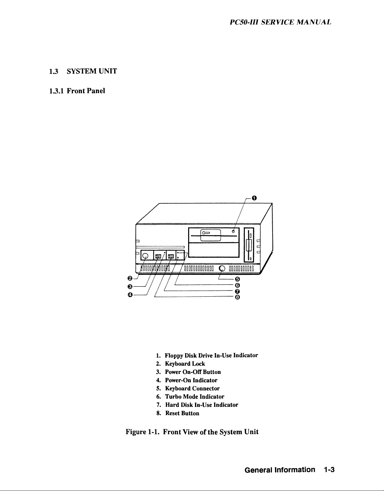
13.1 Front Panel
1. Floppy Disk Drive In-Use Indicator
2. Keyboard Lock
3. Power On-Off Button
4. Power-On Indicator
5. Keyboard Connector
6. Turbo Mode Indicator
7. Hard Disk In-Use Indicator
8. Reset Button
Figure 1-1. Front View of the System Unit
General Information
1-3
Page 18
PC50-III SERVICE MANUAL
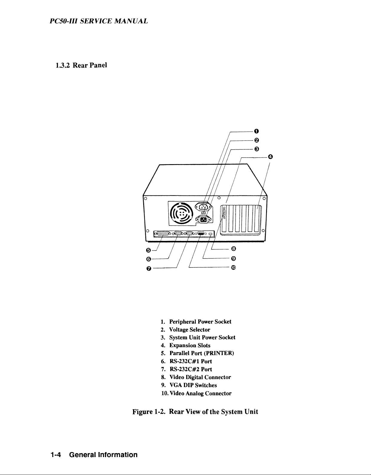
13.2 Rear Panel
1. Peripheral Power Socket
2. Voltage Selector
3. System Unit Power Socket
4. Expansion Slots
5. Parallel Port (PRINTER)
6. RS-232C#1 Port
7. RS-232C#2 Port
8. Video Digital Connector
9. VGA DIP Switches
10. Video Analog Connector
Figure 1-2. Rear View of the System Unit
1-4 General Information
Page 19
PC50-III SERVICE MANUAL
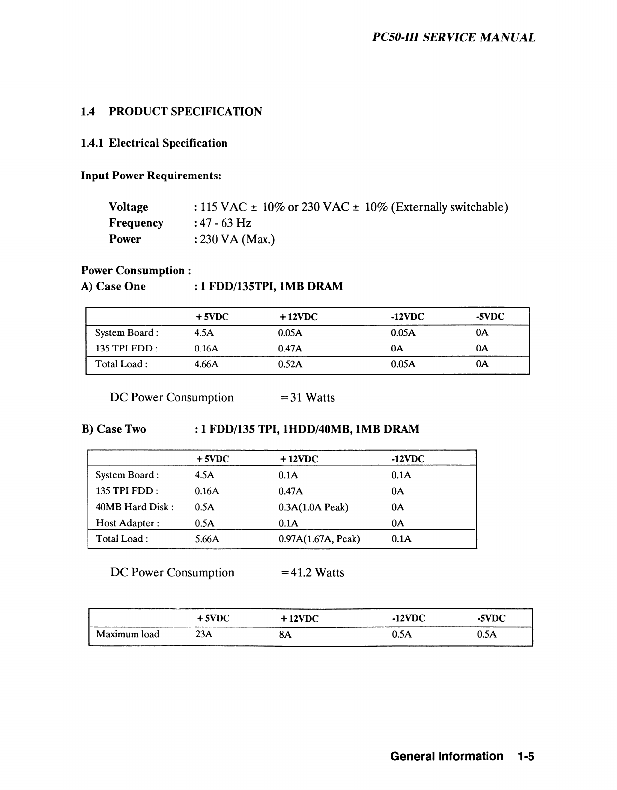
1.4 PRODUCT SPECIFICATION
1.4.1 Electrical Specification
Input Power Requirements:
Voltage : 115 VAC ± 10% or 230 VAC ± 10% (Externally switchable)
Frequency : 47 - 63 Hz
Power : 230 VA (Max.)
Power Consumption:
A) Case One : 1 FDD/135TPI, 1MB DRAM
+ 5VDC
+ 12VDC
-12VDC
-5VDC
System B oa rd : 4.5A
0.05A
0.05A
0A
135 TPI FDD :
0.16A 0.47A 0A
0A
Total L oa d :
4.66A
0.52A
0.05A 0A
DC Power Consumption
= 31 Watts
B) Case Two : 1 FDD/135 TPI, 1HDD/40MB, 1MB DRAM
+ 5VDC + 12VDC -12VDC
System B oa rd : 4.5A
0.1 A 0.1A
135 TPI FDD :
0.16 A
0.47A 0A
40MB H ard D isk :
0.5A
0.3A(1.0A Peak)
0A
Host A dapter:
0.5A 0.1A
0A
Total L oa d :
5.66A
0.97A(1.67A, Peak)
0.1A
DC Power Consumption
= 41.2 Watts
+ 5VDC
+ 12VDC
-12VDC
-5VDC
Maximum load
23A
8A
0.5A 0.5A
General Information 1-5
Page 20
PC50-III SERVICE MANUAL
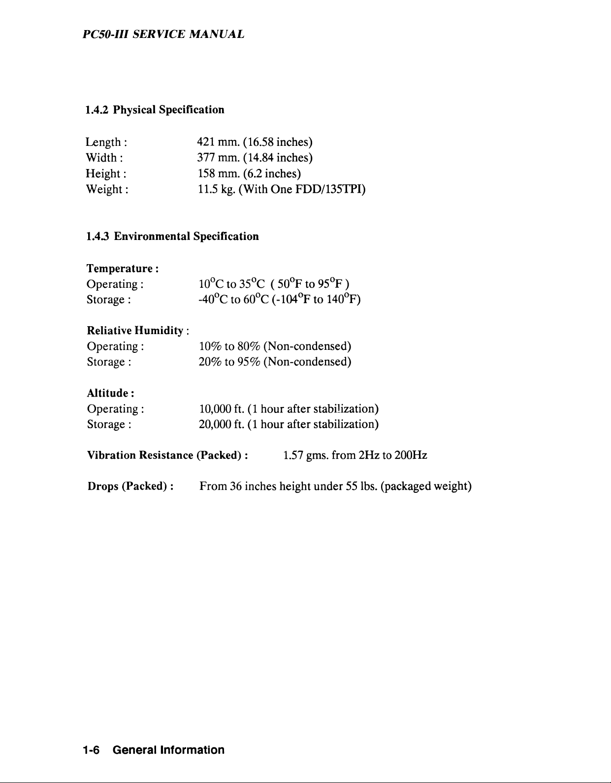
1.4.2 Physical Specification
Length:
Width:
Height:
Weight:
421 mm. (16.58 inches)
377 mm. (14.84 inches)
158 mm. (6.2 inches)
11.5 kg. (With One FDD/135TPI)
1.43 Environmental Specification
Temperature:
Operating:
Storage :
10°C to 35°C ( 50°F to 95°F)
-40°C to 60°C (-104°F to 140°F)
Reliative Humidity:
Operating:
Storage:
10% to 80% (Non-condensed)
20% to 95% (Non-condensed)
Altitude:
Operating:
Storage:
10.000 ft. (1 hour after stabilization)
20.000 ft. (1 hour after stabilization)
Vibration Resistance (Packed) : 1.57 gms. from 2Hz to 200Hz
Drops (Packed): From 36 inches height under 55 lbs. (packaged weight)
1-6
General Information
Page 21
PC50-III SERVICE MANUAL
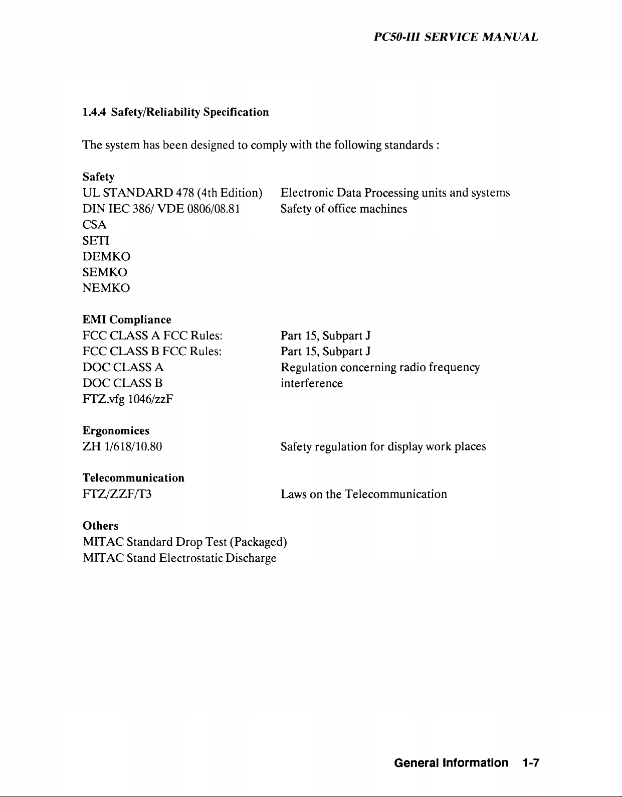
1.4.4 Safety/Reliability Specification
The system has been designed to comply with the following standards :
Safety
UL STANDARD 478 (4th Edition) Electronic Data Processing units and systems
DIN IEC 386/ VDE 0806/08.81 Safety of office machines
CSA
SETI
DEMKO
SEMKO
NEMKO
EMI Compliance
FCC CLASS A FCC Rules: Part 15, Subpart J
FCC CLASS B FCC Rules: Part 15, Subpart J
DOC CLASS A Regulation concerning radio frequency
DOC CLASS B interference
FTZ.vfg 1046/zzF
Ergonomices
ZH 1/618/10.80 Safety regulation for display work places
Telecommunication
FTZ/ZZF/T3 Laws on the Telecommunication
Others
MIT AC Standard Drop Test (Packaged)
MIT AC Stand Electrostatic Discharge
General Information
1-7
Page 22
PC50-III SERVICE MANUAL
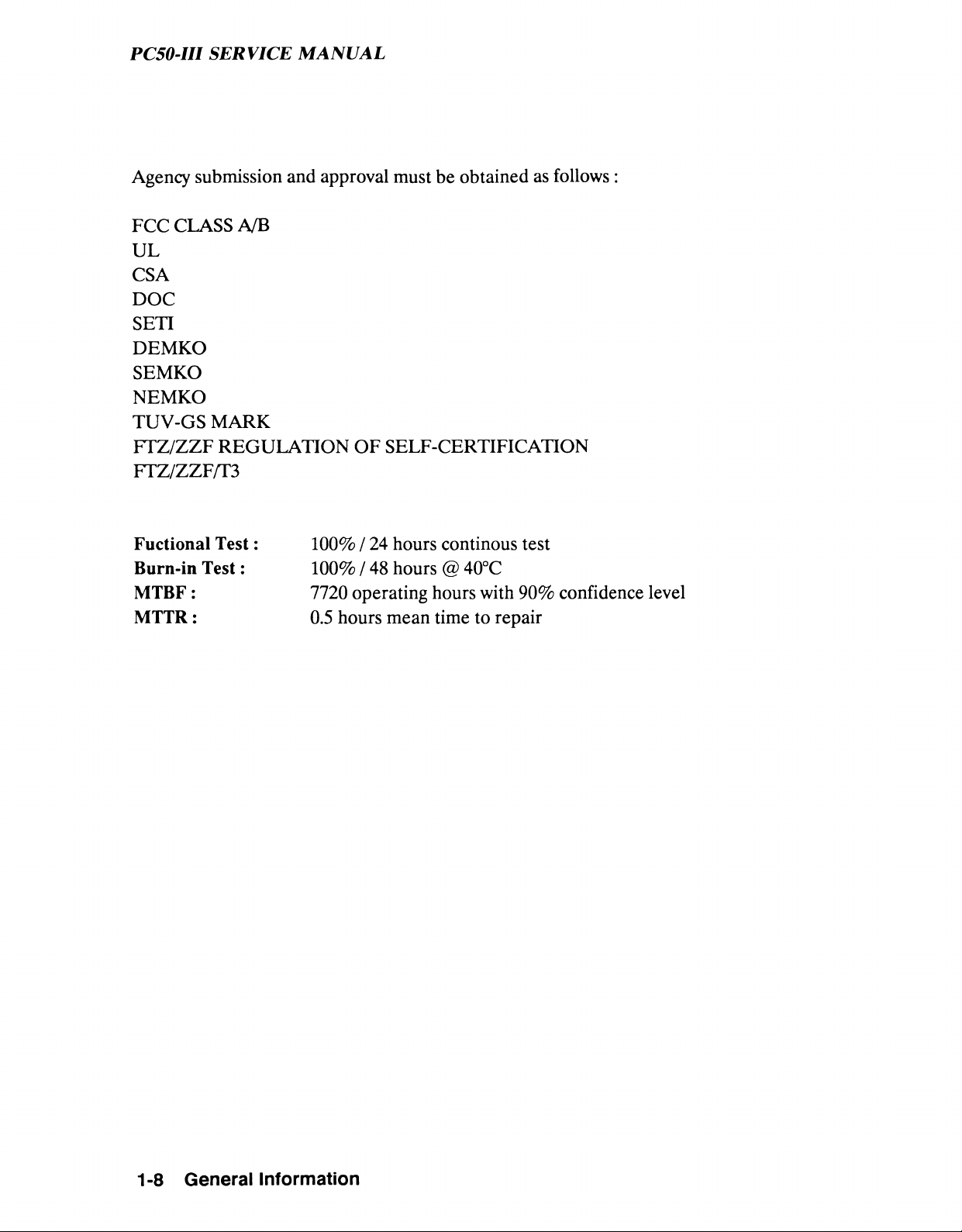
Agency submission and approval must be obtained as follows :
FCC CLASS A/B
UL
CSA
DOC
SETI
DEMKO
SEMKO
NEMKO
TUV-GS MARK
FTZ/ZZF REGULATION OF SELF-CERTIFICATION
FTZ/ZZF/T3
Fuctional Test:
Burn-in Test:
MTBF:
MTTR:
100% / 24 hours continous test
100%/48 hours @40°C
7720 operating hours with 90% confidence level
0.5 hours mean time to repair
1-8 General Information
Page 23
PC50-III SERVICE MANUAL
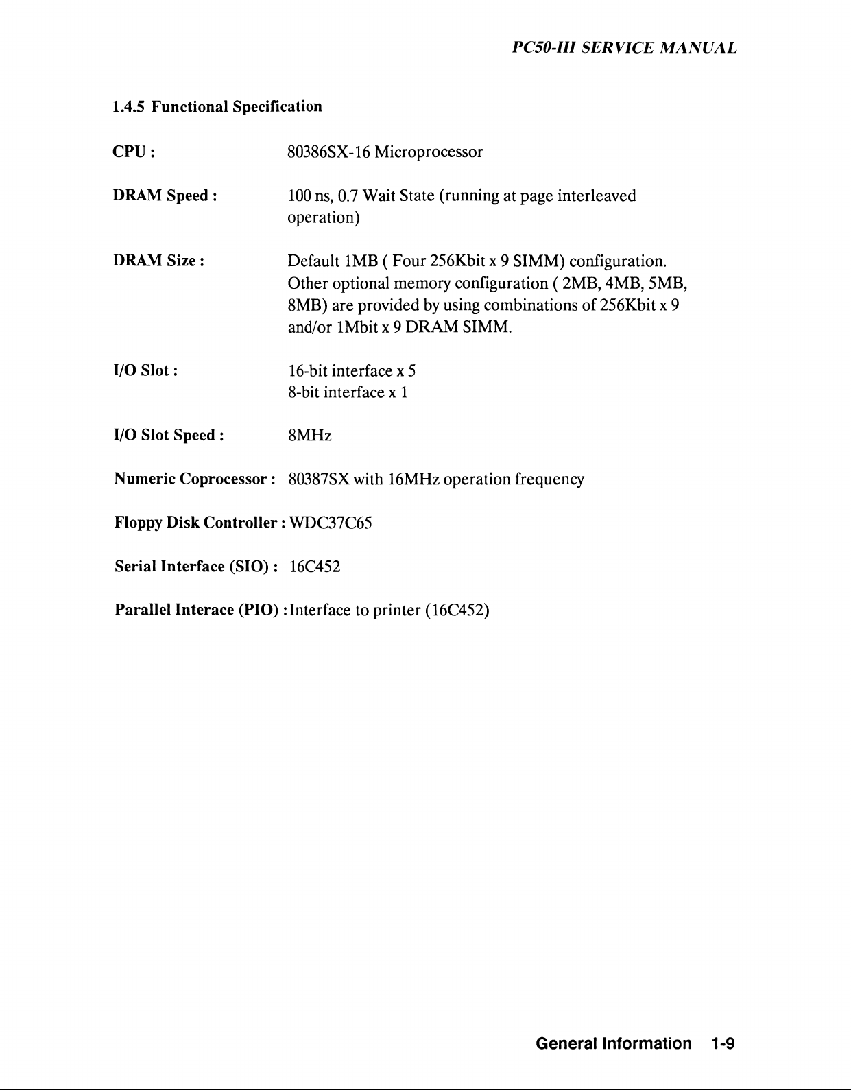
1.4.5 Functional Specification
CPU: 80386SX-16 Microprocessor
DRAM Speed:
100 ns, 0.7 Wait State (running at page interleaved
operation)
DRAM Size:
Default 1MB ( Four 256Kbit x 9 SIMM) configuration.
Other optional memory configuration ( 2MB, 4MB, 5MB,
8MB) are provided by using combinations of 256Kbit x 9
and/or 1Mbit x 9 DRAM SIMM.
I/O Slot:
16-bit interface x 5
8-bit interface x 1
I/O Slot Speed:
8MHz
Numeric Coprocessor:
80387SX with 16MHz operation frequency
Floppy Disk Controller: WDC37C65
Serial Interface (SIO): 16C452
Parallel Interace (PIO ): Interface to printer (16C452)
General Information 1-9
Page 24

Page 25
PC50-III SERVICE MANUAL
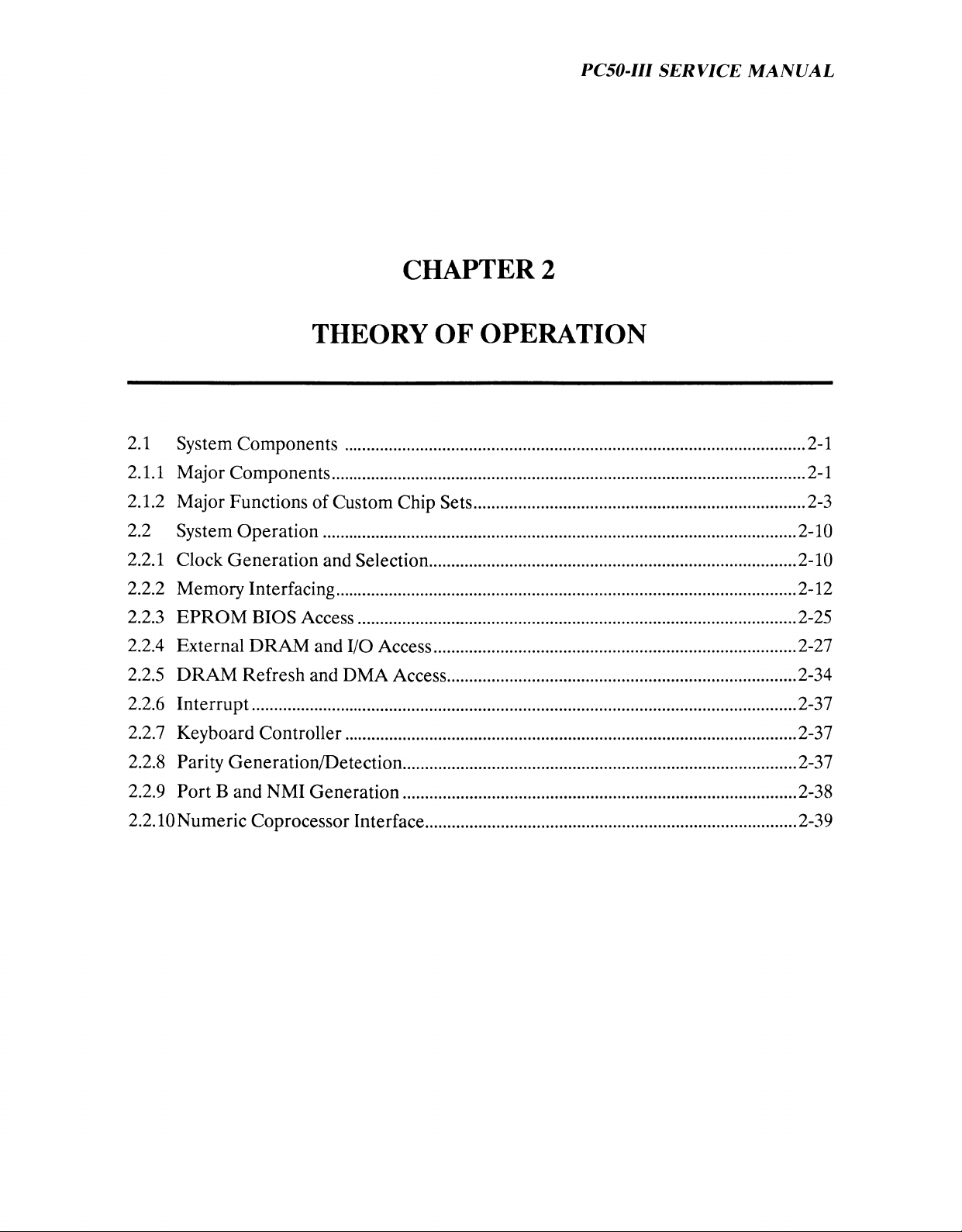
CHAPTER 2
THEORY OF OPERATION
2.1 System Components...................................................................................................2-1
2.1.1 Major Components......................................................................................................2-1
2.1.2 Major Functions of Custom Chip Sets....................................................................... 2-3
2.2 System Operation......................................................................................................2-10
2.2.1 Clock Generation and Selection...............................................................................2-10
2.2.2 Memory Interfacing...................................................................................................2-12
2.2.3 EPROM BIOS Access.............................................................................................. 2-25
2.2.4 External DRAM and I/O Access..............................................................................2-27
2.2.5 DRAM Refresh and DMA Access...........................................................................2-34
2.2.6 Interrupt.....................................................................................................................2-37
2.2.7 Keyboard Controller.................................................................................................2-37
2.2.8 Parity Generation/Detection.....................................................................................2-37
2.2.9 Port B and NMI Generation.....................................................................................2-38
2.2.10 Numeric Coprocessor Interface................................................................................2-39
Page 26

Page 27
PC50-III SERVICE MANUAL
2.1 SYSTEM COMPONENTS
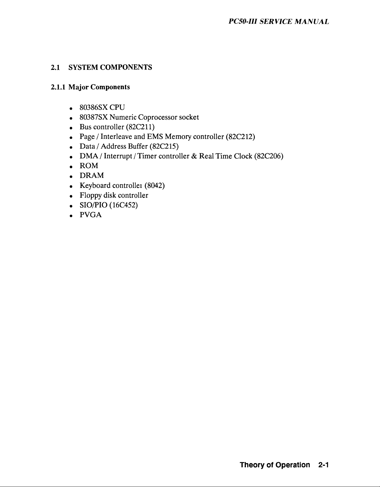
2.1.1 Major Components
• 80386SX CPU
• 80387SX Numeric Coprocessor socket
• Bus controller (82C211)
• Page / Interleave and EMS Memory controller (82C212)
• Data / Address Buffer (82C215)
• DMA / Interrupt / Timer controller & Real Time Clock (82C206)
• ROM
• DRAM
• Keyboard controller (8042)
• Floppy disk controller
. SIO/PIO (16C452)
• PVGA
Theory of Operation 2-1
Page 28
PC50-III SERVICE MANUAL
LA17-23
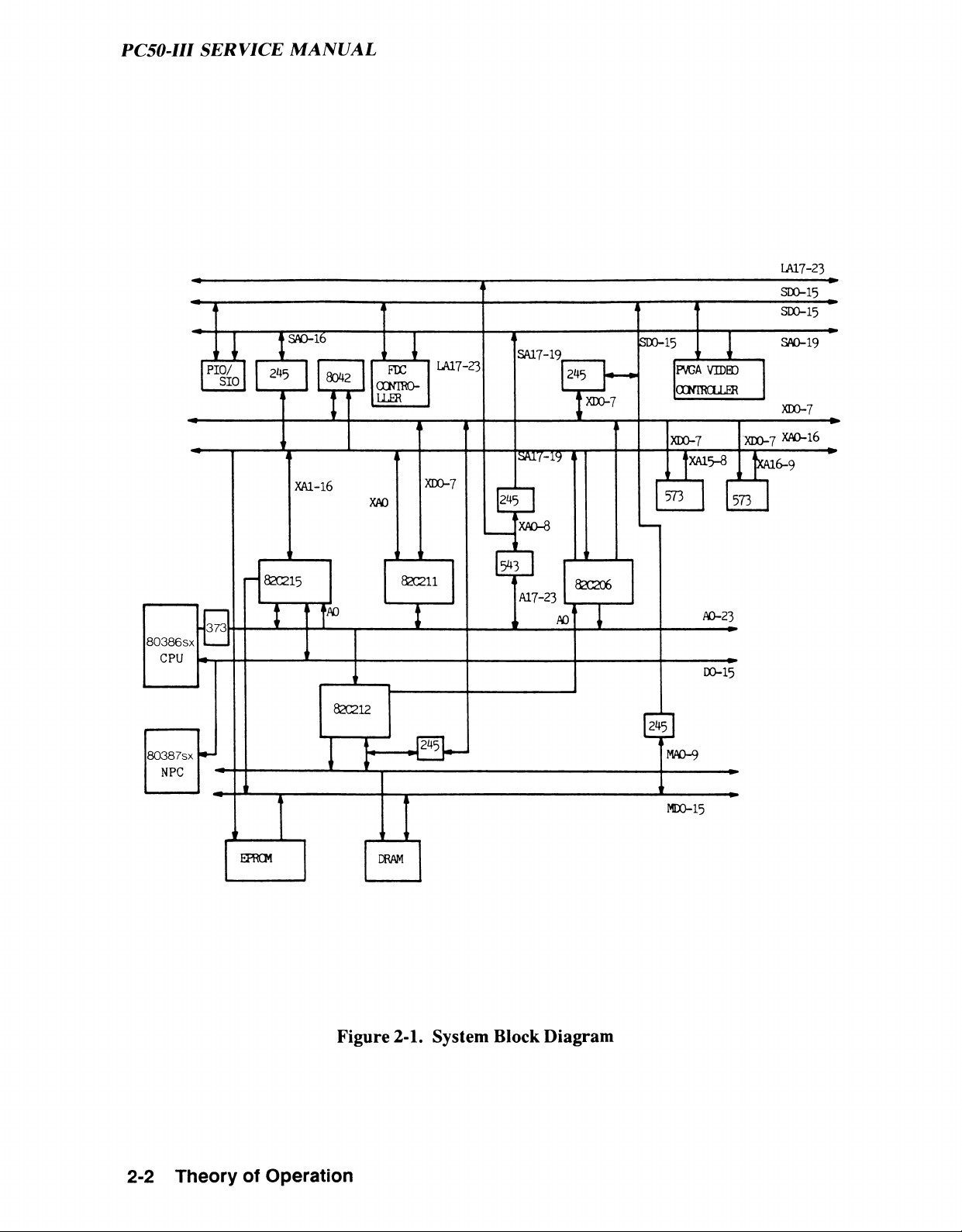
Figure 2-1. System Block Diagram
2-2
Theory of Operation
Page 29
PC50-III SERVICE MANUAL
2.1.2 Major Function of Custom Chip Sets
The system board has the flexiblility to allow you to configure the system by adding selected
peripherals. It serves as a communication center for the Central Processing Unit (CPU),
controllers and peripherals. There are five custom chip sets comprising the major function
of the system board. They are described as follows :
82C211
The 82C211 is the Bus controller which generates control signals, processor clock (PROC-
CLK) and the AT Bus system clock for the entire system. Signals from the 82C211 are used
throughout the system for control and steering of logic. All bus cycles are decoded and
timed by this device. The system status and control port which is referred to as Port B is
also integrated in the 82C211. The 82C211 functions as the one part which holds the entire
system together.
82C215
The 82C215 is the System Data/Address Bus buffer. In the process of providing data bus
buffering, two related functions are provided by the 82C215. Since the 80386SX is a 16-bit
data bus CPU, transfers of 16-bit data to and from 8-bit devices require additional logic.
This additional logic to perform the latching and low/high byte conversion are included in
the 82C215. Another function of the 82C215 is parity generation and checking of the
system. If the parity error is detected, the 82C215 flags a parity error on the PARERR
output line to the 82C211.
Theory of Operation
2-3
Page 30
PC50-III SERVICE MANUAL
82C212
The 82C212 is the Page/Interleaved and EMS Memory controller. It performs memory
control functions utilizing page/interleaved mode of operation to access DRAMs. The
82C212 supports the Lotus/Intel/Microsoft (LIM) Expanded Memory System (EMS) ad
dress translation logic. It maps a 64KB block of memory at C0000H to EFFFFH of the
EPROM to anywhere between the 1MB to 8MB RAM space. For efficient execution of
BIOS, it is preferable to execute BIOS code through RAM rather than through slower
EPROMs. The 82C212 provides the Shadow RAM feature which allows the BIOS code to
be executed from system RAM, resident at the same physical address as the BIOS EPROM.
Also integrated in the 82C212 are the DRAM refresh logic and 14.31818 MHz, 1.1938MHz
clock generation logic.
82C206
The 82C206 Integrated Peripheral controller incorporates two 8237 DMA controllers, two
8259 Interrupt controllers, one 8254 Timer/Counter, one MC146818 real-time clock, a
74LS612 memory mapper, and several other TTL/SSI interface logic chips. This offer a
single chip integration of all the peripherals attached to the peripheral bus (X-bus). On top
of complete compatibility to the AT architecture, the chip offers enhanced features and
improved speed performance. These include an additional 64 bytes of RAM for the Real
Time Clock and reduced recovery specifications for the 8237, 8259, and 8254. A variable
wait state option is provided for the DMA cycles. Programmable delays are provided for
the CPU to access the internal registers of the chip. This chip also includes an option to
select either an 8 or 4 MHz system clock.
PVGA1 Chip
The PVGA1 is a 1.5 micron CMOS custom LSI device, packaged in a 100-pin plastic leadless
chip carrier. It is a single chip video controller that is compatible, in all modes, with the
IBM VGA.
2-4
Theory of Operation
Page 31
PC50-III SERVICE MANUAL
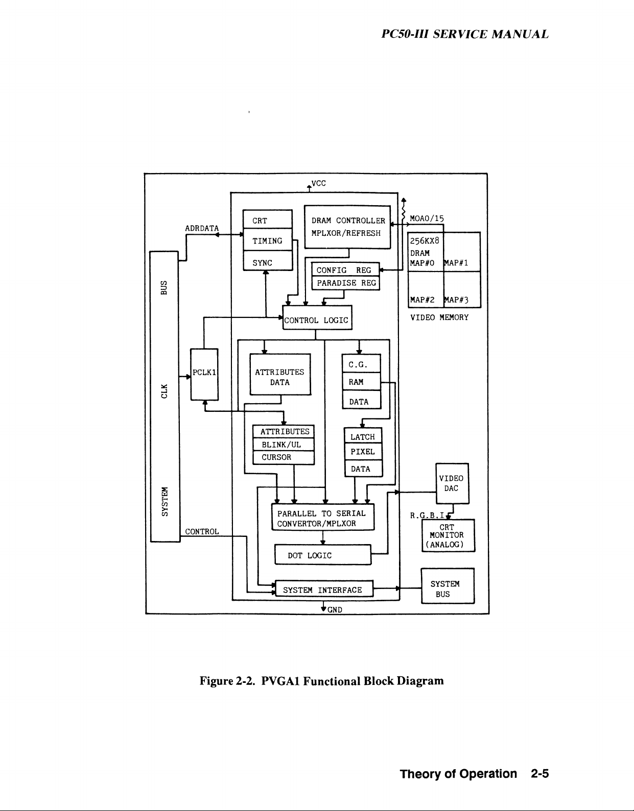
Figure 2-2. PVGA1 Functional Block Diagram
Theory of Operation
2-5
Page 32
PC50-III SERVICE MANUAL
PVGA1 Design Architechture
The PVGA1 system architecture can be separated into four sections:
• Sequencer
• CPU Interface
• Video Controller
• CRT Controller
The PVGA1 block diagram describes the system architecture and the interrelation of the
four main sections. It illustrates how the PVGA1 provides the interface logic between the
display memory and the CRT monitor. The display memory control, memory refresh, and
video drive signals are provided by the PVGA1 chip. The PVGA1 also contains all of the
VGA and special control registers.
The CPU interaface allows the CPU to write to individual planes or to write 32 bit words
to all four planes in one CPU write cycle, all under the control of the Map Select Register.
Sequencer
The Sequencer is responsible for :
• Generating Display Memory RAS and CAS Timing
• Generating the Output Enable Signals for the Display Memory Planes.
• Generating the Character Clock
• Producing the Character Font Select Signals
The Sequencer contains registers for controlling display resolution, selection of character
fonts, and management of the display memory access.
The PVGA1 has a unique design which results in more efficient bandwidth for the display
memory.
2-6 Theory of Operation
Page 33
PC50-III SERVICE MANUAL
The PVGA1 Sequencer gives every memory cycle to the CRT Controller (CRTC) unless
the CPU needs to access the display memory. If the CPU has not accessed the display
memory for four or more memory cycles, then the CPU will be allowed to access display
memory at the end of the next RAS cycle. The next four memory cycles then belong to the
CRT Controller. The first three of these four CRT memory cycles are shortened by two
clock periods to make up for the six clock periods (640 x 350 mode) stolen by the CPU for
memory access. The fourth and successive CRT cycles continue to access the memory as
usual. This technique is known as rubber banding.
CPU Interface
The purpose of the CPU interface is to provide the link between the display hardware and
the system CPU. Integrated in the CPU interface are four 8-bit data latches (one 8-bit latch
per memory plane), which latch display memory data on each CPU read operation. The
outputs of these four 8-bit latches interface to the CPU data bus via a multiplexer.
The particular plane read by the CPU depends on the value stored in bits D0-D3 of the
Read Map Select Register 3CF index 04H. Data written to the display memory by the CPU
may be rotated or logically operated upon, depending on the value stored in bits D0-D4 of
the Data Rotate Register 3CF index 03H. The modified data is written to the display
memory via a multiplexer, which selects the even or odd memory planes controlled by bit
D2 of the Memory Mode Set Register (C5 index 04) in the Sequencer. The planes written
are also dependent on the value stored in bits D0-D3 of the Map Mask Register (3C5 index
02) in the Sequencer.
Theory of Operation 2-7
Page 34
PC50-III SERVICE MANUAL
Video Controller
The PVGA1 Video Controller section includes the graphics and attribute control logic.
Four 8-bit latches (one 8-bit latch per memory plane) are loaded with display data each
time video accesses display memory. Addressing of the display memory is accomplished by
the CRT Control section of the PVGA1. When in Graphics mode, each memory plane can
be selectively mapped one at a time or in any combination. For example, when attribute
mode control register bit 6 equals 0, all memory maps may be enabled where each of the 4
bits (one bit from each plane at the same display memory address) contributes to define a
particular display pixel. These 4 bits are actually an address to one of sixteen 6-bit palette
registers which contains the 6-bit color information supplied to the monitor. Because there
are sixteen 6-bit registers, the PVGA1 is capable of producing sixteen colors from a palette
of sixty-four. Flowever, when attribute mode control register bit 6 equals 1, the internal
palette of the PVGA1 cannot be used to select the external palette in the video DAC. The
video DAC is used to produce 256 colors from a palette of 256K.
In the Unchained modes, the shift registers are loaded with each character clock and shifted
with each dot clock. The shifted-out data from each of the four shift registers is supplied
to the attribute controller. The attribute controller acts upon it before passing the video
information on to the monitor.
In the Alphanumeric mode, the even address data form plane 0 (Character data) is used by
the CRT Controller to address the character generator in character maps 2 or 3. The
character produced by the character maps is loaded into shift register 2 or 3 and shifted out
serially as video data. The odd address data form plane 1 (attribute data) is loaded into the
parallel-in/parallel-out shift register 1, which passes the data on to the attribute controller.
In addition to addressing the upper 8 palette registers, attribute bit can select an alternate
character map defined by Map Select Register 3C5 Index 03.
2-8
Theory of Operation
Page 35
PC50-III SERVICE MANUAL
The Video Controller hardware provides the capability to chain the even memory maps to
the odd. This is accomplished by feeding the shifted-out data form odd shift registers to
the input of the preceding even shift registers. The shift registers are then loaded with
alternate character clocks. Likewise, the display memory is addressed by the CRTC with
alternate even/odd addresses. This capability is particularly useful when simulating a CGA
mode. It is also useful to chain the maps together to provide for more contiguous display
memory when the extended memory is not installed.
The Video Controller section of the PVGA1 contains the Attribute Control Registers.
These registers include the ability to control the color plane selected, horizontal planning,
and border color. The difference between the signals Display Enable and Blank produce
the border area on the display.
CRT Controller
The CRT Controller contains the CRT Control Registers and is responsible for the
horizontal, vertical, and blanking timing for the display monitor. The CRT Controler
induces the cursor generation logic, which provides a signal to the Video Controller
indicating when the cursor is active. The cursor signal is active for the screen character
position determined by the value stored in the cursor position registers. Two additional
registers in the CRT Controller determine the number of scan lines the cursor signal will
be active for this character position.
The CRT Controller section of the PVG A1 is responsible for the video addressing of display
memory. The particular plane accessed by the CRTC depends on the values stored in
several memory access control registers in the other three sections of the PVGA1. Display
memory address signals MA0-MA7 are produced by either the CPU or the CRT Controller.
When produced by the CRTC in Graphics mode, these signals represent latched sequential
addresses to the display memory, directly related to character and scan line count. When
in Alphanumeric mode, MAO-M A7 represents the ASCII character data in the regenerative
buffer (memory plane 0 addressed by the CRTC through MAA0-MAA7) and the row scan
count. In this mode, MAB0-MAB7 is addressing either Character Generator Map 2 or 3
depending on the value of bit 3 of the special Paradise Register. Each 16-bit pair location
in the regenerative buffer represents a character position on the screen and each position
is addressed sequentially by the CRTC on each character clock. The dot matrix size of the
character is dependent on CRTC register programming.
Theory of Operation 2-9
Page 36
PC50-III SERVICE MANUAL
2.2 SYSTEM OPERATION
The detailed operations of the system board are explained as follows :
2.2.1 Clock Generation and Selection
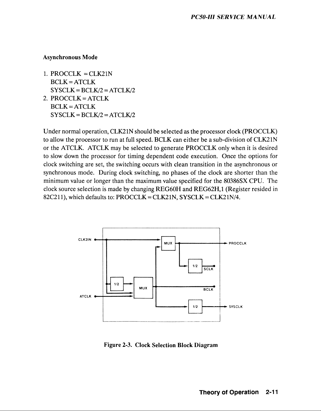
The 82C211 provides a flexible clock selection scheme as shown in Figure 2-3. It has two
input clocks; CLK21N and ATCLK. CLK21N and ATCLK are driven from TTL crystal
oscillators. CLK21N is running at a maximum of twice the processor clock (PROCCLK)
frequency. The ATCLK, typically should be of a lower frequency than CLK21N. ATCLK
and CLK21N can be selected under program control.
The 82C211 generates processor clock PROCCLK for driving the CPU state machine and
interface. SCLK (internal) is PROCCLK/2 and is in phase with the internal states of the
80386SX. BCLK (internal) is the AT bus state machine clock and is used for the AT bus
interface. SYSCLK is the AT bus system clock and is always BCLK/2.
PROCCLK can be derived from CLK21N. In the synchronous mode, both PROCCLK and
BCLK are derived from CLK21N. The asynchronous mode is selected only to generate
BCLK from ATCLK. In this case, PROCCLK is generated from CLK21N or the ATCLK.
BCLK is derived from ATCLK. The folowing clock selections are possible :
Synchronous Mode
1. PROCCLK = BCLK = CLK21N
SYSCLK = BCLK/2 = CLK21N/2
2. PROCCLK = CLK21N
BCLK = CLK21N/2
SYSCLK = BCLK/2 = CLK21N/4
3. PROCCLK = BCLK = CLK21N/2
SYSCLK = BCLK/2 = CLK21N/4
2-10 Theory of Operation
Page 37
PC50-IU SERVICE MANUAL
Asynchronous Mode
1. PROCCLK = CLK21N
BCLK = ATCLK
SYSCLK = BCLK/2 = ATCLK/2
2. PROCCLK = ATCLK
BCLK = ATCLK
SYSCLK = BCLK/2 = ATCLK/2
Under normal operation, CLK21N should be selected as the processor clock (PROCCLK)
to allow the processor to run at full speed. BCLK can either be a sub-division of CLK21N
or the ATCLK. ATCLK may be selected to generate PROCCLK only when it is desired
to slow down the processor for timing dependent code execution. Once the options for
clock switching are set, the switching occurs with clean transition in the asynchronous or
synchronous mode. During clock switching, no phases of the clock are shorter than the
minimum value or longer than the maximum value specified for the 80386SX CPU. The
clock source selection is made by changing REG60H and REG62H,1 (Register resided in
82C211), which defaults to: PROCCLK = CLK2IN, SYSCLK = CLK21N/4.
CLK2IN
ATCLK
PROCCLK
SYSCLK
Figure 2-3. Clock Selection Block Diagram
Theory of Operation 2-11
Page 38
PC50-III SERVICE MANUAL
The 82C212 has an oscillator circuit which uses a 14.31818 MHz crystal to generate the OSC
and OSC/12 clocks. The 1.19381 MHz OSC/12 clock is used internally to generate the RAS
timeout clocks, one for each bank. RAS is deasserted for each bank when its RAS time out
counter times out after about 10 microseconds.
The oscillator circuit in the 82C212 is a very high gain amplifier. Because of this, care should
be taken to prevent the crystal from over driving. Preventing this excessive drive condition
can easily be accomplished by adding a resistor in series with the crystal. This will greatly
improve the long term reliability of the circuit. A resistor with a value of 10 ohms is
sufficient.
2.2.2 Memory Interfacing
Memory Configuration
The 82C212 organizes memory as banks of 18 bit modules, consisting of 16 bits of data and
2 bits of parity information. The 16 bits of data are split into high and low order bytes, with
one parity bit for each byte. This configuration can be implemented by using eighteen 1-bit
wide DRAMs or by using four 4-bit wide DRAMs for data with two 1-bit wide DRAMs for
parity. The minimum configuration can be a single bank operating in non-interleaved
mode or can be a pair of DRAM banks operating in two way interleaved mode. In the
interleaved mode of operation, the DRAMs within a pair of banks must be identical.
However, each bank of DRAM pairs can be different from other pairs. A typical system
may be shipped with one or two banks of smaller DRAM types (256Kbit x 1 DRAMs), and
later upgraded with additional pairs of banks of larger DRAMs (1Mbit x 1 DRAMs).
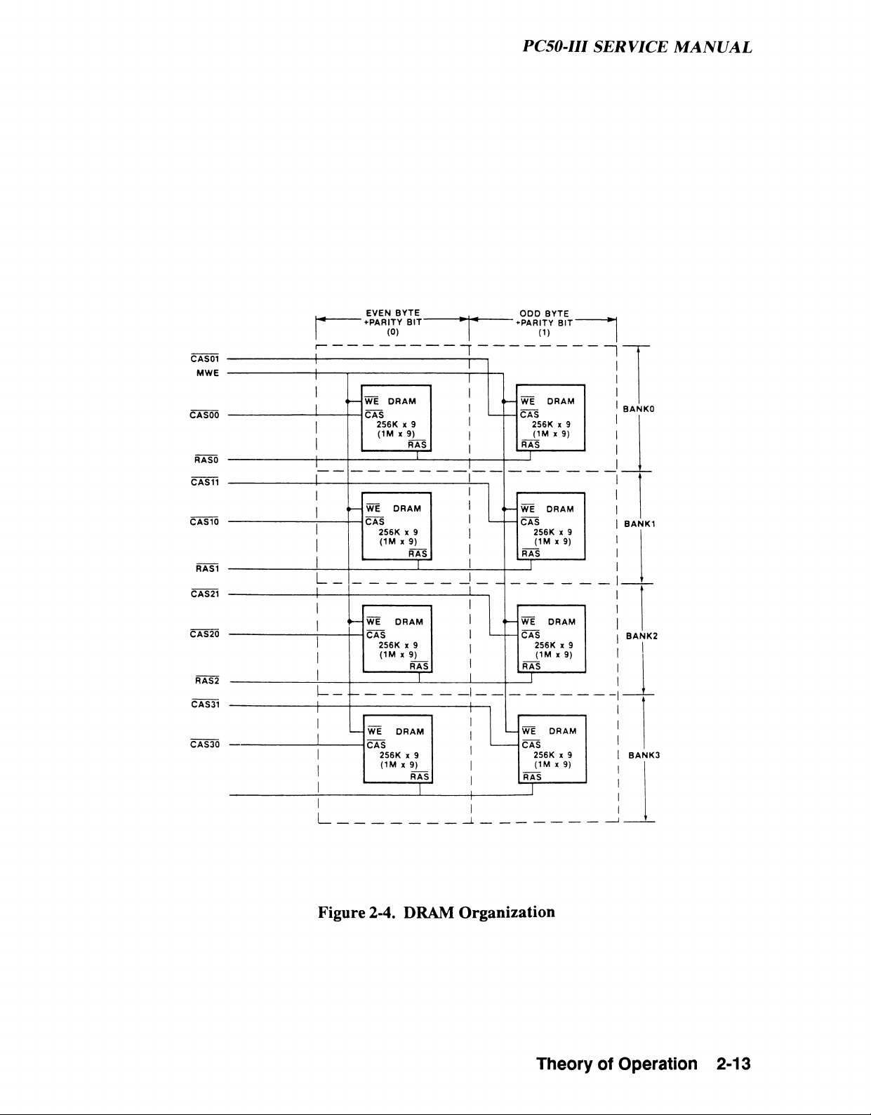
Figure 2-4 is a block diagram of the DRAM organization for the system. As shown, each
RAS line drives a 256Kbit x 18 bank or a 1Mbit x 18 bank. The CAS lines are used to drive
individual bytes within each bank. MWE is connected to each DRAM bank write enable
input.
2-12 Theory of Operation
Page 39
PC50-III SERVICE MANUAL
CAS01
MWE
CASOO
RASO
CAS11
CASIO
RAS1
CAS21
CAS20
RAS2
CAS31
CAS30
EVEN BYTE
♦ PARITY BIT
(0)
ODD BYTE
♦PARITY BIT
( 1)
WE DRAM
CAS
256K x 9
(1M x 9)
__
RAS
WE DRAM
CAS
256K x 9
(1M x 9)
RAS
i
I
WE DRAM
CAS
256K x 9
I
I
i
(1M x 9)
RAS
WE DRAM
CAS
256K x 9
(1M x 9)
RAS
_______
L
I
I
WE DRAM
I
WE DRAM
CAS
I
CAS
256K x 9
I
256K x 9
(1M x 9)
l
(1M x 9)
RAS
I
RAS
U
WE DRAM
CAS
256K x 9
(1M x 9)
__
RAS
WE DRAM
CAS
256K x 9
(1M x 9)
RAS
_______
BANKO
BANK1
BANK2
BANK3
l_
Figure 2-4. DRAM O rganization
Theory of Operation 2-13
Page 40
PC50-IU SERVICE MANUAL
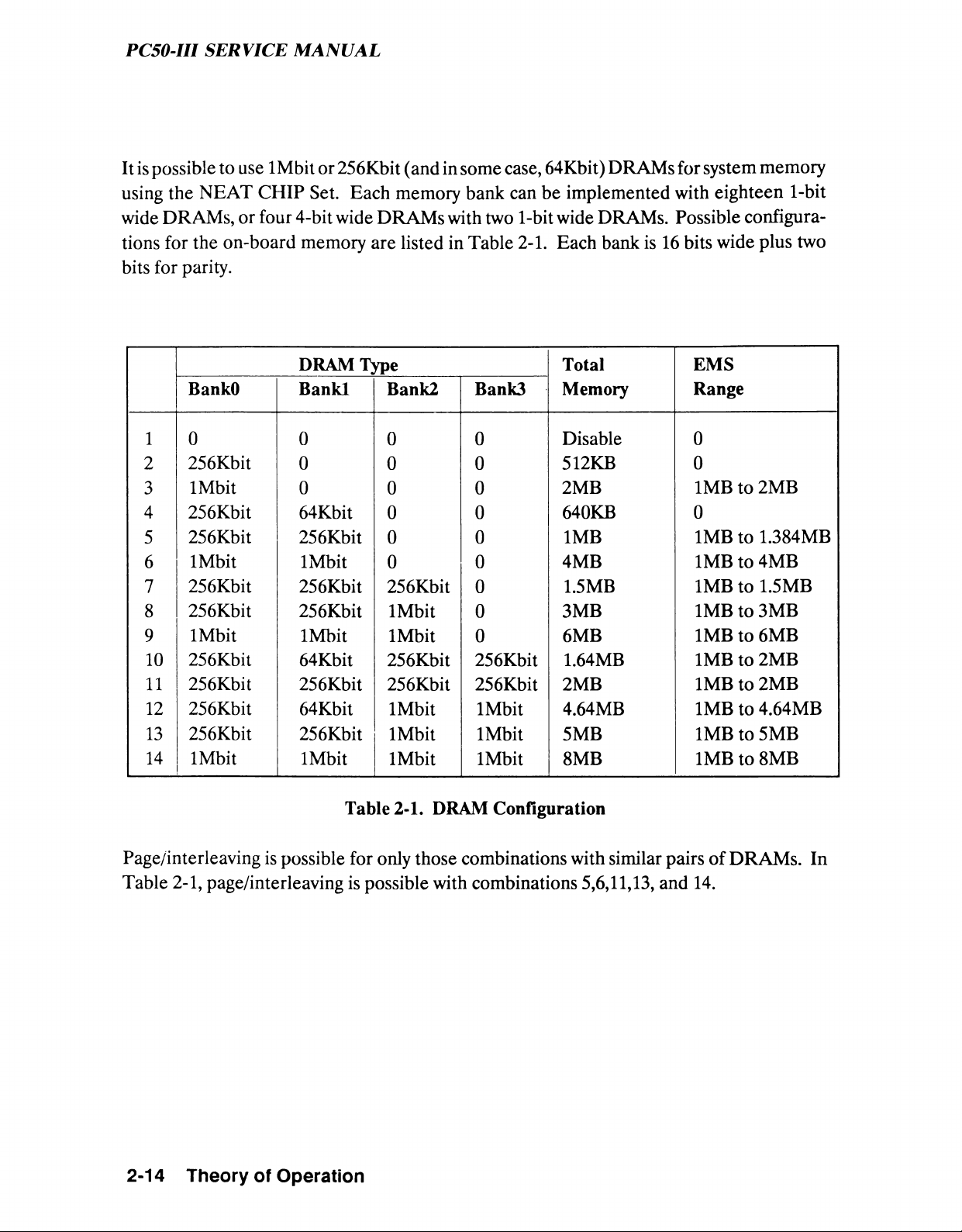
It is possible to use 1Mbit or 256Kbit (and in some case, 64Kbit) DRAMs for system memory
using the NEAT CHIP Set. Each memory bank can be implemented with eighteen 1-bit
wide DRAMs, or four 4-bit wide DRAMs with two 1-bit wide DRAMs. Possible configura
tions for the on-board memory are listed in Table 2-1. Each bank is 16 bits wide plus two
bits for parity.
DRAM T Total
Memory
EMS
Range
BankO
Bankl
Bank2
Bank3
1
0 0 0 0 Disable
0
2 256Kbit
0 0 0
512KB 0
3
1Mbit
0 0 0
2MB
1MB to 2MB
4 256Kbit
64Kbit 0 0
640KB 0
5
256Kbit
256Kbit 0 0
1MB
1MB to 1.384MB
6
1Mbit
1Mbit 0 0
4MB
1MB to 4MB
7
256Kbit
256Kbit 256Kbit 0
1.5MB
1MB to 1.5MB
8 256Kbit
256Kbit 1Mbit 0
3MB
1MB to 3MB
9 1Mbit 1Mbit
1Mbit 0
6MB
1MB to 6MB
10 256Kbit
64Kbit 256Kbit
256Kbit
1.64MB 1MB to 2MB
11
256Kbit
256Kbit 256Kbit 256Kbit
2MB
1MB to 2MB
12
256Kbit
64Kbit 1Mbit 1Mbit
4.64MB 1MB to 4.64MB
13
256Kbit
256Kbit 1Mbit 1Mbit
5MB 1MB to 5MB
14
1Mbit
1Mbit 1Mbit 1Mbit
8MB
1MB to 8MB
Table 2-1. DRAM Configuration
Page/interleaving is possible for only those combinations with similar pairs of DRAMs. In
Table 2-1, page/interleaving is possible with combinations 5,6,11,13, and 14.
2-14 Theory of Operation
Page 41
PC50-UI SERVICE MANUAL
Page/Interleaved Operation
The 82C212 uses a page/interleaved design that is different from most interleaved memory
designs. Typical two way interleaving schemes use two banks of DRAMs, with even word
address on one bank and odd word address on the other bank. If memory accesses are
sequential, the RAS precharge time of one bank overlaps the access time of the other bank.
Typically, programs consist of instruction fetches interspread with operand accesses. The
instruction fetches tend to be sequential and the operand accesses tend to be random.
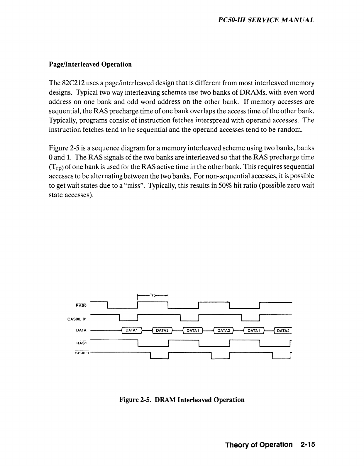
Figure 2-5 is a sequence diagram for a memory interleaved scheme using two banks, banks
0 and 1. The RAS signals of the two banks are interleaved so that the RAS precharge time
(Trp) of one bank is used for the RAS active time in the other bank. This requires sequential
accesses to be alternating between the two banks. For non-sequential accesses, it is possible
to get wait states due to a “miss”. Typically, this results in 50% hit ratio (possible zero wait
state accesses).
RASO
CAS00, 01
DATA
RAS1
-T rp -
T
____
I I
____I---------------
l_ _ l
-----------
— ( DATA1 D — C DATA2
> - c
DATA1 D — C DATA2 ) — ( DATA1 )— ( DATA2
I
Figure 2-5. DRAM Interleaved Operation
Theory of Operation 2-15
Page 42
PC50-III SERVICE MANUAL
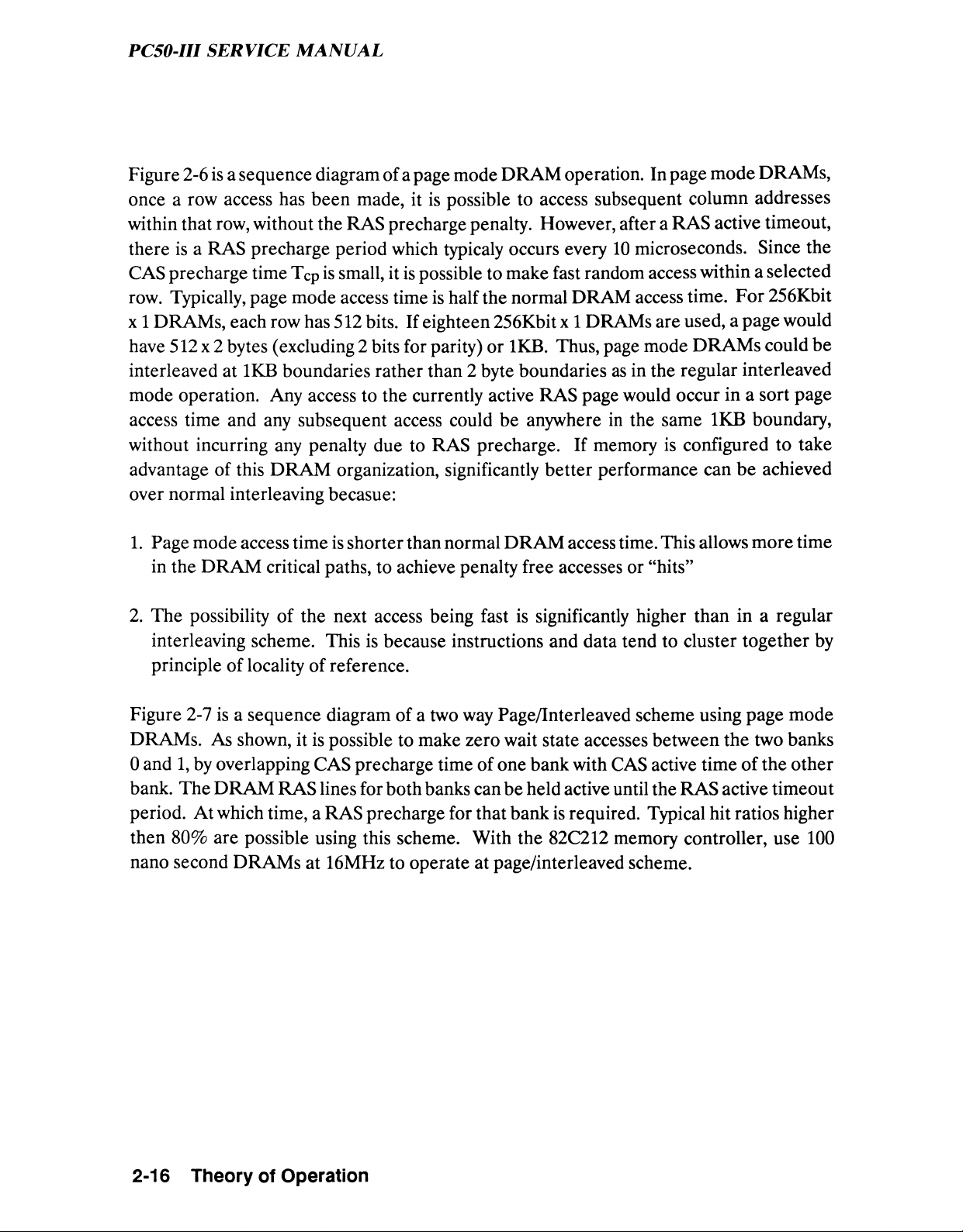
Figure 2-6 is a sequence diagram of a page mode DRAM operation. In page mode DRAMs,
once a row access has been made, it is possible to access subsequent column addresses
within that row, without the RAS precharge penalty. However, after a RAS active timeout,
there is a RAS precharge period which typicaly occurs every 10 microseconds. Since the
CAS precharge time TCp is small, it is possible to make fast random access within a selected
row. Typically, page mode access time is half the normal DRAM access time. For 256Kbit
x 1 DRAMs, each row has 512 bits. If eighteen 256Kbit x 1 DRAMs are used, a page would
have 512 x 2 bytes (excluding 2 bits for parity) or 1KB. Thus, page mode DRAMs could be
interleaved at 1KB boundaries rather than 2 byte boundaries as in the regular interleaved
mode operation. Any access to the currently active RAS page would occur in a sort page
access time and any subsequent access could be anywhere in the same 1KB boundary,
without incurring any penalty due to RAS precharge. If memory is configured to take
advantage of this DRAM organization, significantly better performance can be achieved
over normal interleaving becasue:
1. Page mode access time is shorter than normal DRAM access time. This allows more time
in the DRAM critical paths, to achieve penalty free accesses or “hits”
2. The possibility of the next access being fast is significantly higher than in a regular
interleaving scheme. This is because instructions and data tend to cluster together by
principle of locality of reference.
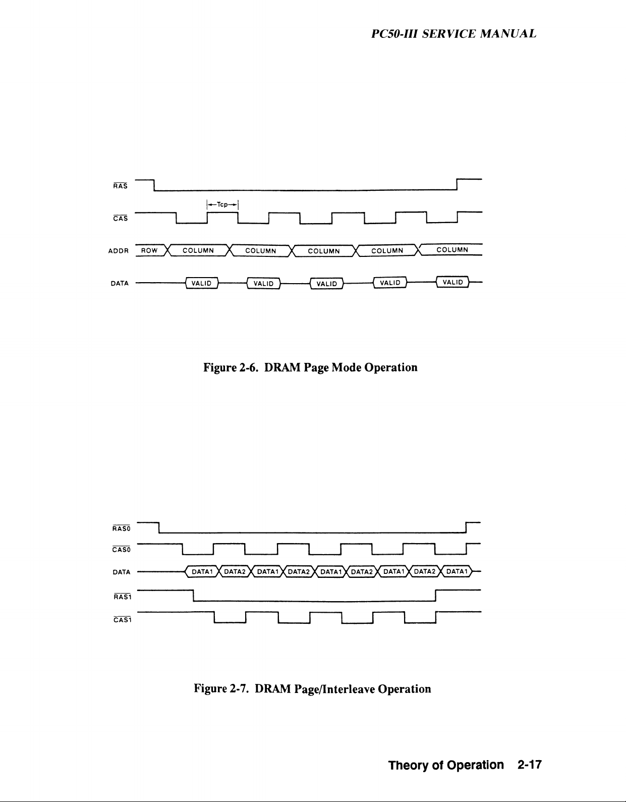
Figure 2-7 is a sequence diagram of a two way Page/Interleaved scheme using page mode
DRAMs. As shown, it is possible to make zero wait state accesses between the two banks
0 and 1, by overlapping CAS precharge time of one bank with CAS active time of the other
bank. The DRAM RAS lines for both banks can be held active until the RAS active timeout
period. At which time, a RAS precharge for that bank is required. Typical hit ratios higher
then 80% are possible using this scheme. With the 82C212 memory controller, use 100
nano second DRAMs at 16MHz to operate at page/interleaved scheme.
2-16
Theory of Operation
Page 43
RAS |_________________________
|— Tcp— I
PC50-III SERVICE MANUAL
i
_
i— i
_ _
r
ADDR ROW )(' CO LUMN
U A I A VA L I U J
Figure 2-6. DRAM Page Mode Operation
RASO
A
COLUMN
i a
-\ VALID /
X
COLU M N )
/ \
( COLUMN
J w aii n V
X
COLU M N
V VAUU r~
CASO
DATA
RAS1
CAS1
- ( DATA1 X DATA2 X DATA1X DATa7)( D ATA1^D A TA 2 X DATA1X DATaT^ DATA1) —
____
i
Figure 2-7. DRAM Page/Interleave Operation
i— i
____
i— i
_____
i— i
____
r
Theory of Operation 2-17
Page 44
PC50-III SERVICE MANUAL
Memory Mapping
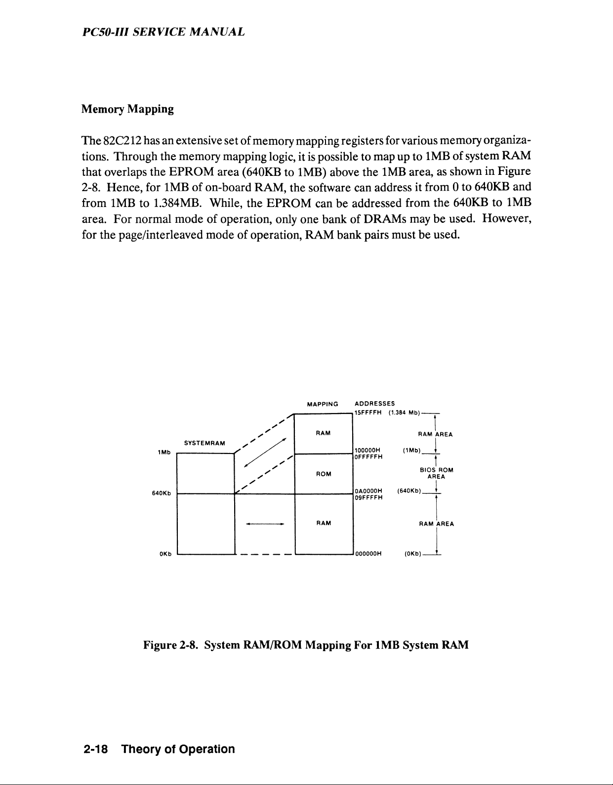
The 82C212 has an extensive set of memory mapping registers for various memory organiza
tions. Through the memory mapping logic, it is possible to map up to 1MB of system RAM
that overlaps the EPROM area (640KB to 1MB) above the 1MB area, as shown in Figure
2-8. Hence, for 1MB of on-board RAM, the software can address it from 0 to 640KB and
from 1MB to 1.384MB. While, the EPROM can be addressed from the 640KB to 1MB
area. For normal mode of operation, only one bank of DRAMs may be used. However,
for the page/interleaved mode of operation, RAM bank pairs must be used.
MAPPING ADDRESSES
RAM AREA
BIOS ROM
AREA
RAM AREA
000000H (0Kb)-
Figure 2-8. System RAM/ROM Mapping For 1MB System RAM
2-18
Theory of Operation
Page 45
PC50-III SERVICE MANUAL
Shadow RAM
For efficient execution of BIOS, it is preferable to execute BIOS code through RAM rather
than through slower EPROMs. The 82C212 provides the shadow RAM feature. If enabled,
it allows the BIOS code to be executed from system RAM, resident at the same physical
address as the BIOS EPROM. Before enabling the shadow RAM feature, the software
should transfer code stored in the BIOS EPROMs to the system RAM. This feature
significantly improves the performance in BlOS-call intensive applications. Performance
improvements as high as 300 to 400% have been observed in benchmark tests on the shadow
RAM. The shadow RAM feature is invoked by enabling the corresponding bits in the ROM
enable register and the RAM mapping register.
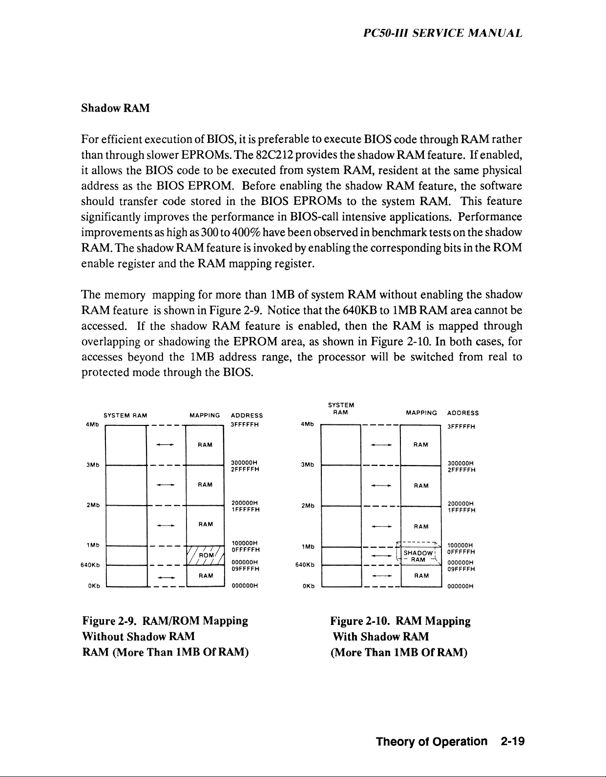
The memory mapping for more than 1MB of system RAM without enabling the shadow
RAM feature is shown in Figure 2-9. Notice that the 640KB to 1MB RAM area cannot be
accessed. If the shadow RAM feature is enabled, then the RAM is mapped through
overlapping or shadowing the EPROM area, as shown in Figure 2-10. In both cases, for
accesses beyond the 1MB address range, the processor will be switched from real to
protected mode through the BIOS.
SYSTEM RAM MAPPING ADDRESS
SYSTEM
RAM MAPPING ADDRESS
3FFFFFH
300000H
2FFFFFH
200000H
1FFFFFH
100000H
0FFFFFH
000000H
09FFFFH
000000H
4Mb
3Mb
2Mb
1Mb
640Kb
0Kb
RAM
RAM
SHADOW'
- RAM
RAM
3FFFFFH
300000H
2FFFFFH
200000H
1FFFFFH
100000H
0FFFFFH
000000H
09FFFFH
Figure 2-9. RAM/ROM Mapping
Without Shadow RAM
RAM (More Than 1MB Of RAM)
Figure 2-10. RAM Mapping
With Shadow RAM
(More Than 1MB Of RAM)
Theory of Operation 2-19
Page 46
PC50-III SERVICE MANUAL
EMS Address Translation Logic
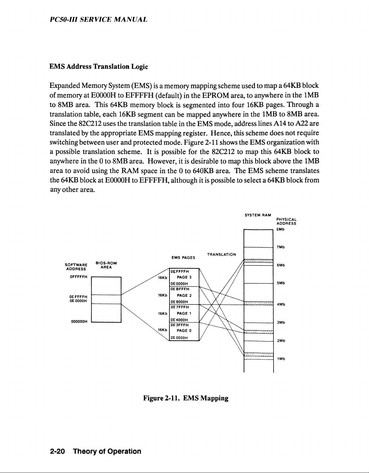
Expanded Memory System (EMS) is a memory mapping scheme used to map a 64KB block
of memory at E0000H to EFFFFH (default) in the EPROM area, to anywhere in the 1MB
to 8MB area. This 64KB memory block is segmented into four 16KB pages. Through a
translation table, each 16KB segment can be mapped anywhere in the 1MB to 8MB area.
Since the 82C212 uses the translation table in the EMS mode, address lines A14 to A22 are
translated by the appropriate EMS mapping register. Hence, this scheme does not require
switching between user and protected mode. Figure 2-11 shows the EMS organization with
a possible translation scheme. It is possible for the 82C212 to map this 64KB block to
anywhere in the 0 to 8MB area. However, it is desirable to map this block above the 1MB
area to avoid using the RAM space in the 0 to 640KB area. The EMS scheme translates
the 64KB block at E0000H to EFFFFH, although it is possible to select a 64KB block from
any other area.
SYSTEM RAM
PHYSICAL
ADDRESS
6Mb
7Mb
6Mb
5Mb
4Mb
3Mb
2Mb
1Mb
2-20
Theory of Operation
Page 47
PC50-III SERVICE MANUAL
The on-board RAM of the MPC2386 system uses 16-bit transfer scheme. All operations
are performed in page mode. If only one bank is used, the operations are non-interleaved.
Interleaved operation mode needs two or four bank memory organization.
On-board DRAM A ccess
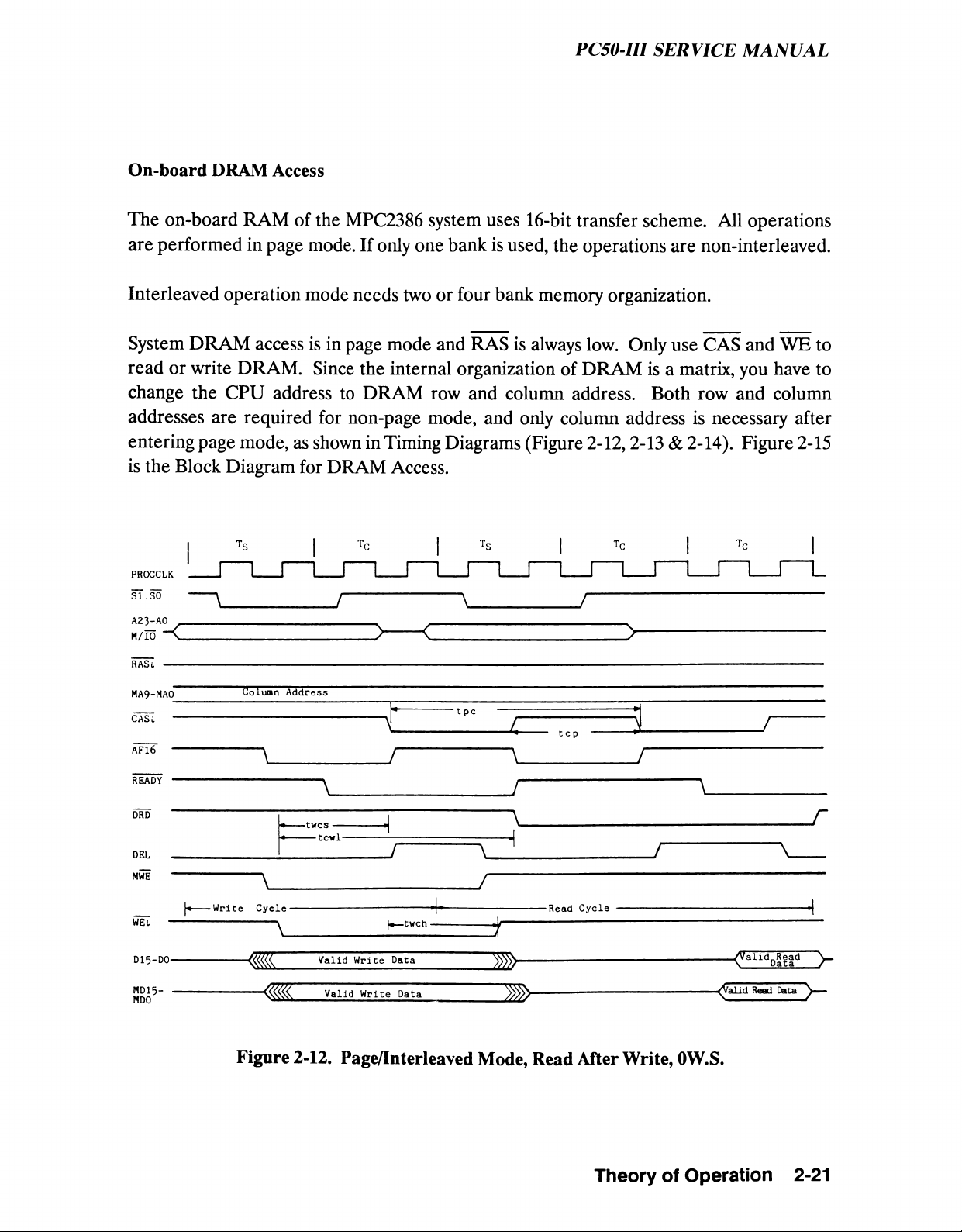
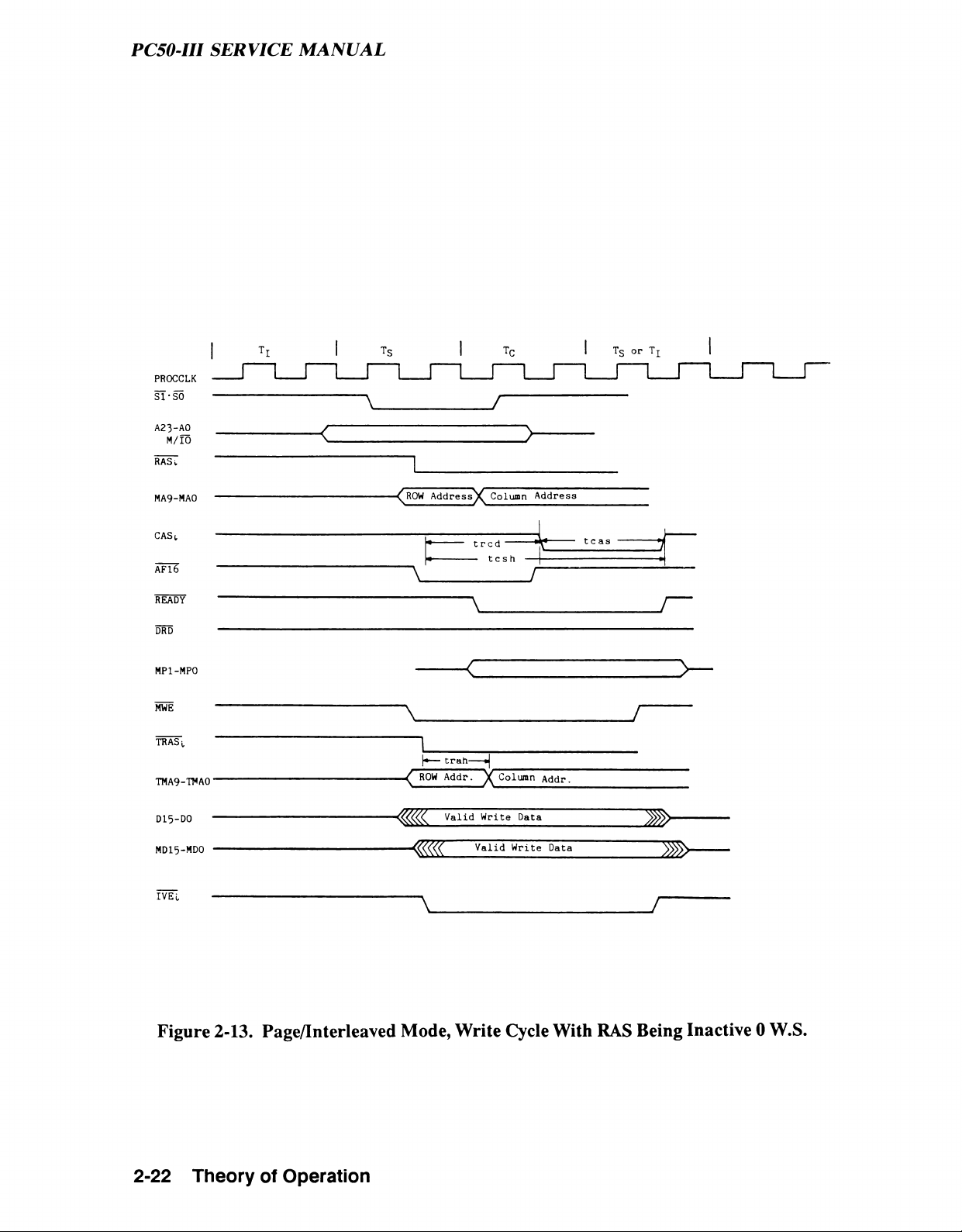
System DRAM access is in page mode and RAS is always low. Only use CAS and WE to
read or write DRAM. Since the internal organization of DRAM is a matrix, you have to
change the CPU address to DRAM row and column address. Both row and column
addresses are required for non-page mode, and only column address is necessary after
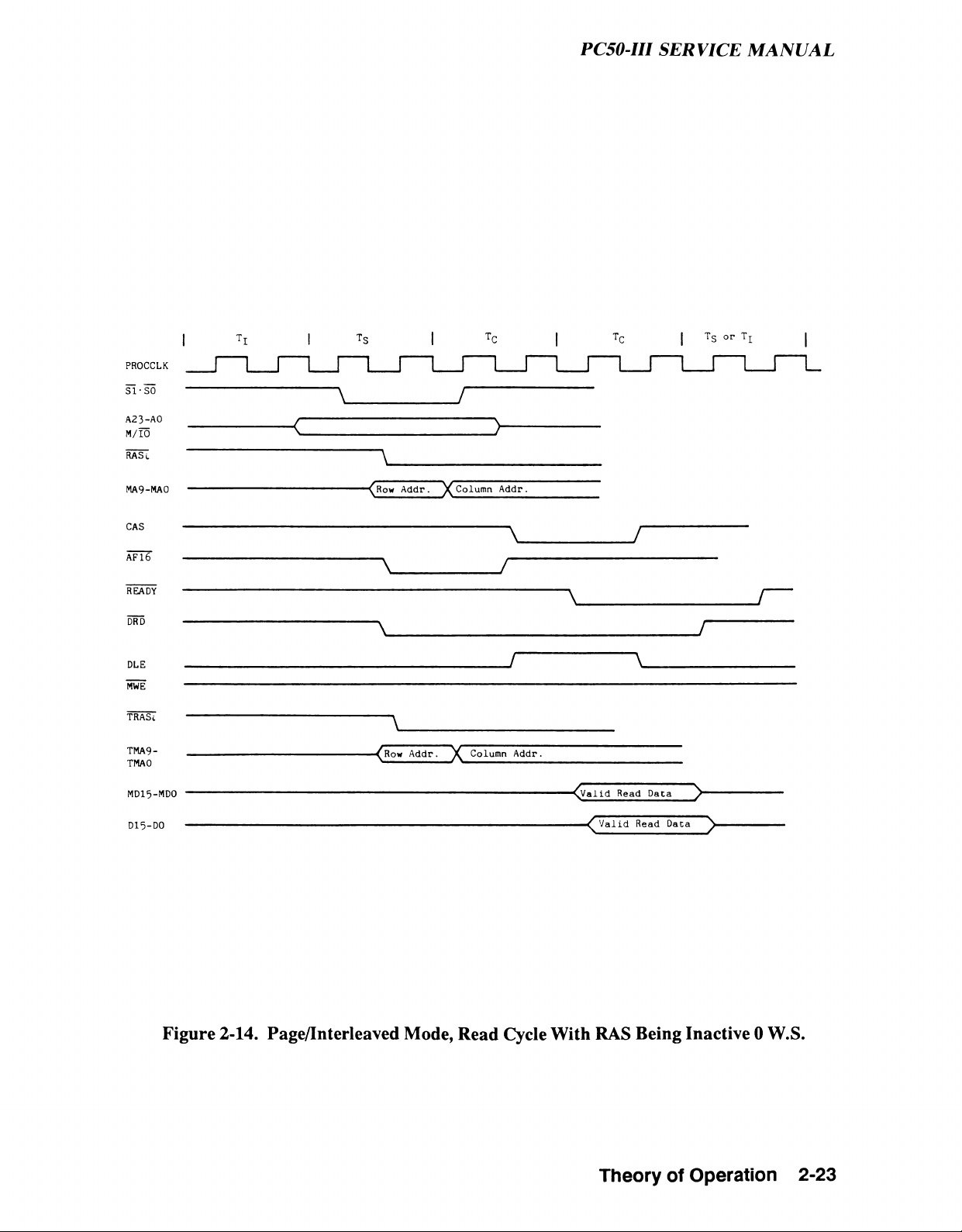
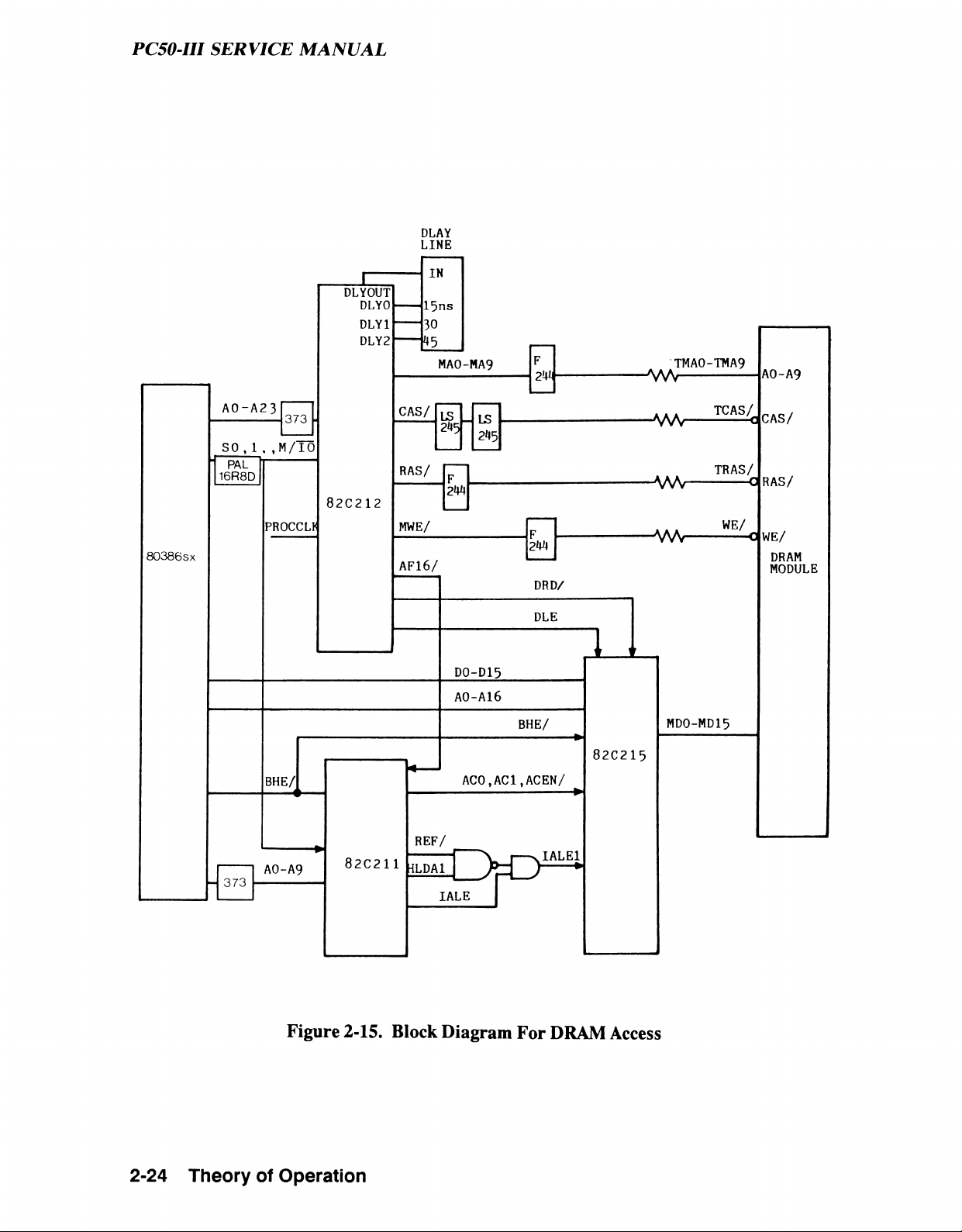
entering page mode, as shown in Timing Diagrams (Figure 2-12,2-13 & 2-14). Figure 2-15
is the Block Diagram for DRAM Access.
PROCCLK
sl.so
A23-AO
M/IO “"C
RASi.
TS
TC
D
------
C
>
Column Address
MA9-MA0
CASc
AF16
READY
DEL
MWE
-tcwl-
-Write Cycle-
WEi
--
1---------------v
" t pc
t c p
-Read Cycle
I*— twch -
■v
D15-D0
MD15-
MDO
Valid Write Data —
Valid Write Data
_ >
^/aild Read Data
> -
Figure 2-12. Page/Interleaved Mode, Read After Write, OW.S.
Theory of Operation 2-21
Page 48
PC50 III SERVICE MANUAL
MA9-MA0
CASt
AF16
READY
DRD
ROW Ad dress^ Column Address
----------------
--------
^
_
________
_
- treu "
\ u v- ao J
r tCjft
^
___________
f
^
_____________________
/
MP1-MP0
MWE
TRAS't
TMA9-TWA0
D15-D0
MD15-MD0
\
_______________________
f
(♦ t r a h —— *|
Y ROW Addr Y Column Addr
' « « Valid Write Data
m —
— Valid Write Data
»»>
IVEL
\
/
Figure 2-13. Page/Interleaved M ode, W rite Cycle W ith RAS Being Inactive 0 W .S.
2-22 Theory of Operation
Page 49
PC50-III SERVICE MANUAL
PROCCLK
SI- SO
A23-A0
m/To
RASi
MA9-MA0
Tr | TS | TC | Tc | TS °r TI
A
____________
f
< >
\
^Row Addr
Column AddrT
CAS
AF16
READY
DRD
DLE
MWE
\
\
TRASc
TMA9-
TMAO
MD15-MDO
D15-DO
“ A
_______________
^Row Addr. Column Addr.
■^Valid Read Data ^
<
Valid Read Daca
>
Figure 2-14. Page/Interleaved Mode, Read Cycle W ith RAS Being Inactive 0 W .S.
Theory of Operation 2-23
Page 50
PC50-III SERVICE MANUAL
DLAY
LINE
Figure 2-15. Block Diagram For DRAM Access
2-24 Theory of Operation
Page 51
PC50-III SERVICE MANUAL
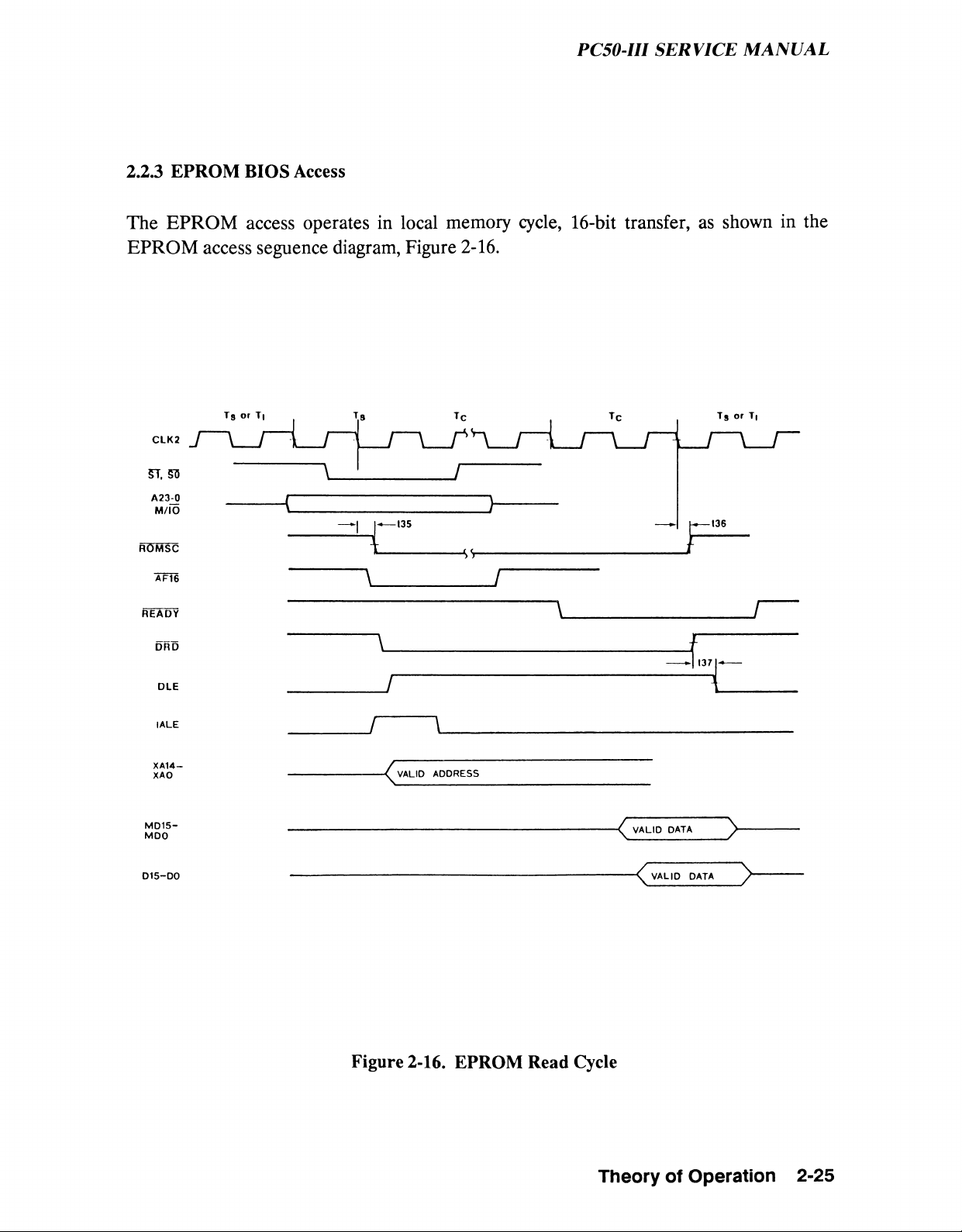
The EPROM access operates in local memory cycle, 16-bit transfer, as shown in the
EPROM access seguence diagram, Figure 2-16.
2.2.3 EPROM BIO S Access
AF16 \
________________
f
READY \ f
DRD
V
t
--
—*
137
i*—
DLE
_____________
/
J
J
l
XA14-
XAO
VALID ADDRESS
MD15-
MDO
■/v A L ID DATA
>
D15-DO
<
VALID DATA
>
Figure 2-16. EPROM Read Cycle
Theory of Operation 2-25
Page 52
PC50-III SERVICE MANUAL
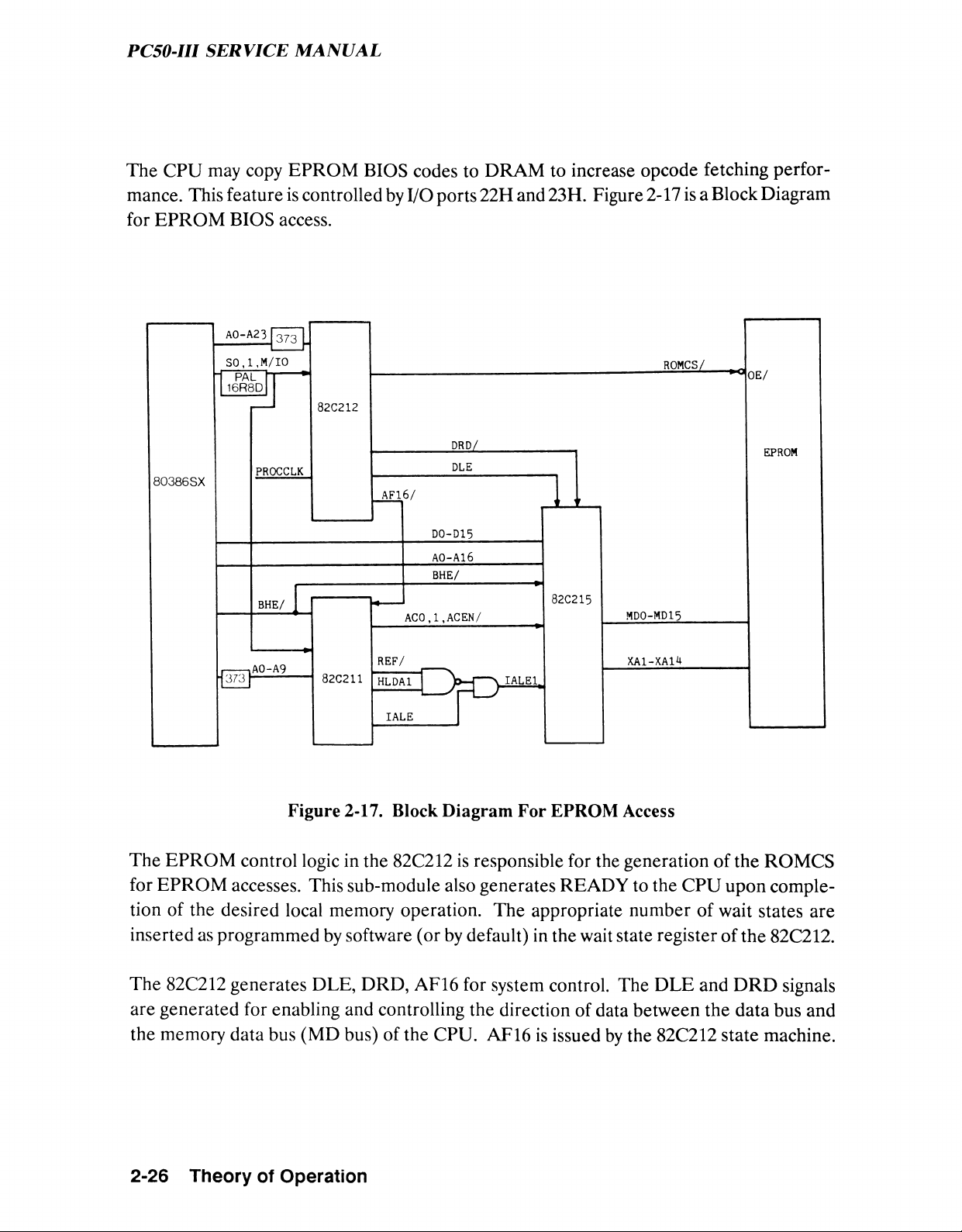
The CPU may copy EPROM BIOS codes to DRAM to increase opcode fetching perfor
mance. This feature is controlled by I/O ports 22H and 23H. Figure 2-17 is a Block Diagram
for EPROM BIOS access.
Figure 2-17. Block Diagram For EPROM Access
The EPROM control logic in the 82C212 is responsible for the generation of the ROMCS
for EPROM accesses. This sub-module also generates READY to the CPU upon comple
tion of the desired local memory operation. The appropriate number of wait states are
inserted as programmed by software (or by default) in the wait state register of the 82C212.
The 82C212 generates DLE, DRD, AF16 for system control. The DLE and DRD signals
are generated for enabling and controlling the direction of data between the data bus and
the memory data bus (MD bus) of the CPU. AF16 is issued by the 82C212 state machine.
2-26 Theory of Operation
Page 53
PC50-III SERVICE MANUAL
The external DRAM and I/O bus of MPC2386 work under AT bus cycle and are controlled
by XMEMR (XIOR) and XMEMW (XIOW). Both the on-board I/O access and the
interface card I/O access operate under AT bus cycle, and are controlled by XIOR and
XIOW signals. The transfer is 8 or 16 bits. When operating a 16-bit access to the 8 bit bus,
each CPU cycle needs to access the target twice.
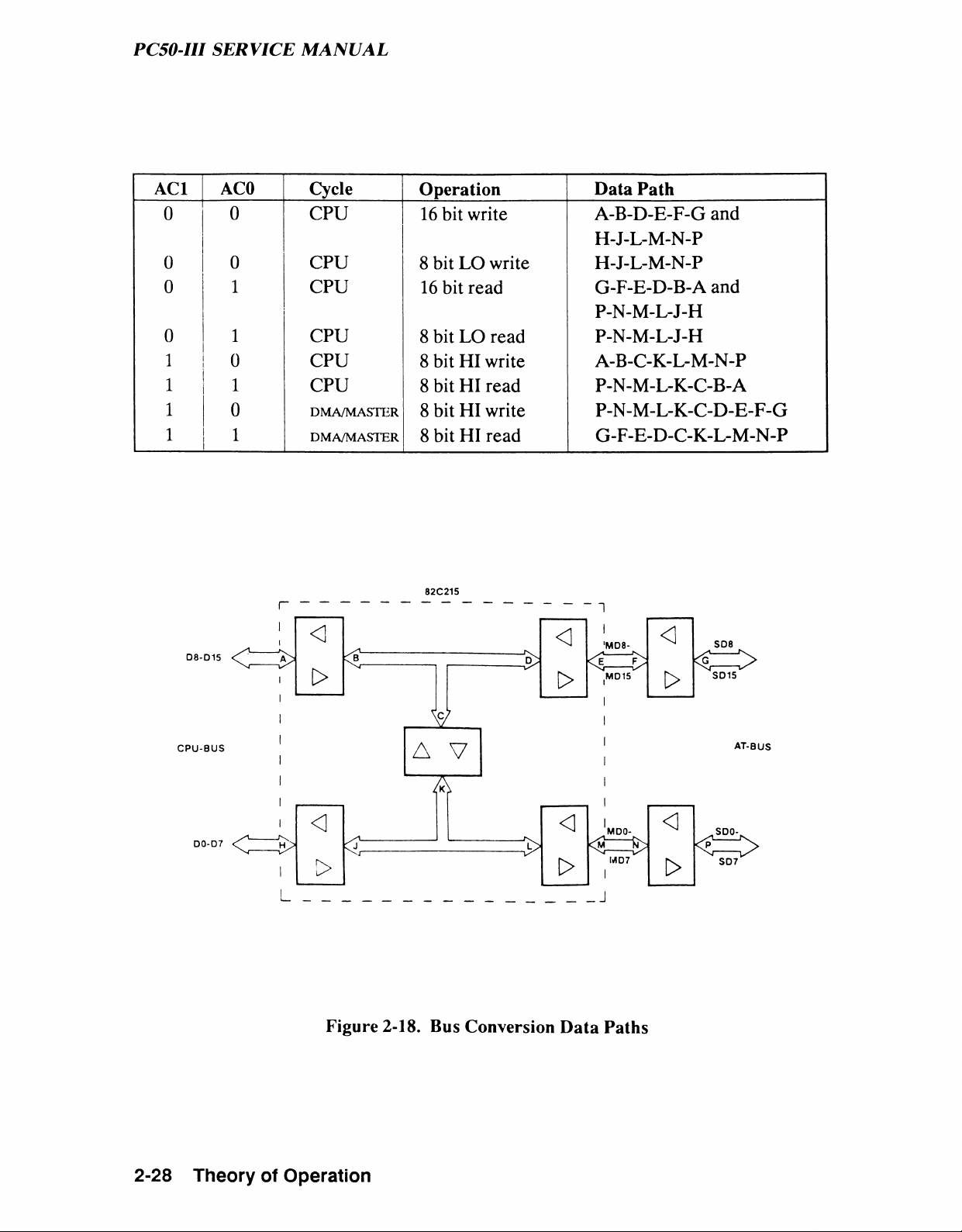
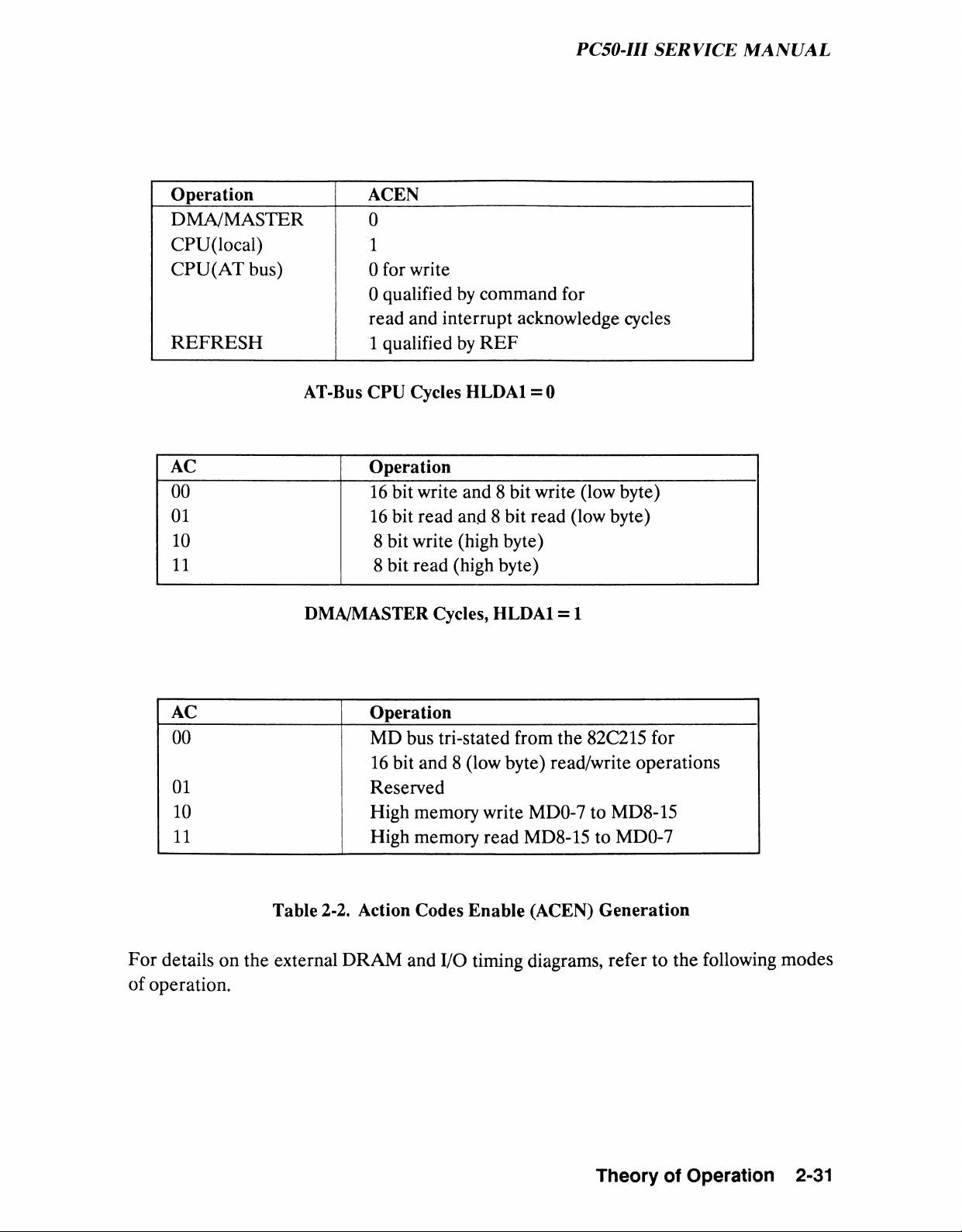
The 82C215 provides data bus conversion when the 16-bit CPU reads from or writes to 8
bit devices. It also provides bus conversion for DMA/Master cycles. There are six possible
cases, as shown in Figure 2-18. These conversions are controlled by the action codes which
are qualified by ACEN from the 82C211.
The AT state machine performs data conversion for CPU accesses to devices not on the
CPU or Memory Bus. The AT bus conversins are performed for 16 to 8 bit read or write
operations. 16-bit transfers to/from the CPU are broken into smaller 8-bit AT bus or
peripheral bus’ reads or writes. The action codes are generated as shown in Table 2-2 to
control the buffers in the 82C215. The action codes are in response to signals MEMCS16
and IOCS16.
2.2.4 External DRAM and I/O Access
Theory of Operation
2-27
Page 54
PC50-III SERVICE MANUAL
ACl
ACO
Cycle Operation Data Path
0
0
CPU
16 bit write A-B-D-E-F-G and
H-J-L-M-N-P
0 0
CPU
8 bit LO write
H-J-L-M-N-P
0 1
CPU
16 bit read
G-F-E-D-B-A and
P-N-M-L-J-H
0 1
CPU
8 bit LO read
P-N-M-L-J-H
1
o
CPU
8 bit HI write
A-B-C-K-L-M-N-P
1
1
CPU
8 bit HI read
P-N-M-L-K-C-B-A
1 0
DMA /M ASTER
8 bit HI write P-N-M-L-K-C-D-E-F-G
1 1
DMA /M ASTER
8 bit HI read
g -f -e -d -c -k -l -m -n -p
82C215
I
--------------------------------------------------
1
J
Figure 2-18. Bus Conversion Data Paths
2-28 Theory of Operation
Page 55
PC50-III SERVICE MANUAL
Figure 2-19. Normal Mode Local Cycle Followed By AT Bus Cycle (Ows, Ocd)
On the AT bus, certain slow peripherals require between 50 to 60 nanoseconds between
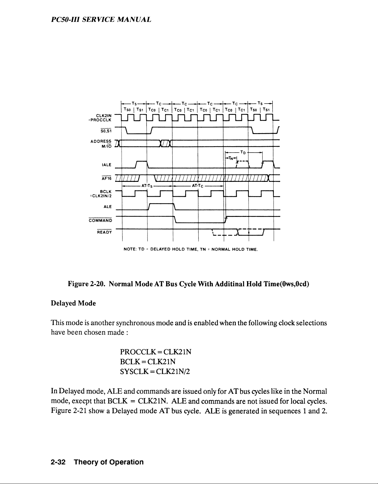
command going inactive to the next ALE going active, to provide sufficient data recovery
time. The sequence diagram in Figure 2-20 shows a Normal mode AT bus cycle with
additional hold time. The dotted IALE signal would have been valid, if the additional hold
time register had not been enabled in RA1. Instead, IALE is delayed by one T state of the
processor by asserting READY one T cycle later. The 82C212 provides an extended DLE
to the 82C215 in this mode, so that data is available to the CPU during write cycles. If this
mode was not invoked, then READY would have been asserted earlier as shown by the
dotted line. In Delayed mode, the 82C211 provides an extended data hold time. This
additional hold time can only be programmed in the Normal mode.
Theory of Operation 2-29
Page 56
PC50-IH SERVICE MANUAL
The system has 2 modes of operation for different CPU and AT bus clock selections :
• Normal Mode
• Delayed Mode
Normal Mode
This mode is enabled by default (without writing to the internal registers of the 82C211).
Under Normal m ode:
PROCLK = CLK21N
BCLK = CLK21N/2
SYSCLK = CLK21N/4
The CPU state machine clock and the AT bus state machine clock are derived from
CLK21N, a synchronous mode. ALE and commands (XMEMR, XMEMW, SIOR, SIOW)
are issued only for AT bus cycles and not for local cycles. If activated by default, I/O cycles
will have one command delay. 8-bit AT memory cycles will have 4 wait states, while 16- bit
AT memory cycles will have 1 wait state.
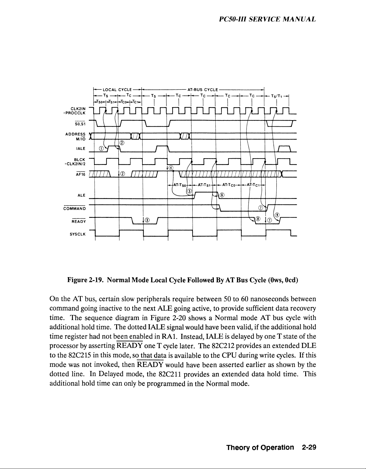
Figure 2-19 shows the sequence diagram of a Normal mode local cycle followed by an AT
bus cycle with zero wait states (0 W.S.) and zero command delay (0 C.D.) In sequences 1
and 2, IALE is generated from CLK21N. AF16 is sampled to be low in sequence 2. ALE
and AT bus commands (XIOR, XIOW, XMEMR, MEMW) are not generated since it is a
local cycle. For a zero wait state cycle, READY is sampled low by the 80386SX CPU in
sequence 3 and the cycle is terminated. For the AT bus cycle, AF16 is sampled high in
sequence 4. Control is transferred to the AT bus state machine. BCLK then generates the
AT bus states. ALE is generated in sequences 5 and 6. The AT bus command is generated
in sequences 6 and 7, for zero command delays programmed in the 82C211. For a zero wait
state cycle, READY is asserted low as shown in sequences 8 and 9, to be sampled by the
CPU in sequence 7. This terminates the AT bus cycle.
2-30 Theory of Operation
Page 57
PC50-IU SERVICE MANUAL
Operation
ACEN
DMA/MASTER
0
CPU(local)
1
CPU(AT bus)
0 for write
0 qualified by command for
read and interrupt acknowledge cycles
REFRESH
1 qualified by REF
AT-Bus CPU Cycles HLDA1 = 0
AC Operation
00
16 bit write and 8 bit write (low byte)
01
16 bit read and 8 bit read (low byte)
10
8 bit write (high byte)
11
8 bit read (high byte)
DMA/MASTER Cycles, HLDA1 = 1
AC Operation
00
MD bus tri-stated from the 82C215 for
16 bit and 8 (low byte) read/write operations
01
Reserved
10
High memory write MDO-7 to MD8-15
11
High memory read MD8-15 to MDO-7
Table 2-2. Action Codes Enable (ACEN) Generation
For details on the external DRAM and I/O timing diagrams, refer to the following modes
of operation.
Theory of Operation 2-31
Page 58
PC50-IU SERVICE MANUAL
Figure 2-20. Normal Mode AT Bus Cycle With Additinal Hold Time(0ws,0cd)
Delayed Mode
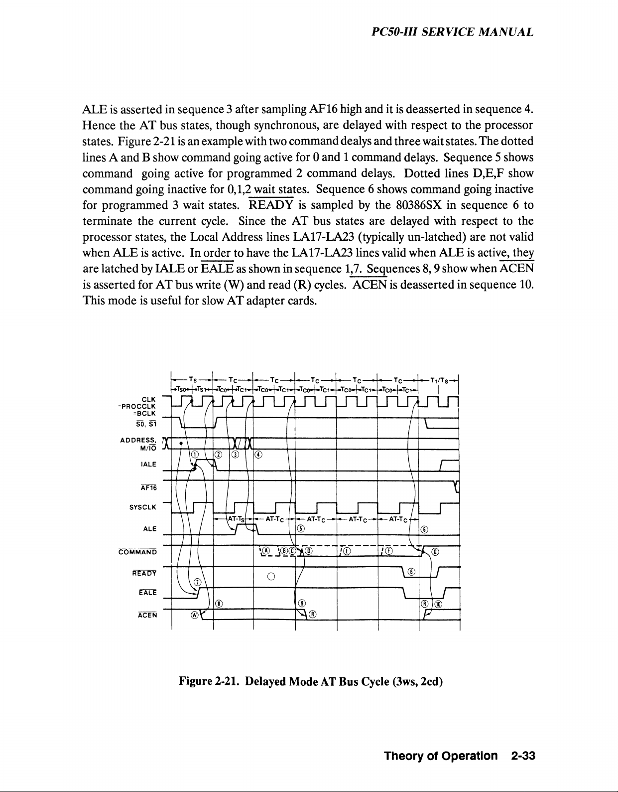
This mode is another synchronous mode and is enabled when the following clock selections
have been chosen made :
PROCCLK = CLK21N
BCLK = CLK21N
SYSCLK = CLK21N/2
In Delayed mode, ALE and commands are issued only for AT bus cycles like in the Normal
mode, execpt that BCLK = CLK21N. ALE and commands are not issued for local cycles.
Figure 2-21 show a Delayed mode AT bus cycle. ALE is generated in sequences 1 and 2.
2-32 Theory of Operation
Page 59
PC50-III SERVICE MANUAL
ALE is asserted in sequence 3 after sampling AF16 high and it is deasserted in sequence 4.
Hence the AT bus states, though synchronous, are delayed with respect to the processor
states. Figure 2-21 is an example with two command dealys and three wait states. The dotted
lines A and B show command going active for 0 and 1 command delays. Sequence 5 shows
command going active for programmed 2 command delays. Dotted lines D,E,F show
command going inactive for 0,1,2 wait states. Sequence 6 shows command going inactive
for programmed 3 wait states. READY is sampled by the 80386SX in sequence 6 to
terminate the current cycle. Since the AT bus states are delayed with respect to the
processor states, the Local Address lines LA17-LA23 (typically un-latched) are not valid
when ALE is active. In order to have the LA17-LA23 lines valid when ALE is active, they
are latched by LALE or EALE as shown in sequence 1,7. Sequences 8,9 show when ACEN
is asserted for AT bus write (W) and read (R) cycles. ACEN is deasserted in sequence 10.
This mode is useful for slow AT adapter cards.
Figure 2-21. Delayed M ode AT Bus Cycle (3ws, 2cd)
Theory of Operation
2-33
Page 60
PC50-III SERVICE MANUAL
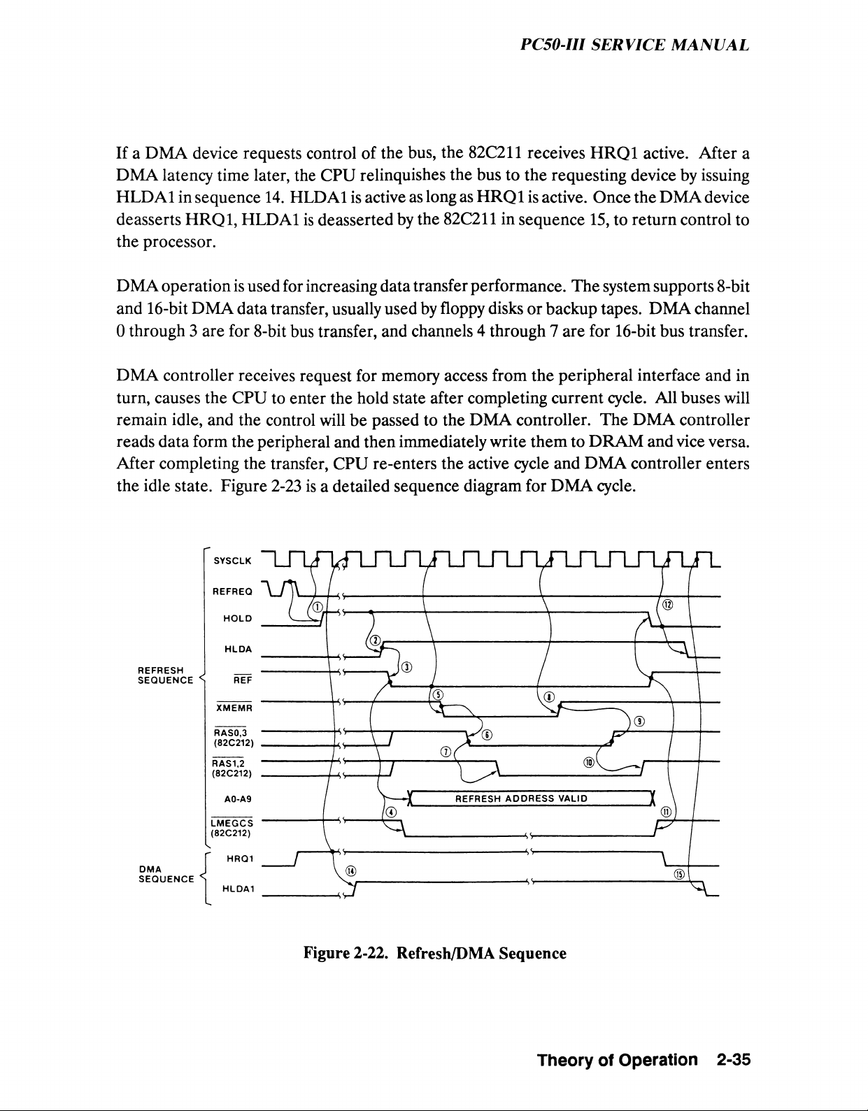
2.2.5 DRAM Refresh and DMA Access
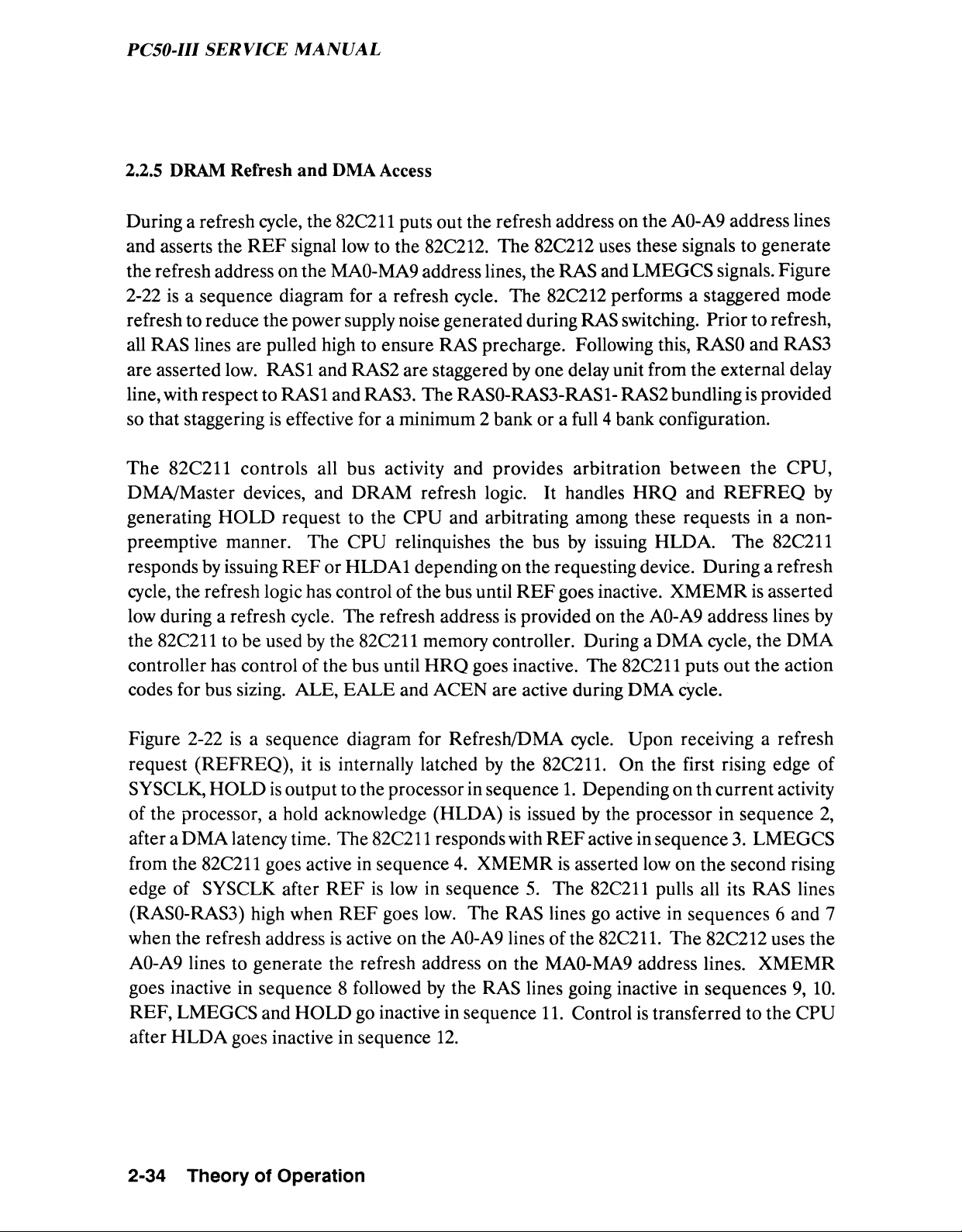
During a refresh cycle, the 82C211 puts out the refresh address on the A0-A9 address lines
and asserts the REF signal low to the 82C212. The 82C212 uses these signals to generate
the refresh address on the MA0-MA9 address lines, the RAS and LMEGCS signals. Figure
2-22 is a sequence diagram for a refresh cycle. The 82C212 performs a staggered mode
refresh to reduce the power supply noise generated during RAS switching. Prior to refresh,
all RAS lines are pulled high to ensure RAS precharge. Following this, RASO and RAS3
are asserted low. RAS1 and RAS2 are staggered by one delay unit from the external delay
line, with respect to RAS1 and RAS3. The RAS0-RAS3-RAS1- RAS2 bundling is provided
so that staggering is effective for a minimum 2 bank or a full 4 bank configuration.
The 82C211 controls all bus activity and provides arbitration between the CPU,
DMA/Master devices, and DRAM refresh logic. It handles HRQ and REFREQ by
generating HOLD request to the CPU and arbitrating among these requests in a non-
preemptive manner. The CPU relinquishes the bus by issuing HLDA. The 82C211
responds by issuing REF or HLDA1 depending on the requesting device. During a refresh
cycle, the refresh logic has control of the bus until REF goes inactive. XMEMR is asserted
low during a refresh cycle. The refresh address is provided on the A0-A9 address lines by
the 82C211 to be used by the 82C211 memory controller. During a DMA cycle, the DMA
controller has control of the bus until HRQ goes inactive. The 82C211 puts out the action
codes for bus sizing. ALE, EALE and ACEN are active during DMA cycle.
Figure 2-22 is a sequence diagram for Refresh/DMA cycle. Upon receiving a refresh
request (REFREQ), it is internally latched by the 82C211. On the first rising edge of
SYSCLK, HOLD is output to the processor in sequence 1. Depending on th current activity
of the processor, a hold acknowledge (HLDA) is issued by the processor in sequence 2,
after a DMA latency time. The 82C211 responds with REF active in sequence 3. LMEGCS
from the 82C211 goes active in sequence 4. XMEMR is asserted low on the second rising
edge of SYSCLK after REF is low in sequence 5. The 82C211 pulls all its RAS lines
(RAS0-RAS3) high when REF goes low. The RAS lines go active in sequences 6 and 7
when the refresh address is active on the A0-A9 lines of the 82C211. The 82C212 uses the
A0-A9 lines to generate the refresh address on the MA0-MA9 address lines. XMEMR
goes inactive in sequence 8 followed by the RAS lines going inactive in sequences 9, 10.
REF, LMEGCS and HOLD go inactive in sequence 11. Control is transferred to the CPU
after HLDA goes inactive in sequence 12.
2-34 Theory of Operation
Page 61
PC50-UI SERVICE MANUAL
If a DMA device requests control of the bus, the 82C211 receives HRQ1 active. After a
DMA latency time later, the CPU relinquishes the bus to the requesting device by issuing
HLDA1 in sequence 14. HLDA1 is active as long as HRQ1 is active. Once the DMA device
deasserts HRQ1, HLDA1 is deasserted by the 82C211 in sequence 15, to return control to
the processor.
DMA operation is used for increasing data transfer performance. The system supports 8-bit
and 16-bit DMA data transfer, usually used by floppy disks or backup tapes. DMA channel
0 through 3 are for 8-bit bus transfer, and channels 4 through 7 are for 16-bit bus transfer.
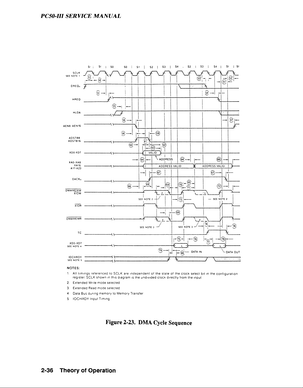
DMA controller receives request for memory access from the peripheral interface and in
turn, causes the CPU to enter the hold state after completing current cycle. All buses will
remain idle, and the control will be passed to the DMA controller. The DMA controller
reads data form the peripheral and then immediately write them to DRAM and vice versa.
After completing the transfer, CPU re-enters the active cycle and DMA controller enters
the idle state. Figure 2-23 is a detailed sequence diagram for DMA cycle.
Figure 2-22. Refresh/DMA Sequence
Theory of Operation 2-35
Page 62
PC50-III SERVICE MANUAL
SI i SI I so so
SI
S2 | S3
S4 j S2 | S3
S4 | SI | SI
NOTES:
1. All timin gs referenced to SCLK are indep end ent of the state of the clock select bit in the c onf igu rati on
register. SCLK shown in this diagram is the undiv ided cloc k dir ectly from the input
2. Extended Write mode selected
3. Extended Read mode selected
4 Data Bus during me mory to Memor y Transfer
5. IOCHRDY Input Ti ming
Figure 2-23. DMA Cycle Sequence
2-36 Theory of Operation
Page 63
PC50-III SERVICE MANUAL
2.2.6 Interrupt
The system support both software-generated and hardware-generated interrupts.
Software-generated interrupt function allows the programmers to use BIOS and DOS
utilities. Hardware-generated interrupts allows the interface to request the system to
execute pre-set functions.
2.2.7 Keyboard Controller
Keyboard controller is the interface between the main system and the keyboard. The
keyboard controller (8042) communicates with CPU per 8-bit parallel transfer, and with
the keyboard per 11-bit serial transfer.
The 8042 generates KBCLK to signal a synchronous keyboard data transfer. Before sending
data to the keyboard, the CPU must wait until the keyboard input buffer is empty. When
entering data from keyboard, the key codes will be sent to the 8042. The 8042 in turn
generates INT 1 to request execution of the data transfer.
2.2.8 Parity Generation/Detection
For local RAM write cycles, the 82C215 generates even parity for each of the two bytes of
data. These valid even parity bits are written to the parity bits MPO, MP1 in the local
DRAMs. During a local RAM read cycle, the 82C215 checks for even parity for each MD
bytes read. If the parity is detected as being odd, the 82C215 flags a parity error on the
PARERR output line to 82C211.
Theory of Operation 2-37
Page 64
PC50-III SERVICE MANUAL
2.2.9 Port B And NMI Generation
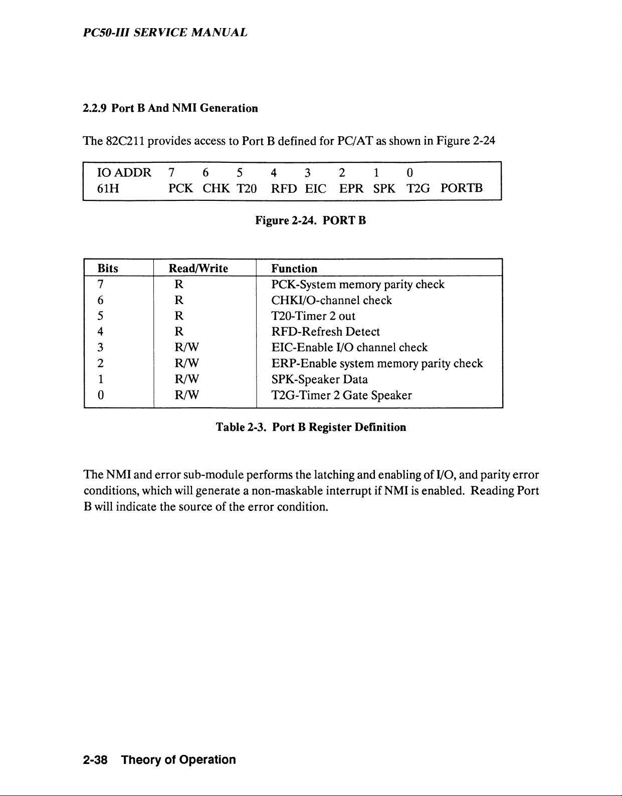
The 82C211 provides access to Port B defined for PC/AT as shown in Figure 2-24
IO ADDR 7
6 5
4
3
2 1
0
61H
PCK
CHK T20
RFD EIC
EPR SPK
T2G PORTB
Figure 2-24. PORT B
Bits Read/Write Function
7
R
PCK-System memory parity check
6
R
CHKI/O-channel check
5
R
T20-Timer 2 out
4 R
RFD-Refresh Detect
3
R/W
EIC-Enable I/O channel check
2 R/W ERP-Enable system memory parity check
1 R/W
SPK-Speaker Data
0
R/W
T2G-Timer 2 Gate Speaker
Table 2-3. Port B Register Definition
The NMI and error sub-module performs the latching and enabling of I/O, and parity error
conditions, which will generate a non-maskable interrupt if NMI is enabled. Reading Port
B will indicate the source of the error condition.
2-38
Theory of Operation
Page 65
PC50-III SERVICE MANUAL
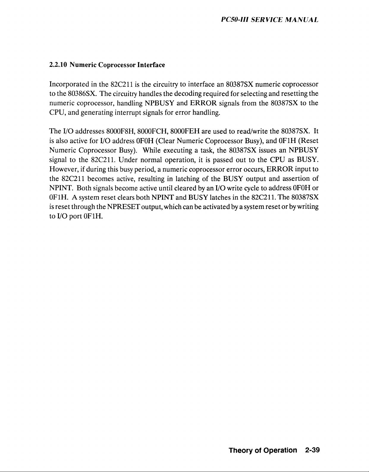
2.2.10 Numeric Coprocessor Interface
Incorporated in the 82C211 is the circuitry to interface an 80387SX numeric coprocessor
to the 80386SX. The circuitry handles the decoding required for selecting and resetting the
numeric coprocessor, handling NPBUSY and ERROR signals from the 80387SX to the
CPU, and generating interrupt signals for error handling.
The I/O addresses 8000F8H, 8000FCH, 8000FEH are used to read/write the 80387SX. It
is also active for I/O address 0F0H (Clear Numeric Coprocessor Busy), and 0F1H (Reset
Numeric Coprocessor Busy). While executing a task, the 80387SX issues an NPBUSY
signal to the 82C211. Under normal operation, it is passed out to the CPU as BUSY.
However, if during this busy period, a numeric coprocessor error occurs, ERROR input to
the 82C211 becomes active, resulting in latching of the BUSY output and assertion of
NPINT. Both signals become active until cleared by an I/O write cycle to address 0F0H or
0F1H. A system reset clears both NPINT and BUSY latches in the 82C211. The 80387SX
is reset through the NPRESET output, which can be activated by a system reset or by writing
to I/O port 0F1H.
Theory of Operation 2-39
Page 66

Page 67
PC50-III SERVICE MANUAL
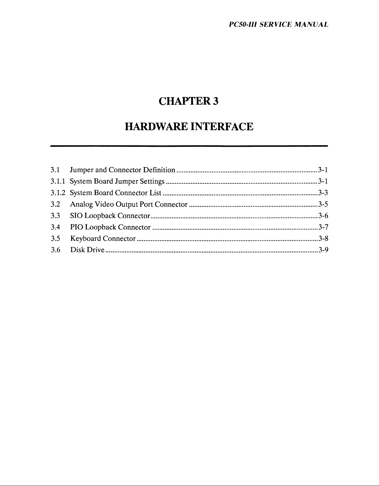
CHAPTER 3
HARDWARE INTERFACE
3.1 Jumper and Connector Definition.............................................................................3-1
3.1.1 System Board Jumper Settings
..................................................................................
3-1
3.1.2 System Board Connector List.................................................................................... 3-3
3.2 Analog Video Output Port Connector......................................................................3-5
3.3 SIO Loopback Connector...........................................................................................3-6
3.4 PIO Loopback Connector..........................................................................................3-7
3.5 Keyboard Connector...................................................................................................3-8
3.6 Disk Drive....................................................................................................................3-9
Page 68

Page 69
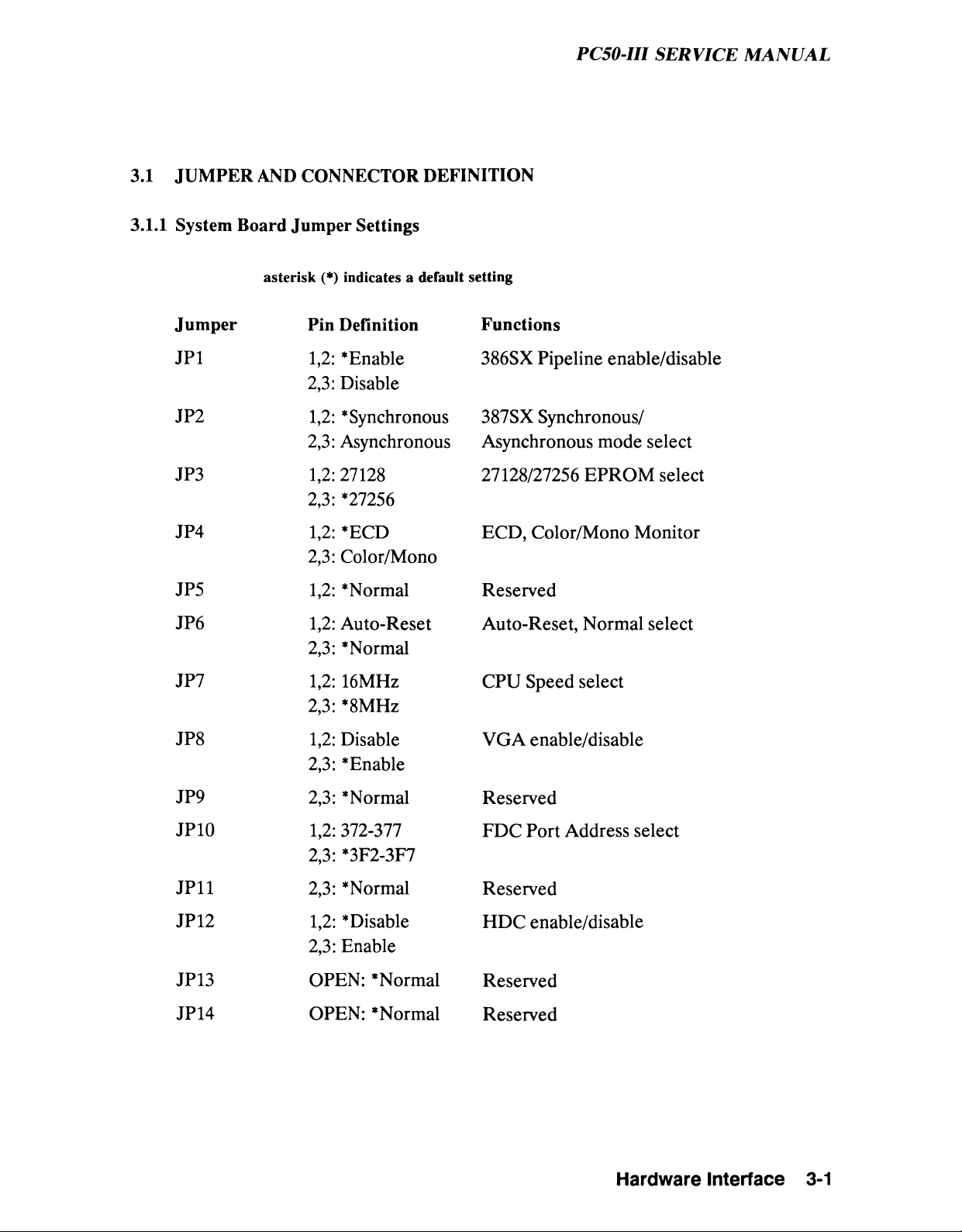
3.1 JUMPER AND CONNECTOR DEFINITION
3.1.1 System Board Jumper Settings
asterisk 0") indicates a default setting
PC50-IU SERVICE MANUAL
Jumper Pin Definition
JP1
1,2: ‘Enable
2,3: Disable
JP2
1,2: ‘Synchronous
2,3: Asynchronous
JP3 1,2: 27128
2,3: *27256
JP4
1,2: *ECD
2,3: Color/Mono
JP5
JP6
1,2: ‘Normal
1,2: Auto-Reset
2,3: ‘Normal
JP7
1,2: 16MHz
2,3: *8MHz
JP8
1,2: Disable
2,3: ‘Enable
Functions
386SX Pipeline enable/disable
387SX Synchronous/
Asynchronous mode select
27128/27256 EPROM select
ECD, Color/Mono Monitor
Reserved
Auto-Reset, Normal select
CPU Speed select
VGA enable/disable
JP9
JP10
2,3: ‘Normal
1,2:372-377
2,3: ‘3F2-3F7
JP11
2,3: ‘Normal
JP12 1,2: ‘Disable
2,3: Enable
JP13
OPEN: ‘Normal
JP14 OPEN: ‘Normal
Reserved
FDC Port Address select
Reserved
HDC enable/disable
Reserved
Reserved
Hardware Interface
3-1
Page 70
PC50-III SERVICE MANUAL
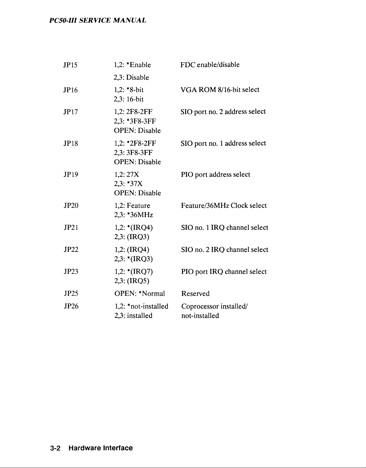
JP15
1,2: ‘Enable
2,3: Disable
JP16
1,2: * 8-bit
2,3:16-bit
JP17
1,2: 2F8-2FF
2,3: ‘3F8-3FF
OPEN: Disable
JP18
1,2: ‘2F8-2FF
2,3: 3F8-3FF
OPEN: Disable
JP19
1,2: 27X
2,3: *37X
OPEN: Disable
JP20
1,2: Feature
2,3: *36MHz
JP21 1,2: *(IRQ4)
2,3: (IRQ3)
JP22 1,2: (IRQ4)
2,3: *(IRQ3)
JP23
1,2: *(IRQ7)
2,3: (IRQ5)
JP25
OPEN: ‘Normal
JP26
1,2: * not-installed
2,3: installed
FDC enable/disable
VGA ROM 8/16-bit select
SIO port no. 2 address select
SIO port no. 1 address select
PIO port address select
Feature/36MHz Clock select
SIO no. 1 IRQ channel select
SIO no. 2 IRQ channel select
PIO port IRQ channel select
Reserved
Coprocessor installed/
not-installed
3-2
Hardware Interface
Page 71
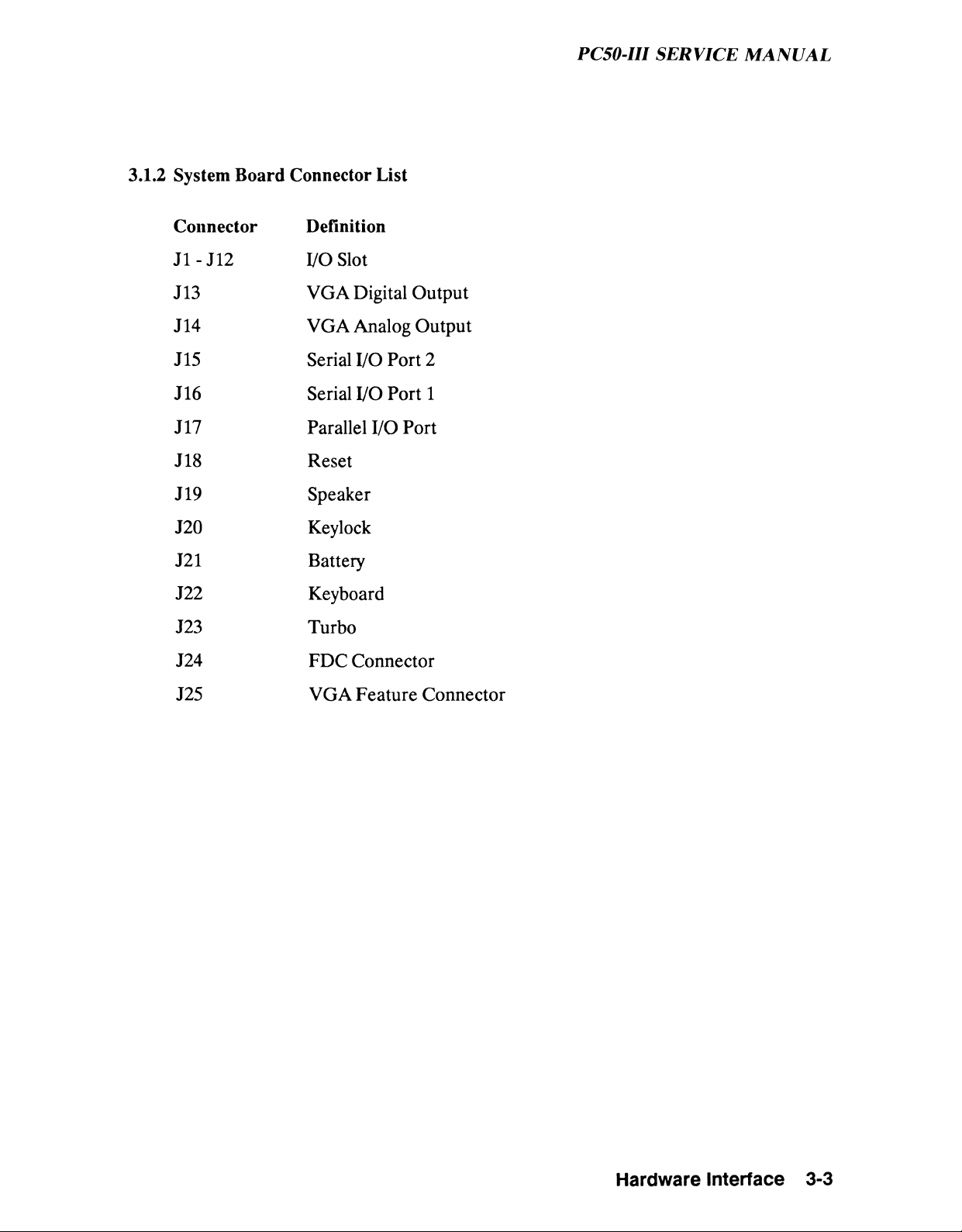
3.1.2 System Board Connector List
PC50-III SERVICE MANUAL
Connector
J1-J12
J13
J14
J15
J16 Serial I/O Port 1
J17
J18
J19
J20 Keylock
J21
J22
J23
J24
Definition
I/O Slot
VGA Digital Output
VGA Analog Output
Serial I/O Port 2
Parallel I/O Port
Reset
Speaker
Battery
Keyboard
Turbo
FDC Connector
J25
VGA Feature Connector
Hardware Interface
3-3
Page 72
PC50-III SERVICE MANUAL
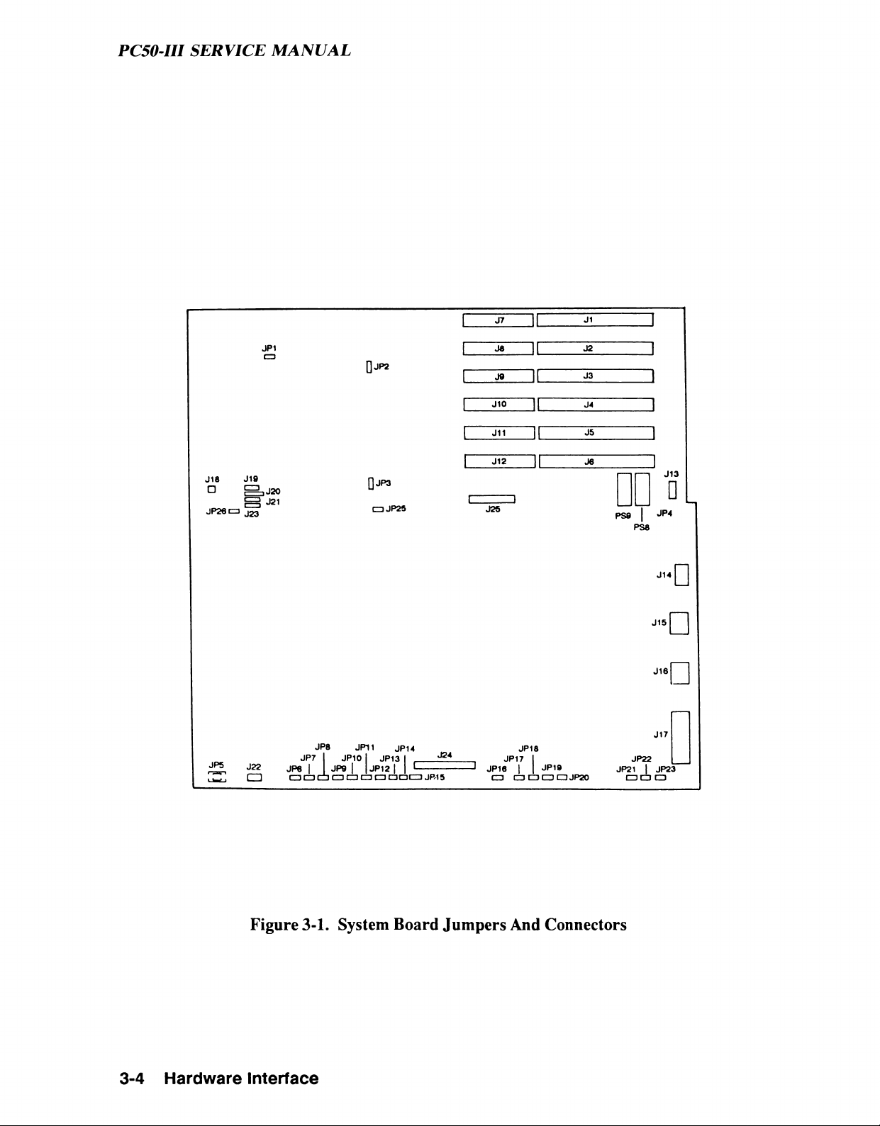
Figure 3-1. System Board Jumpers And Connectors
3-4 Hardware Interface
Page 73
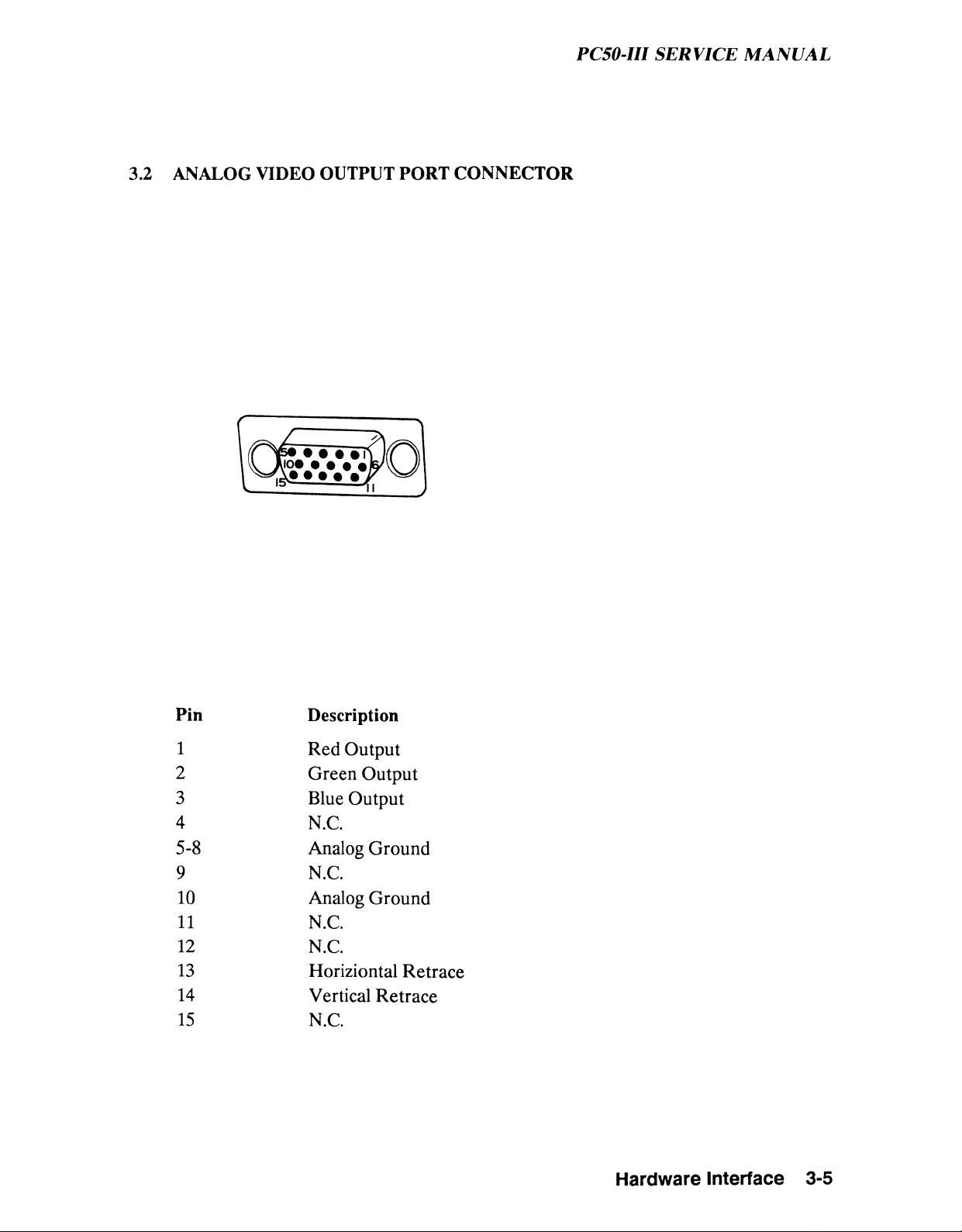
ANALOG VIDEO OUTPUT PORT CONNECTOR
PC50-1II SERVICE MANUAL
Pin
1
2
3
4
5-8
9
10
11
12
13
14
15
Description
Red Output
Green Output
Blue Output
N.C.
Analog Ground
N.C.
Analog Ground
N.C.
N.C.
Horiziontal Retrace
Vertical Retrace
N.C.
Hardware Interface
3-5
Page 74
PC50-IU SERVICE MANUAL
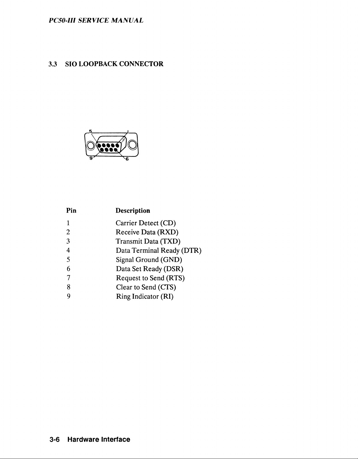
3.3 SIO LOOPBACK CONNECTOR
Pin Description
1
2
3
4
5
6
7
8
9
Carrier Detect (CD)
Receive Data (RXD)
Transmit Data (TXD)
Data Terminal Ready (DTR)
Signal Ground (GND)
Data Set Ready (DSR)
Request to Send (RTS)
Clear to Send (CTS)
Ring Indicator (RI)
3-6
Hardware Interface
Page 75
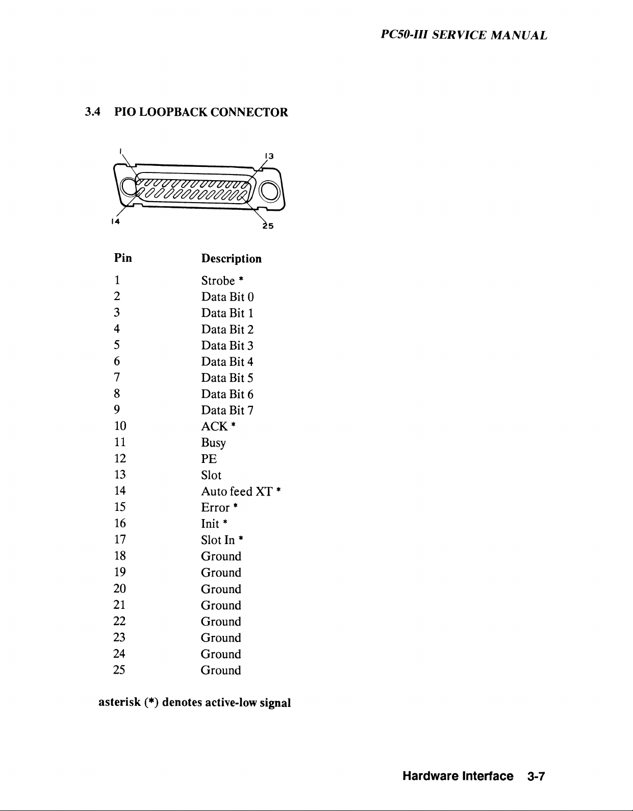
3.4 PIO LOOPBACK CONNECTOR
14
PC50-III SERVICE MANUAL
Pin
1
2
3
4
5
6
7
8
9
10
11
12
13
14
15
16
17
18
19
20
21
22
23
24
25
Description
Strobe *
Data Bit 0
Data Bit 1
Data Bit 2
Data Bit 3
Data Bit 4
Data Bit 5
Data Bit 6
Data Bit 7
ACK*
Busy
PE
Slot
Auto feed XT
Error *
Init *
Slot In *
Ground
Ground
Ground
Ground
Ground
Ground
Ground
Ground
asterisk (*) denotes active-low signal
Hardware Interface
3-7
Page 76
PC50-III SERVICE MANUAL
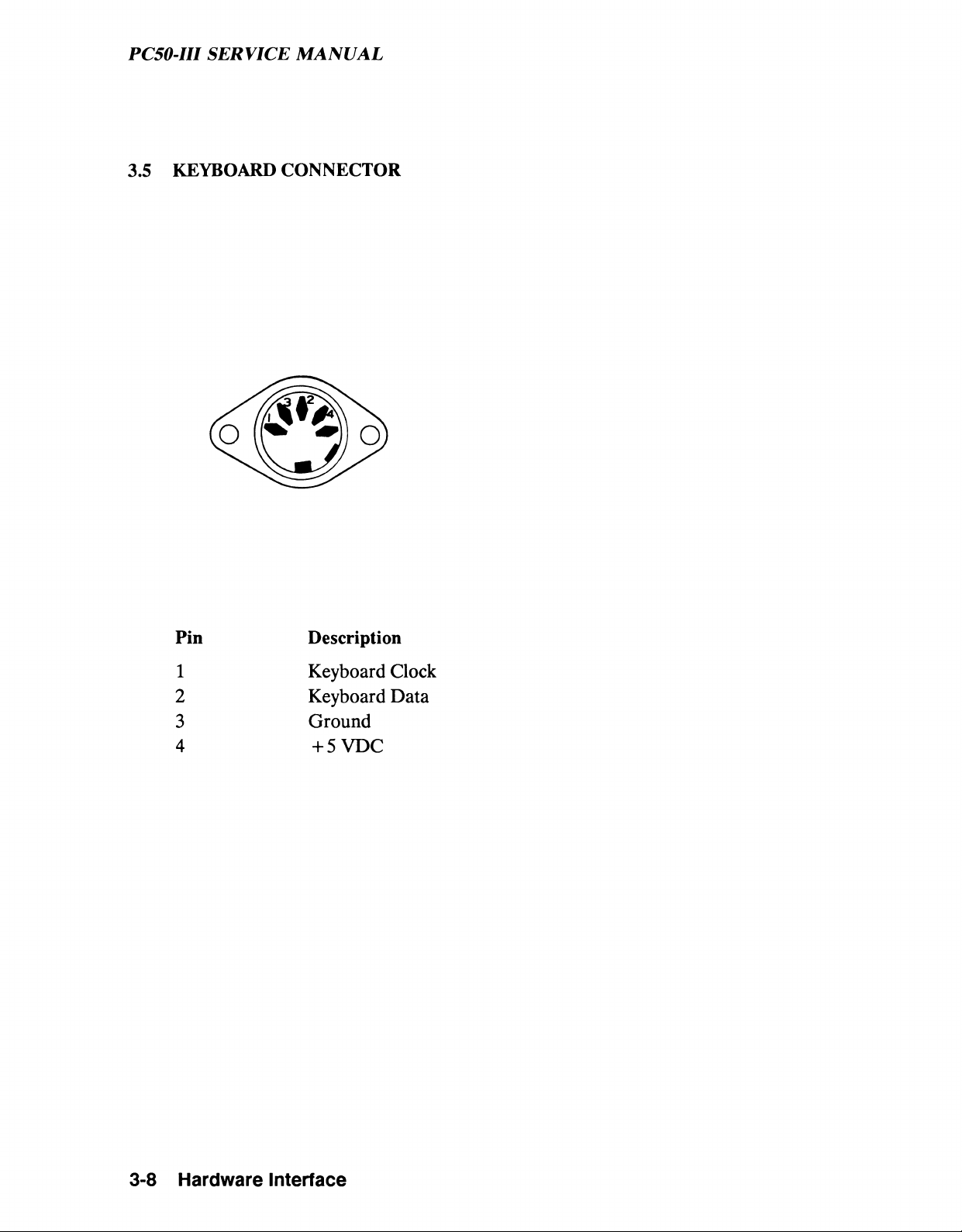
3.5 KEYBOARD CONNECTOR
Pin Description
1 Keyboard Clock
2 Keyboard Data
3 Ground
4 + 5 VDC
3-8
Hardware Interface
Page 77
PC50-III SERVICE MANUAL
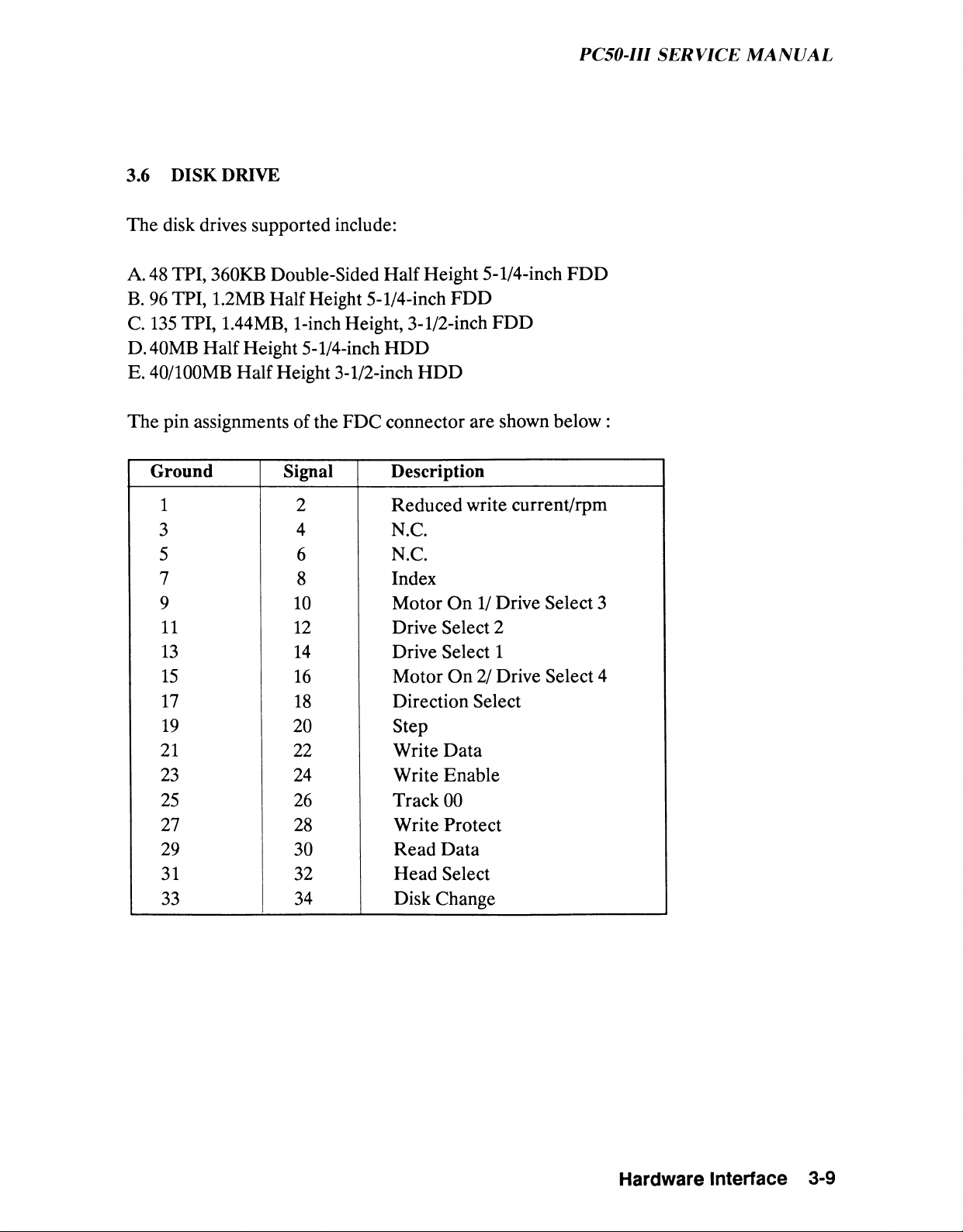
3.6 DISKDRIVE
The disk drives supported include:
A. 48 TPI, 360KB Double-Sided Half Height 5-1/4-inch FDD
B. 96 TPI, 1.2MB Half Height 5-1/4-inch FDD
C. 135 TPI, 1.44MB, 1-inch Height, 3-1/2-inch FDD
D. 40MB Half Height 5-1/4-inch HDD
E. 40/100MB Half Height 3-1/2-inch HDD
The pin assignments of the FDC connector are shown below:
Ground
Signal
Description
1 2 Reduced write current/rpm
3
4
N.C.
5 6 N.C.
7
8
Index
9
10
Motor On 1/ Drive Select 3
11 12
Drive Select 2
13 14
Drive Select 1
15
16
Motor On 2/ Drive Select 4
17
18
Direction Select
19
20 Step
21
22
Write Data
23 24
Write Enable
25 26 Track 00
27
28 Write Protect
29 30 Read Data
31 32
Head Select
33
34
Disk Change
Hardware Interface
3-9
Page 78

Page 79
PC50-III SERVICE MANUAL
CHAPTER 4
REMOVING COMPONENTS
4.1 Removing the System Unit Cover..............................................................................4-1
4.2 Removing an Option Board....................................................................................... 4-3
4.3 Removing Disk Drives................................................................................................4-4
4.3.1 5-1/4-inch Disk Drive.................................................................................................4-4
4.3.2 3-1/2-inch Floppy Disk Drive..................................................................................... 4-5
4.3.3 3-1/2-inch Hard Disk Drive........................................................................................ 4-6
4.4 Removing DRAM Modules....................................................................................... 4-8
4.5 Removing Numeric Coprocessor...............................................................................4-9
4.6 Removing Power Supply...........................................................................................4-11
4.7 Removing System Board...........................................................................................4-12
Page 80

Page 81
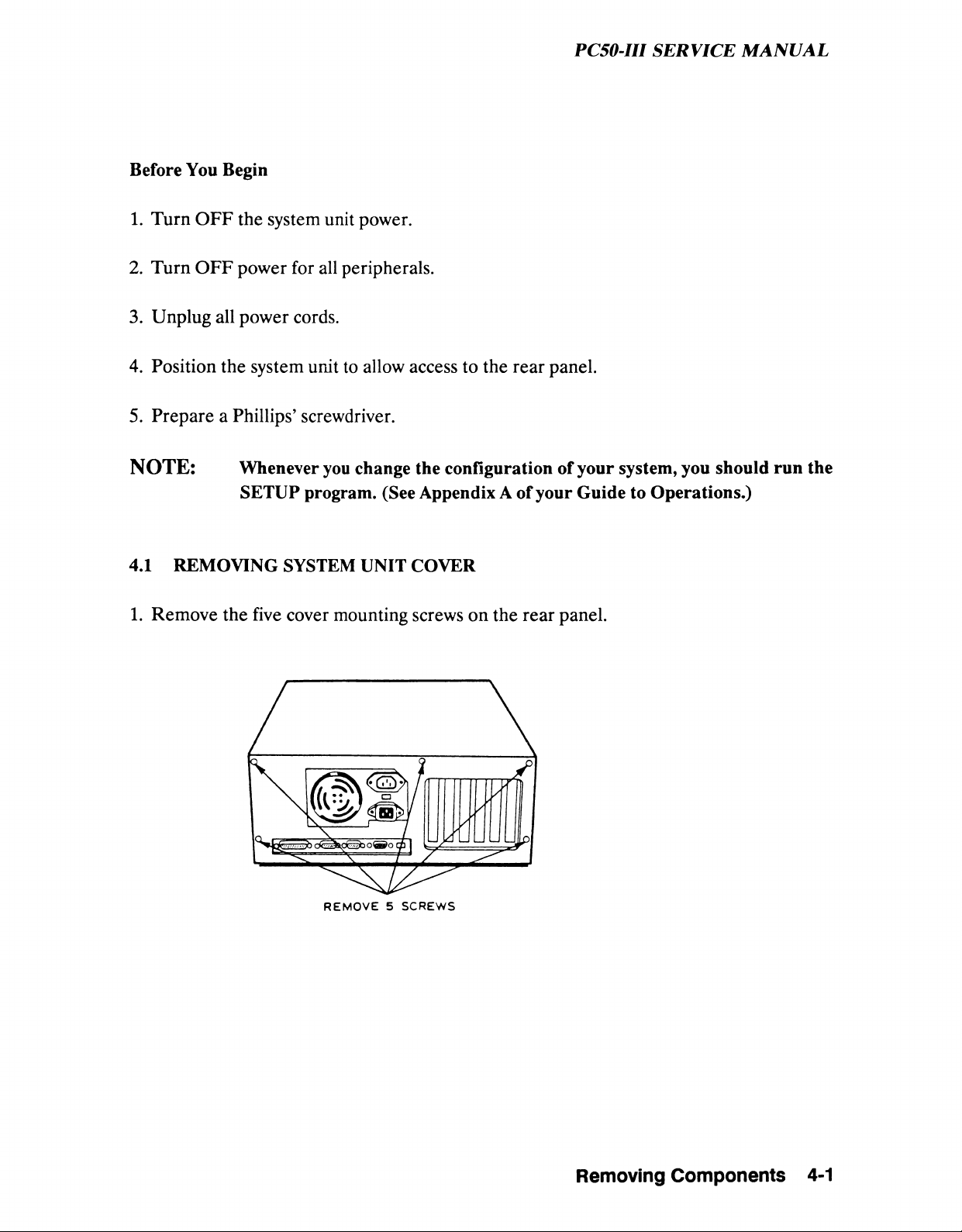
PC50-IH SERVICE MANUAL
Before You Begin
1. Turn OFF the system unit power.
2. Turn OFF power for all peripherals.
3. Unplug all power cords.
4. Position the system unit to allow access to the rear panel.
5. Prepare a Phillips’ screwdriver.
NOTE: Whenever you change the configuration of your system, you should run the
SETUP program. (See Appendix A of your Guide to Operations.)
4.1 REMOVING SYSTEM UNIT COVER
1. Remove the five cover mounting screws on the rear panel.
REMOVE 5 SCREWS
Removing Components 4-1
Page 82
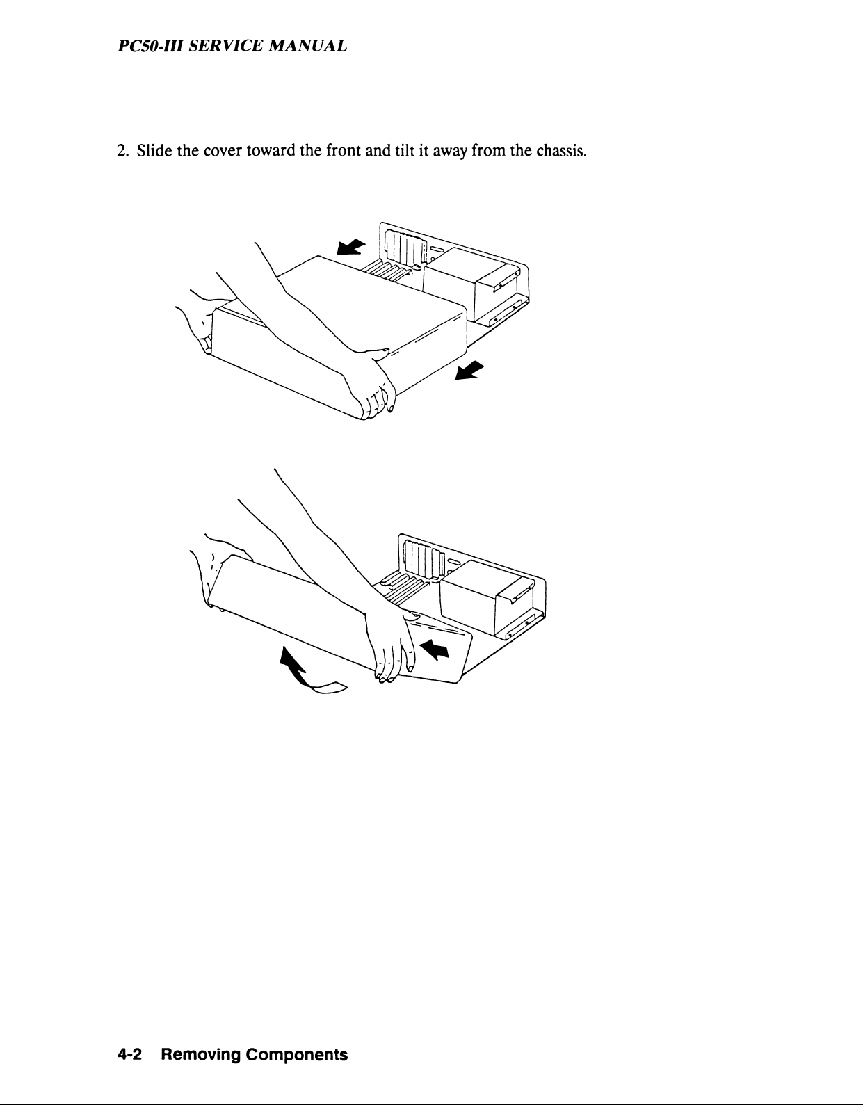
PC50-III SERVICE MANUAL
2. Slide the cover toward the front and tilt it away from the chassis.
4-2 Removing Components
Page 83
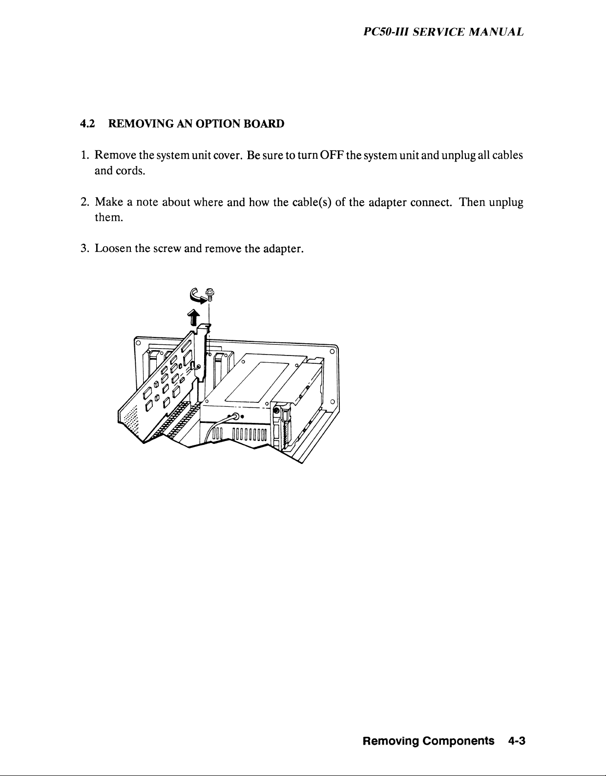
PC50-III SERVICE MANUAL
4.2 REMOVING AN OPTION BOARD
1. Remove the system unit cover. Be sure to turn OFF the system unit and unplug all cables
and cords.
2. Make a note about where and how the cable(s) of the adapter connect. Then unplug
them.
3. Loosen the screw and remove the adapter.
Removing Components
4-3
Page 84
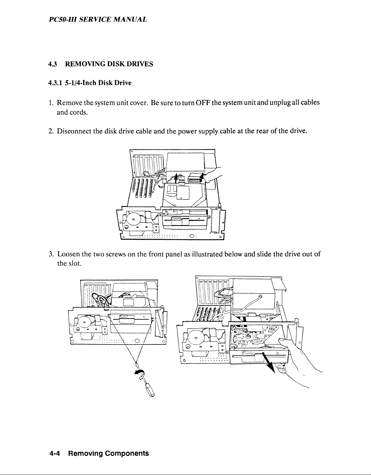
PC50-III SERVICE MANUAL
43 REMOVING DISK DRIVES
4.3.1 5-1/4-Inch Disk Drive
1. Remove the system unit cover. Be sure to turn OFF the system unit and unplug all cables
and cords.
2. Disconnect the disk drive cable and the power supply cable at the rear of the drive.
3. Loosen the two screws on the front panel as illustrated below and slide the drive out of
the slot.
4-4 Removing Components
Page 85
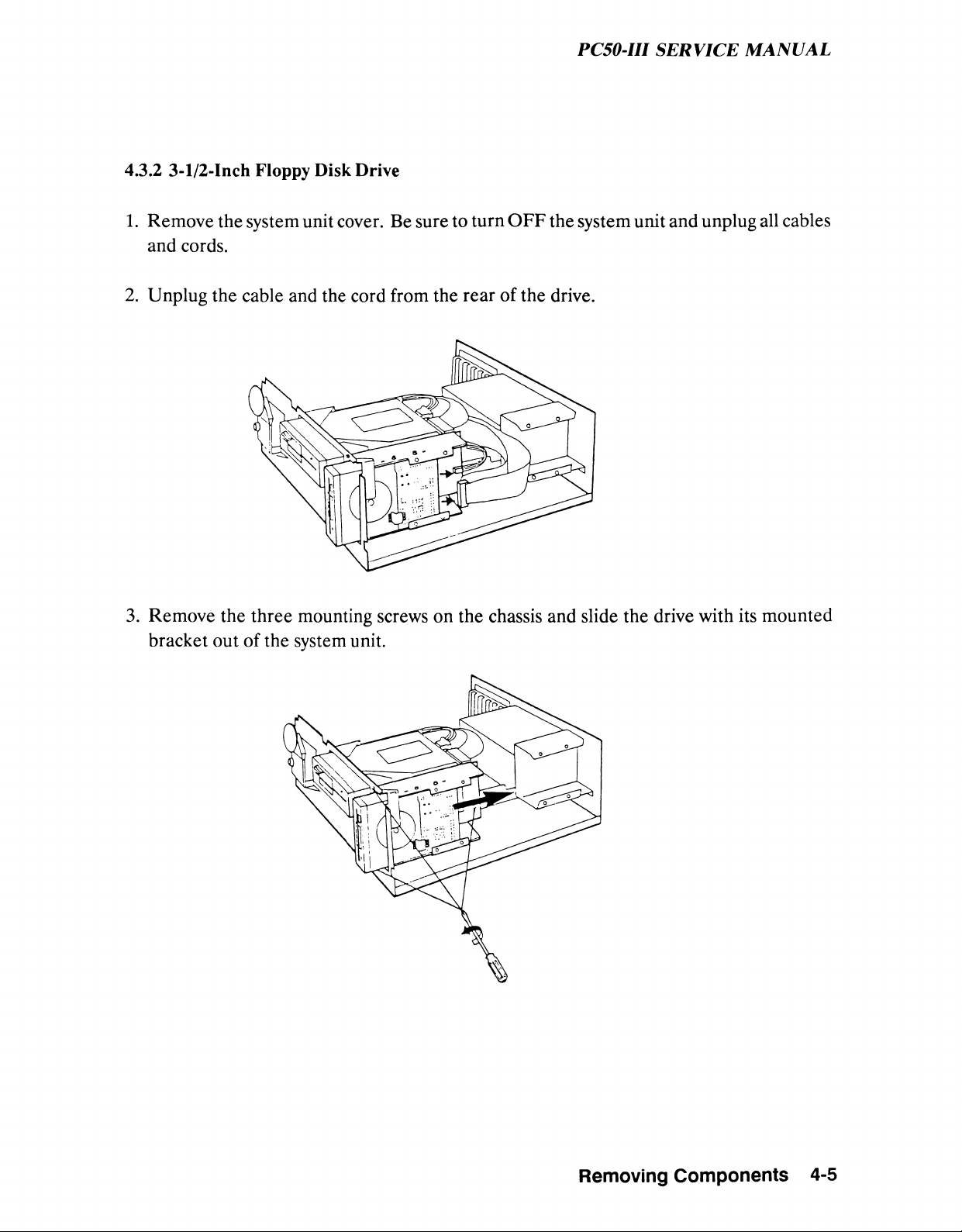
PC50-III SERVICE MANUAL
4.3.2 3-1/2-Inch Floppy Disk Drive
1. Remove the system unit cover. Be sure to turn OFF the system unit and unplug all cables
and cords.
2. Unplug the cable and the cord from the rear of the drive.
3. Remove the three mounting screws on the chassis and slide the drive with its mounted
bracket out of the system unit.
Removing Components 4-5
Page 86
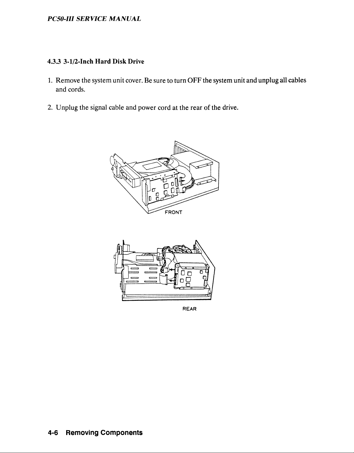
PC50-III SERVICE MANUAL
4.33 3-1/2-Inch Hard Disk Drive
1. Remove the system unit cover. Be sure to turn OFF the system unit and unplug all cables
and cords.
2. Unplug the signal cable and power cord at the rear of the drive.
4-6
Removing Components
Page 87
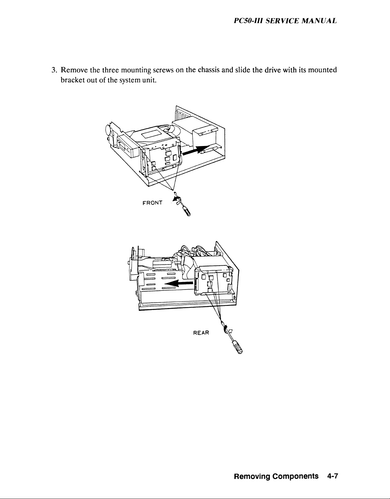
PC50-III SERVICE MANUAL
3. Remove the three mounting screws on the chassis and slide the drive with its mounted
bracket out of the system unit.
F R O N T
Removing Components
4-7
Page 88
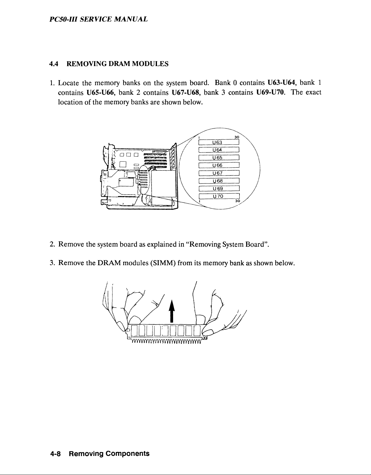
PC50-III SERVICE MANUAL
4.4 REMOVING DRAM MODULES
1. Locate the memory banks on the system board. Bank 0 contains U63-U64, bank 1
contains U65-U66, bank 2 contains U67-U68, bank 3 contains U69-U70. The exact
location of the memory banks are shown below.
2. Remove the system board as explained in “Removing System Board”.
3. Remove the DRAM modules (SIMM) from its memory bank as shown below.
4-8 Removing Components
Page 89
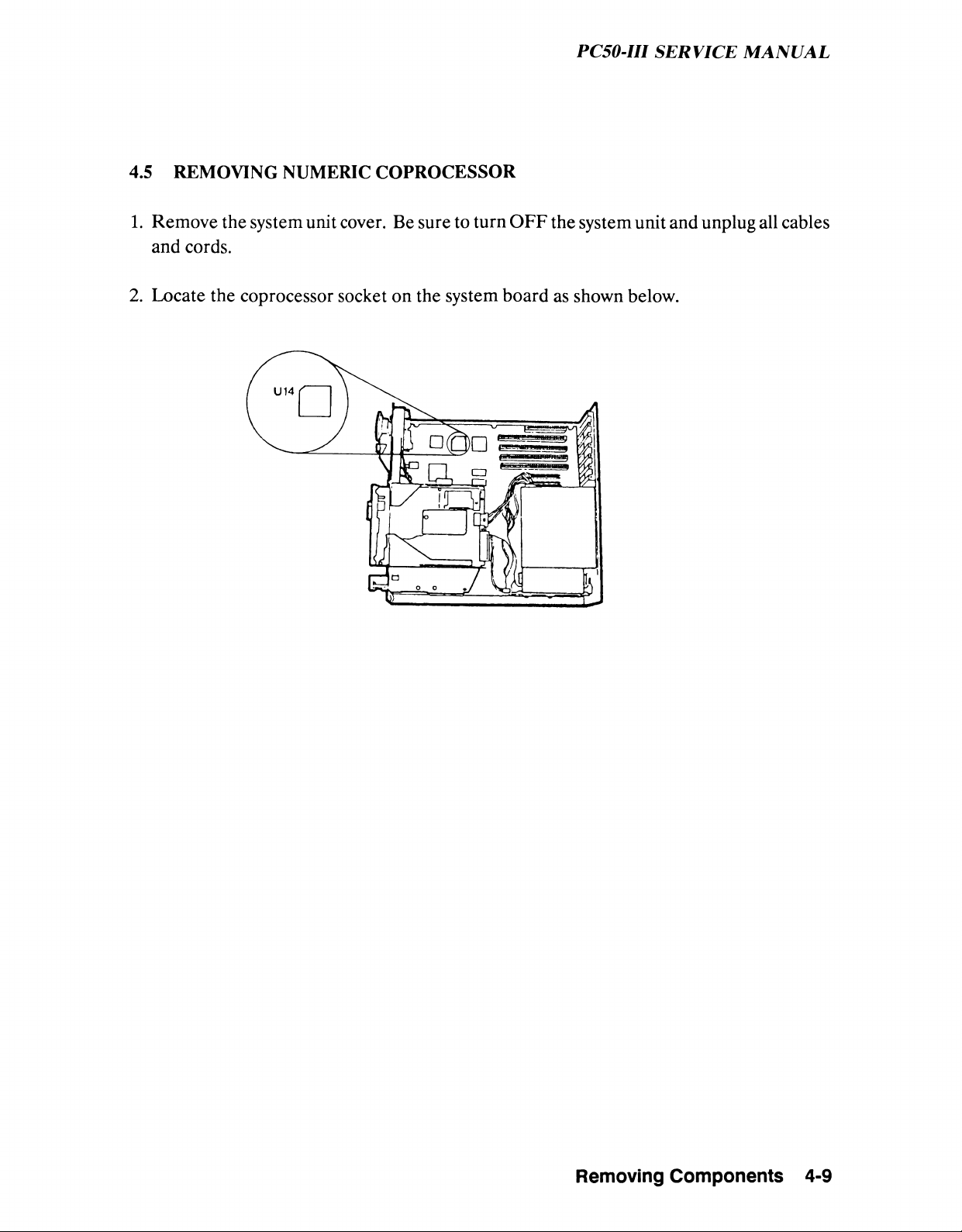
PC50-III SERVICE MANUAL
4.5 REMOVING NUMERIC COPROCESSOR
1. Remove the system unit cover. Be sure to turn OFF the system unit and unplug all cables
and cords.
2. Locate the coprocessor socket on the system board as shown below.
Removing Components
4-9
Page 90
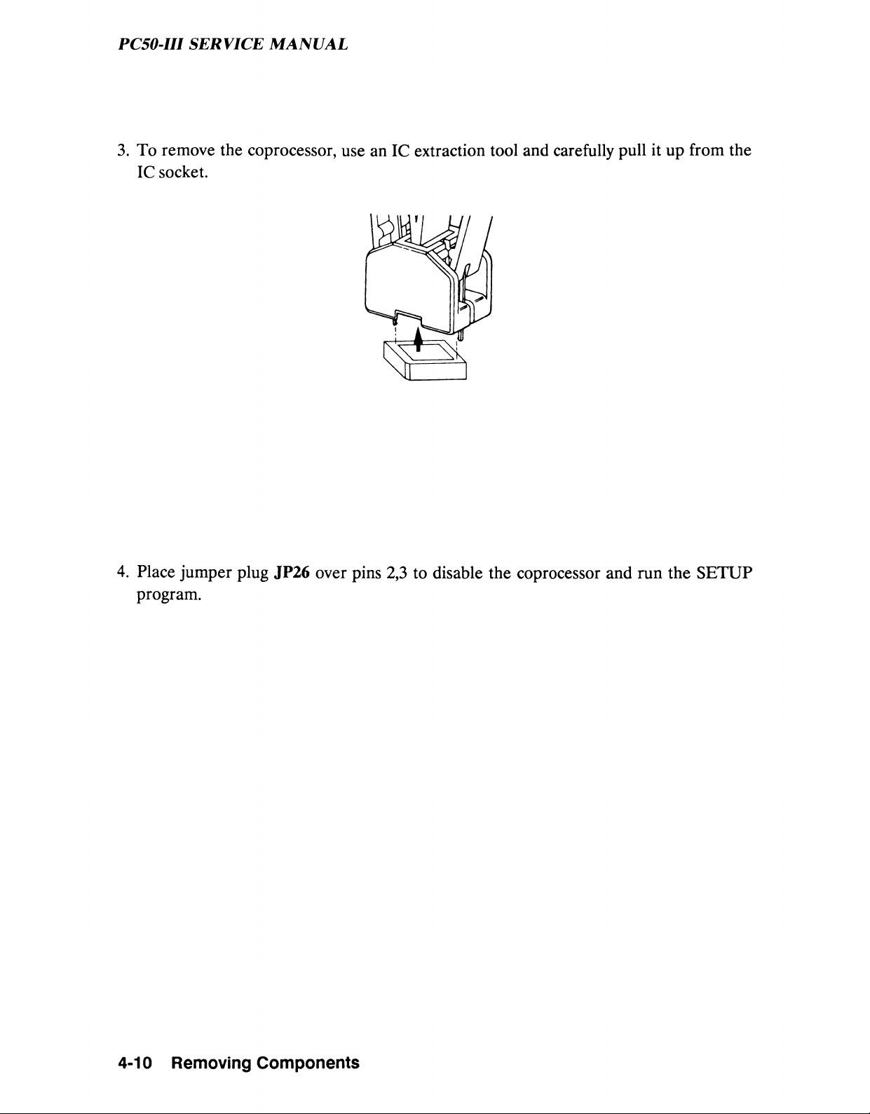
PC50-III SERVICE MANUAL
3. To remove the coprocessor, use an IC extraction tool and carefully pull it up from the
IC socket.
4. Place jumper plug JP26 over pins 2,3 to disable the coprocessor and run the SETUP
program.
4-10
Removing Components
Page 91
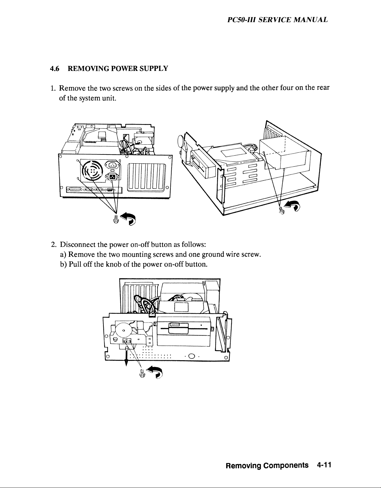
PC50-III SERVICE MANUAL
4.6 REMOVING POWER SUPPLY
1. Remove the two screws on the sides of the power supply and the other four on the rear
of the system unit.
2. Disconnect the power on-off button as follows:
a) Remove the two mounting screws and one ground wire screw.
b) Pull off the knob of the power on-off button.
Removing Components 4-11
Page 92
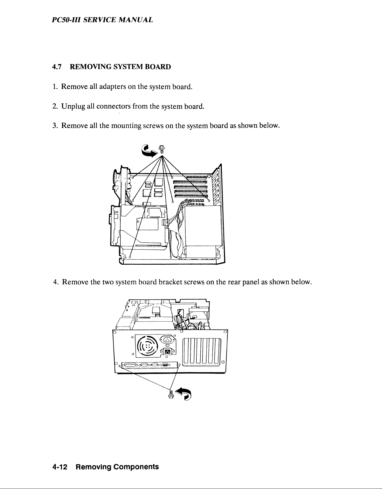
PC50-III SERVICE MANUAL
4.7 REMOVING SYSTEM BOARD
1. Remove all adapters on the system board.
2. Unplug all connectors from the system board.
3. Remove all the mounting screws on the system board as shown below.
4. Remove the two system board bracket screws on the rear panel as shown below.
4-12 Removing Components
Page 93
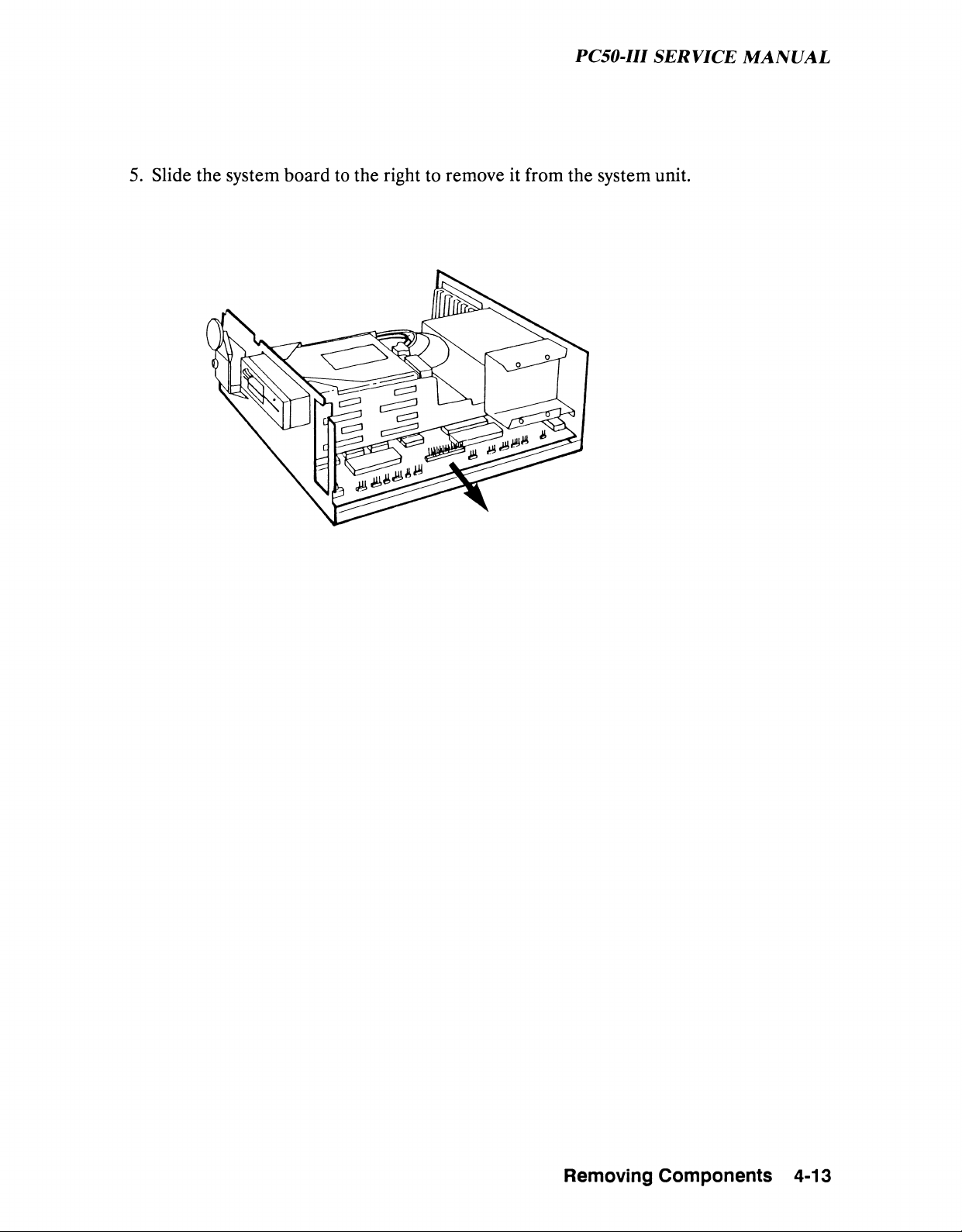
PC50-III SERVICE MANUAL
5. Slide the system board to the right to remove it from the system unit.
Removing Components 4-13
Page 94

Page 95
PC50-III SERVICE MANUAL
CHAPTER 5
DIAGNOSTICS
5.1 Diagnostics Program ................................................................................................. 5-1
5.1.1 System Checkout.........................................................................................................5-1
5.1.2 Shipping Preparation................................................................................................ 5-15
5.2 Power-On Self Test ................................................................................................. 5-15
5.2.1 POST Procedures.....................................................................................................5-16
5.2.2 POST Error Messages
..............................................................................................
5-17
Page 96

Page 97
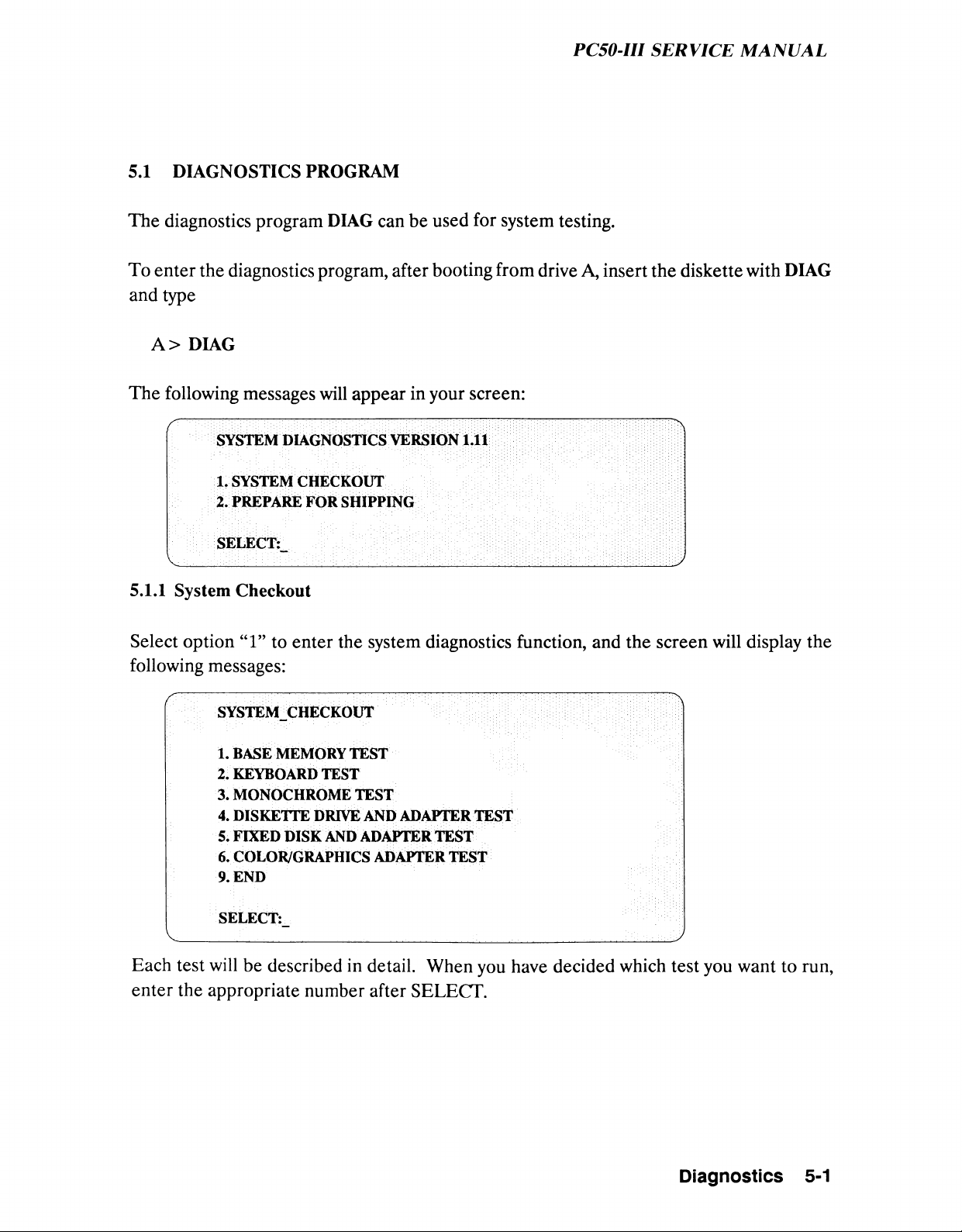
PC50-IU SERVICE MANUAL
5.1 DIAGNOSTICS PROGRAM
The diagnostics program DIAG can be used for system testing.
To enter the diagnostics program, after booting from drive A, insert the diskette with DIAG
and type
A> DIAG
The following messages will appear in your screen:
SYSTEM DIAGNOSTICS VERSION 1.11
1. SYSTEM CHECKOUT
2. PREPARE FOR SHIPPING
SELECT:_
5.1.1 System Checkout
Select option “1” to enter the system diagnostics function, and the screen will display the
following messages:
SYSTEM_CHECKOUT
1. BASE MEMORY TEST
2. KEYBOARD TEST
3. MONOCHROME TEST
4. DISKETTE DRIVE AND ADAPTER TEST
5. FIXED DISK AND ADAPTER TEST
6. COLOR/GRAPHICS ADAPTER TEST
9. END
SELECT:_
Each test will be described in detail. When you have decided which test you want to run,
enter the appropriate number after SELECT.
Diagnostics 5-1
Page 98
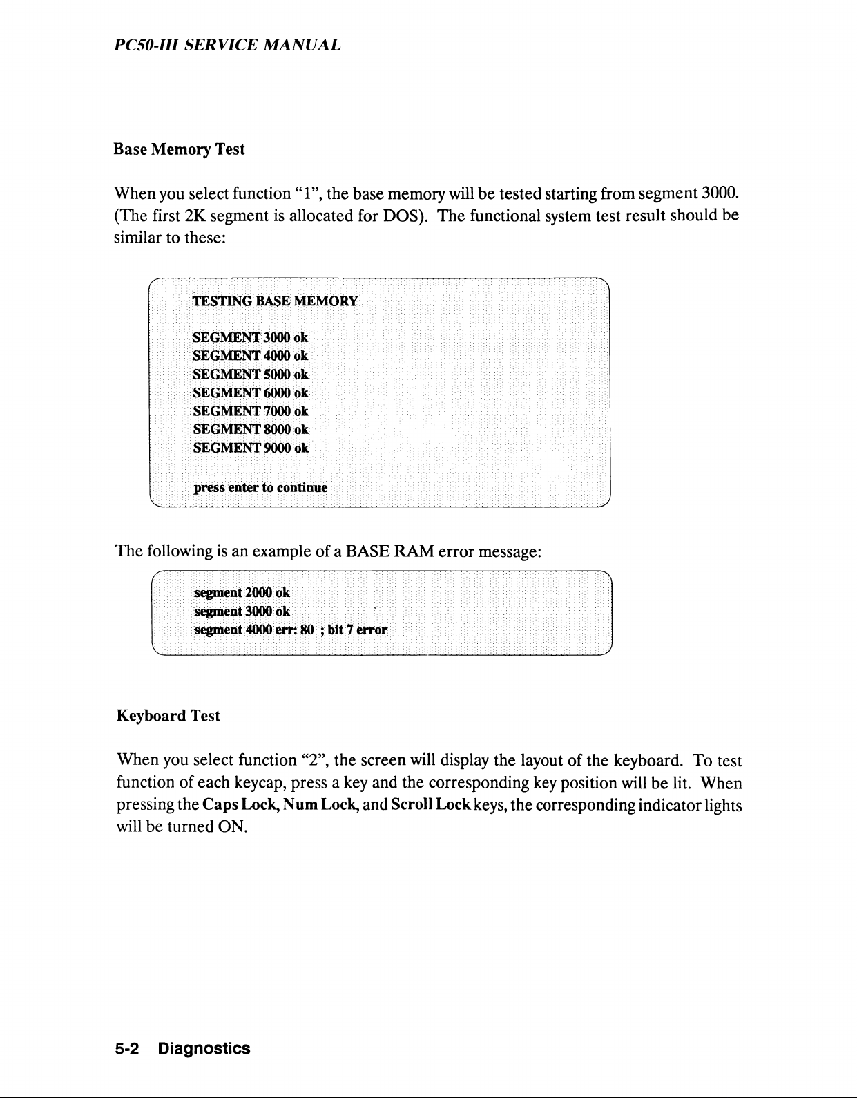
PC50-III SERVICE MANUAL
Base Memory Test
When you select function “1”, the base memory will be tested starting from segment 3000.
(The first 2K segment is allocated for DOS). The functional system test result should be
similar to these:
TESTING BASE MEMORY
SEGMENT 3000 ok
SEGMENT 4000 ok
SEGMENT 5000 ok
SEGMENT 6000 ok
SEGMENT 7000 ok
SEGMENT 8000 ok
SEGMENT 9000 ok
press enter to continue
The following is an example of a BASE RAM error message:
segment 2000 ok
:;:>v
segment 3000 ok
segmenit 4000 erh 80 ; bit 7 erroi
....
..............................
.....
,: i: i::: i i i; i i: i i i i i i i: i: i i::.::::
Keyboard Test
When you select function “2”, the screen will display the layout of the keyboard. To test
function of each keycap, press a key and the corresponding key position will be lit. When
pressing the Caps Lock, Num Lock, and Scroll Lock keys, the corresponding indicator lights
will be turned ON.
5-2 Diagnostics
Page 99
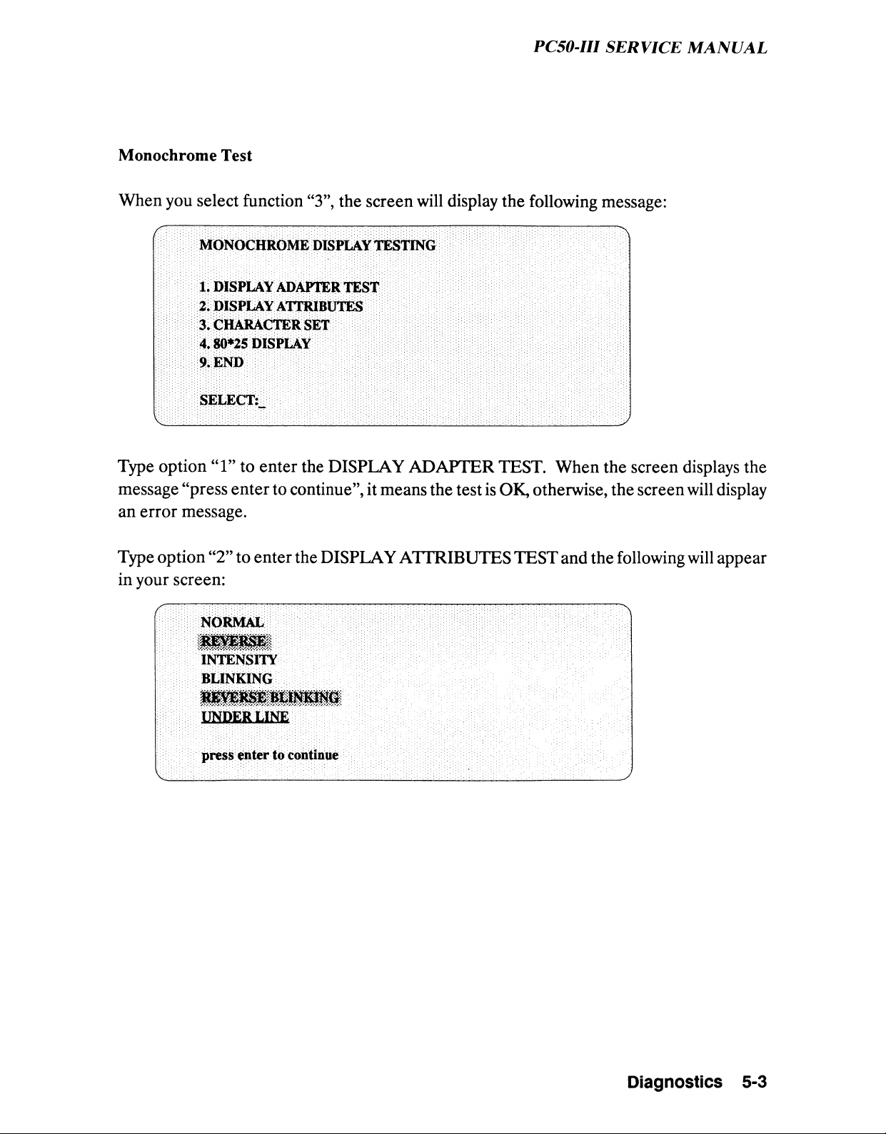
PC50-UI SERVICE MANUAL
Monochrome Test
When you select function “3”, the screen will display the following message:
MONOCHROME DISPLAY TESTING
...
1. DISPLAY ADAPTER TEST
4.80*25 Disp la y
.....
9. E N D
.
.........
.
......................
'M
Type option “1” to enter the DISPLAY ADAPTER TEST. When the screen displays the
message “press enter to continue”, it means the test is OK, otherwise, the screen will display
an error message.
Type option “2” to enter the DISPLAY ATTRIBUTES TEST and the following will appear
in your screen:
NORMAL
in t en sit y
blink in g
UNDERLINE
press enter to continue
Diagnostics 5-3
Page 100
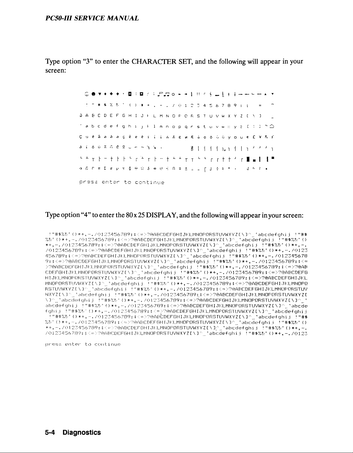
PC50-III SERVICE MANUAL
Type option “3” to enter the CHARACTER SET, and the following will appear in your
screen:
• ▼
"
•
•D A B C
a b c d e
6
^ i
L X
T
r n
a r>
7
HI
S f
'O
4
♦
S
*/.
n
D E F G H
a a A a
n M
u
l-t
z a
0 D t i
E?r
♦
■f
*
h
1'
□
•
(
h
q
ee£ l
5
0
-
L
Y
T
5
0
t
I
)
I
1
- -
r
H
c
□
t
J
J
X
*
o n
i p3
, -
*
\
L n N
i
1 m
i i
\ i
l -
r
t i n l i e
F=l
►
o
(j
/
*
p
Q
n
o
p q
A A
£ & ft o 0 6
X
X
t
=
n
-
1
0
T
+
\
11
7
2
R
STU
r
s
» 1 1
L L
T
- -
r
4
t Ll
r
i
-
1 1
r
j
L
\
—
6 7
8
W
V
X Yzc\]
V w
y
M
l
1.
t
t
r
0
6
1
9
y
o u
1
j
— —
1
r
<i
i
1
j
—
=
£
V
j . J j
1
■
f.
▼
▲
-
-
-
f
r,
1
■
1
■
Type option “4” to enter the 80 x 25 DISPLAY, and the following will appear in your screen:
1 ( ) *+ , / 0 1 2 3 4 5 6 78 ? : ; < y? i* A B C D E FG H IJK L MN O P QR S TU V W X YZ l \ 3y- r a b cd e-f g h i j !
VAA ( ) * + , /0 :1 . 23 4 5 6 7 8 9 ; ; < - >?i«!ABCBEFGH IJK LMN O P 0 R S T U V WX YZ l \ l y-
/ 0 1 23 4 56 7 8 9: 5 <==>?@ABCE>EFGHI JKLMN OP QR ST UV WX YZ l \ 3""._ ' a b cd ef q h i i f "#* 7. . V < > * + ,- .
/ 0 1 2 3 4 5 6 7 8 9 s ; < == >? 0AB CD E F'G H J. JKLM NG PQ RS TU VW X YZ f \ 3 - ... r a b c d t? f - qh i j ' " i t UY -V ( ) *+ , / 0 1 2 3
45 6 7 89 : ; • > ;■-70AB GDE FGH I JKLMNOPQR STl.JVWX YZ l \ 3 ""._ r a bcd e- f q h i j ! " # * ■ / .&” < ) / 0 12 34 56 78
9 ; ; < = >?@ A BC D E FG H I Jl CLNNuPQRSTUV WX YZ f \ 3"\._ r a b c d e f q h i j ! ( ) *•+•, /0 1 2 3 4 5 6 7 8 9 s ; < =
>?@ A B C DE F GH I JK U I N G F Q R S T U V WX V Z L \ 3'' r a b c d e f g h i j ! / 0 1 2 3 456 7 89: 5 < = >? @ A B
CDEFGI I IJ K L M N G P Q R S TU V WX V Z l \ 3 ‘ abcide f g h i i ! H #* " / . & ’ ( ) * + „ / 0 1 2 3 4 5 6 7 8 9 s 5 < = > ?@ A B C D E FG
H I JKLMNGF:,QRSTU VW XYZ l \ 3 r a b c d o f q h :i. j ! " #$"/.&■’ ( ) * + , - . /01234567 8 9 : ; < = >?@ABC DE FG H IJ K L
MNOPQR STUV WX YZ C \ 3 _ 11 ab c d e f g h i j ' " #*"/.& 9 ( ) *+ , / 0 1 2 345 6 7 89s 5 < = >?@ABC D EFG H IJ K L M NO PQ
RSTU VWX YZC \ 3" ... , abcd f? fq h i i ! "t t * 7.. V ( ) * + , -. / 0 1 2 34 5 678 9 : 5 < == /T H A B C D E F G H I JKL M N 0 P Q R S 3 T U V
WX YZ C \ 3 \_ r a b o d e f g h i j ! "tt* 7.S < ( ) •* + ,•- . /0 1 2 3 4 5 6 7 8 9 s,; < = >?@AE»CDEFGH I JKLM NO PQ R ST UV W X YZ C
\ 3 rab c de - f ; gh:L j ! ” IW /A r ( ) * + „ - . / 0 1 23 4 56 7 8 9: 5 < > >? @ AB C DE FG H I JKL M NG PQ RS TU V WX YZ [ \ 3 ‘ _. r
ab cde f g h i j ' " ’ ( ) * + , / 0 1 23 456 7 89: ; < == >?@ABC DE FGH IJKLMND PG3RS TUVWX YZ C \ 3 r abc de
f g h i. j ! " ®%VA.' ' ( ) * ->-, - „ / O I 2 345 6 7 89: r, < - > ? 0A B G D E F G H I JKLM N0PQ R8T I.JVW X YZ C \ 3 ' a b c d e f g h i j
1 / 0 1 2 3 456 7 8 9 s ; < = >?0 A B C D E FGH I J KLMNGPQRSTUV WX YZ C \ 3" "... r ab c d e f q h i .1 "l " # $
7.Zr ( ) * i- n /O 1 2 3 45 6 78 9 : ; >?i;aABCDEFGH 1JK LMM OPQ RST UVWX 'YZ l \ : b \ . r a b c d e f gh i ;i ! ( )
*■■+•,•-•■/0 1 2 345 6 78 9 : 5 •••; - > ?0 AB CDEF GM 1J l< L M1'^0PQRE3TLJVWX YZ l \ 3.. .. r a b c d e f g h i j 1 M #$7. Z3 ( ) * + , - .
/ 0 1 234 5 6 789 s ; < >?P A BC D E FG H I JKLMNdJF’QRSTUVWX YZ T \ 3 ' ■ _ r a b cde - f gh:L i ! "#$ 7Z 3 ( ) *+ , / 0 1 2 3
..
' a b c d e f g h i i 1 " # * 7.. V ( )
pre ss e nter to cnnti nue
5-4
Diagnostics
 Loading...