


Commodore® Amiga
®
A500/A2000
Technical Reference
Manual

COPYRIGHT
This manual is copyright © 1986,1987 by Commodore-Amiga, Inc. All Rights Reserved.
This document may not, in whole or part, be copied, photocopied, reproduced,
translated or transferred to any electronic medium or machine readable form
without prior consent, in writing, from Commodore-Amiga, Inc.
Amiga is a registered trademark of Commodore-Amiga, Inc.
Commodore and CBM are registered trademarks of Commodore Electronics Limited.
Hayes is a registered trademark of Hayes Microcomputer Products, Inc.
IBM is a registered trademark of International Business Machines Corporation,
Macintosh is a trademark of Apple Computer, Inc.
DISCLAIMER
THE INFORMATION IS PROVIDED "AS IS" WITHOUT WARRANTY OF ANY KIND, EITHER EXPRESSED
OR IMPLIED. THE ENTIRE RISK AS TO THE ACCURACY OF THE INFORMATION HEREIN IS
ASSUMED BY YOU. COMMODORE-AMIGA DOES NOT WARRANT, GUARANTEE. OR MAKE ANY
REPRESENTATIONS REGARDING THE USE OF. OR THE RESULTS OF THE USE OF, THE
INFORMATION IN TERMS OF CORRECTNESS, ACCURACY, RELIABILITY, CURRENTNESS. OR
OTHERWISE. IN NO EVENT WILL COMMODORE-AMIGA, INC. BE LIABLE FOR DIRECT, INDIRECT,
INCIDENTAL OR CONSEQUENTIAL DAMAGES RESULTING FROM ANY DEFECT IN THE
INFORMATION EVEN IF IT HAS BEEN ADVISED OF THE POSSIBILITY OF SUCH DAMAGES. SOME
LAWS DO NOT ALLOW THE EXCLUSION OR LIMITATION OF IMPLIED WARRANTIES OR LIABILITIES
FOR INCIDENTAL OR CONSEQUENTIAL DAMAGES. SO THE ABOVE LIMITATION OR EXCLUSION MAY
NOT APPLY.
Schematics represent current machine which is subject to change without notice.
Credits
The material for this manual was produced by Engineering. Documentation,
and Technical Support staff at Commodore West Chester, Commodore
Braunschweig, and Commodore-Amiga. Individuals contributing major portions of information and input are Dave Haynie, Jeff Porter, Phil Lindsay,
Carolyn Scheppner, Lisa Siracusa. George Robbins. Andy Finkel. Eric
Cotton, Jeff Boyer, Steve Ahlbom, Steve Beats, Dieter Preiss, Bernd
Assmann, and Torsten Burgdorf.
This manual was compiled and edited by Steve Finkel.
Manual design by Jo-Ellen Temple and Wilson Harp.

A2000/A500 Technical Reference Manual
Table of Contents
Section 1
Summary of Differences
1
Section 2 System Block Diagrams
13
Section 3
Amiga Expansion
3.1
Designing hardware for the Amiga Expansion
Architecture
17
3.2
Driver Documentation
51
3.3 Software for Amiga Expansion
55
3.4
Amiga Expansion Connectors
100 Pin
75
86 Pin
87
Video Slot
101
Section 4
PC Bridgeboard
4.1
Description of the PC/XT emulator for the Amiga 2000
109
4.2
BIOS entry points
121
4.3 Janus library
131
Section 5
Amiga Hard Disk/SCSI Controller
159
Section 6
Custom Chips
Fat Agnus Chip
187
8520 Chip
213
Section 7
Miscellaneous Hardware Information
223
7.1
Clock/calendar registers
225
7.2 Power budgets
229
7.3
A2000 PAL equations
235
7.4
B2000 Jumpers
Appendix A.
Diagrams
A-1
Backplane Example
A-1
A-2
PIC Example
A-2
A-3
A500 Exterior (86-pin expansion connector)
A-3
A-4
Amiga 2000 Expansion Board Layout
A-4
A-5 Amiga 2000 Form Factor
A-5
A-6
Amiga 2000 Video Card
A-6
A-7
86-Pin Slot Expansion Board
A-7
A-8
A2000/B2000 Keyboard Connector Pinout
A-8
A-9
Amiga 500/2000 Mouse Diagram and Pinout
A-9
Appendix B.
Schematics
A2000 Schematics
A2000-1
B2000 Schematics
B2000-1
A500 Schematics
A500-1

Section 1
Summary of Differences
KICKSTART IN ROM
This manual presents technical documentation for three different
Amiga models, comparing them to the original Amiga, referred to as
model A1000. Technical information included in this manual is relevant for the following Commodore Amiga models:
● the Amiga 500 (A500), a low-cost version of the origi-
nal Amiga computer, software-compatible with the
A1000. Unlike the A1000, the A500 has an integrated
keyboard, provision for internal memory expansion up
to 1 megabyte, new-style hardware connectors, and
Kickstart code in ROM.
Two versions of the Amiga 2000:
● the A2000 is software-compatible with the A1000 and
has internal slots, real time clock/calendar and newstyle hardware connectors.
● the B2000, the cost-reduced version of the Amiga
2000, features some different custom chips, but is
otherwise similar to the A2000.
The B2000 is still under development, and the information presented in this document is subject to change. The information included
on the B2000 is intended to aid developers in designing software
and peripherals that are applicable for both the current and
upcoming version of the Amiga 2000.
Unless differences are specifically noted, information presented for
the A2000 also holds true for the B2000. The differences between
the two Amiga 2000 models are mainly hardware differences which
will affect peripheral design, but not the way the computers function
with software. Section 2 contains system block diagrams for all
three new Amiga models.
Both the Amiga 2000 and the Amiga 500 feature version 1.2 of
Kickstart built into ROM. Kickstart 1.2 (currently version 33.180)
boots automatically when the Amiga is turned on.
1
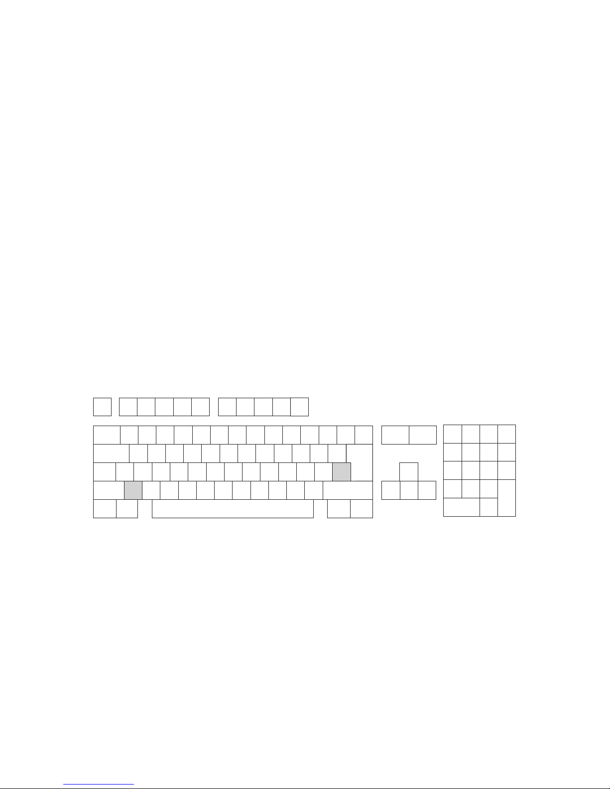
EXTRA KEYS ON THE
KEYBOARD
RAW KEY CODES ON
THE KEYBOARD
Both the Amiga 2000 and 500 feature 94-key keyboards, as compared to the A1000's 89-key keyboard. (The European versions of
the keyboards have 96 keys.) The new keys are all located on the
numeric keypad, and include:
KEY SCAN CODE
Left parentheses ( $5A
Right parentheses ) $5B
Slash / $5C
Asterisk * $5D
Plus + $5E
In PC mode on the Amiga 2000 (using a Bridgeboard), these keys
assume typical PC functions, including Number lock (left parenthesis), Print screen (asterisk) and Scroll lock (right parenthesis).
On some keyboards, the left Amiga key has been replaced by the
Commodore key. This key performs identically in either case.
Keyboard Layout Showing Raw Key Codes
45 50 51 52 53 54 55 56 57 58 59
3F
4A
3D 3E
14 15 16 17 18 19 1A 1B42 10 11 12 13
0D 41 46 5F
5B 5C 5D
5A
05 06 07 08 09 0A 0B 0C00 01 02 03 04
67 654064 66
1F
43
1D 1E
2E 2F 5E
2A
0F 3C
4C63 28 29 2A 2B
44
20 21 22 23 24 25 26 2762
3A 61 4F 4D 4E33 34 35 36 37 38 3960 30 31 32
Figure 1.1 Key Codes
Note: On the U.S. keyboard, the keys with codes 44 and 60 are
extended to include the European keys with codes 2B and 30,
respectively. Also note that England uses the U.S. rather than
the European keyboard, but not the U.S. keymap.
See Table 1-1 at the end of this section for a table of the raw key
codes.
2

EXTERNAL SYSTEM I/O
RS232 and MIDI Port
12345678910111213
141516171819202122232425
This section describes each I/O interface in detail, and some of the
tradeoffs made with respect to A1000 compatibility.
The Amiga 2000 and Amiga 500 have differences in the serial and
parallel ports from the Amiga 1000, the main difference being
changes in the sex of each port (changing the serial to female and
the parallel to male), which allows the new Amigas to use standard
interface cables.
The RS232 connector on the A500 and A2000 is form fit and
function identical to a Commodore PC-10/20 with a few
exceptions. This is the OPPOSITE sex connector from the
A1000. The connector is a shielded male DB25P connector. The
A1000 supplies various non-standard RS232 signals on the DB25
connector. These non-standard signals were removed wherever
possible. The RS232 connector is NOT physically compatible with
some MIDI interfaces but is compatible with the Amiga
Modem/1200 RS {model 1680). Below is a comparison chart
between the RS232 standard, a Hayes Smart-modem standard, the
A1000 RS232, and the new Amiga 500/2000 RS232 connector.
PIN RS232 A1000
A500/
A2000 PC10 HAYES® DESCRIPTION
1 GND GND GND GND GND Frame
g
round
2 TxD TxD TxD TxD TxD Transmit Data
3 RxD RxD RxD RxD RxD Receive Data
4 RTS RTS RTS RTS
—Req
uest to send
5 CTS CTS CTS CTS CTS Clear to send
6 DSR DSR DSR DSR DSR Data set read
y
7 GND GND GND GND GND Signal ground
8 DCD DCD DCD DCD DCD Carrier detec
t
9—
—
+ 12v + 12v
—
+ 12 volt power
10 —
—
- 12v - 12v
—
- 12 volt power
11 —
—
A
UDO
——A
udio outpu
t
12 S.SD
———
SI Speed Indicate
13 S.CTS
———
—
14 S.TxD -5Vdc
—
—
—
- 5 volt power
15 TxC
A
UDO
—
——A
udio outpu
t
16 S.RxD
A
UDI
—
——A
udio inpu
t
17 RxC EB
—
—
—
Port clock 716KHz
18 — INT2*
A
UDI
—
—
Interrupt line/Audio inpu
t
19
S.RTS
———
—
20 DTR DTR DTR DTR DTR Data terminal read
y
21 SQD+ 5Vdc—
—
—
+ 5 volt power
22 RI
—
RI RI RI Ring indicator
23 SS + 12Vdc —
—
—
+ 12 volt power
24 TxC1 C2*
—
—
—
3.58MHz clock
25 — RESB*
—
—
—
Buffered system
3

Centronics Port
1234
5678910
11 12
13
14
15 161718 19 20
21 222324
25
Video Output
As you will notice, the A500 and 2000 deletes clocks and interrupt
lines from the A1000. The +/-5Vdc and reset lines are also deleted.
The +/- 12Vdc lines are identical to a PC10/20.
The following signals (formerly on the RS232 connector) can be
found on other connectors:
ResB = parallel connector
C2 = video connector
The Centronics port also has some non-standard signals. Below is a
table comparing the A1000 Centronics port with the A500/A2000
Centronics port. Again, this is the opposite sex from the A1000
and the same sex connector as an IBM®-PC (i.e., a female DB25
connector).
PIN A1000 A500/A2000 PC10
1 DRDY* STROBE* STROBE*
2 Data O Data O Data O
3 Data 1 Data 1 Data 1
4 Data 2 Data 2 Data 2
5 Data 3 Data 3 Data 3
6 Data 4 Data 4 Data 4
7 Data 5 Data 5 Data 5
8 Data 6 Data 6 Data 6
9 Data 7 Data 7 Data 7
10
A
CK*
A
CK*
A
CK*
11 BUSY
(
data
)
BUS
Y
BUS
Y
12 POUT(clk
)
POUT POUT
13 SEL SEL SEL
14 GND + 5v
p
ullu
p
A
UTOFDXT*
15 GND NC ERROR*
16 GND RESET* INIT*
17 GND GND SLCT IN*
18-22 GND GND GND
23 + 5v GND GND
24 NC GND GND
25 Reset* GND GND
The A500 and A2000, like the A1000, use a DB23 video connector.
This 23 pin connector contains all the signals necessary to work with
a Genlock, but the current Genlock will need to be redesigned in order to meet the physical requirements of the A500 and A2000, in
4

Mouse and Joystick
Ports
A500 Expansion Port
A500 RAM Expansion
A500 Power Supply
Connector
stead of the A1000. An A500 genlock will also have to supply its
own power. Power will not be provided for the Genlock. All signals
on the 23 pin connector are the same except for the power.
In addition to the 23 pin video connector, the A500/B2000 provides
a monochrome composite video output, unlike the A1000. This provides the capability of using a low-cost, high persistence monochrome monitor with the A500 for viewing 640 x 400 interlaced
video without as much flickering.
Power is provided for the A520 modulator and composite video
adapter.
The mouse and joystick ports of the A500 and A2000 are identical
to the A1000, except that the current limiting protection circuitry
has been eliminated. The A500 and A2000 use a different mouse
than the one the A1000 uses. A diagram and information on this
mouse is included in Appendix A of this manual.
The expansion port is electrically compatible with the A1000, but
because of its physical location, it cannot accept any A1000
expansion peripherals without some further adapter. Power is
supplied to this connector, but only enough for a ROM cartridge.
The exact pinout of this 86 pin edge connector appears later in this
document,in the section of Amiga expansion. The A500 diagram in
Appendix A shows the new positioning of this port (relative to
A1000) and the pin numbers.
Associated with the built-in 512KB of RAM is a header socket to allow an additional 512KB of RAM and a battery backed-up real time
clock board to be added. This small PCB (the A501 RAM Expansion
Cartridge) can easily be installed by the user. The clock in this unit
functions the same as that built into the A2000, which is reviewed
in Section 7-1.
The A500 power supply connector is similar to that of the C128.
The pinout of the square 5 pin DIN connector is as follows:
PIN SIGNAL
1 + 5Vdc @ 4.3A
2 Shield Ground
3 + 12Vdc@ 1.0A
4 Signal Ground
5 -12Vdc @ .1A
5

External Disk Interface
Connector
The 23 pin D-type connector with sockets (DB23S) at the rear of the
Amiga is nominally used to interface to MFM devices.
The second disk drive port is similar to the A1000, and is therefore
compatible with the 1010 or the 1020 disk drive. The CPU will
power one external 1010 disk drive.
External Disk Connector Pin Assignment
Pin Name Dir Notes
1 RDY* I/O If motor on, indicates disk
installed and up to speed.
If motor not on, Identification
mode. See below.
2 DKRD* I MFM input data to Amiga.
3GND
4GND
5GND
6GND
7GND
8 MTRXD* OC Motor on data, clocked into
drive's motor on flip flops by the
active transistion of SELxB*.
Guaranteed setup time is 1.4
μsec
Guaranteed hold time is 1.4
μsec.
9 SEL2B*/SEL3B*0C A500:Select drive 2/A2000:
Select drive 3.
10 DRESB* OC Amiga system reset. Drives
should reset their motor on flip
flops and set their write protect
flip flops.
11 CHNG* I/0 Note: Nominally used as an open
collector input. Drive's change
flop is set at power-up or when
no disk is installed. Flop is reset
when drive is selected and the
head stepped, but only if a disk is
installed.
12 5V 270 ma maximum; 410 ma
surge.
When below 3.75V, drives are
required to reset their motor on
flops, and set their write protect
on flops.
13 SIDEB* 0 Side 1 if active, side 0 if inactive.
14 WPR0* I/O Asserted by selected, write
protected disk.
6

15 TKO* I/0 Asserted by selected drive
when read/write head is
positioned over track 0.
16 DKWEB* OC Write gate (enable) to drive.
17 DKWDB* OC MFM output data from
Amiga.
18 STEPB* OC Selected drive steps one
cylinder in the direction
indicated by DIRB.
19 DIRB OC Direction to step the head.
Inactive to step towards
center of disk (higher
numbered tracks).
20 SEL3B*/
Not Used
OC A500: Select drive 3/A2000:
Not used.
21 SEL1B/SEL2B OC A500: Select drive 1/A2000:
Select drive 2.
22 INDEX* I/O Index is pulse generated once
per disk revolution, between
the end and beginning of
cylinders. The 8520 can be
programmed to conditionally
generate a level 6 interrupt to
the 68000 whenever the
INDEX* input goes active.
23 + 12V 160 ma maximum; 540 ma
surge.
Note: * in signal name denotes active low signal.
External Disk Connector Identification Mode
An identification mode is provided for reading a 32 bit serial identification data stream from an external device. To initialize this mode,
the motor must be turned on then off. See pin 8, MTRXD* for a
discussion of how to turn the motor on and off. The transition from
motor on to motor off reinitializes the serial shift register.
After initialization, the SELxB* signal should be left in the inactive
state.
Now enter a loop where SELxB* is driven active, read serial input
data on RDY* (pin 1), and drive SELxB* inactive. Repeat this loop a
total of 32 times to read in 32 bits of data. The most significant bit
is received first.
7

Full Bus Termination
Internal RAM
Expansion on the A500
EIA Ring Indicate
Support
External Disk Connector Defined Identifications
$0000 0000 - no drive present
$FFFF FFFF - Amiga standard 3.25 diskette
$5555 5555 - 48 TPI double density double sided
As with other peripheral ID's, users should contact Commodore Technical Support for ID
Assignment.
The serial input data is active low and must therefore be inverted to be consistent with the above
table.
External Disk Connector Limitations
1. The total cable length including daisy chaining
must not exceed 1 meter.
2. A maximum of 3 external devices may reside
on this interface (2 for the A2000).
3. Each device must provide a 1000 Ohm pullup
resistor on every open collector input.
Unlike the A1000 and the A500, both versions of the Amiga 2000
have an internal expansion bus, as a function of having an internal
card cage.
On the A500, memory at $C00000 is "slow" RAM (the processor is
locked out by the custom chips) rather than fast RAM as suggested
by A1000 external expansion. Thus, when ExecBase is transferred
to $C00000 to free up chip RAM, there is no speed advantage.
However, you would still be making real chip RAM available for
other purposes. The B2000 functions as the A500 does in this
regard.
The A500. A2000 and B2000 support the RS232 RI lead to allow
operation with modem standards. When the RI signal is asserted,
the parallel port SEL line will be driven low. If this function is not
desired, the RI lead should be disconnected in the modem cable.
8

Time of Day Clock
Light Pen
Monochrome
Composite Video
Audio Filter Cut-out
A500 Reset
A2000 Expansion Bus
IPL Lines
In the A500. the Time of Day clock is tied to the VSYNC signal
rather than the power line. This results in the theoretical error of
several minutes a day. For more precise timing, use the optional
real-time clock.
In genlock mode, the genlock peripheral provides a 30 Hz V/Z
signal, which results in the clock running half speed.
The light pen input on the A500 and B2000 has been moved to the
second mouse port to allow use without a pass-thru mouse adapter.
On a B2000. the light pen can be jumpered to port 0.
The A500 and B2000 provide a full-bandwidth 16-level grey-scale
composite video output. Color composite is available with an
optional A520 composite color/rf video adapter.
The A500 and B2000 can cut out the anti-aliasing filter by programmatically turning off the "power on" LED. External bandwidth limiting to below 15 KHz will be required for most applications. This
permits wider frequency response by using faster sampling rates.
The A500 implements a "hard-wired" Control/Commodore/Amiga
key reset rather than the "soft" A1000/A2000 keyboard reset.
"Shut down" keyboard messages are not transmitted.
The A2000 does not run the processor IPL lines beyond the 86 pin
MMU connector. Instead, additional interrupt request lines are allocated for future expansion devices. These lines are not supported by
the current software.
9

Table 1 -1 RAW KEY CODES
Raw Key
Number Keycap Legend
Unshifted
Default
Value
Shifted
Default
Value
00 ‘ ~ ' (Accent grave) ~ (tilde)
01 1 ! 1 !
02 2 @ 2 @
03 3 # 3 #
04 4 $ 4 $
05 5 % 5 %
06 6 ^ 6 ^
07 7& 7 &
08 8* 8 *
09 9 ( 9 (
OA 0 ) 0 )
OB - _ - (Hyphen) _ (Underscore)
OC = + = +
OD \ │ \ │
OE (undefined)
OF 0 0 0 (Numeric pad)
10 Q q Q
11 W w W
12 E e E
13 R r R
14 T t T
15 Y y Y
16 U u U
17 I i I
18 O o O
19 P p P
1A [ { [ {
1B ] } ] }
1C (undefined)
1D 1 1 1 (Numeric pad)
1E 2 2 2 (Numeric pad)
1F 3 3 3 (Numeric pad)
20 A a A
21 S s S
22 D d D
23 F f F
24 G g G
25 H h H
26 J j J
27 K k K
28 L 1 L
29 ; :
2A ‘ ” ' (single quote) "
10

Raw
Key
Number
Keycap
Legend
Unshifted
Default
Value
Shifted
Default
Value
2B (RESERVED) (RESERVED)
2C (undefined)
2D 4 4 4 (Numeric pad)
2E 5 5 5 (Numeric pad)
2F 6 6 6 (Numeric pad)
30 (RESERVED) (RESERVED)
31 Z z Z
32 X X X
33 C c C
34 V V V
35 B b B
36 N n N
37 M m M
38 , < , (comma) <
39 . > . (period) >
3A /? / ?
3B (undefined)
3C . (Numeric pad)
3D 7 7 7 (Numeric pad)
3E 8 8 8 (Numeric pad)
3F 9 9 9 (Numeric pad)
40 (Space bar) 20 20
41 BACK SPACE 08 08
42 TAB 09 09
43 ENTER OD OD (Numeric pad)
44 RETURN OD OD
45 ESC 1B 1B
46 DEL 7F 7F
47 (undefined)
48 (undefined)
49 (undefined)
4A - - - (Numeric Pad)
4B (undefined)
4C Up Arrow <CSI>A <CS!>T
4D Down Arrow <CSI>B <CSI>S
4E Forward Arrow <CSI>C <CSI> A
1
4F Backward Arrow <CS1>D <CSI> @
1
In shifted Forward Arrow and Backward Arrow, note blank space after <CSI>.
<CSI> stands for Command Sequence Initiator.
11

Raw
Key
Number
Keycap
Legend
Unshifted
Default
Value
Shifted
Default
Value
50 F1 <CSI>0~ <CSI>10~
51 F2 <CSI>1~ <CSI>11~
52 F3 <CSI>2~ <CSI>12~
53 F4 <CSI>3~ <CSI>13~
54 F5 <CSI>4~ <CSI>14~
55 F6 <CSI>5~ <CSI>15~
56 F7 <CSI>6~ <CSI>16~
57 F8 <CSI>7~ <CSI>17~
58 F9 <CSI>8~ <CSI>18~
59 F10 <CSI>9~ <CSI>19~
5A ( ( (
5B ) ) )
5C / / /
5D * * *
5E + + +
5F HELP <CSI>?~ <CSI>?~
12

Section 2
System Block Diagrams
INTRODUCTION
This section features system block diagrams for each new Amiga,
the A2000, B2000 and A500, in that order.
13

62 pin PC - Connector
PA U L A
62 pin PC - Connector
PC
PRINTER FLO PPY
ext. int.
RS 232
AUDIO
MOUSE
JO Y -ST IC K
VIDEO
- RG B
BATTERY
REAL
TIM E
CLOCK
PARALLEL
PO R T
FLO PPY
PO R T
SERIAL INTERFACE
MOUSE INTERFACE
JOY - STICK INTERFACE
STEREO AUDIO INTERFACE
WITH 4 D/A CONVERTER
AT
36 pin Conn.
36 pin Conn.
AD
AC
AA
AD
AC
AA
100 pin AMIGA - Connector
100 pin AMIGA - Connector
D
DATA
BU FFE R
CONTROL
BU FFE R
ADDRESS
BU FFE R
C
A
86 pin MMU - Connector
D
D
C
C
A
A
A
A
A
D
D
D
D
D
C P U
6 8 0 0 0
A<1:23>
DATA
BU FFE R
ADDRESS
BU FFE R
ADDRESS
MUX
KICK
STA R T
ROM
ADDRESS
MUX
BLITTER
AGNUS
BIT D M A
CO NTRO LLER
GRAPHIC
CO NTRO LLER
512K 8 BIT∗
CHIP - RAM
DRAM
A M I G A
2 0 0 0
IA
ID
ID<0:15>
ID
IA
IA<1:8>
IA
ID
IA
ID
ID
D E N I S E
VIDEO CONTROLLER
VIDEO MOD.
14
62 pin PC - Connector
PA U L A
PC
PRIN TER
FLO PPY CO NTROL
RS 232
DATA
AUDIO
PO TS
CO M PO SITE/
M ONOCHROM E
VIDEO
- RG B
BATTERY
REAL
TIM E
CLOCK
PARALLEL
PO R T
FLO PPY
PO R T
SERIAL INTERFACE
MOUSE INTERFACE
JOY - STICK INTERFACE
STEREO AUDIO INTERFACE
WITH 4 D/A CONVERTER
AT
36 pin Conn.
AD
AC
AA
AD
AC
AA
100 pin AMIGA - Connector
100 pin AMIGA - Connector
D
DATA
BU FFE R
CONTROL
BU FFE R
ADDRESS
BU FFE R
C
A
86 pin MMU - Connector
D
D
C
C
A
A
A
D
D
D
D
D
C P U
68000
A<1:23>
DATA
BU FFE R
KICK
STA R T
ROM
BLITTER
FAT
AGNUS
BIT DMA
CONTROLLER
GRAPHIC
CONTROLLER
CHIP RAM
512K 8 BIT∗
DRAM
B 2000
ID
ID<0:15>
ID
IA
IA<1:8>
IA
ID
IA
ID
D E N I S E
VIDEO CONTROLLER
VIDEO MOD.
62 pin PC - Connector
36 pin Conn.
BUS CONTROL
&
ARBITRATION
BUSTER
BUFFER
CONTROL
KEYBOARD
RS 232
CONTROL
FLO PPY
DATA
MOUSE
Video
Hybrid
Video 1
36
PIN
36
PIN
Video 2
RA
ID
NONCHIP RAM
512K 8 BIT∗
DRAM
15

68000
CPU
AS
R/W
DTACK
Clocks
GARY
Full 68000
Bus
REAL
TIME
CLO CK
EXPANSION POR T
(Up to 8M Bytes)
28 Mhz
Clock
8520 CHIPS (2)
KEYBOARD
AS
R/W
Clocks
Control
DBR
FAT
AGNUS
Address Bus
Bi Directional
Tri State Latch
ROM
Data Bus
(16)
DRAM
512K Std.
1MB optional
Data Bus (16)
Multiplexed
Addresses
(9)
RAS0 1
CAS0 1
R/W
DMA Request
(DMAL)
DENISE
PAULA
RGA Register Address (8)
Printer Port
Disk Control
RS232 Control
VIDEO HYBRI
D
Mouse
Ports (2)
Video
RGB
Composite
Video
Disk
UART
Audio
Pot Port
A 500 BLOCK DIAGRAM
16

Section 3.1
Designing Hardware for the Amiga Expansion
Architecture
INTRODUCTION
This section gives guidelines for designing hardware to reside on the
Amiga expansion bus. The Amiga expansion bus is a relatively
straightforward extension of the 68000 bus.
Hardware for the bus can be viewed as two categories: backplanes
and PICs. Backplanes interface to the 86 pin connector of either
another backplane or the Amiga itself. Backplanes buffer the bus
and provide 100 pin connectors for PICs to plug into.
PIC is an acronym for plug-in card. A PIC is usually a card that plugs
into the standard 100 pin Amiga connectors.
A sub-type of PIC is a combination of backplane and PIC integrated
into one package. These combination products should follow all of
the applicable backplane and PIC rules, especially auto-configuration.
Software never sees backplanes; all expansion hardware appears to
the software as PICs.
WARNING
These specifications represent "worst case" design targets.
Products that do not comply with these specifications can be expected to fail on worst case production units.
Following conservative design practices and allowing the widest
safety margins is your best assurance against problems in the
field.
17
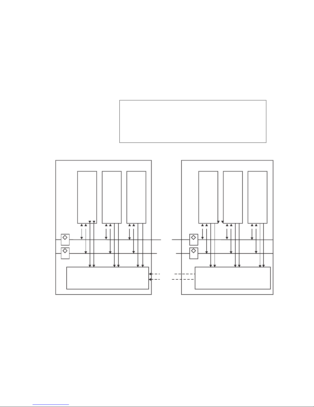
EXPANSION
ARCHITECTURE
OVERVIEW
As shown in Figure 3.1, "Expansion Architecture Overview," the expansion bus is implemented as backplane (an expansion box) which
accept PICs (boards). The recommended number of PICs to a backplane is five.
Due to timing considerations, it is not possible to daisy-chain more
than two buffered backplanes without inserting wait states.
NOTE
You should also take extreme care in controlling signal
radiation from your product, in order to pass FCC class B
regulations.
DOWNSTREAM BACKPLANE
PIC PIC PIC
S
L
A
V
E
O
W
N
B
U
F
F
E
R
S
A
M
I
G
A
COLLISION
BUS STEERING and ENABLE
BUS ARBITRATION
UPSTREAM BACKPLANE
PIC
PIC
PIC
DATA
COLLISION
BUS STEERING and ENABLE
BUS ARBITRATION
ADDRESS
SLAVE*
DMA*
Figure 3.1. Expansion Architecture Overview
18

GLOSSARY
Active Active high signals are considered active when they are in
the "one state" or "high state". Active low signals are considered active when they are "low" or in the “zero state”. Active high signals
do not have barred signal names. Active low signals do have barred
signal names. Active means that the signal is
1. is true (non-barred) and is currently in the one state, or
2. is a barred signal name and is currently in the zero state.
An example is AS* (the * = bar). AS* is active when it is equal to
zero. A counter example is the signal AS (the inverse of AS*), which
is active when it is in the one state.
Auto Configuration The protocol (specified in this section) that
Amiga uses to configure expansion cards into the system.
Downstream Downstream means closer to the Amiga. For instance, if two backplanes are daisy chained on the bus, the closer-in
backplane is downstream from the further-out backplane. The concepts of upstream and downstream are important in determining
which direction the address and data drivers should drive.
Master A PIC which is capable of initiating DMA cycles on the bus.
PIC A PIC is a plug-in card or a product which behaves in the system
as a plug-in card. That is, it provides a resource that resides on the
expansion bus, and follows the rules for auto-config, master protocol, slave protocol, etc.
Slave A slave is a PIC that can only respond to bus cycles. A slave
cannot initiate bus cycles: in other words, it does not drive the address lines on the backplane, nor AS*, UDS*, LDS*.
Upstream Upstream means further away from the processor. For
instance, all PICs are upstream from the buffers on the backplane
that they are plugged into because the buffers are between the PIC
and the Amiga.
19

DESIGN GUIDELINES
FOR BACKPLANES
Collision Detection
Circuit
Bus Arbitration Logic
In this context, collisions are defined as any instance of two slaves
attempting to respond to the same bus cycle.
All backplanes must have a collision detect circuit. The reason is that
the PICs are auto-configurable and can be accidently instructed by
software to respond to overlapping address spaces. Without collision
detection, erroneous software can damage the hardware by causing
bus contention.
Collision detect works in the following way: As soon as a PIC knows
that it has been selected as the slave for this bus cycle, it asserts
SLAVE* low and holds SLAVE* low until the end of the bus cycle
(AS* going high).
The collision detect circuit (usually part of a PAL) detects whether
more than one slave is responding and, if so, asserts BERR*. All data
drivers on the expansion bus must be designed to enter high impedance mode whenever BERR* is active. Because data drivers are not
turned on until S4 (ASDELAYED* active), BERR* will have disabled
the drivers before the contention can begin.
Note that in order to detect all cases of multiple slave response, the
circuit must watch A23-A19 for Amiga address spaces and also
watch SLAVEIN* from the next box out. See discussion of the example schematic for specific PAL equations that implement collision
detect.
Because BERR* is listened to by all PICs, it will in some systems be
heavily loaded, so it should be driven with a hefty open collector or
tri-state driver. Each backplane should provide a 1000-ohm pull-up
resistor on BERR*.
The bus arbitration logic is based on the 68000 BR*. BG*. BGACK*
protocol as described in the 68000 manual. In order to avoid metastable states in the backplane latches, all changes in state of the BR*
lines from the PICs must be clocked by the rising edge of 7M.
The example design gives our current recommended bus arbitration
logic. Refer to the ARBITRATE PAL equation in Table 3-3.
20

Buffer Control Logic
Data Driver Timing
Clock Buffers, 7M, and
ASDELAYED*
THE PROTOCOLS
Read or Write Cycle
With Amiga as Master
The buffer control logic controls output enable and direction of the
bidirectional tri-state bus drivers. See the STEERING PAL equation.
Table 3-2.
It should be noted that the backplane drivers must not turn on until
the rise of S4 during a read. This is okay because data from the
Amiga internal RAMs is not valid during S4 anyway, so nothing is to
be gained by turning the data buffers on earlier.
There are three clocks coming from the Amiga. These are CDAC,
C1*, and C3*. The backplane must generate 7M (equivalent to the
Processor clock) by the following equation: 7M = C1 * XNOR C3*.
The bus protocols are basically the same as standard 68000 protocols; however, the timing margins are tighter due to the potentially
long paths of Amiga and PICs talking to each other across two buffered backplanes.
One unusual feature is that when you are doing a DMA transfer into
or out of the Amiga display RAM (the half megabyte starting at
address 000000). the DTACK* circuit will synch the master up with
C1. Because C1 is twice as slow as 7M. there are two possible phase
relationships between C1 and the beginning of the DMA bus cycle. If
AS* is asserted during the last quartile of C1 (C1 low and C3 low.
see Fig. 3.2. System clock timing diagram), we call this an "in sync"
bus cycle, and DTACK* is given in time to do a normal 4-clock (7M)
bus cycle. (Note: Occasionally, DTACK* is delayed due to contention
with the graphics chips, but that does not matter in this discussion.)
However, DTACK works differently if the DMA controller asserts
AS* in the other phase. In the second quartile (C1 high and C3
high), the DTACK* circuit holds off DTACK* long enough to insert
one wait state, thus synching up the "out of sync" bus cycle.
Since the Amiga bus master is a 68000. the bus cycle is a 68000
cycle. However, the responding slave does not pull DTACK*. Our internal circuitry pulls DTACK* unless the slave pulls XRDY low.
Also, the slave (PIC) must pull its SLAVE* output low as soon as it is
selected, and at the end of the cycle, disassert SLAVE* when AS*
goes away.
21

Read or Write Cycle
with a PIC as Master
Bus Arbitration
SYSTEM LEVEL
ORGANIZATION (AND
IDIOSYNCRASIES)
Address Override(OVR*)
INTERRUPTS
A PIC as master must drive the bus using the same protocol as the
68000. Some of the timing margins must be better than those from
the 68000, because the PIC is driving through several levels of buffers, and the Amiga logic is designed to the 68000 (8 megahertz
part) specs. Specific timing requirements can be found in the tables
later in this section.
The bus arbitration scheme is based on the 68000 BR*.BG*.BGACK*
protocol. PICs are required to assert BR* clocked by the rising edge
of 7M. This makes it less expensive to design bus arbitration logic
that will be reliable. Specifically, synchronous arbitration logic can be
clocked on 7M without danger of going metastable.
Pin 17 OVR* can only be used in between address $200000 and
A0000, and implies you have to supply your own DTACK*. OVR* is
not supported for the purpose of disabling system decoding in the
C00000 to DFFFFF range. Worst case 68000 timing requires modifications to the system decode gate array to accomplish this reliably.
Other uses of OVR* are not supported.
USE INT2* OR INT6* (DON'T
PULL IPL0*-IPL2*)
There are two interrupt input lines on the
Amiga: INT2* and INT6*. INT2* = pin
19, INT6* = pin 22. these lines assert
levels 2 and 6 to the processor.
Do not assert the IPL0* thru IPL2* lines,
because they are already driven by internal
logic.
22

INTERRUPT LATENCY--
-BLITTER, MASKED INTS
Interrupt latency on the Amiga is highly
application software dependent, this is
because the Blitter can be operated in
"nasty mode" at the software's option.
If the blitter is "nasty" and is given a lot
of work to do. the processor receives
very few memory cycles, so the
interrupt latency will suffer.
The software can also mask out
interrupts using on-board interrupt
control logic.
VPA Is Not
Recommended
Do Not Use Pins
Marked EXP
TIMING GENERAL
DISCUSSION
We recommend that you design your peripherals to run asynchronously on the 68000 bus, that is, a slow peripheral should be memory mapped and use pulling XRDY low as a means of making the
68000 run a slower cycle. The use of XRDY to delay DTACK is discussed elsewhere in this document
We do not recommend using VPA. If you decide to use VPA, you
must pull OVR* low 30ns before asserting VPA* low. Pulling OVR*
low will tri-state VPA* in the current design PAL, thus allowing your
logic to drive VPA*. Pulling OVR* will also prevent DTACK* from
being asserted by the PAL. However, this will not disable the onboard 8520 CIA chips.
If your slave uses the VPA VMA protocol to be synchronous with the
68000's E clock, you must only use addresses in which A12 and
A13 are high. This is because we have synchronous ports on board
which are activated by (A12* AND VMA), also (A13* AND VMA).
Do not drive or load pins marked EXP or RESERVE.
Timing specifications are listed in Table 3-1.
There are two main problems to be dealt with in the expansion
architecture timing: propagation delays and skews in the clock,
address, data, and control paths. The timing is tight; thus, we
recommend using FAST and AS parts to buffer these lines. To
guarantee meeting the timing requirements, you must be careful to
not exceed the recommended operating conditions of the parts you
chose, for example the capacitive loading. In calculating your
loading, note that all PICs are specified to present no more than two
"F" loads plus minimal trace capacitance to each connector pin.
Backplanes are specified to present no more than one "F" load plus
trace capacitance to the Amiga. Do not use "typical" numbers;
reliable systems can be built by using "worst case" numbers.
23

Expansion Notes
1) The loading, buffering and layout requirements specified for the
A1000/A500 expansion connector must be strictly followed for
reliable operation. Unbuffered devices and bus line extension are
known problem areas.
2) Unbuffered daisy-chaining of multiple external expansion devices
is not supported.
3) The A500 provides only nominal amounts of power for expansion devices. All devices having significant power requirements
are expected to be self-powered and should not make connec
tions to the power pins on the expansion connector.
24

DESIGN GUIDELINES
FOR PICs
Auto Configuration
General Description of
Auto Configuration
All PICs implement the auto-configuration protocol. The auto config
protocol is designed so that system auto-config software can interrogate the PICs ID locations, build a system table of the installed
PICs, and place the PICs in the 68000 memory space.
If it is difficult to imagine how to implement this protocol while it's
being described, don't worry. The design requires one PAL, one
latch, and one address match circuit. Complete details are given in
the example design.
Upon reset, all PICs come up in the unconfigured state. In the unconfigured state, the PIC responds to the 64 kilobyte address space
starting at location E80000, if CONFIGIN* is active to the PIC. If
CONFIGIN* is not active, the PIC does not respond to any bus cycles.
The processor comes out and reads nibbles of ID data on D15-D12
from the PIC. The table of ID data and the locations of control
latches is detailed later in this section. This data includes such things
as size of address space required, manufacturer's product number,
and whether to add the PIC to the free memory pool (if it is a
memory PIC.)
Under normal conditions, the processor determines how much address space the PIC requires and then loads the PICs address latch
with an appropriate base address. This permanently relocates the
PIC at its new address (until Reset), and passes CONFIGOUT* out to
the next PIC's CONFIGIN*, whereupon the process is enacted again
until all PICs are configured.
The smallest unit of memory that a PIC can ask for is 64 kilobytes.
The largest is eight megabytes. All PICs should be designed to be
based on boundaries that match their space requirements; for example, one megabyte PICs should be designed to reside on one megabyte boundaries (match circuit matches A23-A20). There are two exceptions to this rule, however. Four megabyte PICs must be capable
of being placed on four megabyte boundaries, as well as at hex
200000 and at hex 600000. Eight megabyte PICs should be capable
of being placed on eight meg boundaries and at hex 200000. This
25

requirement is because the eight megabyte space reserved for expansion in the current machine begins at hex 200000 (See auto-config notes below).
Auto-Config Notes
1)There is currently no provision for 6MB PICs. Designers of 8 MB
memory boards should consider auto-configs as two PICs to al
low partial loading flexibility.
2)PIC size/alignment rules are subject to change. If so, bit(s) will be
defined to allow a PIC to specify that it is more flexible than the
old rules require.
3)The address map is subject to change. A PIC should assume that
it may be placed anywhere in the address space.
All expansion devices are strongly encouraged to use the autoconfig protocols. Assignment of fixed I/O addresses is subject to
negotiation.
Address Specification Table
All nibbles except 00, 02, 40 and 42 should be inverted.
Descriptions:
765
4
32 1 0
(00/02)
Memory size
000 = 8 megabytes
001 = 64 kilobytes
010 = 128 kilobytes
011 = 256 kilobytes
100 = 512 kilobytes
101 = 1 megabyte
110 = 2 megabytes
111 = 4 megabytes
B
oard type and size
Chained config request, indicates that the next
auto-config device in the daisy chain is physically
tied to this device.
Optional ROM vector valid
Link into memory free list
Board type
00 = Reserved
01 = Reserved
10 = Reserved
11 = Current style board
26
(04/06) 7 6 5 4 3 2 1 0 Product number, this number is defined by the
manufacturer of the board and is used by autoconfig software to initialize drivers for the
board.
(08/OA)
7654 3210
Reserved, must be as specified
Bits are currently zero
0 means this board can be shut up
1 means this board cannot be shut up
0 means any space okay
1 means preference to be put in the 8 Meg
space
(0C/0E) 7 6 5 4 3 2 1 0 Reserved, must be 0
(10/12)
(14/16)
7 6 5 4 3 2 1 0
7 6 5 4 3 2 1 0
Mfg # high byte
Mfg # low byte; These 2 bytes are assigned by
CBM. They are used by the auto-config software
to initialize drivers for boards.
(18/1A)
(1C/1E)
(20/22)
(24/26)
7 6 5 4 3 2 1 0
7 6 5 4 3 2 1 0
7 6 5 4 3 2 1 0
7 6 5 4 3 2 1 0
Optional serial number, byte 0 (msb)
Optional serial number, byte 1
Optional serial number, byte 2
Optional serial number, byte 3 (lsb)
(28/2A)
(2C/2E)
7 6 5 4 3 2 1 0
7 6 5 4 3 2 1 0
Optional ROM vector high byte
Optional ROM vector low byte. If the 'ROM addr
valid' bit (4 of nibble 0) is set. then these 2
bytes are the offset from the board's base address at which the start of the ROM code information is located (e.g., the hard disk driver). If
the bit it not set, then these 2 bytes have no
meaning.
(30/32)
(34/36)
(38/3A)
(3C/3E)
7 6 5 4 3 2 1 0
7 6 5 4 3 2 1 0
7 6 5 4 3 2 1 0
7 6 5 4 3 2 1 0
Reserved, read must be 0; write resets base
address register
Reserved, must be 0
Reserved, must be 0
Reserved, must be 0
27

(40/42)
(44/46)
(48/4A)
7654 3210
7654 3210
7654 3210
Optional control status register
Write
Interrupt enable
User definable
Local reset
User definable
User definable
User definable
User definable
User definable
Read
Interrupt enable
don't care
must be 0
don't care
INT2 pending
INT6 pending
INT7 pending
I am pulling INT
Reserved
Write
Not defined
Read
must be 00
Base address register, write only
These bits are compared with A23 through A16
(or fewer) to determine the base address of this
board.
(4C/4E) X X X X X X X X Optional "shut up" address, a write to this ad-
dress will cause the board to pass its config out
and then never again respond to any address.
RESET will re-enable the board. The actual address that has this effect is 4C. A write to 4E is
ignored. This is write only.
(50/52)
(54/56)
(58/5A)
(5C/5E)
(60/62)
(64/66)
(68/6A)
(6C/6E)
(70/72)
(74/76)
(78/7A)
(7C/7E)
7 6 5 4 3 2 1 0
7 6 5 4 3 2 1 0
7 6 5 4 3 2 1 0
7 6 5 4 3 2 1 0
7 6 5 4 3 2 1 0
7 6 5 4 3 2 1 0
7 6 5 4 3 2 1 0
7 6 5 4 3 2 1 0
7 6 5 4 3 2 1 0
7 6 5 4 3 2 1 0
7 6 5 4 3 2 1 0
7 6 5 4 3 2 1 0
Reserved, must be 00
Reserved, must be 00
Reserved, must be 00
Reserved, must be 00
Reserved, must be 00
Reserved, must be 00
Reserved, must be 00
Reserved, must be 00
Reserved, must be 00
Reserved, must be 00
Reserved, must be 00
Reserved, must be 00
Note: The actual reserved values will be FF rather than 00, because the system will invert them. See
the section on reading I/O locations for more information.
28

EXAMPLE BACKPLANE
DESIGN
Backplane Schematic
Overview
The Bus Buffers and
Their Control Logic
The Address and
Control Buffers
Generating DMAOUT
We have designed a backplane as an example implementation of our
expansion architecture. This section is a detailed description of the
schematic of that backplane. The schematic appears as Figure A-1 in
Appendix A.
While reading this section, refer to the backplane schematics for the
A2000 and PALS to see what is being described. The B2000 uses a
gate array to handle steering; however, this example backplane design is functionally equivalent, and should be useful in that sense.
The bus comes in on the left from the processor via J10. Note that
both the data bus and address bus are buffered through
bi-directional buffers. The buffers are bi-directional in order to allow
external DMA controllers.
This subsection describes the bus buffers, their timing and control
logic. In this discussion, "upstream" means away from the
processor, and "downstream" means toward the processor. For
instance, if you daisy chain two devices on the bus, the further away
of the two is "upstream" from the closer (downstream) device.
Throughout this document, there are references to signals going active. Active is defined in the glossary for this section.
The address lines, function codes, UDS*. LDS*. R/W. and AS* are all
buffered in the same manner by 74F245s. Their buffer direction is
determined by DMAOUT. They are enabled by ADDR_OE* (address
output enable bar).
This section explains the PAL equation for DMAOUT found in the
STEERING PAL equations. {Table 3-2, later in this section).
DMAOUT active means that the current bus master is upstream of
the buffers. Since the buffers are at the extreme downstream end of
this backplane, the master is either on this backplane or upstream
from this backplane. Thus when DMAOUT is high, the drivers drive
the address and control lines downstream (toward the Amiga).
The PAL equation for DMAOUT is very straightforward:
DMAOUT = DMAIN + OWN
29

Generating ADDR_OE*
The Data Buffers
Generating DB0E*
DMAIN is active when the bus master is upstream from this backplane. So when DMAIN is active. DMAOUT must go active.
OWN* is the wire OR'ed signal which means that this backplane has
the current bus master. Thus, because all PICs on this backplane are
upstream from the address (and data) buffers, DMAOUT must be
active when OWN (or OWN*) is active.
This section explains the PAL equation for ADDR_OE*. Refer to the
STEERING PAL equation to see the equation (AOE).
ADDR_OE* is active (enabling the address drivers) most of the time.
it only disables the drivers when ownership of the bus is changing
(for example, a new master takes control). At these transition times,
ADDR_OE* is inactive so that the tri-state drivers will not fight the
drivers on the next backplane while they are changing direction.
Refer to the equation for AOE in the STEERING PAL equation (Table
3-2). AOE = ADDR_OE* inverted. The inverter is in the output stage
of the PAL
BGACK is asserted (BGACK* pulled low) by all bus masters (except
the 68000) when they are the current master, so ADDR_OE* is
active when BGACK is active.
The term (BG* * DMAOUT*) is true most of the time that the
68000 owns the bus. However, when the 68000 is about to give up
the bus, BG* will go active and thus (BG* ♦ DMAOUT*) will go
inactive. It is important that the address drivers remain on until the
end of the final 68000 bus cycle when the 68000 is giving up the
bus, so the term AS holds AOE active when BG goes active during
the bus cycle.
AS does not last quite long enough, so ASQ90 (which is a slightly delayed AS) holds AOE active long enough to finish the cycle.
This section describes when and why the data drivers are turned on
and off. It also describes control of data direction.
Refer to the STEERING PAL equation for DBOE.
Note that all the bus drivers are enabled for every bus cycle unless
BERR* is asserted. This allows for easier use of bus-monitoring
tools such as state analyzers.
30

Generating
D_TO_PROC*
Collision Detection
It is fairly difficult to avoid tri-state fights on the data buffers. In order to get data out to dynamic RAM PICs at an early enough time,
we do not use the data strobes to enable the data drivers, because
these strobes can go active very late in a write cycle.
On a read cycle we use the data strobes, so that in case the cycle
turns out to be a Read-Modify-Write cycle, the drivers will be turned
off (to avoid tri-state fight) while the R/W line is changing state.
Refer to the PAL equation for DBOE in the STEERING PAL appendix.
The term (AS * RD*) turns on the drivers for all write cycles, including the write portion of Read-Modify-Write cycles. Note that since
AS turns off the data drivers, the data hold time is not guaranteed
beyond AS going inactive, so it is poor design practice to try to use
the rising edge of AS*, UDS*. or LDS* to latch data.
The terms (UDS * RD * ASQ) and (LDS * RD * ASQ) turn on the
drivers for all read cycles. The UDS and LDS turn off the drivers in
the middle of a Read-Modify-Write cycle.
The ASQ (ASDELAYED equivalent) keeps the data buffers from turning on until after there has been enough time for the collision detect
circuit to assert BERR* low and thus disable the data drivers before
they fight (see collision detection).
The inverse of the D_T0_PR0C* signal is called D2P in the PAL
equation.
Each backplane or device that passes the bus or allows more than
one slave device must have a collision detect circuit. This circuit will
usually be implemented in a PAL. This circuit must detect any instance of two slaves responding to the same bus cycle and assert
BERR* immediately upon detecting such an error.
The collision circuit has an input (see schematic) SLAVEIN* which is
passed from the upstream backplane or device (if any is present). If
no upstream device is present, the pull-up resistor will hold
SLAVEIN* inactive (high). SLAVEIN* tells the circuit whether or not
an upstream PIC is responding to the current bus cycle as a slave.
The circuit also has one input for each slot on this backplane. If any
PIC on this backplane is responding as a slave, the corresponding
SLAVEn* will be active.
31

Generating the PROC
Term
Generating NOTCOLIS
The collision circuit also monitors A23 through A19 and OVR* on
the bus, so that the internal reserved address spaces of the Amiga
can be checked. An access to any of the internal address spaces will
make the Amiga respond as the slave unless OVR* (override) is
asserted.
Any two slave responses on the same cycle constitute a collision.
Refer to the COLLISION PAL equation in Table 3-5 for this discus-
sion.
Before generating the collision detection equation, we must make
the equation that detects whether the Amiga processor board is responding to this cycle as a slave. This signal is called PROC internally
to the PAL. While it comes out on pin 18. it is not used external to
the PAL.
The term BAS * /A23 * /A22 * /A21 * /RESET * /OVR will be true
when the processor board memory is responding to the 2 megabyte
space starting at hex 000000.
Similarly, the next term will be true when the processor board is responding to the 2 megabyte space that starts at hex A00000.
The next term detects the processor board responding to the 2
megabyte space starting at C00000.
The next term detects the processor board responding to the 1/2
megabyte space starting at E00000.
And the last term detects the proc board responding to the 1/2
megabyte space starting at F80000. This takes care of all the spaces
used by the processor board.
Why the inverted name? We would have preferred to call this signal
/ COLLISION but our PAL assembler does not allow a NOT sign in the
name on the left side of the equal sign. NOTCOLIS goes out through
the output inverter and becomes/NOTCOLIS which is logically equivalent to NOTNOTCOLIS = COLLISION, so NOTCOLIS being true inside
the PAL will make COLLISION false outside the PAL.
Now that PROC will tell us when the responding slave is inside the
Amiga, we are ready to do collision detection.
In our example, we have seven possible slaves to keep track of. They
are the Amiga board (PROC), five PICs on this backplane, and
SLAVEIN* from the upstream backplane or device. If six of the seven
are inactive at all times, we know that no two are active at the same
time.
Because the slave lines go inactive between bus cycles, there should
not be a case of one slave going active before the previous one went
inactive.
32

Bus Arbitration Circuit
RES* and RESB*
CONFIG_IN*
CONFIG_OUT* Daisy
Chain
By the way, don't worry about two slaves colliding on the upstream
of the backplane; that backplane has a collision detect circuit of its
own.
Thus, each of the seven product terms indicates that a collision is
not happening at this time. Only one of them needs to be true to
know that a collision is not happening at this time.
The bus arbitration circuit's main job is to determine which PIC will
receive BG* active (Bus Grant) when the 68000 asserts BG*. The
circuit we recommend does this based on priority, where the closest
PIC to the 68000 is the highest priority. You could implement
something fancier as long as only one PIC owns the bus at a time.
PICs are only allowed to assert BR* off the rising edge of 7M. This
allows the bus arbitration circuit to operate synchronously, clocked
by the rising edge of 7M.
The output of the bus arbitration circuit only changes when the
68000 changes the state of BG*. If the 68000 is asserting BG*, the
arbitration circuit passes BG* active to the highest priority active requester. When the 68000 disasserts BG*, the arbitration disasserts
BG* also. Therefore no PIC has a grant.
Note that there are two reset lines going to every PIC, RES* on pin
53 and RESB* on pin 94. The RESB* line is intended to be the normal reset input to the PIC. All normal PICs will use this line as an input, so it is buffered.
RES* is intended only to be used by those PICs which are designed
to have the capability of resetting the system. Normal PICs will not
drive nor load this line. Note that because RES* is not buffered, it
can reset the Amiga, as well as resetting all PICs (via RESB*).
The CONFIG_IN* signal will be passed to CONFIG_OUT* at the
appropriate time if there is a PIC plugged in the slot. On this
backplane, we have used 74LS32s to pass CONFIG_OUT* to the next
slot if there is no PIC. The pull down resistor allows the
CONFIG_IN* signal to pass directly through the gate to CONFIG_IN*
of the next slot if there is no PIC installed, thus bypassing the empty
slot if a PIC is installed, the PICs CONF1G_OUT* driver overrides the
pull down resistor.
Another method that would work is to use special pins on the connector at pins 11 and 12, such that 11 and 12 short to each other
when there is no PIC inserted in the connector. This would eliminate
the need for the 74LS32 gates.
33

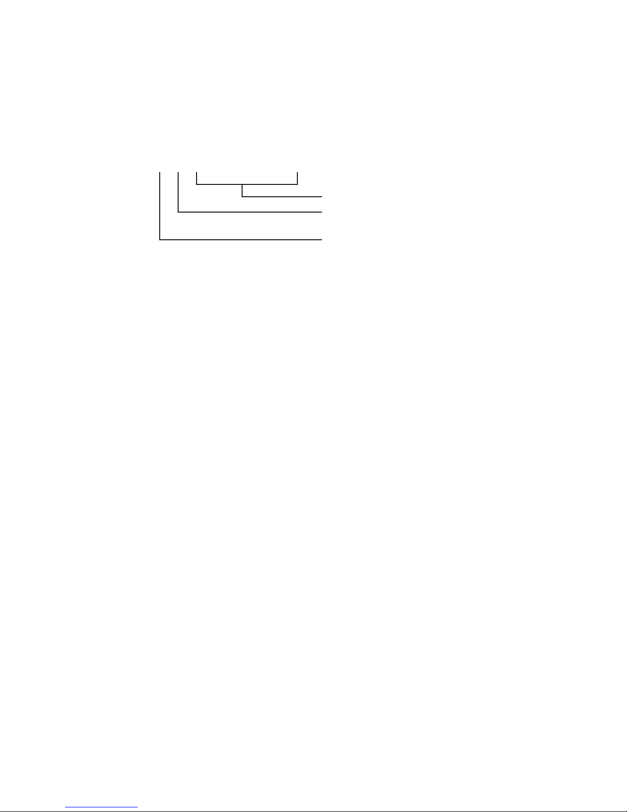
BACKPLANE TIMING
GENERATION
Generating 7M
DOE, ASDELAYED*,
ASQ90*
Clock Buffers
The clock buffers for C1 *, C3*, and CDAC were chosen for
minimum propagation delay and minimum skew. Notice that
buffered clocks are passed to the 100 pin edge connectors, but that
the unbuffered clocks are passed to the 86 pin connector that goes
on to the next box in order to minimize propagation delay to the
next backplane.
We generate 7M (equivalent to the processor clock) by:
7M = C1*XNOR C3*
This yields a 7.16Mhz clock which is used to generate ASDELAYED*,
DOE, and ASQ90*. 7M is also passed to the PICs on pin 92 of the
edge connectors, so they will have a cheap clock for accessing the
bus.
DOE (Data output enable) and ASDELAYED* are the compliment of
each other. ASDELAYED* is used in the steering PAL (ASQ =
ASDELAYED in the PAL equations) to time turning on of the data
drivers during a read cycle. DOE is passed to the PICs on pin 93 of
the edge connectors, to tell the PICs when to turn on data drivers
during a read cycle.
Amiga 7M
Backplane 7M
CDAC
AS∗
ASMID∗
ASDELAYED∗
DOE
ASQ90∗
Backplane Timing Signals
139ns
34

EXAMPLE PIC DESIGN
The PIC at System
Startup
Reading the ID
Locations
This section is a description of the schematic for a small 16 kilobyte
RAM board that we designed as our first test PIC for the expansion
architecture. The schematic for this board is Figure A.2, in Appendix
A, It is valuable as an example because it implements all of the basic
features of a slave PIC.
The heart of auto-config is in U1 (address register), U2 (address
comparator), and U3 (ID PAL and control PAL).
When the board comes out of Reset, CONFIG_OUT* is inactive, and
does not pass the config token on to the next PIC. CONFIG_IN* may
or may not be active at first. If it is not active, the board will not respond to any bus cycles. For instance, we can see at U11 that
SLAVE* is disabled when C0NFIG_IN* is inactive (high), because this
does not allow BOARD-SEL* to go active.
In turn, BOARD_SEL* is an input to U3, the control PAL. Without
BOARD_SEL*. all ten of the PAL outputs are held inactive (see PAL
equations for test ram).
Eventually, during execution of the auto config code, CONFIG_IN*
will be asserted to this PIC between bus cycles (AS* inactive). Notice
that the address latch is tri-stated off so that the pull-up and pulldown resistors are inputing a pattern of E8 to the address comparator. When the backplane addresses E8xxxx, this board will now respond because CONFIG_IN* is active but CONFIG_OUT* is not yet
active. In other words, CONFIG_IN* is enabling board select, and
CONFIG-OUT* has not yet allowed the address latch to move the
board to a different address space.
Notice that whenever BOARD_SEL* goes active, SLAVE* will go active unless SHUT_UP_FOREVER is latched active. SHUT_UP_FOREVER* is a feedback latch in the PAL. It is only set by the software if
the board cannot be configured into the system (for instance, if the
user has plugged in too many large address space PICs and there is
no room left for this one).
If you analyze the PAL equations for BD15 through BD12, you will
see that their data drivers turn on for all reads ANDed with BOARD_SEL active, until CONFIG_OUT* is set active (or some exception
happens such as reset, bus error, or shutup).
By the way, if you're not used to PALs. it's normal old Boolean: *
means AND,/is negation. + is OR, IF(term) means "If the term evaluates to TRUE then turn on the tri-state driver".
35

Further analysis of the BD15-BD12 equations will show that almost
all addresses put out ones; however, remember that most of the
nibbles are inverted because the spec says they have to be. The
inversion makes it possible to implement the codes in active low
PALs; it is just a cost reduction.
Analysis of the equations shows that the only nibbles (we don't care
about above HEX 80) outputting any zeros are:
00/02 1100 0001
04/06 1111 1001
10/12 1111 1110
40/42 0000 0000
To interpret this code, we need to remember that the spec says that
all nibbles get inverted except 00,02,40, and 42. So our new table
looks like this:
00/02 1100 0001
04/06 0000 0110
10/12 0000 0001
40/42 0000 0000
And all the other nibbles that were ones are now inverted to zeros.
To illustrate, let's look at what these codes mean:
00000
111
010
0
0
0
11
00/02
Nibble
Data
04/06
10/12 0000
0000 0110
0001
= 64 kilobytes, the smallest size that
can be requested
= There are no more PICs on this physical
board. It is possible to put more than
one PIC on a physical board, but in
most cases (including this one), we don't.
= This board does not have any Init or
diagnostic code.
= Don't link into memory free list, since
the processor might try to use it
and it is only 16 kilobytes masquerading to
the system as 64 kilobytes.
= Required by the spec.
= Product number = 6
= High byte of manufacturer's number
36

14/16 0000 0000 = Low byte of manufacturer's number
40/42 0000 0000
= Because this PIC does not generate INTs
Passing CONFIG-OUT*
When you want to program your own ID PAL, just work back to the
equations. First determine what ID pattern you need by reading
about the nibbles in the spec. Write down a table of ones and zeros.
Invert all of these except nibbles 00, 02, 40, and 42. Then, doing
one data line at time, write a product term for each binary zero that
you want to output from the ID PAL.
The equations for CONFIG_OUT* in this implementation make two
feedback latches in the PAL. The first latch PRE_C0NFIG_OUT* is set
during the bus cycle in which the processor does a write to the address register. In fact, in this design the rising edge of PRE_CONFIG_OUT latches the final Address value into the address latch.
The second latch outputs CONFIG_OUT*. This latch goes active after
AS* goes inactive at the end of the bus cycle in which the new address was written. Notice that CONFIG-OUT* enables the address
latch Ul. so it now provides the new address range to the comparator.
CONFIG_OUT* enables the next PIC in the chain, and remains active
until a system reset or power down occurs.
TABLE 3-1—TIMING SPECIFICATIONS
Timing Requirements for Backplane
TIMING REQUIREMENTS FOR BACKPLANE
Num Characteristic Min Max Unit
1
2
3
4
5
6
AS* UDS* LDS* Delay
Address 23-1 delay
7M(S4 RISE) to Data Enable during Read
7M (S4 RISE) to Data Valid
Data 15-0 Delay to Output
SLAVEIN or SLAVE to SLAVEOUT Delay
2
2
0
0
8
8
35
8
25
ns
ns
ns
ns
ns
ns
37

Timing Requirements for PIC
TIMING REQUIREMENTS FOR PIC AS SLAVE (RD & WR CYCLES)
Num Characteristic Min Max Unit
1
2
3
4
5
6
AS* low to SLAVE* Low
AS* high to SLAVE* high
AS* low to XRDY low (to insert wait)
Read Data Valid to local 7M low (S7)
AS* low to OVR* low
AS* high to OVR* high
0
0
0
60
0
0
35
50
60
50
50
ns
ns
ns
ns
ns
ns
TIMING REQUIREMENTS FOR PIC AS MASTER (RD & WR CYCLES)
Num Characteristic Min Max Unit
1
2
3
7M high(S2) to AS* low
Address 23-1 Valid to AS* low
7M high (S4) to Data Valid Wr Cycle
0
30
67
0
ns
ns
ns
Timing to Backplane
TIMING TO BACKPLANE
Num Characteristic Min Max Unit
1
2
AS* Low to CDAC Low (Setup)
AS* High to CDAC High (Setup)
20
20
ns
ns
Timing to PIC
TIMING TO PIC (PIC IN SLAVE MODE)
Num Characteristic Min Max Unit
1
2
Valid Address to AS* Low
Data from 7M High(S4) on Wr to PIC
10
35
ns
ns
TIMING TO PIC (PIC IN MASTER MODE)
Num Characteristic Min Max Unit
1 Valid Data setup to Local 7M low(S7) 15 ns
38

2000 SYSTEM BUS
LOADING
The following numbers and notations are used for standard load and
drive values:
Type
From A2000
(IC input load)
To A2000
(IC output drive)
F-Driver TTL
F-Series TTL
LS-DriverTTL
LS-Series TTL
MOS
Open Collector
FD
F
LSD
LS
MOS
20μA@ 2.7V
-1.6mA @ 0.5V
20
ΜA@ 2.7V
-0.6mA @ 0.5V
20
ΜA@ 2.7V
-0.4mA @ 0.4V
20
ΜA@ 2.7V
-0.4mA @ 0.4V
10
ΜA@ 2.4V
-10μA@ 0.4V
fd
f
lsd
ls
mos
oc
2.0V @ -15mA
0.5V @ 64mA
2.7V @ -1mA
0.5V @ 20mA
2.0V @ -15mA
0.5V @ 24mA
2.7V @ -400μA
0.5V @ 8mA
2.4V @ -200
ΜA
0.4V @ 3.2mA
FROM RESISTOR
0.5V @ 8mA
Any lesser input load can be used on a signal in place of a greater
load or equivalent load. Varying the number of load elements while
still meeting the DC loading criteria can be done if necessary, but it
is not a good idea, as it can still exceed the expected capacitive
loading on the signal.
A final type of drive is the open collector (oc). Some PIC outputs
must be open collector, as they are in a wired-or configuration with
the same output from other PICs or motherboard signals.
Most of the system bus signals provide a standard drive to their respective connectors. If your drivers can meet the input specification,
don't worry about what is actually required. However, even if your
loading doesn't exceed the specified drive capacity of slot signal
mentioned above, consult the following chart for specific signals that
may provide less drive than a standard signal of that type. Signals
that match the STANDARD loading are not separately listed.
Named
Signals DIR
Expansion
Slots (each)
Coprocessor
Slot
Video
Slot
STANDARD I 2F 1F 1F
STANDARD 0 10f 10f 10f
/DTACK I 1F 1F
010f 10f
/OVR 0 oc oc
XRDY 0 oc oc
/INT2 0 oc oc
/INT6 0 oc oc
/EINT1 0 oc
/EINT4 0 oc
/EINT5 0 oc
39

Named
Signals
DIR Expansion
Slots (each)
Coprocessor
Slot
Video
Slot
/EINT7 0 oc
/SLAVEn 0 2f
/CFGOUTn 0 2f
/COPCFG 0 2f
E Clock I 1F 1F
7MHz Clock I 1F 1F
/BERR I 1F 1F
0oc oc
/VPA I 1F 1F
0oc oc
/VMA I 1F 1F
0 10f 10f
/RST I 1F 1F
0oc oc
/HLT I 1F 1F
0oc oc
/OWN 0 oc
/BRn 0 2f
/CBR I 2F
02f
/CBG I 2F
02f
/BGACK I 1F 1F
0oc oc
/BOSS 0 2f
XCLK 0 2f
/XCLKEN 0 2f
40

TABLE 3-2
PAL16L8
STEERING150R17REV3
11-17-85
AMIGA
/SLVOUT RD /ASQ /ASQ90 COLLIS /BG /AS /BGACK /DMAIN GND
/OWN /AOE /UDS /BERR /DMAOUT /LDS /DBOE /RES /D2P VCC
DBOE = AS * /RD * /BERR + ;DATA DRIVERS DURING WRITE CYCLE
UDS * RD * ASQ * /BERR + ;TURN ON DRIVERS LATE FOR RD
LDS* RD* ASQ* /BERR UDS AND LDS PROTECT RD MOD WR
;TO AVOID TRI STATE FIGHT
D2P = /DMAOUT * SLVOUT * RD + ;DOWNSTREAM READS UPSTREAM SLAVE
DMAOUT * /SLVOUT * /RD + ;UPSTREAM WRITES DOWNSTREAM SLAVE
DMAOUT* SLVOUT ;MASTER AND SLAVE ARE UPSTREAM
AOE = BGACK +
/BG * /DMAOUT + ;AS KEEPS ADDR WHEN /BG DROPS
AS + ;ASQ90 MAINTAINS VALID ADDR ON
ASQ90 ; LAST PROC CYCLE
DMAOUT = DMAIN + OWN
IF (/RES * COLLIS) BERR = VCC
DESCRIPTION
SLVOUT = SLAVEOUT,ASQ = AS DELAYED,ASQ90 = AS CLKD ON LOW EDGE OF 7M.
BG = BUS GRANT,OWN = LOCAL OWN
COLLIS = BUS COLLISION,AOE = ADDR OUTPUT EN,DOE = DATA OE
RES = RESET,D2P=DATAT0 PROCESSOR
UDS LDS PROTECT AGAINST RDMODIFYWRITE 3STF1GHT & BERR= /DOE
41

TABLE 3-3
PAL16R6
ARBITRATE REV1
1-6-86
AMIGA
7M /BRIN /RES /BGiN /BR5 /BR4 /BR3 /BR2 /BR1 GND
GROUND /BGOUT /BGOLD /BG5 /BG4 /BG3 /BG2 /BG1 /BR VCC
BG1 = BGIN * /BGOLD * BR1 * /RES + GENERATE BG1
BGIN * BG1 * /RES ;HOLD UNTIL /BG
BG2 = BGIN * /BGOLD • BR2 * /BRl * /RES +
BGIN * BG2 * /RES
BG3 = BGIN * /BGOLD * BR3 * /BRl * /BR2* /RES +
BGIN * BG3 * /RES
BG4 = BGIN * /BGOLD * BR4 * /BR1 * /BR2 * /BR3 * /RES +
BGIN * BG4 * /RES
BG5 = BGIN * /BGOLD * BR5 * /BR1 * /BR2 • /BR3 * /BR4 * /RES +
BGIN * BG5 • /RES
BGOLD = BGIN STORE OLD STATE OF BG
BR = BRIN * /RES + ' ;BR IS RQST TO 68K
BR1 */RES + BR2 * /RES +
BR3 * /RES + BR4 * /RES
+ BR5 */RES
BGOUT = BGIN* BGOLD*/BGl * /BG2 * /BG3 * /BG4 * /BG5
DESCRIPTION
BG1 IS HIGHEST PRIORITY
42

TABLE 3-4
PAL20L10
TESTRAM
9-11-85
COMMODORE-AMIGA
/ASQ /ASQQ RD /BDSEL /BERR A6 A5 A4 A3 A2
A1 GND/RES BD12 BD13 BD14 BD15/PRECON /CONOUT /SHUTUP
/RAMOE /WP /DBOE VCC
DBOE = /RES*BDSEL*/BERR*/SHUTUP*/RD + ;WRITES TURN ON
EARLY
/RES*BDSEL*/BERR*SHUTUP* RD*ASQ ;ASQ DELAYS THE READ
WP = /RES*ASQ*ASQQ*BDSEL*CONOUT*/SHUTUP*/RD*/BERR
RAMOE = /RES*ASQ*RD*CONOUT*/BERR*BDSEL
SHUTUP = /RES*BDSEL*/RD*ASQ*/CONOUT*A6*/A5*/A4*A3*A2 +
/RES*SHUTUP
PRECON = /RES*SHUTUP +
/RESVRD*BDSEL*ASQQ*A6*/A5*/AD*A3*/A2*/A1 +
/RES*PRECON
CONOUT = /RES*ASQ*PRECON +
/RES*CONOUT
IF (/RES*BDSEL*/CONOUT*RD*/BERR*/SHUTUP) /BD15 =
/A6*/A5*/A4*/A3*/A2*A1 +
A6*/A5*/A4*/A3*/A2
IF (/RES*BDSEL*/C0N0UT*RD*/BERR*/SHUTUP)/BD14 =
/A6*/A5*/A4*/A3*A1 +
A6*/A5*/A4*/A3*/A2
IF (/RES*BDSEL*/CONOUT*RD*/BERR*/SHUTUP) /BD13 =
/A6*/A5*/A4*/A3*/A2 +
/A6*/A5*/A4*/A3*A2*A1 +
A6*/A5*/A4*/A3*/A2
IF (/RES*BDSEL*/CONOUT*RD*/BERR*/SHUTUP) /BD12 =
/A6*/A5*/A4*/A3*/A2*/A1 +
/A6*/A5*A4*/A3*/A2*A1 +
A6VA5*/A4*/A3*/A2
DESCRIPTION
43

TABLE 3-5
PAL16L8
COLLISION
11-17-8S
AMIGA
/BAS /SLV1 /SLV2 /SLV3 /SLV4 /SLV5 /SLVIN A23 A22 GND
A21 /SLVOUT A20 A19 /OVR /RESET P17 /PROC /NOTCOLIS VCC
SLVOUT = SLV1 + SLV2 + SLV3 + SLV4 + SLV5 + SLVIN
NOTCOLIS = /SLV1 * /SLV2 * /SLV3 * /SLV4 * /SLV5 * /SLVIN +
/PROC * /SLV2 * /SLV3 * /SLV4 * /SLV5 * /SLVIN +
/PROC * /SLV1 * /SLV3 * /SLV4 * /SLV5 * /SLVIN +
/PROC * /SLV1 * /SLV2 * /SLV4 * /SLV5 * /SLVIN +
/PROC * /SLV1 * /SLV2 * /SLV3 * /SLV5 * /SLVIN +
/PROC * /SLV1 * /SLV2 * /SLV3 * /SLV4 * /SLVIN +
/PROC * /SLV1 * /SLV2 * /SLV3 * /SLV4 * /SLV5
PROC = BAS * /A23 * /A22 * /A21 * /RESET * /OVR +
BAS * A23 * /A22 * A21 * /RESET * /OVR +
BAS * A23 * A22 * /A21 * /RESET * /OVR +
BAS * A23 * A22 * A21 * /A20 * /A19 * /RESET * /OVR +
BAS* A23 * A22 * A21 * A2O * A19 * /RESET * /OVR
DESCRIPTION
EMPTY
44

INTERFACING TO THE
68K BUS CONNECTOR
ON THE AMIGA 500
TIMING
Clocks
This section gives the necessary information for interfacing to the
68000 bus connector on the left side of the Amiga A500 (or the
right side of the A1000).
THE CONNECTOR ON THE AMIGA
The connector is a standard dual row 86 finger (43 on a side) edge
connector, spaced on .1" centers. Here are some part numbers of
connectors that are compatible:
solder tail AMP 2-530841-1 wire
wrap AMP 4-530396-7 card extender
AMP 1-530826-2
See accompanying drawing for physical dimensions of this connector
on the A500, Figure A-3 in Appendix A.
For this discussion, see Figure 3.2.
The entire computer board is run synchronously to the 3.57954Mhz
color clock (C1). This is accomplished by generating a number of
sub-multiple frequencies from our master 28.63636Mhz crystal oscillator. The following are the primary clocks on the board:
Name Description
C1 The 3.579545Mhz Color Clock
C2 C1 shifted 45 degrees later
C3 C1 shifted 90 degrees later
C4 C1 shifted 135 degrees later
7M C1 XORed with C3* (7,15909Mhz)
DAC 7M shifted 90 degrees later
7M is the processor clock for the 68000 microprocessor. C1 -C4
and DAC are used to clock the custom chips and for determining the
timing of signals to the memory arrays.
The above frequencies are true for NTSC Amigas. A PAL Amiga will
operate slightly slower, with a main clock of 28.37516Mhz. This is
divided down to get 7M = 7.09379Mhz and C1 = 3.546895Mhz. A
special circuit is required to take five fourths of C1 to derive the PAL
colorburst frequency of 4.43361875Mhz.
The following clocks are available at the edge connector:
Name Pin Description
C3* 14 C3 inverted
CDAC 15 DAC equivalent
Cl* 16 C1 inverted
Note that 7M {the processor clock) is not available at the connector;
it can be easily generated by:
C3*XNOR C1* = 7M equivalent
45

If you need a 14.31818Mhz synchronous clock, you can generate it
by:
(7Mequiv) XOR (CDAC) = 14M equivalent
~139ns
SyncdS2
1 s t Q r t l
Fig. 3.2 Amiga System Clocks
14M
CDAC
7M
C1
C2
C3
C4
C1∗
C3∗
Bus Timing
The 68000 is connected directly to the 86 pin connector, there are
no buffers between the 68000 and the connector. Two control inputs, VPA* and DTACK* are driven by logic on the Amiga and should
not be driven by your circuitry, unless OVR* is used to disable this
logic.
Many boxes are being designed which pass the bus (buffered) out in
daisy chain fashion.
In order to allow your device to be the second in the chain, take into
account an extra level of signal buffers on:
AS*, UDS*. LDS*. Address. Data. Clocks
Furthermore, if you are designing a DMA device, the Amiga provides
data in response to a Read very late (50ns prior to the fall of S6). If
your DMA device is looking at this data through two or three
74F245's (7ns each), this data will not be valid at your DMA
controller until approximately 25ns prior to the fall of S6.
46

Slave Bus Timing
CPU bus timing is based on an 8Mhz 68000, with only one exception: under normal operation, the bus control PAL asserts DTACK*
for you. DO NOT ASSERT DTACK*; do not attach any outputs to the
DTACK* line.
Details of 68000 timing are available in the Motorola 68000 hardware manual. If you are designing a bus slave, most bus timing is
per the 68000 spec, except that the CPU will pull DTACK* for you.
If you need to delay our assertion of DTACK*. you must pull XRDY
(Pin 18) no later than 60ns after the assertion of AS*. You should
release XRDY when you are ready to complete the bus cycle.
Also remember that in the expansion architecture, data drivers
should not turn on during a Read cycle until S4.
For those of you who have not designed anything on the 68K bus
before, this description is intended to make looking at the Motorola
timing diagrams easier. For more details and timing specs see
Motorola hardware manual (fold out timing diagrams in the back of
the book.)
See Figure 3.2 in this section. Motorola labels the states of the processor clock S0-S7. The processor starts driving the address lines
during S1, and asserts AS* (Address Strobe) during S2. If the cycle
is a read, the data strobes (UDS*,LDS*) are asserted during S2 also
(they are delayed until S4 on a write).
The board responds to AS* by asserting DTACK* (unless you delay
DTACK by pulling XRDY low). In order to run a normal 4 clock bus
cycle, DTACK* meets the setup time prior to S5. DTACK* is the acknowledge to the bus cycle. If DTACK* is not asserted, the 68000
stays in the middle of the bus cycle until DTACK* (or BERR* or
VPA*) is asserted. Once DTACK* is asserted, the processor
completes the read (or write) and ends the cycle by disasserting the
strobes (AS*,UDS*.LDS*) and tri-stating its bus drivers.
If the slave you are designing cannot respond fast enough to
successfully complete a 4 clock bus cycle, it must pull XRDY low
within 60ns after the assertion of AS* (and of course the correct
address). Our board then will not assert DTACK* until you release
XRDY. You should drive XRDY with an open collector output; we
provide a 1K pullup resistor on our board.
47

XXXXXX XXXX
Fig. 3.3 Standard 4 Clock Read Cycle
XXXXXXX XXXX
S0 S1 S2 S3 S4 S5 S6 S7 S0 etc
7M = CLK
A23-A1
AS*
UDS ,LDS**
D15-D0
R/W
DTACK*
XXXXX
XXX
Fig. 3.4 Standard 4 Clock Write Cycle
XXXXXXX
XXXX
S0 S1 S2 S3 S4 S5 S6 S7 S0 etc
7M = CLK
A23-A1
AS*
UDS ,LDS**
D15-D0
R/W
DTACK*
48

XXXX
60ns max
XXX
XXXX
XXXXXXX
S0
S1
S2 S3 S4 SW SW S5 S6 S7 S0 etc
7M = CLK
A23-A1
AS∗
XRDY
DTACK∗
D15-D0
Fig. 3.5 Using XRDY to Delay DTACK*
Master Bus Timing
BGACK* and OWN*
Timing to Avoid Bus
Contention
All bus masters must run synchronously to 7M (equivalent), as does
the 68000 in the Amiga.
The necessary information for designing a bus master is in the
68000 hardware manual. A master must meet all of the bus timing
specs of an 8Mhz 68000; for example, valid address must precede
AS* by at least 30ns.
If you are designing a bus master card that will plug into a box, remember that the address will have to propagate through the
address drivers built into the box; you should probably allow for the
prop delay of three 74F245's in addition to the required 30ns.
The strobes, such as AS*,UDS*,LDS*. must all function as they
would basically on the 68000 spec. A master must also respond to
DTACK*, HALT*, and BERR* correctly.
The basic timing for bus arbitration conforms very closely to the
68000 and the 68440. When the new master has received BG* and
all other signals necessary to take mastership, it must assert OWN*
before it asserts BGACK*. This gives the address drivers on the bus
time to change direction, if necessary, before BGACK* turns them
on.
At the end of the DMA cycle, BGACK* must be disasserted before
OWN* is disasserted.
BR* should always be asserted off the rising edge of 7M, and should
be valid no later than 60ns after that edge.
49

50

Section 3.2
Driver documentation
OVERVIEW
This section discusses how the "binddrivers" program finds your
driver and links it into the system. It also hints on how to write your
code to take advantage of this.
First off. the expansion library goes out and configures the expansion boards in the system. It puts each board in its own address
space, and links memory boards into the memory free pool. This is
done by the expansion.library's ConfigChain entry point. This code is
intended to be run early on in system startup, before any other code
is around.
Later on, after the DOS is running, the binddrivers program should
be run. This program searches the directory "SYS:Expansion" for
workbench icon files. If it finds one with a tooltypes variable "PRODUCT" then it parses the rest of the line (see below) and looks for an
unconfigured board that matches the description.
This method makes user installation of a new driver trivial: the user
only has to copy a workbench icon into the expansion directory on
his sys disk. Everything else is automatic the next time he boots.
In addition, the bootdrivers program may be run repeatedly without
ill effect. Devices will not be configured twice, so binddrivers may be
run after a new driver is installed (so the user does not have to reboot after installing a driver).
Here is an overview of the process:
search:
for each file that ends in .info, do test ().
test:
1. Call GetDiskObject() on this file. If not a workbench object, re-
turn.
2. Call FindToolType () to see if there is a PRODUCT definition. If
not. Return.
3. If the description does not match an unconfigured board, return.
If there are boards, link them all together and record them in a
static area.
4. LoadSeg () the code file. If LoadSeg fails, return.
5. Search the first hunk for a Resident structure. If no structure,
UnLoadSeg () the segment and return.
51

6. InitResident () the loaded code. If an error (NULL) is returned,
UnLoadSeg () the segment
your driver code:
Find the list of boards. Mark them a configured, and record
your driver in them (for system debugging). Return non-zero
value if everything went ok. If something went wrong (or you
just want to be unloaded) then return NULL.
Now for some more detail.
1. GetDiskObject () is a routine in icon.library. It will read in the disk
object and return a pointer to it. Part of a disk object structure is
a "tooltypes" field.
2. The FindToolType () routine (also in the icon.library) searches the
tooltypes database associated with the disk object If there is an
entry for PRODUCT then it is assumed that this is an info file for
a driver. The PRODUCT field is of the format:
PRODUCT = <idlist>
<idlist> ::= <id> | <idlist>BAR<id>
<id> ::= <manufacturer> | < manufactured SLASH <product>
<manufacturer> ::= <a decimal number>
<product> ::= <a decimal number>
BAR :: = <a vertical bar — "|'>
SLASH ::= <a forwards slant char — "/'>
Spaces are not legal. Some examples:
PRODUCT = 1000/30 ; matches man 1000, product 30
PRODUCT = 1000 ; matches any man 1000 board
PRODUCT = 1000/20| 1000/21; matches man 1000, product 20
or 21
3. Each unconfigured board in the system is searched. An unconfi-
gured board has the CDB_CONFIGME bit set in the ccLFIags byte.
Search all these unconfigured boards to find the ones that match
any of the product codes. Link all these boards together using the
ccLNextCD field of the ConFigDev structure. Record the head of
this list, along with the product field and the name of the file that
was loaded in a CurrentBinding structure. This structure may be
retrieved via the GetCurrentBinding () call.
4. Attempt to load in the driver. The driver may be a devices,
library, task, process, or anything else that you may want. The
only requirement is that it have a Resident structure in its first
hunk. (By the way, this means that you can not directly use
startup.obj).
52

HINTS FOR WRITING
YOUR DRIVER CODE:
This is why we refer to loading a "driver'" rather than a "device"
— you can write any sort of code you want to handle your device.
5. Binddriver will search the first hunk for a Resident structure. If it
cannot find one, it will assume some awful mistake has been
made, and will unload the segment
6. Finally we get to running some of YOUR code. InitResident () is
used to start you off and running. The return value from InitResident (and therefore the return value from your init entry point)
will be checked on exit. If it is zero then the segment will be unloaded. This can be useful if you only need to do a bit of initialization and then can go away, such as allocate additional expansion
memory for a non-expansion architecture board.
Your driver will be launched via InitResident () as discussed above.
If you use the underdocumented. but very useful RTF_AU-TOINIT
option you will have a library node constructed for you. and then
have the code you specified enter. If you don't use
RTF_AUTOINIT. then your code will be entered directly.
You should (among everything else you might be doing) open the
expansion.library and ask for the current buildings (GetCurrentBindingO). In this structure will be the head of a singly linked list
of ConfigDev structures. The structures are linked via the cd
NextCD field. You should deal with each member of the list —
they are for you!
There are two actions you must take. One is to unset the CDB
CONFIGME bit in the cd_Flags. If you do not do this then the
board is still available for other drivers (of course, you may actually want this .. .). If you do unset the CONFIGME bit, please also
record your "node" in the ccLDriver structure. It is assumed that
this is in an exec node, whose LN_NAME field points your name,
and LN_TYPE field is your type of "thing" — library, resource,
device, task, etc. I know that this will not always apply to you, but
try it anyway. It will help the rest of us debug the system when
something goes wrong.
You have now done everything you wanted to. Your init routine is
about to return. If you return a zero, then your code will be unloaded. If you return non-zero, then you will stay around
53

54

Section 3.3
Software for Amiga Expansion
EXPANSION.LIBRARY/
ADDDOSNODE
This section contains listings and information on the following
expansion software commands:
expansion.library/AddDosNode expansion.library/MakeDosNode
System/Libraries/Expansion/AddConfigDev
System/Libraries/Expansion/AllocBoardMem
System/Libraries/Expansion/AUocConfigDev
System/Libraries/Expansion/AllocExpansionMem
System/Libraries/Expansion/ConfigBoard
System/Libraries/Expansion/ConfigChain
System/Libraries/Expansion/FindConfigDev
System/Libraries/Expansion/FreeBoardMem
System/Libraries/Expansion/FreeConfigDev
System/Libraries/Expansion/FreeExpansionMem
System/Libraries/Expansion/GetCurrentBinding
System/Libraries/Expansion/ObtainConfigBinding
System/Libraries/Expansion/ReadExpansionByte
System/Libraries/Expansion/ReadExpansionRom
System/Libraries/Expansion/ReleaseConfigBinding
System/Libraries/Expansion/RemConfigDev
System/Libraries/Expansion/SetCurrentBinding
System/Libraries/ExpansionA/VriteExpansionByte
NAME
AddDosNode — mount a disk to the system
SYNOPSIS
ok = AddDosNode( bootPri, flags, deviceNode )
DO DO D1 AO
FUNCTION
This routine makes sure that your disk device (or a device that
wants to be treated as if it was a disk...) will be entered into the
system. If the dos is already up and running, then it will be entered
immediately. If the dos has not yet been run then the data will be
recorded, and the dos will get it later.
55

We hope to eventually try and boot off a disk device. We will try and
boot off of each device in turn, based on priority, if there is no boot
floppy in the floppy disk drive. As of this writing that facility does
not yet exist.
There is only one additional piece of magic done by AddDosNode. If
there is no executable code specified in the deviceNode structure
(e.g. dn_SegUst, dn_Handler, and dn_Task are all null) then the
standard dos file handler is used for your device.
Documentation note: a "task" as used here is a dos-task, not an
exec-task. A dos-task, in the strictest sense, is the "address of an
exec-style message port. In general, it is a pointer to a process's
pr_MsgPort field (e.g. a constant number of bytes after an exec
port).
INPUTS
bootPri — a BYTE quantity with the boot priority for this disk.
This priority is only for which disks should be looked at: the actual
disk booted from will be the first disk with a valid boot block. If
no disk is found then the "bootme" hand will come up and the
bootstrap code will wait for a floppy to be inserted. Recommend
priority assignments are:
+ 5 — unit zero for the floppy disk. The floppy should always
be highest priority to allow the user to abort out of a hard disk
boot.
0 — the run of the mill hard disk
-5 — a "network" disk (local disks should take priority).
-128 — don't even bother to boot from this device.
flags — additional flag bits for the call:
ADN_TARTPROC (bit 0) — start a handler process imme-
diately.
Normally the process is started only when the device node is
first referenced. This bit is meaningless if you have already
specified a handler process (non-null dn_Task).
deviceNode — a legal DOS device node, properly initialized.
Typically this will be the result of a MakeDosNode() call, but feel
free to manufacture your own if you need to. If deviceNode is null
then AddDosNode does nothing.
RESULTS
ok - non-zero everything went ok, zero if we ran out of memory or
some other weirdness happened.
56

EXPANSI0N.LIBRARY/
MAKEDOSNODE
EXAMPLES
/* enter a bootable disk into the system. Start a file handler
** process immediately.
*/
AddDosNode( 0, ADNF_STARTPROC, MakeDosNode( paramPacket)
);
BUGS
The flexible boot strategy is only that — strategy. It still needs to be
reflected in code somewhere.
SEE ALSO
MakeDosNode
NAME
MakeDosNode — construct dos data structures that a disk needs
SYNOPSIS
deviceNode = MakeDosNode( parameterPkt)
DO AO
FUNCTION
This routine manufactures the data structures needed to enter a dos
disk device into the system. This consists of a DeviceNode, a
FileSysStartupMsg, a disk environment vector, and up to two bcpl
strings. See the libraries/dosextens and tibraries/filehandler include
files for more information.
MakeDosNode will allocate all the memory it needs, and then link
the various structure together. It will make sure all the structures
are long-word aligned (as required by the DOS). It then returns the
information to the user so he can change anything else that needs
changing. Typically he will then call AddDosNode() to enter the new
device into the dos tables.
INPUTS
parameterPkt - a longword array containing all the information
needed to initialize the data structures. Normally I would have provided a structure for this, but the variable length of the packet
caused problems. The two strings are null terminated strings, like all
other exec strings.
57

longword description
0 string with dos handler name
1 string with exec device name
2 unit number (for OpenDevice)
3 flags (for OpenDevice)
4 # of longwords in rest of environment
5-n file handler environment (see libraries/file-
handler.h)
RESULTS
deviceNode — pointer to initialize device node structure, or null if
there was not enough memory.
EXAMPLES
/* set up a 3.5" amiga format floppy drive for unit 1 */
char execName[] = "trackdisk.device";
char dosName[] = "df1";
ULONG parmPkt[] = [
(ULONG) dosName,
(ULONG) execName,
1, /* unit number */
0, /* OpenDevice flags */
/* here is the environment block */
11, /* table upper bound */
512>>2, /* # longwords in a block */
0, /* sector origin — unused */
2, /* number of surfaces */
1, /* secs per logical block— unused */
11, /* secs per track */
2, /* reserved blocks — 2 boot blocks */
0, /*?? — unused */
0, /* interleave */
0, /* lower cylinder */
79, /* upper cylinder */
5, /* number of buffers */
];
struct Device Node *node, *MakeDosNode();
node = MakeDosNode( parmPkt):
BUGS
SEE ALSO
AddDosNode
58

SYSTEM/LIBRARIES/
EXPANSION/
ADDCONFIGDEV
SYSTEM/LIBRARIES/
EXPANSION/
ALLOCBOARDMEM
NAME
AddConfigDev — add a new ConfigDev structure to the system
SYNOPSIS
AddConfigDev( configDev)
AO
FUNCTION
This routine adds the specified ConfigDev structure to the list of
Configuration Devices in the system.
INPUTS
configDev — a valid ConfigDev structure.
RESULTS
EXCEPTIONS
SEE ALSO
RemConfigDev
BUGS
NAME
AllocBoardMem — allocate standard device expansion memory
SYNOPSIS
startSlot = AllocBoardMem( slotSpec)
DO DO
FUNCTION
This function allocates numslots of expansion space (each slot is
E_SLOTSIZE bytes). It returns the slot number of the start of the
expansion memory. The EC_MEMADDR macro may be used to
convert this to a memory address.
AllocBoardMem{) knows about the intracacies of expansion board
hardware and will allocate the proper expansion memory for each
board type.
59

SYSTEM/LIBRARIES/
EXPANSION/
ALLOCCONFIGDEV
INPUTS
slotSpec — the memory size field of the Type byte of an expansion
board
RESULTS
startSlot — the slot number that was allocated, or -1 for error.
EXAMPLES
struct ExpansionRom *er;
slot = AllocBoardMemf er->er_Type & ERT_MEMMASK )
EXCEPTIONS
SEE ALSO
AllocExpansionMem. FreeExpansionMem. FreeBoardMem
BUGS
NAME
AllocConfigDev — allocate a ConfigDev structure
SYNOPSIS
configDev = AllocConfigDev()
DO
FUNCTION
This routine returns the address of a ConfigDev structure. It is provided so new fields can be added to the structure without breaking
old. existing code. The structure is cleared when it is returned to the
user.
INPUTS
RESULTS
configDev — either a valid ConfigDev structure or NULL.
EXCEPTIONS
60

SYSTEM/LIBRARIES/
EXPANSION/
ALLOCEXPANSIONMEM
SEE ALSO
FreeConfigDev
BUGS
NAME
AllocExpansionMem — allocate expansion memory
SYNOPSIS
startSlot = AllocExpansionMem( numSlots. slotOffset)
DO DO D1
FUNCTION
This function allocates numslots of expansion space (each slot is
E_SLOTSIZE bytes). It returns the slot number of the start of the
expansion memory. The EC_£MADDR macro may be used to convert
this to a memory address.
Boards that fit the expansion architecture have alignment rules.
Normally a board must be on a binary boundary of its size. Four and
Eight megabyte boards have special rules. User defined boards
might have other special rules.
The routine AllocBoardMem() knows about all the allocation rules
for standard boards. Most users will want to use that routine if they
want memory for a standard expansion device.
if AllocExpansionMem() succeeds, the startSlot will satisfy the
following equation:
(startSlot — slotOffset) MOD slotAlign = 0
INPUTS
numSlots — the number of slots required.
slotOffset — an offset from that boundary for startSlot.
RESULTS
startSlot — the slot number that was allocated, or -1 for error
61

SYSTEM/LIBRARIES/
EXPANSION/
CONFIGBOARD
EXAMPLES
AllocExpansionMem( 2,0)
Tries to allocate 2 slots on a two slot boundary.
AllocExpansionMem( 64, 32)
This is the allocation rule for 4 meg boards. It allocates 4 megabytes
(64 slots) on an odd 2 meg boundary.
EXCEPTIONS
SEE ALSO
FreeExpansionMem, AllocBoardMem, FreeBoardMem
BUGS
NAME
ConfigBoard — configure a board
SYNOPSIS
error = ConfigBoard( board. configDev )
DOAO A1
FUNCTION
This routine configures an expansion board. The board will generally
live at ELEXPANSIONBASE, but the base is passed as a parameter to
allow future compatibility. The configDev parameter must be a valid
configDev that has already had ReadExpansionRom() called on it
ConfigBoard will allocate expansion memory and place the board at
its new address. It will update configDev accordingly. If there is not
enough expansion memory for this board then an error will be returned.
INPUTS
board — the current address that the expansion board is responding.
configDev — an initialized ConfigDev structure.
RESULTS
error — non-zero if there was a problem configuring this board
62

SYSTEM/LIBRARIES/
EXPANSION/
CONFIGCHAIN
EXCEPTIONS
SEE ALSO
FreeConfigDev
BUGS
NAME
ConfigChain — configure the whole damn system
SYNOPSIS
error = ConfigChain( baseAddr)
DO AO
FUNCTION
This is the big one! This routine will take a base address (generally
E_EXPANSIONBASE) and configure all the devices that live there.
This routine will call all the other routines that might need to be
called. All boards that are found will be linked into the configuration
list
INPUTS
baseAddr — the base address to start looking for boards.
RESULTS
error — non-zero if something went wrong.
EXCEPTIONS
SEE ALSO
FreeConfigDev
BUGS
63

SYSTEM/LIBRARIES/
EXPANSION/
FINDCONFIGDEV
NAME
FindConfigDev — find a matching ConfigDev entry
SYNOPSIS
configDev = FindConfigDev( oldConfigDev. manufacturer, product)
DO AO DO D1
FUNCTION
This routine searches the list of existing ConfigDev structures in the
system and looks for one that has the specified manufacturer and
product codes.
If the oldConfigDev is NULL the the search is from the start of the
list of configuration devices. If it is not null then it searches from the
first configuration device entry AFTER oldConfigDev.
A code of -1 is treated as a wildcard — e.g. it matches any manufacturer (or product)
INPUTS
oldConfigDev — a valid ConfigDev structure, or NULL to start from
the start of the list.
manufacturer — the manufacturer code being searched for. or -1 to
ignore manufacturer numbers.
product — the product code being searched for, or -1 to ignore
product numbers.
RESULTS
configDev — the next ConfigDev entry that matches the manufacturer and product codes, or NULL if there are no more matches.
EXCEPTIONS
EXAMPLES
/* to find all configdevs of the proper type */ struct ConfigDev *cd =
NULL;
while( cd = FindConfigDev( cd. MANUFACTURER. PRODUCT ) ) [
/* do something with the returned ConfigDev */
]
SEE ALSO
BUGS
64

SYSTEM/LIBRARIES/
EXPANSION/
FREEBOARDMEM
NAME
FreeBoardMem — allocate standard device expansion memory
SYNOPSIS
FreeBoardMem( startSlot. SlotSpec )
DO D1
FUNCTION
This function frees numslots of expansion space (each slot is
E_SLOTSIZE bytes)- It is the inverse function of AllocBoardMem().
INPUTS
startSlot — a slot number in expansion space.
slotSpec — the memory size field of the Type byte of an expansion
board
RESULTS
EXAMPLES
struct ExpansionRom *er;
int startSlot;
int slotSpec;
slotSpec = er->er_Type& ERT_MEMMASK:
startSlot = AllocBoardMem( er->er_Type & ERT_MEMMAK );
if( startSlot != -1 ) [
FreeBoardMem( startSlot, slotSpec );
]
EXCEPTIONS
If the caller tries to free a slot that is already in the free list.
FreeBoardMem will Alert() (e.g. crash the system).
SEE ALSO
AllocExpansionMem. FreeExpansionMem. AllocBoardMem
BUGS
65

SYSTEM/LIBRARIES/
EXPANSION/
FREECONFIGDEV
SYSTEM/LIBRARIES/
EXPANSION/
FREEEXPANSIONMEM
NAME
FreeConfigDev — allocate a ConfigDev structure
SYNOPSIS
FreeConfigDev(configDev)
AO
FUNCTION
This routine frees a ConfigDev structure as returned by
AllocConfigDev.
INPUTS
configDev — a valid ConfigDev structure.
RESULTS
EXCEPTIONS
SEE ALSO
AllocConfigDev
BUGS
NAME
FreeExpansionMem — allocate standard device expansion memory
SYNOPSIS
FreeExpansionMem(startSlot, numSlots)
DO D1
FUNCTION
This function allocates numslots of expansion space (each slot is
ELSLOTSIZE bytes). It is the inverse function of
AllocExpansionMem().
INPUTS
startSlot — the slot number that was allocated, or -1 for error.
numSlots — the number of slots to be freed.
RESULTS
66

SYSTEM/LIBRARIES/
EXPANSION/
GETCURRENTBINDING
EXAMPLES
EXCEPTIONS
If the caller tries to free a slot that is already in the free list,
FreeExpansionMem will Alert() (e.g. crash the system).
SEE ALSO
AllocExpansionMem, AllocBoardMem, FreeBoardMem
BUGS
NAME
GetCurrentBinding — sets static board configuration area
SYNOPSIS
actual = GetCurrentBinding( currentBinding, size)
A0D0:16
FUNCTION
This function writes the contents of the ""currentBinding" structure
out of a private place. It may be set via SetCurrentBinding(). This is
really a kludge, but it is the only way to pass extra arguments to a
newly configured device.
A CurrentBinding structure has the name of the currently loaded
file, the product string that was associated with this driver, and a
pointer to the head of a singly linked list of ConfigDev structures
(linked through the cd_NextCD field).
Many devices may not need this information; they have hard coded
into themselves their manufacture number. It is recommended that
you at least check that you can deal with the product code in the
linked ConfigDev structures.
INPUTS
currentBinding — a pointer to a CurrentBinding structure
size — the size of the user's binddriver structure. No more than this
much data will be copied. If size is larger than the libraries idea a
CurrentBinding size, then the structure will be null padded.
67

SYSTEM/LIBRARIES/
EXPANSION/
OBTAINCONFIGBINDIN
G
RESULTS
actual — the true size of a CurrentBinding structure is returned.
EXAMPLES
EXCEPTIONS
SEE ALSO
GetCurrentBinding
BUGS
NAME
ObtainConfigBinding — try to get permission to bind drivers
SYNOPSIS
ObtainConfigBinding()
FUNCTION
ObtainConfigBinding gives permission to bind drivers to ConfigDev
structures. It exists so two drivers at once do not try and own the
same ConfigDev structure. This call will block until it is safe to proceed.
Individual drivers do not need to call this routine. It is intended for
BindDriver program, and others like it. If your drivers wont be loaded via the standard method, you may need to lock out others.
It is crucially important that people lock out others before loading
new drivers. Much of the data that is used to configure things is
statically kept and others need to be kept from using it.
This call is build directly on Exec SignalSemaphore code
(e.g. ObtainSemaphore).
INPUTS
RESULTS
EXCEPTIONS
SEE ALSO
ReleaseConfigBinding
68

SYSTEM/LIBRARIES/
EXPANSION/
READEXPANSIONBYTE
BUGS
NAME
ReadExpansionByte read a byte nybble by nybble.
SYNOPSIS
byte = ReadExpansionByte( board, offset )
DO AO DO
FUNCTION
ReadExpansionByte reads a byte from a new-style expansion board.
These boards have their readable data organized as a series of
nybbles in memory. This routine reads two nybbles and returns the
byte value.
In general, this routine will only be called by ReadExpansionRom.
The offset is a byte offset into a ExpansionRom structure. The
actual memory address read will be four times larger. The macros
EROFFSET and ECOFFSET are provided to help get these offsets
from C.
INPUTS
board —a pointer to the base of a new style expansion board, offset
— a logical offset from the board base
RESULTS
byte — a byte of data from the expansion board, or ■ 1 if there was
an error reading from the board.
EXAMPLES
byte = ReadExpansionByte( cd->BoardAddr. EROFFSET( er_Type ) )
: ints = ReadExpansionByte(cd->BoardAddr, ECOFFSET
(ec_Interrupt));
EXCEPTIONS
SEE ALSO
WriteExpansionByte. ReadExpansionRom
BUGS
69

SYSTEM/LIBRARIES/
EXPANSION/
READEXPANSIONROM
NAME
ReadExpansionRom— read a board's configuration ROM space
SYNOPSIS
error = ReadExpansionRom( board, configDev )
DO AO A1
FUNCTION
ReadExpansionRom reads a the ROM portion of an expansion device
in to cd_Rom portion of a ConfigDev structure. This routine knows
how to detect whether or not there is actually a board there,
In addition, the Rom portion of a new style expansion board is encoded in ones-complement format (except for the first two nybbles
— the er_Type field). ReadExpansionRom knows about this and uncomplements the appropriate fields.
INPUTS
board — a pointer to the base of a new style expansion board.
configDev — the ConfigDev structure that will be read in. offset —
a logical offset from the configdev base
RESULTS
error — If the board address does not contain a valid new style expansion board, then error will be non-zero.
EXAMPLES
configDev = AllocConfigDev();
if(! configDev ) panic();
error = ReadExpansionBoard{ board, configDev );
if(! error) [
configDev->cd_BoardAddr = board;
ConfigBoard( configDev);
]
EXCEPTIONS
SEE ALSO
ReadExpansionByte, WriteExpansionByte
BUGS
70

SYSTEM/LIBRARIES/
EXPANSION/RELEASE
CONFIGBINDING
SYSTEM/LIBRARIES/
EXPANSION/
REMCONFIGDEV
NAME
ReleaseConfigBinding — allow others to bind to drivers
SYNOPSIS
ReleaseConfigBinding()
FUNCTION
This call should be used when you are done binding drivers to
ConfigDev entries. It releases the SignalSemaphore; this allows
others to bind their drivers to ConfigDev structures.
INPUTS
RESULTS
EXAMPLES
EXCEPTIONS
SEE ALSO
ObtainConfigBinding
BUGS
NAME
RemConfigDev — remove a ConfigDev structure from the system
SYNOPSIS
RemConfigDev( configDev)
AO
FUNCTION
This routine removes the specified ConfigDev structure from the list
of Configuration Devices in the system.
INPUTS
configDev — a valid ConfigDev structure.
RESULTS
71

SYSTEM/LIBRARIES/
EXPANSION/
SETCURRENTBINDING
EXCEPTIONS
SEE ALSO
AddConfigDev
BUGS
NAME
SetCurrentBinding —- sets static board configuration area
SYNOPSIS
SetCurrentBinding( currentBinding. size )
AO DO: 16
FUNCTION
This function records the contents of the "CurrentBinding" structure
in a private place. It may be read via GetCurrentBinding( ). This is
really a kludge, but it is the only way to pass extra arguments to a
newly configured device.
A CurrentBinding structure has the name of the currently loaded
file. the product string that was associated with this driver, and a
pointer to the head of a singly linked list of ConfigDev structures
(linked through the cd_NextCD field).
Many devices may not need this information; they have hard coded
into themselves their manufacture number. It is recommended that
you at least check that you can deal with the product code in the
linked ConfigDev structures.
INPUTS
CurrentBinding — a pointer to a CurrentBinding structure
size — the size of the user's binddriver structure. No more than this
much data will be copied. If size is larger than the library's ideal
CurrentBinding size, then the structure will be null padded.
RESULTS
EXAMPLES
EXCEPTIONS
72

SYSTEM/LIBRARIES/
EXPANSION/
WRITEEXPANSIONBYTE
SEE ALSO
GetCurrentBinding
BUGS
NAME
WriteExpansionByte — writ
e a byte nybble by nybble.
SYNOPSIS
error = WriteExpansionByte( board, offset, byte )
DO AO DO D1
FUNCTION
WriteExpansionByte write a byte to a new-style expansion board.
These boards have their writeable data organized as a series of nybbles in memory. This routine writes two nybbles in a very carefull
manner to work with all types of new expansion boards.
To make certain types of board less expensive, an expansion boards
write registers may be organized as either a byte-wide or nybblewide register. If it is nybble-wide then it must latch the less significant nybble until the more significant nybble is written. This allows
the following algorithm to work with either type of board:
write the low order nybble to bits D15-D12of byte (offset*4) + 2
write the entire byte to bits D15-D8 of byte (offset*4)
The offset is a byte offset into a ExpansionRom structure. The
actual memory address read will be four times larger. The macros
EROFF-SET and ECOFFSET are provided to help get these offsets
from C.
INPUTS
board — a pointer to the base of a new style expansion board.
offset — a logical offset from the configdev base
byte — the byte of data to be written to the expansion board.
RESULTS
error — the routine will return a zero on success, non-zero if there
was a problem.
73

EXAMPLES
err - WriteExpansionByte(cd->BoardAddr, ECOFFSET
(ec_Shutup),O);
err = WriteExpansionByte( cd->BoardAddr, ECOFFSET
( ec_Interrupt). 1 );
EXCEPTIONS
SEE ALSO
ReadExpansionByte, ReadExpansionRom
BUGS
74

Section 3.4
100 Pin Expansion Signals on Amiga Computers
INTRODUCTION
Changes from Previous
Documents
Definition of Terms
This section details the signals found on the 100 pin standard Amiga
expansion connector. The main point of this document is to discuss
the signals found on the B2000 computer and how these differ from
the similar signals found on A2000 computers and those of the
original Zorro specification and A1000 computers. Anytime something is specified for the A2000, it is also true for the B2000 unless
otherwise stated.
We've attempted to keep the Expansion Bus pin specification as
much the same as possible from machine to machine. However, especially concerning the changes from the original specification to the
A2000 specifications, there were indeed some major changes made.
Although these changes will affect relatively few boards, they're
non-trivial for the boards that they do affect. In this case, we
basically chose to sacrifice a small fraction of our compatibility for a
reasonably large increase in the power of the Expansion Bus. If
possible, add-on boards should be designed for the Expansion Bus.
While the 86 pin slot is similar to the A1000 86 pin edge connector,
it is intended for add-on processors, such as 68020 boards. Hard
disk, memory, peripheral boards, etc. should work just fine in 100
pin expansion slots; the differences should only affect some
coprocessor/ turbo boards. Also note that the autoconfiguration
should be done in the 100 pin slots.
Most of the Expansion Bus signals are buffered (the ZORRO detail
will of course depend on the design; the characteristics assumed
here will be present if the Commodore-Amiga design specifications
are followed). This is an important point to keep in mind, for
buffered signals should be specifically considered in any timing
analysis, while unbuffered signals should be considered specifically in
any loading analysis. Buffered signals are typically either inputs or
some synchronous bidirectionals; outputs and asynchronous
bidirectionals can't easily be buffered.
Several terms are used in the following text, and an understanding
of them is required to speak proper Amiga-ese. A
PIC,
or Plug In
Card, is a device that plugs into an expansion slot and follows the
auto-configuration protocol. Nothing should plug into a 100 pin slot
that doesn't follow this protocol. The term
slot
refers to a physical
plug-in location, either the Coprocessor Slot or one of the five
available Expansion Slots. The terms
100 Pin Slot
and
Expansion
Slot
are considered synonyms, and describe one of the five 100 pin
Expansion Slots. The
Expansion Bus
is the processor bus that is in
common be-
75

POWER CONNECTIONS
Digital Ground
(Ground)
Main Supply ( + 5V)
Negative Supply (- 5V)
tween all Expansion Slots. The terms 86 Pin Slot Coprocessor Slot,
and Local Slot are considered synonyms, and pertain to the 86 pin
Coprocessor Slot in the A2000 and B2000. The terms 86 Pin Edge
and Expansion Edge are considered synonyms, and pertain to'the 86
pin Expansion Edge in the A1000 and A500. The Local Bus is the
processor bus directly connected to the 68000 processor and the
Coprocessor Slot or Expansion Edge; both the Coprocessor Slot and
Expansion Edge are considered Local Bus Ports. Each different implementation of a hardware design is termed an Instance of that design; thus, the A2000's Expansion Bus. the B2000's Expansion Bus,
and all third parry ZORRO backplanes for the A1000 or A500 are
instances of the Expansion Bus.
Along with an understanding of Amiga bus terms, a familiarity with
Motorola's 68000 processor and its characteristic names and related
terms will also be very useful in understanding this section.
The Expansion Bus provides several different voltages designed to
supply expansion devices. The A2000 power supply is a "switching"
power supply, currently rated at 200 watts, which supplies the main
board and all other expansion ports, as well as the Expansion Bus.
Digital supply ground used by all expansion cards as the return path
for all expansion supplies. This is found on all instances of the
Expansion Bus. See the Table at the end of this section for pin
assignments.
Main power supply for all expansion cards, and is capable of
sourcing large currents; each Expansion Slot can draw up to 2.0
Amps of + 5. and a single Slot can draw as much as 4 Amps if
necessary, for devices such as 8 megabyte RAM cards. The
maximum supply current for the entire A2000 system is 20 Amps
on the +5 supply. All ports open to the outside of the box have their
own. separate + 5V supply that's short protected, thus no loads
external to the A2000 box need be considered. This supply is found
on all instances of the Expansion Bus. though the available currents
may vary. Pins: 5. 6.
Negative version of the main supply, for small current loads only;
there's a total of 0.3 Amp for the entire A2000 system. Found on all
instances of the Expansion Bus. though the available currents may
vary. Pin: 8.
76

High Voltage Supply
( + 12V)
Negative High Supply
(-12V)
CLOCK SIGNALS
/C1 Clock
/C3 Clock
CDAC Clock
E Clock
Higher voltage supply, useful for communications cards and other
devices requiring greater than digital voltage levels. This is intended
for small loading only; there's a total of 8 Amps for the entire
A2000 system, much of which is normally devoted to floppy and
hard disk drive motors. Pound on all instances of the Expansion Bus,
though the available currents may vary. Pin: 10.
Negative version of the high voltage supply, also commonly used in
communications applications, and similarly intended for small loads
only; there is a total of 03 Amp for the entire A2000 system. This
pin is an extension of the original Zorro specification, and is found in
all A2000 machines. Pin: 20.
The Expansion Bus provides clock signals for expansion boards. They
are generally used to allow clocked logic to be used in designs
instead of delay lines. See p. 39 for bus loading specs.
This is a 3.58 MHz clock synched to the falling edge of the 7.16
MHz system clock. Also known as /CCK in some places. Pin 16.
This is a 3.58 MHz clock synched to the rising edge of the 7.16
MHz system clock. Also known as /CCKQ in some places. Pin 14.
This is a 7.16 MHz clock that leads the 7.16 MHz system clock by
70ns (90 degrees). Pin 15.
This is the 68000 generated "E" clock, used for 6800 family peripherals driven by "E" and 6502 peripherals driven by PHI2. This
clock is six 7.16 MHz clocks high, four clocks low. as per the 68000
spec. Pin 50.
77

7MHZ Clock
ADDRESSING AND
CONTROL SIGNALS
Read Enable (READ)
Address Bus (A1-A23)
Address Strobe (/AS)
DataBus(DO-D15)
This is the 7.16 MHz system clock. On A2000/B2000 design has
true 7MHz which is actually in common with the 68000's 7MHz input On the original ZORRO bus specification this was the EQU7MHZ
signal, a 7M equivalent made using the relationship EQU7MHz = /C1
XNOR /C3. Because of this, there may be some timing differences in
this signal among different vendors of ZORRO expansion boards and
between these ZORRO boards and the A2000/B2000 system. It is
possible to create an EQU7MHz clock on a ZORRO board that is
nearly identical to the internal version, as on an A2000 the signal is
created using exactly this aforementioned relationship. Pin 92.
These signals are various items used for the addressing of devices on
the bus by the 68000 and any DMA devices. Most of these signals
are buffered versions of similar 68000 signals, and are bidirectionally buffered to allow any DMA device on the bus to drive the 68000
local bus when such a device is a bus master.
Read enable for the bus, which is a buffered version of the 68000's
R/W output. Read asserted indicates a read or internal cycle, read
negated indicates a write cycle. Pin 68.
This is a buffered version of the 68000's address bus, providing 16
megabytes of address space, though only 8 megabytes of this address space is available to expansion bus devices. Expansion boards
should only respond to address ranges assigned them during configuration; otherwise, addressing conflicts between multiple boards
will arise. See Appendix for pin list.
The falling edge of this strobe indicates that addresses are valid, the
rising edge signals the end of an Expansion Bus memory cycle. This
is a buffered version of the 68000 /AS signal. Found on pin 74.
This is a buffered version of the 68000's data bus, providing 16 bits
of data accessible by word or either byte. Note that the data bus is
enabled by /AS asserted, so the data bus is not expected to have any
significant hold time beyond /AS negated, so during write cycles in
most design applications /AS should not be used to latch data.
During read cycles, the enabling of the data bus is delayed to give
the collision detection circuitry time to detect any collisions before
data is enabled, thus avoiding any fights among the data drivers of
multiple PICs. See Appendix for pin list
78

Data Strobes (/LDS,
/UDS)
Valid Memory Address
(/VMA)
Valid Peripheral
Address (/VPA)
Data Transfer
Acknowledge (/DTACK)
Processor Status
(FC0-FC2)
These are buffered versions of the 68000's upper and lower data
strobes. The strobes fall on data valid during transfer; the lower
strobe being used for the lower byte (even byte address), the upper
strobe being used for the upper byte (odd byte address). These are
considered by the data bus buffers during read cycles, in case the cycle actually turns out to be a read-modify-write cycle. They"re ignored during write cycles, since they can become valid quite late in
the cycle, and a late enable would require unnecessarily fast data
handling in certain PIC applications. Pins: 70,72.
Unbuffered output from the 68000 indicating a valid address for
6800 style peripheral devices, in response to a A/PA input. Pin 51.
Unbuffered input to the 68000 indicating the address has selected a
6800 or 6502 style peripheral, so the 6800 style peripheral access
should take place. Pin 48.
This signal is logically associated with the 68000's Data Transfer Acknowledge input. Normally in the Amiga system, Amiga system logic
creates /DTACK for a simple, no-wait state cycle (this may be varied
by the custom chips). Therefore, this signal is treated as an output
to the Expansion and Coprocessor Slots, for most situations. Any
slow device on the bus that needs to control /DTACK may do so by
negating XRDY to hold off /DTACK or asserting /OVR very quickly to
tri-state /DTACK. Note that depending upon when /AS is asserted by
a bus master when accessing the CHIP memory, one of two possible
cycles may result. If/AS is asserted during C1 low, C3 low, the bus
cycle is considered 'in-sync." and will proceed, with /DTACK driven
as for a normal, 4 tick clock cycle. If, instead, /AS is asserted during
C1 high, C3 high, the bus cycle is considered "out of sync" and the
internally generated /DTACK will be held off, causing a wait state
that's designed to "sync-up" the DMA cycle with the custom chip's
memory cycle. This signal is on pin 66.
These signals are the buffered versions of the 68000 Processor Status outputs, which can be used by bus devices to determine the
internal state of the 68000 any time /AS is asserted. Pins 31,33,35.
79

Bus Error (/BERR)
System Reset (/RST,
/BUSRST)
System Halt (/HLT)
System Interrupts
This is an input that goes directly to the 68000. It is used to indicate
the occurrence of some kind of bus error. Any expansion card capable of detecting a bus error relating directly to that card can assert
/BERR when that bus error condition is detected. At other times, the
card must monitor /BERR and be prepared to tri-state all of its onbus output buffers whenever this signal is asserted. Since any number of devices may assert /BERR, and all bus cards must monitor it,
any device that drives /BERR must drive with an open collector or
similar device capable of sinking at least 12ma, and any device that
monitors /BERR should place as little load on it as possible (1 "F"
type load or less, per board, is suggested). This signal is connected
to a low valued on-board pullup resistor, and shouldn't need any
more pulling up. Pin 46.
Pin 53 of the bus contains the /RST signal, pin 94 contains the
/BUSRST signal. Both of these reflect system reset however, the
/RST signal is bidirectional, unbuffered, and in common with the
original 68000 reset signal. It should only be used on boards that
are capable of resetting the system. The /BUSRST signal is a
buffered output-only version of the reset signal that should be used
as the normal reset input to boards not concerned with resetting the
system on their own. The /RST signal is connected to a medium
valued on-board pullup resistor and shouldn't need any more pulling
up.
This is the 68000's processor halt signal, tied directly to the 68000.
It is connected to a medium valued on-board pullup resistor and
shouldn't need any more pulling up. This signal, when driven by a
PIC. will halt and tri-state the 68000 at the end of the current bus
cycle, if driven by the 68000, it indicates detection of a double bus
fault. Pin 55.
Six of the 68000 interrupts are available on the Expansion Bus, and
these are labelled as /INT2, /INT6. /EINT1. /E1NT4. /EINT5. /EINT7.
The interrupt structure of the original ZORRO specification has been
slightly changed for the A2000/B2000. This change affects the availability of decoded interrupt inputs and multiplexed interrupt inputs.
Specifically, the 68000 accepts 7 levels of interrupt that are presented to it as 8 possible values priority encoded into 3 multiplexed inputs. The original ZORRO specification called for decoded interrupt
inputs on pin 19 for interrupt level 2 (/!NT2). and on pin 22 for interrupt level 6 (/INT6). These are the same interrupts used by the
Amiga internal system chips and encoded by the Paula chip. The interrupts could be used by external devices by wired ORing interrupt
requests into one of these available interrupts. The original ZORRO
80

Override (/OVR)
External Ready (XRDY)
bus also provides the encoded interrupt lines /IPL0. /1PL1, and /IPL2
on bus pins 40.42, and 44 respectively. These are useless as inputs,
but as outputs are required by any Coprocessor or alternate processor that needs to monitor system interrupts. In the A2000/B2000
scheme, coprocessors sit in the Coprocessor Slot which allows them
full control of the system. The encoded interrupt lines have been replaced with decoded interrupt lines that may be freely used as
inputs; interrupt levels 7 (/EINT7). 5 (/EINT5). and 4 (/EINT4) are
available now on bus pins 40.42. and 44 respectively, and the level
1 interrupt (/E1NT1) is available on bus pin 96 (which is left open in
the ZORRO specification). See Appendix for pin list.
The /OVR. or Override, signal is a special Amiga expansion signal
that can serve two purposes. The signal can basically turn off the onboard decoding of system memory ranges, including those used by
the Amiga custom chips. As a result of this, it can also turn off internally generated things, like /DTACK.
The timing in the A500 and B2000. based on the Gary chip (not the
PALs of the older machines) effectively prohibits the use of OVR* for
the area outside of $200000 to $9FFFFF. Due to the buffering delays of the Expansion Bus. this signal should never be used for overlay on a PIC.
The other use of this signal is better supported. Asserting /OVR will
tri-state the internally generated /DTACK signal, allowing a Coprocessor or Expansion device to create its own /DTACK. The same
effect can be achieved for most applications by using XRDY to delay
the motherboard's generation of/DTACK. Pin 17.
This input provides a way for an external device to delay the
motherboard generated /DTACK. for things like slow memory and
1/0 boards that need to add wait states. This signal should be
negated very quickly, no later than 60ns from address valid (/AS
asserted), in order for the motherboard circuitry to have enough
time to prevent the normal assertion of /DTACK. XDRY should stay
negated for as many wait states are required. Once XRDY is
asserted. /DTACK completes the rest of the normal cycle. XRDY is a
wired-OR input; it is pulled up by a resistor on the motherboard,
and should be driven with an open collector or equivalent output.
Pin 18.
81

SLOT CONTROL
SIGNALS
Slave (/SLAVEn)
Configuration Chain
(/CFGINn, /CFGOUTn)
Data Output Enable
(DOE)
DMA CONTROL
SIGNALS
This group of signals is responsible for the control of things that
happen between Expansion Slots.
Pin 9 is the SLAVEn signal, where "n" refers to the Expansion Slot
number. Each Slot has its own SLAVE output, all of which go into
the collision detect circuitry. Whenever a PIC is responding to a
decoded address range, it must assert its SLAVE output within 35
ns. The SLAVE output must be negated at the end of a cycle within
50 ns. If a more than one SLAVE output occurs for the same
address, or if a PIC asserts its SLAVE output for an address reserved
by the local bus, a collision is registered and results in /BERR being
asserted.
Pins 11 and 12 are, respectively, the /CFGOUTn and /CFGINn
signals, where "n" refers to the Expansion Slot number. Each Slot
has its own version of each signal, which make up the configuration
chain between Slots. Each subsequent /CFGIN is a result of all
previous /CFGOUTs, going from slot 1 to slot 5 on the Expansion
Bus. On the B2000, the 86 pin coprocessor has CONFIG priority 0,
which chains directly into Expansion Slot 1. This enforces the order
of autoconfi-guration between slots. During the autoconfiguration
process, an unconfigured PIC responds to the 64K address space
starting at $E80000 if its CFGIN signal is asserted. All unconfigured
PICs come up with CFGOUT negated. When configured, or told to
"shut up", a PIC will assert is CFGOUT, which results in the CFGIN of
the next slot to be asserted. On-board logic automatically passes on
the state of the previous CFGOUT to the next CFGIN for any slot not
occupied by a PIC, so there's no need to sequentially populate the
Expansion Bus Slots.
This signal is used by an expansion card to enable the buffers on the
data bus. The signal's timing changes from read cycle to write cycle.
Pin 93.
There are various signals on the Expansion Bus that coordinate the
arbitration of DMAs that may be requested by devices on the Expansion Bus.
82

PIC is DMA Owner
(/OWN)
Slot Specific Bus
Arbitration (/BRn,/BGn)
Bus Grant Acknowledge
(/BGACK)
Processor Bus Grant
(/BG, /GBG)
RESERVED PINS
Asserted by Expansion Bus DMA device when it becomes bus master.
This output is to be treated as a wired-OR output between all
Expansion Slots, any of which may have a PIC signalling bus
mastership. Thus, this should be driven with an open-collector or
similar output by any PIC using it Found on pin 7.
Pins 60 and 64 are, respectively, the /BRn and /BGn signals, where
"n" refers to the Expansion Slot number. Each Slot has its own version of each signal. The Bus Request and Bus Grant from each board
go to some prioritization circuitry, and then to the 68000. Slot 1
has the highest priority, Slot 5 the lowest, out of the Expansion
Slots. On a B2000, the Coprocessor Slot is included in this priority
chain when its not acting as a coprocessor, and it acts as priority
level 0, right before that of slot 1. Note that along with the request
prioritization logic, the bus requests are clocked by the rising edge
of the 7M clock, and its a very good idea for any PIC requesting the
bus to similarly clock its Bus Request output. This design prohibits
any astable or race conditions that can occur when two PICs desire
to own the bus asynchronously. Found on pins 60,64, respectively.
This is the unbuffered 68000 /BGACK signal. Any PIC that receives a
bus grant from the 68000 should assert this signal as long as the
DMA continues, releasing it once the DMA request is finished. This
signal should never be asserted until the Bus Grant has been received, AS is negated, DTACK is negated, and BGACK itself is negated, indicating that all other potential bus masters have relinquished
the bus. This output is driven as a wired-OR output, so all devices
driving it must drive it with an open collector or equivalent device.
Pin 62.
The A1000 and A2000 systems receive the the /BG (bus grant) signal from the 68000 directly, unchanged, in addition to the slot specific /BGn signals. This was actually a late change to the original
ZORRO specification, so it may not be on every A1000 ZORRO expansion box. This has changed slightly on the B2000 system as part
of the coprocessor interface. The B2000's bus pin 95 is /GBG, Generic Bus Grant. When the 68000 is in charge, /GBG is essentially a
buffered /BG. When the coprocessor is in charge, /GBG is a buffered
/CBG. This allows all cards in the expansion bus to function without
concern as to which processor is actually controlling the bus.
Pins 96. 97, and 98 have been left open for future expansion.
83

100 PIN CONNECTOR
PINOUTS
There are three instances of the Expansion Bus (so far), the original
A1000/ZORR0 specification, and the A2000 enhancement to this
original spec, and the B2000 (A2000-CR) specification. The ZORRO
specification is treated as a single instance for the purposes of this
chart, even though there are several different ZORRO bus
implementations from several different hardware manufacturers.
PIN ZORRO A2000 B2000 Buffered? Function
1 X X X N/A Ground
2 X X X N/A Ground
3 X X X N/A Ground
4 X X X N/A Ground
5 X X X N/A + 5VDC
6 X X X N/A + 5VDC
7 X X X N/A /OWN
8 X X X N/A -5VDC
9 X X X N/A /SLAVEn
10 X X X N/A +12VDC
11 X X X N/A /CFGOUTn
12 X X X N/A /CFGINn
13 X X X N/A Ground
14 X X X Yes /C3 Clock
15 X X X Yes CDAC Clock
16 X X X Yes /C1 Clock
17 X X X No /OVR
18 X X X No XRDY
19 X X X No /INT2
20 X N/A No Connect
X X N/A -12VDC
21 X X X Yes A5
22 X X X No /INT6
23 X X X Yes A6
24 X X X Yes A4
25 X X X N/A Ground
26 X X X Yes A3
27 X X X Yes A2
28 X X X Yes A7
29 X X X Yes A1
30 X X X Yes A8
31 X X X Yes FCO
32 X X X Yes A9
33 X X X Yes FC1
34 X X X Yes A10
35 X X X Yes FC2
36 X X X Yes All
37 X X X N/A Ground
38 X X X Yes A12
39 X X X Yes A13
40 X No /IPLO
XXNo /EINT7
84

PIN ZORRO A2000 B2000 Buffered? Function
41 X X X Yes A14
42 X X Yes /IPL1
X X Yes /EINT5
43 X X X Yes A15
44 X X No /IPL2
X X No /E1NT4
45 X X X Yes A16
46 X X X No /BEER
47 X X X Yes A17
48 X X X No /VPA
49 X X X N/A Ground
50 X X X No E Clock
51 X X X N/A A/MA
52 X X X Yes A18
53 X X X No /RST
54 X X X Yes A19
55 X X X No /HLT
56 X X X Yes A20
57 X X X Yes A22
58 X X X Yes A21
59 X X X Yes A23
60 X X X N/A /BRn
61 X X X N/A Ground
62 X X X No /BGACK
63 X X X Yes D15
64 X X X N/A /BGn
65 X X X Yes D14
66 X X X No /DTACK
67 X X X Yes D13
68 X X X Yes READ
69 X X X Yes D12
70 X X X Yes /LDS
71 X X X Yes D11
72 X X X Yes /UDS
73 X X X N/A Ground
74 X X X Yes /AS
75 X X X Yes DO
76 X X X Yes D10
77 X X X Yes D1
78 X X X Yes D9
79 X X X Yes D2
80 X X X Yes D8
81 X X X Yes D3
82 X X X Yes D7
83 X X X Yes D4
84 X X X Yes D6
85 X X X N/A Ground
86 X X X Yes D5
87 X X X N/A Ground
88 X X X N/A Ground
85

PIN ZORRO B2000 A2000 Buffered?Function
89 X X X N/A Ground
90 X X X N/A Ground
91 X X X N/A Ground
92 X N/A EQU7MHZ
XXNo7MHz
93 X X X N/A DOE
94 X X X Yes /BUSRST
95 X X No /BG
XYes/GBG
96 N/A No Connect
XXNo/EINT1
97 X X X N/A No Connect
98 X X X N/A No Connect
99 X X X N/A Ground
100 X X X N/A Ground
86

Coprocessor Expansion and 86 Pin Signals
INTRODUCTION
Changes from Previous
Documents
This section details the signals found on the various types of 86 pin
expansion connectors on different Amiga computers, especially the
signals found on the B2000 computer's 86 pin Coprocessor Slot, and
how these differ from the similar signals found on A2000 computers
and those of the original A1000 computers. This paper also explains
the Coprocessor Slot's autoconfiguration and DMA protocols and
how they fix the problems introduced in the A2000 Coprocessor
Slot.
We've kept the 86 pin specification on the B2000 as similar to those
available on the A2000, A1000 and A500, wherever possible. However, some major changes were absolutely required. With the design
of the A2000, the function of the 86 pin slot had shifted from a general expansion connector to expansion specifically intended for coprocessors and similar devices. Thus, while the A500's and Al000's 86
pin connectors have to support both some kind of coprocessor
expansion and the normal ZORRO expansion, the A2000 machines
can optimize each slot for its purpose if required (or if necessary,
which is more the case).
The 86 pin connector on the A500 and A1000 becomes something
of an advantage, because of the fact that all expansion must be done
externally. When a coprocessor device, something that needs to completely replace the 68000 in all forms of bus access and operation
(like a 68020 accelerator card) is added, it can physically sit between
the computer motherboard and the 100 pin expansion box. thus allowing the device to completely replace the action of the motherboard's processor from the point of view of the expansion box. A
machine with both slots on the motherboard must provide some facility to logically insert the 86 pin slot in front of the 100 pin slot for
certain applications.
In the A2000, the Coprocessor Slot signals that control DMA can be
used to insert the coprocessor in the place of the normal 68000 via
the standard 68000 DMA request protocol. This, however, isn't a totally transparent replacement; the action of the coprocessor taking
control over the local bus from the 68000, in the A2000, can block
other DMA events coming over from the 100 Expansion Bus. For total
control of the Expansion Bus on the A2000, the 68000 could be
physically removed from the motherboard, but that would result in
the "coprocessor" being a complete "replacement" processor, with
no swapping between the two permissible. The B2000 solves these
problems with a higher-level DMA protocol between the main and
coprocessor devices.
87

COPROCESSOR SLOT
SIGNALS
POWER CONNECTIONS
Digital Ground (Ground)
Main Supply (+ 5V)
Negative Supply (-5V)
High Voltage Supply
( + 12V)
The Coprocessor Slot signals discussed below apply for most of the
machines, though in some cases the item mentioned exists on only
some of the machines; these are specified. Most of these signals are
directly in common with the 68000. or directly a part of the 68000
local bus. instead of being buffered as on the Expansion Bus. No signal on a Coprocessor card should load the Local Bus with more than
one "F" series standard load.
The Coprocessor Slot provides several different voltages designed to
supply Coprocessor devices. The A2000 power supply is currently
rated at 200 Watts, which supplies the main board and all other expansion ports, as well as the Coprocessor Slot.
Digital supply ground used by ail expansion cards as the return path
for all expansion supplies. This is found on all instances of the Local
Bus ports. See p. 98 for pin assignments.
Main power supply the Coprocessor slot, and can supply up to 2.0
Amps of +5VDC on the A2000. The maximum supply current for
the entire A2000 system is 20 Amps for all devices inside the
A2000 that use +5V. including the motherboard. The corresponding
pins on the Expansion Edge of the A1000 can source only 1 Amp,
and even less on the A500. Pins: 5. 6.
Negative version of the main supply, for small current loads only;
there's a total of 03 Amp for the entire A2000 system. This pin is
similar to what's available on the A1000 and A500. though these
other instances will have different currents available. Pin: 8.
Higher voltage supply, useful for communications cards and other
devices requiring greater than digital voltage levels. This is intended
for small loading only; there's a total of 8 Amps for the entire
A2000 system, much of which is normally devoted to floppy and
hard disk drive motors. Found on all instances of Local Bus Ports,
though the available currents may vary. Pin: 10.
88

CLOCK SIGNALS
/C1 Clock
/C3 Clock
CDAC Clock
E Clock
7MHz Clock
28MHz Clock
There are various system clocks available at all Local Bus Ports, useful in designing synchronous Coprocessor systems. Loading on these
clocks should be watched very carefully on all types of Amiga computers.
This is a 3.58 MHz clock synched to the falling edge of the 7.16
MHz system clock. Also known as /CCK in some places. Pin 16.
This is a 3.58 MHz clock synched to the rising edge of the 7.16
MHz system clock. Also known as /CCKQ in some places. Pin 14.
This is a 7.16 MHz clock that leads the 7.16 MHz system clock by
about 70ns (90 degrees). Pin 15.
This is the 68000 generated "E" clock, used for 6800 family peripherals driven by "E" and 6502 peripherals driven by PH12. This
clock is six 7.16 MHz clocks high, four clocks low, as per the 68000
spec. This clock is always generated by the 68000. regardless of the
state of the bus and the Coprocessor; this fact should be considered
by the Coprocessor implementor when designing any Coprocessor
A/MA logic. Pin 50.
This is the 7.16 MHz system clock. This is available only on the
B2000 at this pin. and is in common with the 68000's clock input.
This pin. pin 7. is unused on all other Local Bus Port instances. Many
applications that run on systems without the 7MHz clock create a
7MHz equivalent clock, using the relationship 7MHzEQU = /C1
XNOR /C3; care must be taken in considering any additional delays
that this equivalent clock causes on systems other that the B2000.
This is the 28.64 MHz fundamental clock used to derive all other
system clocks under normal operation. There's no guaranteed phase
relationship between this clock and the system clocks. When the system is being driven by an external clock source via XCLK and
/XCLKEN, this clock will essentially be completely asynchronous to
the system clocks. It is provided mainly to provide a fast clock for
fast coprocessors. This is pin 9 on the Coprocessor Slot, and is an
unused pin on the Expansion Edge of the A500 and A1000.
89

ADDRESSING AND
CONTROL SIGNALS
Read-Write (R/W)
Address Bus (A1-A23)
Address Strobe (/AS)
DataBus(DO-D15)
These signals are various items used for the addressing of resources
on a coprocessor card by the 68000 and any DMA devices, and for
24 by 16 bit addressing of other system resources by a coprocessor
device (which may easily have more potential). Most of these signals
are directly in common with 68000 signals.
The 68000's R/W output. When driven high it indicates a read or internal cycle, when driven low it indicates a write cycle. When the coprocessor takes over it drives this line; the 68000's output will tristate. Pin 68.
This directly connects to the 68000's address bus, providing 16 megabytes of address space with 23 bits of address for a 16 bit data
bus. The 68000 is capable of driving only this much address space.
Thus, any resources on a coprocessor board must map somewhere
into the 68000 memory space. The best thing to do with any such
memory is allow it to be autoconfigured by the 1.2 OS; this will
place it somewhere in the 8 megabyte space starting at $200000
(the A2000 doesn't support autoconfiguration from the Coprocessor
Slot, the B2000 does). Any resources intended specifically for the
coprocessor only can be located above the 68000's 16 megabyte
space if the coprocessor hardware permits that extended addressing.
All board and Expansion bus resources will normally map into the
first 16 megabytes of the address space of a coprocessor board. See
p. 98 for pin list
The falling edge of this strobe indicates that addresses are valid, the
rising edge signals the end of the memory cycle. This is in common
with the 68000 /AS signal. The coprocessor drives this signal when
it takes over; the 68000's will tri-state. Found on pin 74.
This is directly connected to the 68000's data bus, providing 16 bits
of data accessible by word or either byte. Any coprocessor handling
words larger than 16 bits must either step down to 16 bits on its
own or provide circuitry to convert the 16 bit word size of the main
board and Expansion Bus to the natural size of such a coprocessor,
when accessing main board resources. See p. 98 for pin list.
90

Data Strobes (/LDS,
/UDS)
Valid Memory Address
(/VMA)
Valid Peripheral
Address (/VPA)
Data Transfer
Acknowledge (/DTACK)
These are the 68000's upper and lower data strobes. The strobes
fall on data valid during transfer; the lower strobe being used for
the lower byte (even byte address), the upper strobe being used for
the upper byte (odd byte address). Like /AS, these must be driven by
the Coprocessor as it assumes control, as the 68000 pins will tristate. Pins: 70. 72.
Output from the 68000 indicating a valid address for 6800 style peripheral devices, in response to a /VPA input. This output goes tristate when the Coprocessor takes over from the 68000, and as such
must be re-created by the coprocessor in response to a VPA signal
from somewhere on the motherboard. Pin 51.
Input to the 68000 indicating the address has selected a 6800 or
6502 style peripheral, so the 6800 style peripheral access should
take place. When the 68000 has given up the bus to the Coprocessor, this input is ignored and must be handled by the Coprocessor
board. Pin 48.
This signal is the 68000's Data Transfer Acknowledge input, though
it's being driven on the motherboard under most conditions. Normally in the Amiga system, Amiga system logic creates /DTACK for a
simple, no-wait state cycle (this may be varied by the custom chips).
Therefore, this signal is treated as an output to the Expansion and
Coprocessor Slots, for most situations. Any slow device on the bus
that needs to control /DTACK may do so by negating XRDY to hold
off /DTACK or asserting /0VR very quickly to tri-state /DTACK. Any
coprocessor must be able to support this action by Expansion boards
as well. Note that depending upon when /AS is asserted by a bus
master when accessing the CHIP memory, one of two possible cycles
may result. If/AS is asserted during C1 low, C3 low, the bus cycle is
considered "in-sync." and will proceed, with /DTACK driven as for a
normal 4 tick clock cycle. If instead, /AS is asserted during C1 high,
C3 high, the bus cycle is considered "out of sync" and the internally
generated /DTACK will be held off, causing a wait state that's designed to "'sync-up" the DMA cycle with the custom chip's memory
cycle. Of course, when a coprocessor is accessing any of its on-board
resources, the designer can implement any reasonable data transfer
scheme that comes to mind. This signal is on pin 66.
91

Processor Status
(FC0-FC2)
Bus Error (/BERR)
System Reset (/RST)
System Halt (/HLT)
These signals are the 68000 Processor Status outputs, which can be
used by bus devices to determine the internal state of the 68000
any time /AS is asserted. When a coprocessor is in charge, it must
drive these pins in a way compatible with how the 68000 does it.
The different 68000 status codes can be found in any 68000 spec
sheet. Pins 31. 33, 35.
This is an input that goes directly to the 68000. Its used to indicate
the occurrence of some kind of bus error. Any Expansion Card capable of detecting a bus error relating directly to that card can assert
/BERR when that bus error condition is detected. At other times, the
card must monitor /BERR and be prepared to tri-state all of its onbus output buffers whenever this signal is asserted. The
Coprocessor card won't have to tri-state on /BERR. but it must note
it and provide some way of handling the occurrence {the 68000
under normal Amiga OS control merely signals a Guru Error based
on the Bus Error Exception). Since any number of devices may
assert /BERR. and nearly everything in the system must monitor it.
any device that drives /BERR must drive with an open collector or
similar device capable of sinking at least 12ma. and any device that
monitors /BERR should place as little load on it as possible (1 "F"
type load or less, per board, is suggested). This signal is connected
to a low valued onboard pullup resistor, and shouldn't need any
more pulling up. Pin 46.
Pin 53 of the bus contains the /RST signal which is in common with
the original 68000 reset signal. The /RST signal is bidirectional, and
the 68000 tri-states it when the coprocessor takes over. It is only
necessary for the processor to output this signal if it needs to reset
the system under program control. The /RST signal is connected to a
medium valued on-board pullup resistor and shouldn't need any
more pulling up. The coprocessor must monitor this signal and respond to it appropriately; this may mean a complete reset, but it
doesn't have to. The Coprocessor can also assert this line if a system
reset is desired.
This is the 68000's processor halt signal, tied directly to the 68000.
It is connected to a medium valued on-board pullup resistor and
shouldn't need any more pulling up. This signal, when asserted, will
halt and tri-state the 68000 at the end of the current bus cycle. If
driven by the 68000. it indicates detection of a double bus fault. For
a complete system reset, the 68000 looks for both the /RST and
/HLT lines to be asserted. The Coprocessor should handle this signal
in a similar fashion. Pin 55.
92

Decoded Interrupts
Encoded Interrupts
(/IPL0-/IPL2)
Override (/OVR)
Two of the 68000 non-encoded interrupt inputs are available at the
Coprocessor slot, on pin 19 for interrupt level 2 (/INT2) and on pin
22 for interrupt level 6 (/INT6). These are the same interrupts used
by the Amiga internal system chips and encoded by the Paula chip.
They can be used by a Coprocessor board by driving them to generate 68000 interrupts when the 68000 is in charge, though
generally they don't do much when the Coprocessor is in charge.
The Coprocessor Slot provides the encoded interrupt lines /IPL0,
/IPL1. and /1PL2 on bus pins 40, 42, and 44 respectively, which are
the normal encoded interrupt inputs to the 68000. Nothing on the
Coprocessor slot can drive these lines, but they must be monitored
by any Coprocessor or alternate processor that needs to be able to
respond to any system interrupts when acting as the bus master.
The /OVR, or Override, signal is a special Amiga expansion signal
that can serve two purposes. The signal can basically turn off the
onboard decoding of system memory ranges. As a result of this, it
can also turn off internally generated things, like /DTACK.
The timing in the A500 and B2000, based on the Gary chip (not the
PALs of the older machines) effectively prohibits the use of OVR* for
the area outside of $200000 to $9FFFFF.
The other use of this signal is better supported. Asserting /OVR will
tri-state the internally generated /DTACK signal, allowing a Coprocessor or Expansion device to create its own /DTACK. The same
effect can be achieved for most applications by using XRDY to delay
the motherboard's generation of /DTACK. Pin 17.
93

External Ready (XRDY)
Configuration Chain
(/COPCFG)
DMA AND
COPROCESSOR SIGNALS
This input provides a way for an external device to delay the
motherboard generated /DTACK, for things like slow memory and
I/O boards that need to add wait states. This signal should be
negated very quickly, no later than 60ns from address valid (/AS
asserted), in order for the motherboard circuitry to have enough
time to prevent the normal assertion of /DTACK. XDRY should stay
negated for as many wait states as required. Once XRDY is asserted,
/DTACK completes the rest of the normal cycle. XRDY is a wired-OR
input; it is pulled up by a resistor on the motherboard, and should
be driven with an open collector or equivalent output. Pin 18.
Pins 11 and 12 are basically the configuration IN and configuration
OUT signals. Pin 12, the configuration IN input, is grounded on all
versions of the Local Bus Ports, indicating that this Slot is trie first
in any configuration chain and may proceed with configuration. On
the A500. A1000, and A2000, the configuration OUT signal, pin 12,
is a no-connect Because of this, its impossible to normally
autoconfigure any device in the Coprocessor slot of an A2000. On
the B2000, pin 11 is a true configuration OUT signal, which
becomes the configuration IN input to the first Expansion Slot. This,
the coprocessor slot is configured first on the B2000. A note of
caution here, though. All normal Expansion Bus devices assert their
/SLAVE output whenever they respond to an address. This /SLAVE
output allows the collision detect circuitry to determine if multiple
devices are responding to the same address. When a collision is
detected this way, the /BERR signal is asserted, causing all PICs to
tri-state. and saving both these PICs and the Expansion Bus drivers
from any potentially destructive buffer fights. While the Coprocessor
slot on the B2000 can be automatically configured, it can't assert a
SLAVE signal for collision detect Thus, designers must be very
careful with any autoconfiguring resources on a Coprocessor card.
During the autoconfiguration process, first the Coprocessor card,
then all an unconfigured PICs in turn, respond to the 64K address
space starting at $E80000 as their respective CFGIN signals are asserted. All unconfigured PICs come up with CFGOUT negated. When
configured, or told to "shut up", the Coprocessor Card or any PIC
should assert CFGOUT, which results in the CFGIN of the next slot
to be asserted. On-board logic automatically passes on the state of
the previous CFGOUT to the next CFGIN for any slot not occupied by
a PIC, so there's no need to sequentially populate the Expansion Bus
Slots and no need to have the Coprocessor Card do any autoconfiguring if real autoconfiguration isn't necessary.
This will be covered in more detail in the next section, but this section covers the basic signals involved in DMAs and the Coprocessor
interface.
94

BUS Request (/BR,/CBR)
Bus Grant (/BG, /CBG)
Bus Grant Acknowledge
(/BGACK)
Coprocessor Grant
Acknowledge (/BOSS)
All instances of Local Expansion Ports have a Bus Request to 68000
of some kind. In the A2000. as in the A500 and A1000, this is
directly connected to the 68000's /BR input, which is considered a
wired-OR input; all devices driving this input must technically drive it
with an open collector or equivalent driver. In actuality, the A500
and A1000 don't use this at all internally, so a standard driver may
be used if necessary. The A2000's /BR input is shared by the /BR
output of the DMA arbitration logic, so this will be necessary on an
A2000 Coprocessor Slot device. The B2000 has in place of the
68000's /BR line a special bus request all its own, /CBR. In both
cases, the signal is an input to the 68000 used to request
mastership of the Local Bus. The signal is found on pin 60.
All instances of Local Expansion Ports have a Bus Grant of some kind
from the 68000. In the A2000. as in the A500 and A1000, this is
directly connected to the 68000's /BG output. In the B2000, a Coprocessor specific Bus Grant signal, /CBG, is in its place. In either
case, the signal is asserted by the 68000 in response to a Bus Request. This indicates to the device in the Coprocessor slot that the
68000 will fully relinquish the bus at the end of this cycle. A /BG received on the Coprocessor Slot in an A2000 could be a Grant given
in response to an Expansion Bus DMA request as well as one in response to the Coprocessor Slot DMA request. On the B2000, /CBG
will only be asserted if the Coprocessor Slot is granted the bus. This
signal is found on pin 64.
This is the 68000's /BGACK, or Bus Grant Acknowledge, signal. Any
device that receives a bus grant from the 68000 should assert this
signal as long as the DMA continues, releasing it once the DMA request is finished. This signal should never be asserted until the specific Bus Grant has been received, /AS is negated, /DTACK is
negated, and /BGACK itself is negated, indicating that all other
potential bus masters have relinquished the bus. This output is
driven as a wired-OR output, so all devices driving it must drive it
with an open collector or equivalent device. Pin 62.
This signal exists only on the B2000, on pin 20. That pin is unused
on both the A2000 and the A500. Originally, this pin was called /PALOPE on the A1000, and was part of the planned ROM expansion
method. This is currently obsolete; the method of ROM expansion
was changed to work without the need for such a signal. On the
B2000, the /BOSS signal is driven by a Coprocessor instead of
/BGACK when the Coprocessor wishes the DMA access granted it to
be a true Coprocessor access, not a simple DMA. This is all explained
in the following section on the B2000 coprocessor interface.
95

THE B2000
COPROCESSOR
INTERFACE
Normal 68000 DMA
Architecture
Where the 68000 DMA
Protocol Fails
The B2000 computer implements an extended version of the
A2000's Coprocessor Slot, designed to make the swapping of main
processors under program control much more powerful and transparent to the rest of the B2000 system. There are things that can
be done from the B2000 Coprocessor slot that can't be done from
the A2000's Coprocessor Slot, so this is an important consideration
to anyone designing a Coprocessor device of some kind.
The 68000 supports hardware signals designed to permit a simple
DMA protocol. This protocol allows multiple devices to take control
of the 68000's data, address, and control buses. When a device of
some kind desires direct access to the 68000's bus, it asserts the
/BR (Bus Request) input of the 68000. Once /BR is asserted, the
68000 will complete whatever operation it's doing to the point it
can cleanly relinquish its bus. At this point, it will assert its /BG (Bus
Grant) output, telling the device requesting DMA that it's just about
ready to shut down. The requesting device then issues /BGACK (Bus
Grant Acknowledge) as soon as the 68000 is completely off the bus
(DTACK and /AS are negated). When the DMAing device is done with
the bus. it releases /DTACK and /BR. and the 68000 will then
release /BG.
The above protocol, as implemented in the 68000, is sufficient for
many types of DMA operation, especially for simple things in which
there are single DMA devices on the bus. What this doesn't easily account for are multiple DMA devices. While the /BR and /BGACK inputs to the 68000 can be wire-ORed to support several devices,
there are still problems with this scheme. Should multiple devices request DMA at the same time, the 68000 will see nothing different
than if only one device is requesting DMA. While careful monitoring
of the /BGACK by responding potential bus masters can solve some
of the problems, there are much cleaner approaches to this problem.
One such solution is implemented in the ZORRO and A2000/B2000
Expansion Buses. Each slot on the Expansion Bus has its own private
Bus Request and Bus Grant. Each Bus Request signal is considered
by a priority encoding and latching circuit. The result is that if
simultaneous Bus Requests come in from Expansion Slots, only the
Slot given higher priority will actually get a Bus Grant. Any Bus
Requests that come in while another DMA is in effect are held off
until the 68000's/BG line has been negated for at least one tick, this
circuitry, part of the original ZORRO specification, eliminates the
problems that can occur with various DMA devices all competing for
the Expansion and Local Buses.
96

The B2000 Coprocessor
Solution
The B2000 hardware has implemented a more sophisticated Coprocessor system that removes these problems. The B2000 Coprocessor Slot has a signal called /CBR (Coprocessor Bus Request) as
a replacement for /BR, a signal called /CBG {Coprocessor Bus Grant)
as a replacement for /BG, and one additional signal, /BOSS, which is
also known as Coprocessor Grant Acknowledge.
Under the B2000 system, there are essentially two ways a
Coprocessor device can receive a Local Bus mastership. Both start in
the same way. To request the bus, the Coprocessor asserts /CBR.
Instead of going directly to the 68000, this signal is prioritized and
latched along with any Expansion Slot /BR signals. The /CBR signal
has the highest DMA priority. Assuming no other DMAs are
currently active, the 68000 issues a Bus Grant via /BG, which will go
to the priori-tizer
1
and result in /CBG being asserted. At this point,
all other DMA requests will be locked out; no other /BGs of any kind
will be issued. Following the normal 68000 protocol, at this point,
the Coprocessor will assert /BGACK when the 68000 is off the bus,
and will have bus access as before. And as before, it is holding off
any further DMAs from the Expansion Bus (which may be what was
wanted). This type of DMA access is very similar to what a normal
DMA device from the Expansion Bus would achieve.
There is another way to take over the Bus. This starts in the same
manner as before, with a /CBR resulting in a /CBG. Once the Coprocessor has received its Bus Grant, however, it does something
different It asserts the /BOSS signal instead of/BGACK. This has
several immediate effects. First of all, the 68000 sees /BOSS as the
same thing as /BGACK, so it stays off the bus just as if /BGACK had
been asserted. Next, the data direction of /CBR and /CBG change on
the Coprocessor Bus. The /CBR signal is now an output from the bus
control logic, the prioritized and latched combination of all the /BR
signals from the Expansion Bus. The /CBG signal is now an input going into the bus control logic that will be passed on to the Expansion
Bus in response to an Expansion Bus /BR. The bus control logic also
holds /BR to the 68000 in a low state. The data direction of /CBR
and /CBG changes with a change in /BOSS, so the lines that
alternately drive /CBR and /CBG on a Coprocessor card should be
enabled and disabled with the assertion of /BOSS.
Anyway, what all this means is that, in asserting /BOSS instead of
/BGACK, the Coprocessor has the bus, the 68000 is in tri-state, and
any of the Expansion Slots may initiate a DMA of the Coprocessor at
any time, directly, according to the normal /BR -» /BG -»/BGACK
protocol of the 68000. The Coprocessor can allow the 68000 back
on the bus by negating the /BOSS line. Thus, the Coprocessor can be
a real Coprocessor, functioning as the equivalent of the 68000 for
all things as far as the
whole Amiga system is concerned.
'The B2000 system does all of its DMA prioritization via the
"Buster" custom bus controller chip.
97
 Loading...