

Page 1
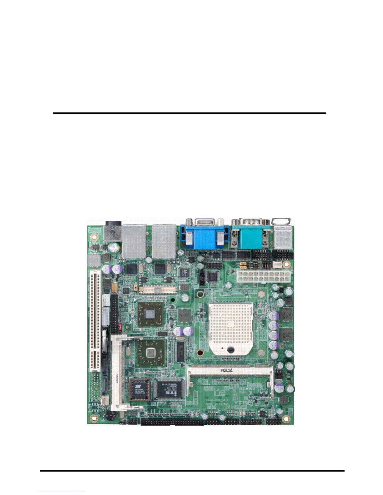
LV-682 User’s Manual
LV-682
Mini-ITX motherboard
User’s Manual
Edition: 1.00
2008/02/01
Page 2

LV-682 User’s Manual 1
Copyright
The trademarks mentioned in the manual are legally registered to their respective
companies.
Disclaimer
Notice
The written content provided with this produc t in the property of Taiwan Commate. No part
of this manual may be reproduced, copied, transmitted in any form or by any means without
prior written permission of Taiwan Commate.
Manual Classification
In order to assist in the use of this product, Taiwan Commate has categorized the user
manual. For detailed product information and specifications, please carefully read the
“ Product User Manual ”.
Trademark
All trademarks are the property of their respective holders.
Any questions please visit our website at TUhttp://www.commell.com.twUT.
Page 3

LV-682 User’s Manual 2
Packing List
Please check package component before you use our products.
☆ LV – 682 board
☆ Quick Installation Guide
☆ CD for manual and drivers
☆ Cable Kit (CPU cooler, IDE cable, Serial ATA cable, Serial Port cable, I/O
Shield, Power cable)
Page 4

LV-682 User’s Manual 3
Table Of Contents
General Information
< Introduction >…..……….………………………………………………………………5
< Specification>.................................................................... 錯誤! 尚未定義書籤。
< Block Diagram>...................................................................................................9
<Mechanical Drawing >..........................................................................................9
Hardware Installation
<Connector Location>..........................................................................................12
< List of Connectors >………………………………………………………………….13
<Jumper Locations>.............................................................................................14
< List of Jumpers>………………………………………………………………………14
< Jumpers Setting>……………………………………………………………………..15
< LVDS Panel Volt age Selection ( JP1 ) >……………………………………………15
< Clear CMOS Selection ( JU5 ) >…………………………………………………….15
<COM2 RS232/422/485 Slection ( JP3, JP2 )>……………………………………..16
<LVDS Connector ( CN2 )>……………………………………………………………17
< VGA & AUDIO Connector ( CN5 )>…………………………………………………17
< GPIO Connector ( CN6 ) >…………………………………………………………..18
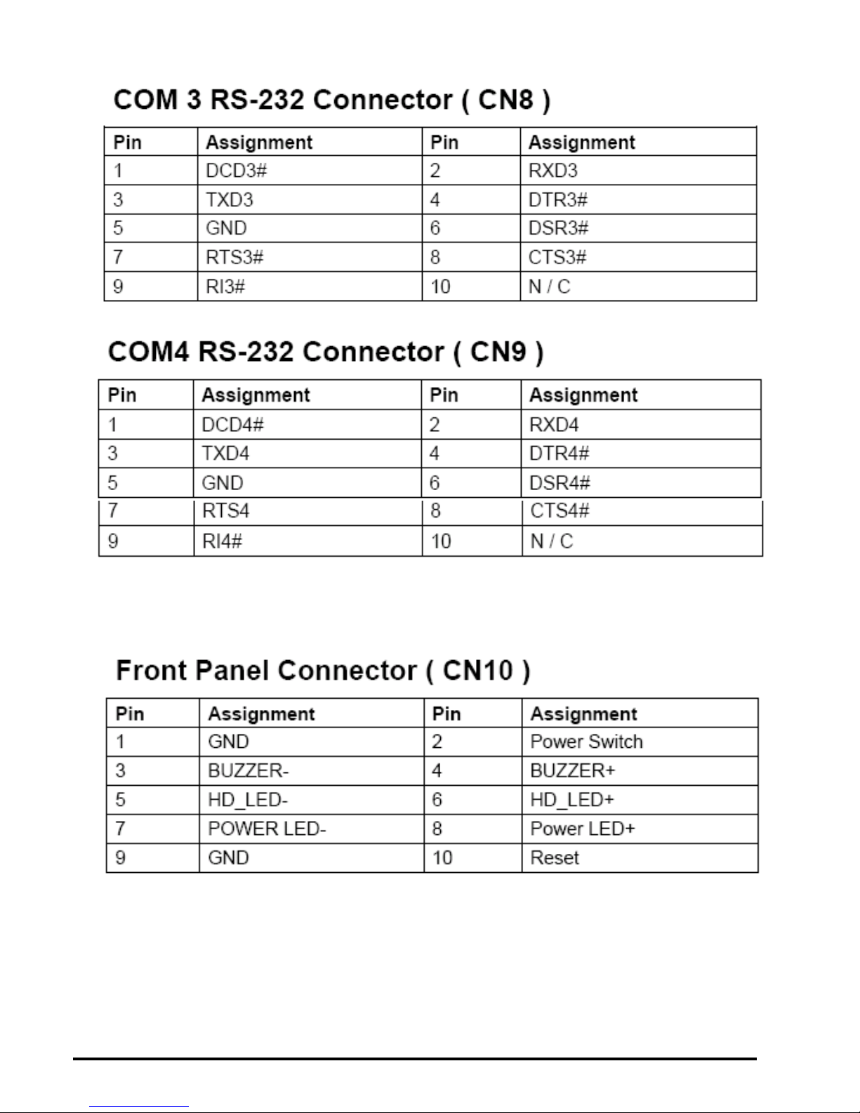
< COM3 RS-232 Connector ( CN8 ) >………………………………………………..18
< COM4 RS-232 Connector ( CN9 )>………………………………………………...18
< Front Panel Connector ( CN10 ) >………………………………………………….19
< EIDE Connector Connector ( J4 ) >………………………………………………...19
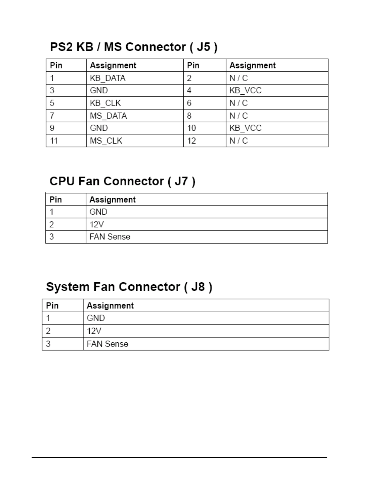
< PS2 KB/ MS Connector ( J5 ) >……………………………………………………..20
< CPU Fan Connector ( J7 ) >…………………………………………………………20
< Systen Fan Connector ( J8 ) >………………………………………………………20
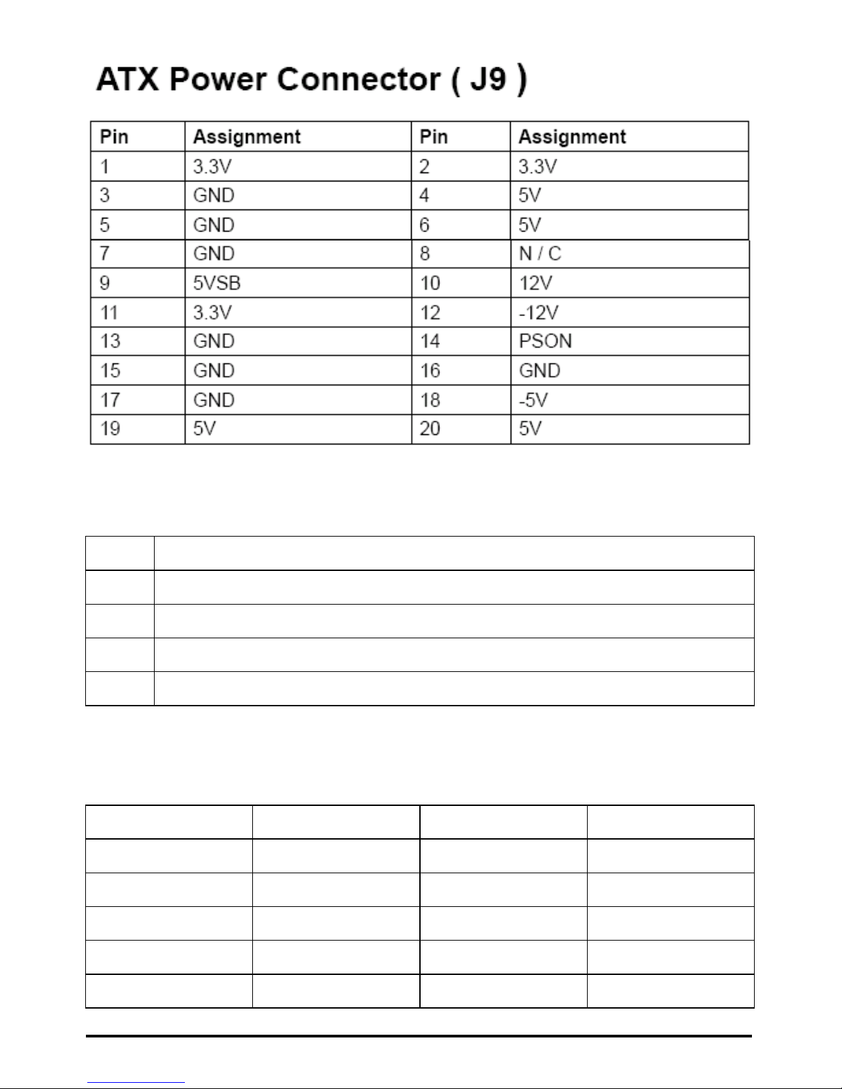
< ATX Power Connector ( J9 ) >……………………………………………………….20
< Slim Floppy Connector ( J11 ) >…………………………………………………….21
< COM1 RS-232 Connector ( COM1 Down ) >………………………………………22
< COM1 RS-232 Connector ( COM1 Up )>…………………………………………..22
Page 5

LV-682 User’s Manual 4
< USB1 Connector ( USB1 ) >…………………………………………………………22
< USB2 Connector ( USB2 ) >………………………………………………………...22
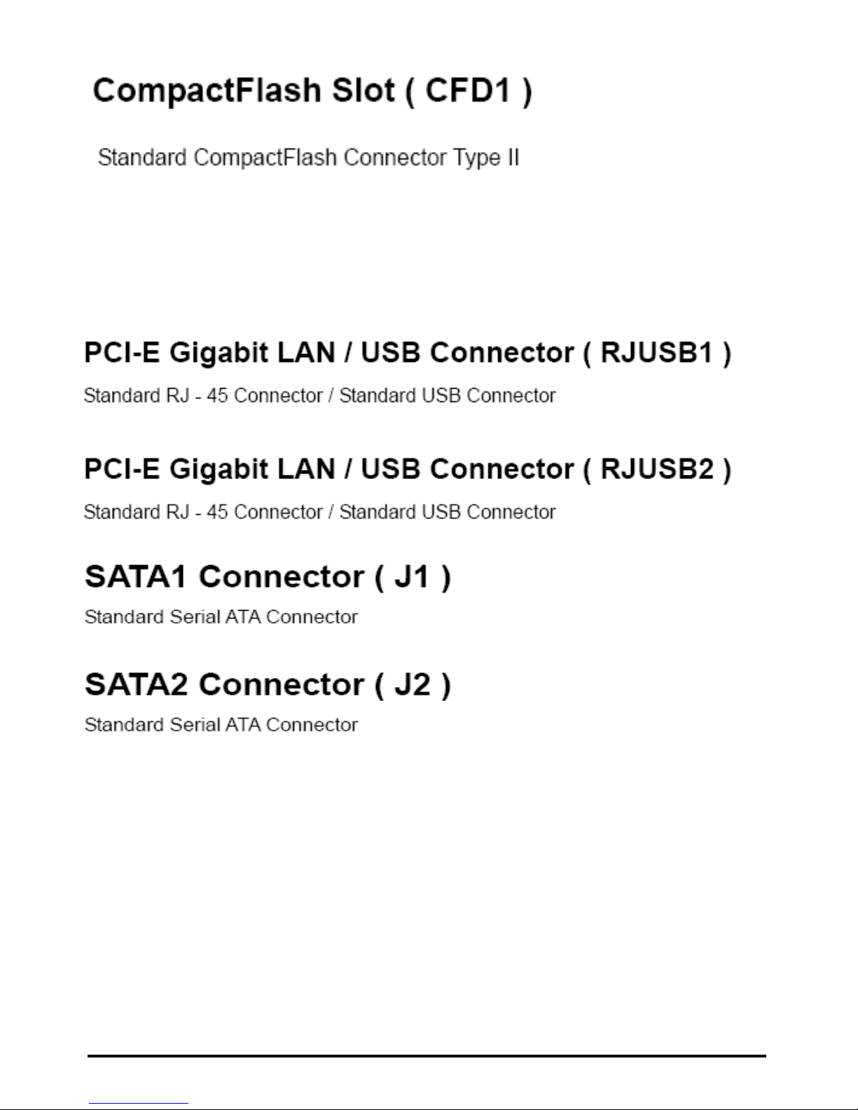
< CompactFlash Slot ( CFD1 ) >………………………………………………………22
< SoDIMM Slot ( DIMMA1 ) >………………………………………………………….22
< SoDIMM Slot ( DIMMA2 ) >………………………………………………………….23
< Mini - PCI Slot ( MPCI1 ) >…………………………………………………………...23
<PCI-E Gigabit LAN / USB Connector ( RJUSB1 A / B )>…………………………23
<PCI-E Gigabit LAN / USB Connector ( RJUSB1 A / B ) >…………………………23
<SATA1 Connector ( SATA1 ) >…………………………….…………………………23
<SATA2 Connector ( SATA2 ) >…………………………….…………………………23
BIOS Setup
<AwardBIOS CMOS Setup Utilit>…………………………………………………….24
<Main CMOS Features>………………………………………………………………24
<Advanced BIOS Feature>……………………………………………………………26
<Power Management Setup>…………………………………………………………27
<PnP / PCI Configurations>…………………………………………………………..28
<Peripherials Setup>…………………………………………………………………..29
<PC Health Status>……………………..……………………………………………..31
<Boot Status>…………………………………………………………………………..32
<Save & Exit Setup>…………………………………………………………………..33
<Load Optimized Defaults>…………………………………………………………..33
<Exit Without Saving>…….…………………………………………………………..33
<Set Password>…………..…………………………………………………………...33
Appendix
<Watch Dog timer Setting > ............................................34
Page 6

LV-682 User’s Manual 5
General Information
Introduction
The LV-682 Mini – ITX board incorporates the AT I RS690E + AT I RS600chipset, supports
the AMD Turion 64 / Sampron uPGA 638 Pin processors with 800 MHz Front Side Bus
(FSB), The RS690E integrates an ATI RADEON X-1250-based 2D/3D graphics engine,
dual display, The SB600 is a south bridge that integrates key I/O, communications, and
audio features. The board supports DDRII 667MHz system memory, PCI interface, PCI-E
Gigabit LAN, Audio, LVDS, DVI Compact Flash, Mini – PCI, Serial ATA, USB 2.0, COM,
IEEE 1394.
Multimedia Applications
For multimedia application solution, ATI RS690E chipset provides on board high
performance graphics, 24 – bit LVDS interface, DVI and Audio function. This feature will be
good of use in very requirement of the multimedia application.
Widely Expanded Interface
The board provides PCI slot, you can add a third LAN port, and also provides Mini – PCI slot
and Compact Flash Type II slot.
Page 7

LV-682 User’s Manual Introduction
Product Specification
6
Specification
Board LV-682 Mini - ITX
CPU AMD Mobile Turion 64x2 638-pin Processor
Sempron 638-pin Processor
Chipset AMD RS690E + SB600
Memory 2 DDR II SoDIMM slot support DDR II 533 / 667 MHz SDRAM Up
to 4GB
VGA Built in AMD RS690E chipset
I / O Control AMD SB600 + ITE 8712 + Fintek F81216D
LAN 2 Realtek RTL8111B 10 / 100 / 1000Mbit
PCI-Express Giga LAN
Audio AMD SB600 with Realtek ALC655 Codec
IDE 1 44Pin UDMA 33 connection
SATA 2 Serial ATA II 3.0 Gbit/sec ports
Slot 1 Mini – PCI slot
1 CompactFlash slot
1 PCI slot
BIOS AMI 4Mb PnP Flash
GPIO 16 – bit digital I / O
Green Function ACPI 1.0 and APM 1.2 compliant
Watchdog Timer System reset programmable watchdog timer with 1 ~ 255 sec. of
time - out
H / W Monitoring ITE 8712 support power supply voltage and temperature
monitoring functions
Real Time Clock AMD SB600 built – in RTC with Lithium battery
Form Factor Mini – ITX 6.69 “( L ) x 6.69” ( W ) / 17 x 17 mm
Page 8

LV-682 User’s Manual
7
VGA Display
Chipset AMD RS690E chipset
Memory Shared system memory up to 256M
Display CRT / LCD monitor with analog for 24 – bit LVDS interface
DVI Support DVI display
Internal I/O Ports
GPIO 1 GPIO Port Connector
USB 2 USB Connector Supports 4 USB ports
Serial Port 2 RS-232 Connector, COM3 with 5V power COM4
with 12V power
CDIN 1 CDIN Connector
Audio 1 Audio Connector
IEEE1394 1 IEEE 1394 Connector
IDE 1 44-Pin IDE Connector
LVDS 1 24-Bit LVDS Connector
Inverter 1 LCD Inverter Connector
DVI 1 DVI
FAN 2 FAN Connector
External I/O Ports
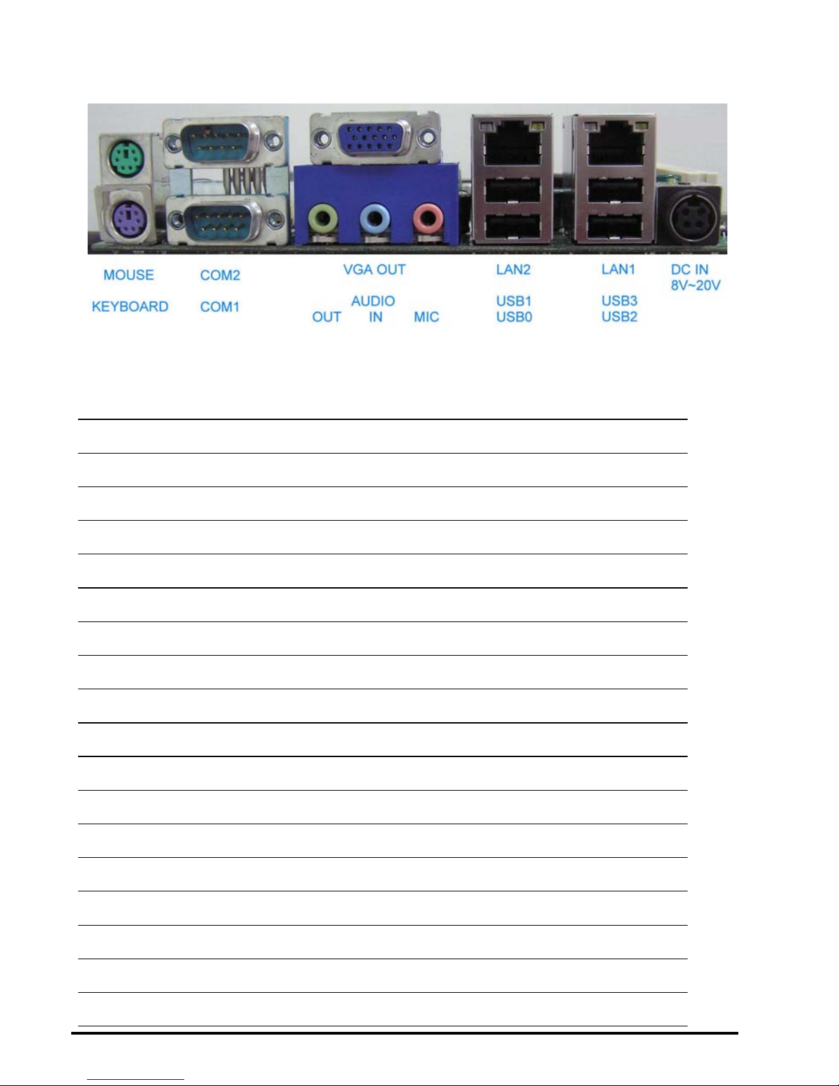
Keyboard/ Mouse 1 PS / 2 ports
Serial Ports 1 external RS–232 port ( COM 1 ) with 5V power
1 external RS–232 / 422 / 485 port ( COM 2 ) with 12V power
VGA 1 VGA port
Audio 1 external jack for MIC – In / Line – In / Line – Out
LAN 2 external RJ – 45 ports with LED
USB 4 external USB 2.0 ports
Page 9

LV-682 User’s Manual
8
Power And Environment
POWER ATX 20-Pin power connector OR 8~21V full range 4 –Pins
DC adapter
TEMPERATURE Operating temperature with 0°C~60°C (32°F~140°F)
Storage temperature with 20°C~80°C (-68°F~176°F)
Page 10
LV-682 User’s Manual
9
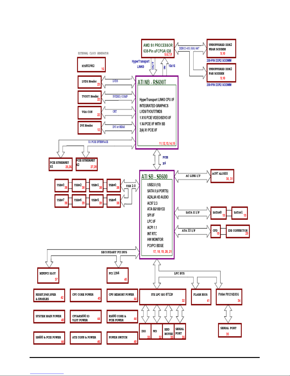
1.3 <Block Diagram>
Page 11
LV-682 User’s Manual
10
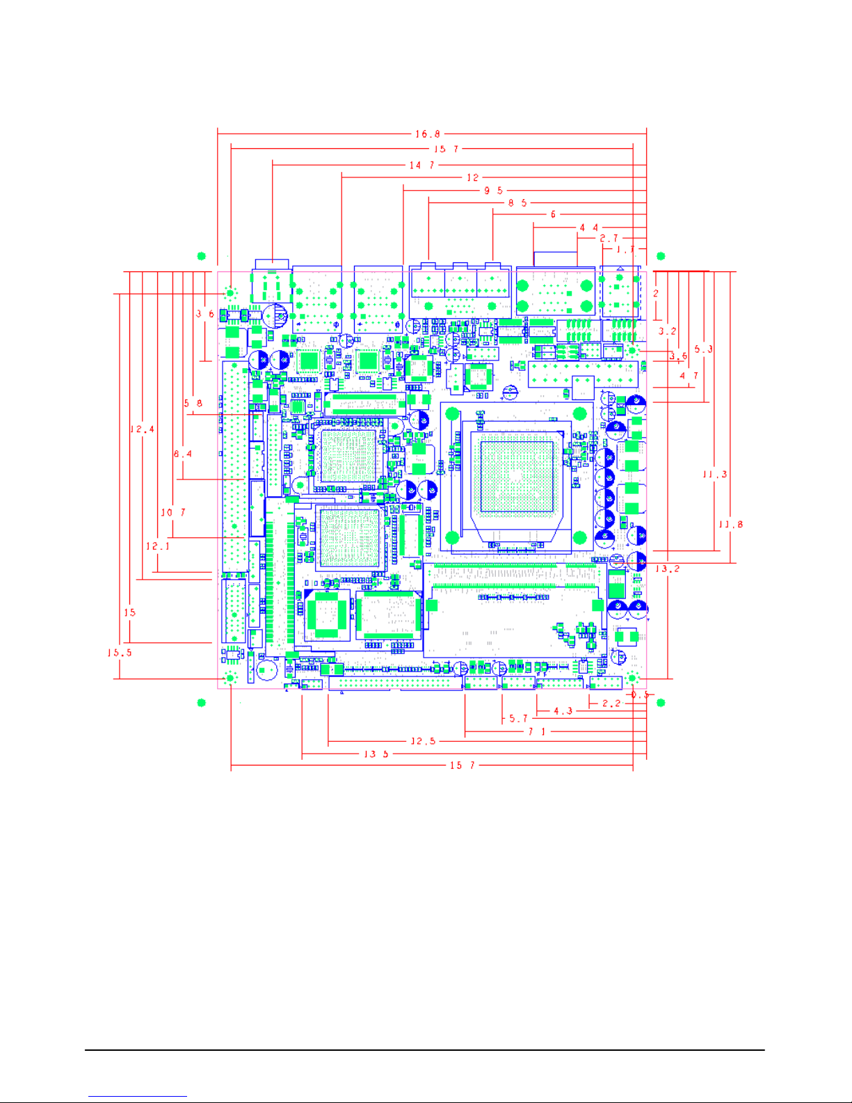
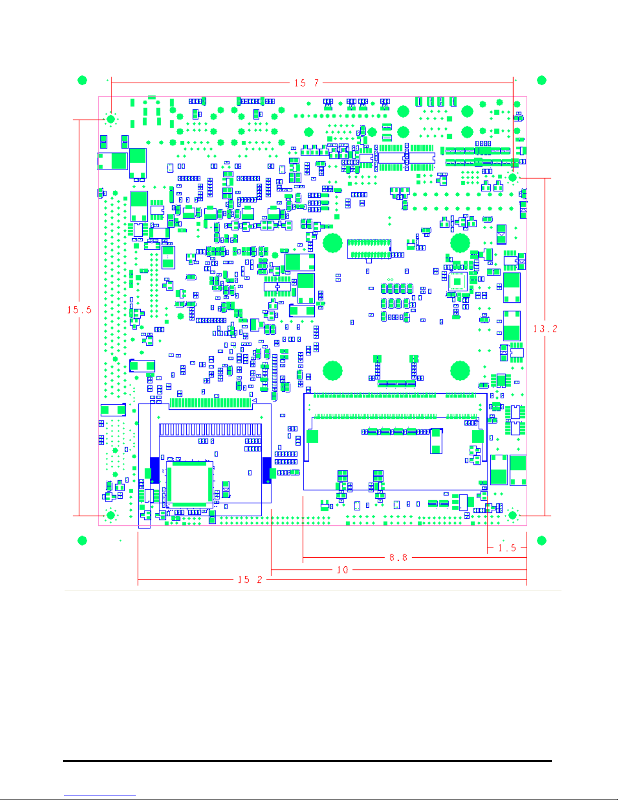
1.4 <Mechanical Drawing >
Page 12
LV-682 User’s Manual
11
Solder Side
Page 13
LV-682 User’s Manual
12
Component Side
Page 14
LV-682 User’s Manual
13
Solder Side
Page 15
LV-682 User’s Manual
14
I / O Panel
Connectors
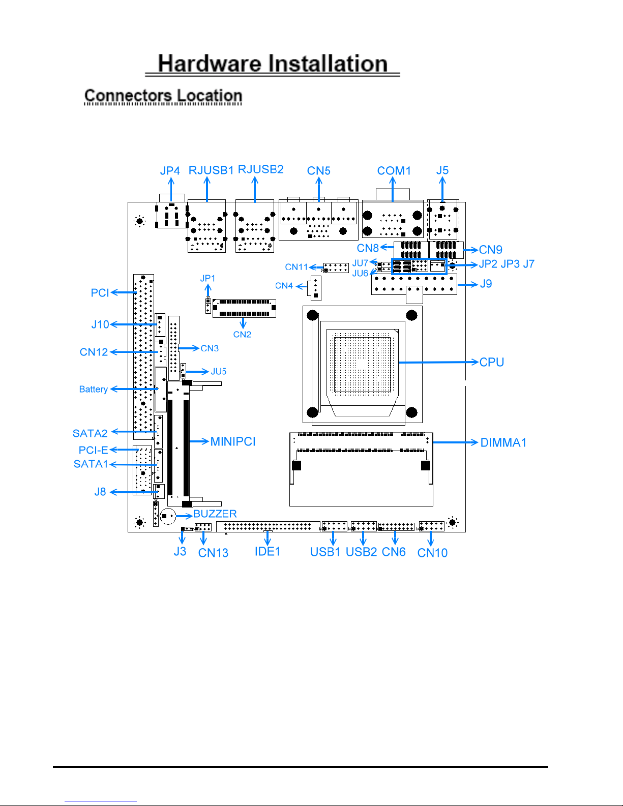
Connector Function
CN2 LVDS Connector
CN3 DVI
CN4 CD-IN Connector
CN5 VGA & AUDIO Connector
CN6 GPIO Connector
CN8 COM3 RS-232 Connector
CN9 COM4 RS-232 Connector
CN10 Front Panel Connector
CN11 Front audio Connector
CN12 LVDS Inverter Power Connector
CN13 1394 Connector
J1 SATA1 Connector
J2 SATA2 Connector
J5 PS2 Keyboard / Mouse Connector
J7 CPU Fan Connector
J8 System Fan Connector
J9 ATX Power Connector
Page 16

LV-682 User’s Manual
15
J10 4 Pin Power Connector
12V limited 0.8A Output
5V limited 1A Output
J11 PCI Slot
JP4 DC Power Jack Connector
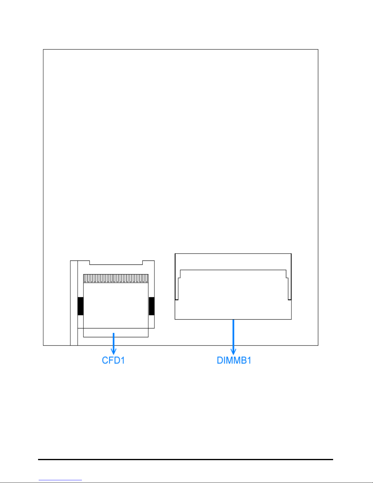
CFD1 CompactFlash Socket
COM1 Down COM1 RS-232 Connector
COM1 Up COM2 RS-232 / RS-422 / RS-485 Connector
DIMMA1 SoDIMM Slot
DIMMB1 SoDIMM Slot
IDE1 44pin IDE Connector
MPCI1 Mini - PCI Slot
RJUSB1 A / B PCI-E Gigabit LAN / USB Connector
RJUSB2 A / B PCI-E Gigabit LAN / USB Connector
USB1 USB1 Connector
USB2 USB2 Connector
Page 17
LV-682 User’s Manual
16
Jumpers Locations
Page 18

LV-682 User’s Manual
17
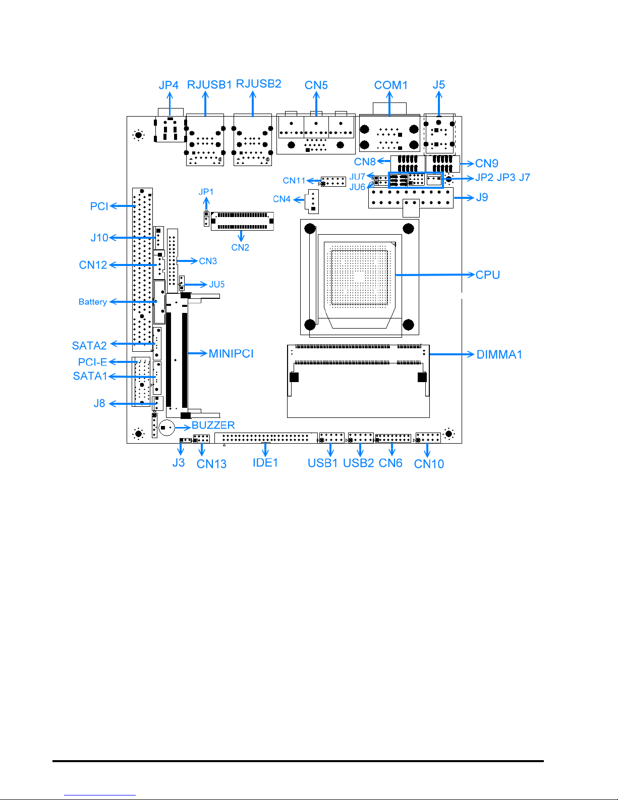
List of Jumpers
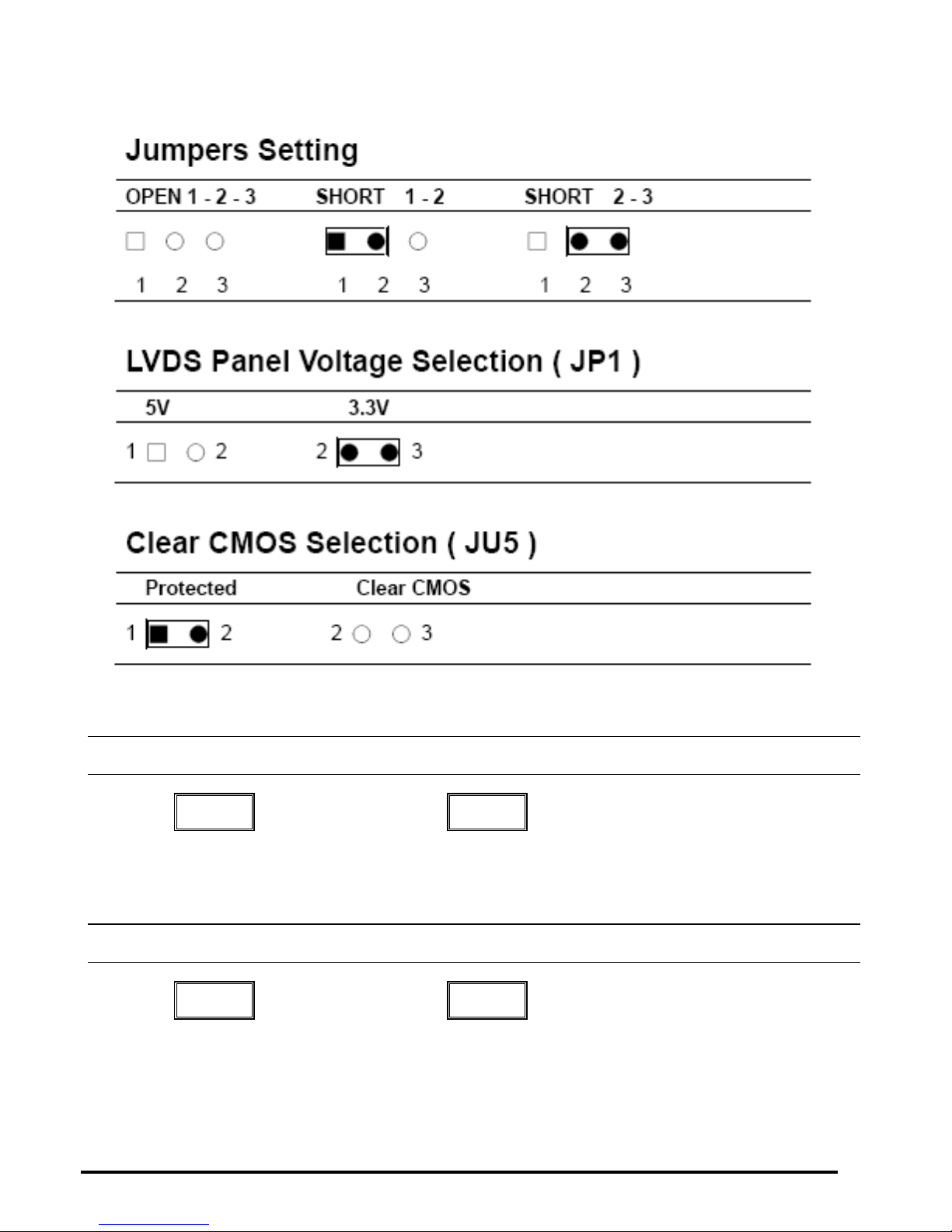
J3 CF card Master / Slave
JP1 LVDS Panel Voltage Selection (+5V / + 3.3V )
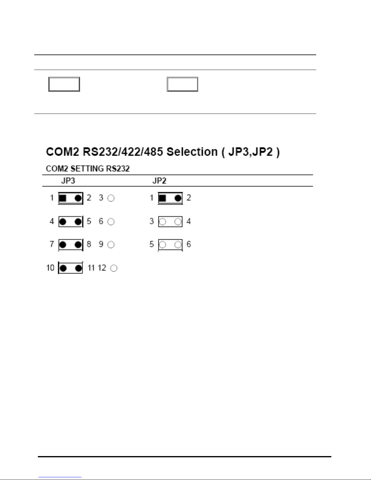
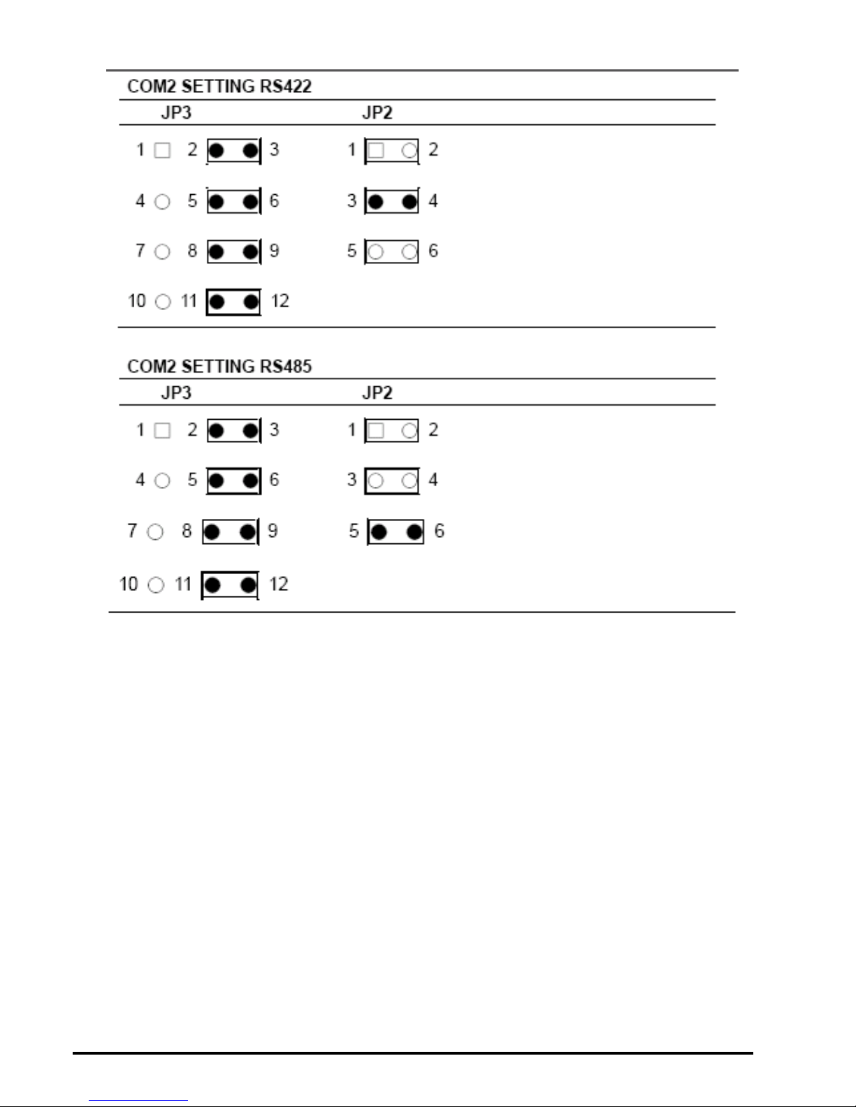
JP2 COM2 RS232/422/485 Select
JP3 COM2 RS232/422/485 Select
JU5 Clear CMOS Selection
JU6 COM2 12V Voltage Select
JU7 COM1 5V Voltage Select
Page 19
LV-682 User’s Manual
18
COM2 Pin 9 Selection ( JU6 )
Ring 12V
■ ● ■ ●
COM1 Pin 9 Selection ( JU7 )
Ring 5V
■ ● ■ ●
1 2 2 3
1 2 2 3
Page 20
LV-682 User’s Manual
19
CF Card Master/Slave Selection ( J3 )
Master Slave
■ ● ○ □ ● ●
1 2 3 1 2 3
Page 21
LV-682 User’s Manual
20
Page 22
LV-682 User’s Manual
21
DC Power Jack Connector ( JP4 )
Pin Assignment Pin Assignment
1 +12V 2 GND
3 GND 4 N/C
5 ENABLK
LVDS Connector ( CN2 )
Pin Assignment Pin Assignment
1 VCC 2 VCC
3 GND 4 GND
5 TXU0N 6 TXLON
7 TXU0P 8 TXL0P
9 GND 10 GND
11 TXU1N 12 TXL1N
13 TXU1P 14 TXL1P
15 GND 16 GND
17 TXU2N 18 TXL2N
19 TXU2P 20 TXL2P
21 GND 22 GND
23 TXU3N 24 TXLCKN
25 TXU3P 26 TXLCKP
27 GND 28 GND
29 TXUCKN 30 TXL3N
31 TXUCKP 32 TXL3P
33 GND 34 GND
35 N/C 36 I2C_CLK
37 N/C 38 I2C_DATA
Page 23

LV-682 User’s Manual
22
39 N/C 40 N/C
DVI Connector ( CN3 )
Pin Assignment Pin Assignment
1 TX1P 2 TX1N
3 GND 4 GND
5 TXCP 6 TXCN
7 GND 8 PVDD
9 N/C 10 N/C
11 TX2P 12 TX2N
13 GND 14 GND
15 TX0P 16 TX0N
17 N/C 18 HPD
19 SDA 20 SCL
21 GND 22 N/C
23 N/C 24 N/C
25 N/C 26 N/C
Page 24
LV-682 User’s Manual
23
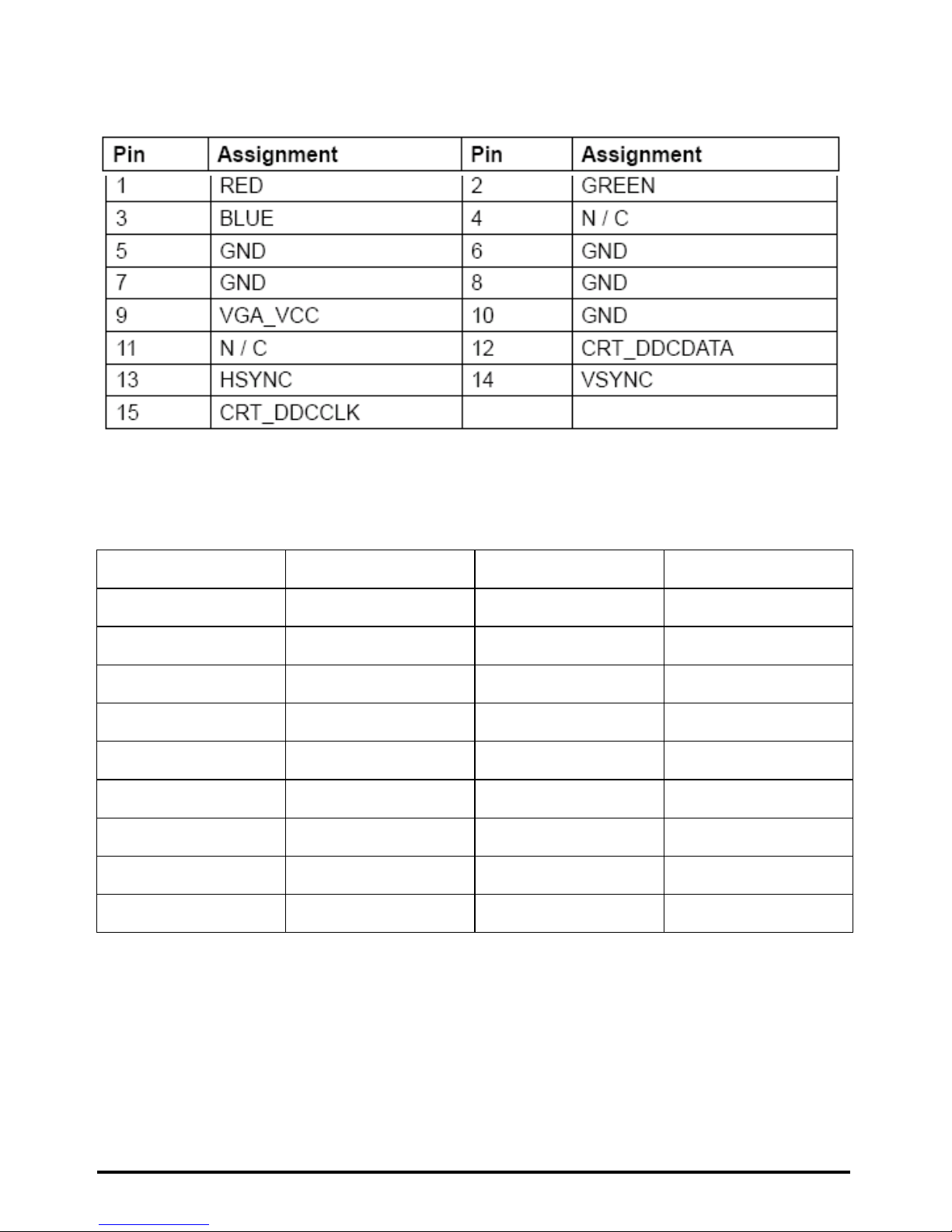
VGA Display Connector ( CN5 )
GPIO Connector ( CN6 )
Pin Assignment Pin Assignment
1
GPIO1-2 2 GPIO1-1
3 GPIO1-4 4 GPIO1-3
5 GPIO1-6 6 GPIO1-5
7 GPIO1-8 8 GPIO1-7
9 GPIO1-10 10 GPIO1-9
11 GPIO1-12 12 GPIO1-11
13 GPIO1-14 14 GPIO1-13
15 GPIO1-16 16 GPIO1-15
17 GND 18 +5V
Page 25
LV-682 User’s Manual
24
Page 26
LV-682 User’s Manual
25
Front Audio Connector ( CN11 )
Pin Assignment Pin Assignment
1 Front-R 2 Front-L
3 Surround-R 4 Surround-L
5 LFEOUT 6 CENOUT
7 SPDIFO-N 8 SPDIFI-N
9 GND 10 GND
LVDS Inverter Power Connector ( CN12 )
Pin Assignment Pin Assignment
1 +12V 2 GND
3 LVDS_BLON 4 CPIS_BLEN
5 +5V
IEEE 1394 Connector ( CN13 )
Pin Assignment Pin Assignment
1 PWR 2 GND
3 TPB0- 4 TPB0+
5 TPA0- 6 TPA0+
7 GND 8 N/C
Page 27
LV-682 User’s Manual
26
Page 28
LV-682 User’s Manual
27
4 Pin Power Connector ( J10 )
Pin Assignment
1 12V( Yellow ) Limited 0.8A Output
2 GND
3 GND
4 5V ( Red ) Limited 1A Output
COM1 RS-232 Connector (COM1 DOWN)
Pin Assignment Pin Assignment
1 DCD1# 2 RXD1
3 TXD1 4 DTR1#
5 GND 6 CSR1#
7 RTS1# 8 CTS1#
9 RI1#
Page 29

LV-682 User’s Manual
28
COM2 RS-232/422/485 Connector (COM1 UP)
Pin Assignment Pin Assignment
1 DCD2#(422TXD-/485DATA-) 2 RXD2(422RXD+)
3 TXD2(422TXD+/485DATA+) 4 DTR2#(422RXD-)
5 GND 6 DSR2#
7 RTS2# 8 CTS2#
9 RI2#
USB Connector (USB1, USB2)
Pin Assignment Pin Assignment
1 USB_VCC 2 GND
3 USB4- 4 GND
5 USB4+ 6 USB5+
7 GND 8 USB59 GND 10 USB_VCC
Page 30
LV-682 User’s Manual
29
Mini-PCI Slot (MPCI1)
Standard Mini-PCI Connector
CD-IN Connector ( CN4 )
Standard CD-IN Connector
EIDE Connector ( J4 )
Standard 44-pin EIDE Connector
PCI Connector ( J11 )
Standard 120-pin PCI Slot Connector
Page 31
LV-682 User’s Manual
30
BIOS Setup
BIOS SETUP UTILITY
Main Advanced PCIPnP Boot Security Chipset Power
Exit
System Overview
AMIBIOS
Version :08.00.14
Build Date :06/14/07
ID :08.00.14
Processor
AMD Turion ™ 64x2 Mobile Technology TL-56
Speed :1800MHz
Count :2
System Memory
size :1984MB
System Time [ 14:20:34 ]
System Date [ Sat
06/16/2007 ]
Use [ENTER], [TAB]
or [SHIFT-TAB] to
Select a field.
Use [+] or [-] to
Configure system
Time.
← Select
Screen
↑↓ Select Item
+- Change Field
Tab Select Field
F1 General Help
F10 Save and
Exit
ESC Exit
Time
Hour 00 to 23
Minute 00 to 59
Second 00 to 59
Page 32

LV-682 User’s Manual
31
Date
Day Sun to Sat
Month Jan. through Dec.
Date 1 to 31
Year 1999 through 2099
BIOS SETUP UTILITY
Main Advanced PCIPnP Boot Security Chipset
Power Exit
Advanced Settings
CPU Configuration
IDE Configuration
SuperIO Configuration
Hardware Health Configuration
ACPI Configuration
USB Configuration
Option for CPU
← Select Screen
↑↓ Select Item
Tab Select Field
F1 General Help
F10 Save and Exit
ESC Exit
Page 33

LV-682 User’s Manual
32
BIOS SETUP UTILITY
Main Advanced PCIPnP Boot Security Chipset Power
Exit
CPU Configuration
Gart Error Reporting [ Disabled ]
Microcode Update [ Enabled ]
SVM uCode Option [ Enabled ]
Runtime Legacy PSB [ Disabled ]
ACPI 2.0 Objects [ Enabled ]
Maximum Frequency during Post [ Enabled ]
← Select Screen
↑↓ Select Item
+- Change Field
F1 General Help
F10 Save and Exit
ESC Exit
CPU Configuration This items show the CPU information,
BIOS version
of your system ( read only ).
Page 34

LV-682 User’s Manual
33
BIOS SETUP UTILITY
Main Advanced PCIPnP Boot Security Chipset Power
Exit
IDE Configuration
OnBoard PCI IDE Controller [ Primary ]
Primary IDE Master [ Not Detected ]
Primary IDE Slave [ Not Detected ]
Hard Disk write Protect [ Disabled ]
IDE Detext Time Out (sec) [ 35 ]
ATA(PI) 80pin cable Detection
[ Host&Device ]
← Select Screen
↑↓ Select Item
+- Change Field
F1 General Help
F10 Save and Exit
ESC Exit
Primary Master / Slave Enables only the primary IDE
controller.
Hard Disk Write Protect This will be effective only if device is
accessed
through BIOS.
IDE Detext Time Out (sec) Select the time out value for detecting
ATA/ATAPI devices.
ATA(PI) 80pin cable Detection Select the mechanism for detecting
80pin
ATA(PI) cable.
Page 35

LV-682 User’s Manual
34
BIOS SETUP UTILITY
Main Advanced PCIPnP Boot Security Chipset Power
Exit
Configure ITE8712 Super IO Chipset
Serial Port1 Address [ 3F8/IRQ4 ]
Serial Port1 Mode [ Normal ]
Serial Port2 Address [ 2F8/IRQ3 ]
Serial Port2 Mode [ Normal ]
Serial Port3 Address [ 3E8 ]
Serial Port3 IRQ [11 ]
Serial Port4 Address [ 2E8 ]
Serial Port4 IRQ [ 10 ]
← Select Screen
↑↓ Select Item
+- Change Field
F1 General Help
F10 Save and Exit
ESC Exit
Serial Port1 Address
Allows BIOS to select serial port1
base
address.
Serial Port1 Mode Allows BIOS to select mode for serial
port1.
Serial Port2 Address Allows BIOS to select serial port2
base
address.
Serial Port2 Mode Allows BIOS to select mode for serial
port2.
Serial Port3 Address Allows BIOS to select serial port3
base
address.
Serial Port3 Mode Allows BIOS to select serial port3
IRQ.
Page 36

LV-682 User’s Manual
35
Serial Port4 Address Allows BIOS to select serial port4
base
address.
Serial Port4 Mode Allows BIOS to select serial port4
IRQ.
Page 37

LV-682 User’s Manual
36
BIOS SETUP UTILITY
Main Advanced PCIPnP Boot Security Chipset Power
Exit
Hardware Health Configuration
Hardware health Function [ Enabled ]
Temperature Sensor #1 [ Enabled ]
Temperature Sensor #1 [ Enabled ]
Fan1 speed [ Enabled ]
Fan2 speed [ Enabled ]
Hardware health Function [ Enabled ]
Enables hardware
Health Monitoring
Device.
← Select Screen
↑↓ Select Item
+- Change Field
F1 General Help
F10 Save and Exit
ESC Exit
PC Health This option allows you to see the
temperature
Monitoring function feature of the
board. The
Values are read-only as monitored by
the
system and show the PC health
status.
Page 38
LV-682 User’s Manual
37
BIOS SETUP UTILITY
Main Advanced PCIPnP Boot Security Chipset Power
Exit
ACPI Settings
General ACPI Configuration
Advanced ACPI Configuration
← Select Screen
↑↓ Select Item
+- Change Field
F1 General Help
F10 Save and Exit
ESC Exit
BIOS SETUP UTILITY
Main Advanced PCIPnP Boot Security Chipset Power
Exit
General ACPI Configuration
Suspend mode [ Auto ]
Repost video on S3 Resume [ No ]
C1E Support [ Disabled ]
General ACPI
Configuration settings.
← Select Screen
↑↓ Select Item
+- Change Field
F1 General Help
F10 Save and Exit
ESC Exit
Page 39
LV-682 User’s Manual
38
Suspend mode Select the ACPI state used for
system suspend.
Repost video on S3 Resume Determines whether in voke VGA BIOS
post on
S3/STR resume.
BIOS SETUP UTILITY
Main Advanced PCIPnP Boot Security Chipset Power
Exit
Advanced ACPI Configuration
ACPI Version Features [ ACPI V1.0 ]
ACPI APIC Support [ Enabled ]
AMI OEMB [ Enabled ]
Headless Mode [ Disabled ]
← Select Screen
↑↓ Select Item
+- Change Field
F1 General Help
F10 Save and Exit
ESC Exit
ACPI Version Features Enable RSDP points to 64-bit.
ACPI APIC Support Include ACPI APIC t able pointer to RSDT
point lists.
AMI OEMB Include OEMB table pointer to RSDT
point lists.
Page 40

LV-682 User’s Manual
39
Headless Mode Enable/Disable Headless operation
mode through
ACPI.
BIOS SETUP UTILITY
Main Advanced PCIPnP Boot Security Chipset Power
Exit
USB Configuration
Legacy USB support [ Enabled ]
USB 2.0 Controller Mode [ HiSpeed ]
BIOS EHCI Hand-Off [ Enabled ]
← Select Screen
↑↓ Select Item
+- Change Field
F1 General Help
F10 Save and Exit
ESC Exit
Legacy USB support
Enable support for legacy USB. Auto
Option. Disables legacy support if no USB
device are
connected.
USB 2.0 Controller Mode Configures the USB 2.0 controller in
Hispeed(480Mbps) or
fullspeed(12Mbps).
BIOS EHCI Hand-Off This is workaround for OS without
EHCI
hand-off support. The EHCI
ownership chang
should claim by EHCI driver.
Page 41

LV-682 User’s Manual
40
BIOS SETUP UTILITY
Main Advanced PCIPnP Boot Security Chipset
Power Exit
Advanced PCI/PnP Settings
Page 42

LV-682 User’s Manual
41
Clear NVRAM [ No ]
Plug & Play O/S [ No ]
PCI Latency Timer [ 64 ]
Allocate IRQ to PCI VGA [ Yes ]
Palette Snooping [ Disabled ]
PCI IDE BusMaster [ Enabled ]
Off Board PCI/ISA IDE card [ Auto ]
IRQ3 [ Available ]
IRQ4 [ Available ]
IRQ5 [ Available ]
IRQ7 [ Available ]
IRQ9 [ Available ]
IRQ10 [ Available ]
IRQ11 [ Available ]
IRQ14 [ Available ]
IRQ15 [ Available ]
DMA Channel0 [ Available ]
DMA Channel1 [ Available ]
DMA Channel3 [ Available ]
DMA Channel5 [ Available ]
DMA Channel6 [ Available ]
DMA Channel7 [ Available ]
Reserved memory size [ Disabled ]
← Select
Screen
↑↓ Select Item
Tab Select Field
F1 General
Help
F10 Save and
Exit
ESC Exit
Clear NVRAM
Clear NVRAM during system boot.
Plug & Play O/S Lets the BIOS configure all the device
Page 43

LV-682 User’s Manual
42
in the
system
PCI Latency Timer Value in units of PCI clocks for PCI
driver
Latency timer register.
Allocate IRQ to PCI VGA Assigns IRQ to PCI VGA card if card
request IRQ.
Palette Snooping Informs the PCI device on ISA graphics
device is
installed in the system,so the card will
function.
PCI IDE BusMaster BIOS use PCI busmaster for R/W to IDE
device.
Off Board PCI/ISA IDE card Works for most PCI IDE card.
BIOS SETUP UTILITY
Main Advanced PCIPnP Boot Security Chipset
Power Exit
Boot Settings
Page 44
LV-682 User’s Manual
43
Booting Settings Configuration
Boot Device Priority
Removable Drivers
Configure setting during
System boot.
← Select Screen
↑↓ Select Item
Tab Select Field
F1 General Help
F10 Save and Exit
ESC Exit
BIOS SETUP UTILITY
Main Advanced PCIPnP Boot Security Chipset
Power Exit
Boot Settings Configuration
Page 45

LV-682 User’s Manual
44
Quick Boot [ Enabled ]
Quiet Boot [ Disabled ]
Add on Rom Display Mode [ Force
BIOS ]
Bootup Num-lock [ On ]
PS/2 Mouse support [ Auto ]
Interrupt 19 Capture [ Disabled ]
Allows BIOS to Skip
Certain tests while
booting.
This will decrease the
time needed to boot
the system.
← Select Screen
↑↓ Select Item
Tab Select Field
F1 General Help
F10 Save and Exit
ESC Exit
Quick Boot
Allows BIOS to skip certain tests
while booting.
Quiet Boot This will decrease the time needed to
boot the
system. Displays normal POST
message.
Add on Rom Display Mode Set display mode for option ROM.
Bootup Num-lock Select power-on state for numlock
PS/2 Mouse support Select support for PS/2 mouse.
Interrupt 19 Capture Allows option ROMS to trap interrupt 19.
Page 46
LV-682 User’s Manual
45
BIOS SETUP UTILITY
Main Advanced PCIPnP Boot Security Chipset
Power Exit
Security Settings
Change Supervisor Password
Change User Password
Boot sector virus Protection [ Disabled ]
← Select Screen
↑↓ Select Item
Tab Select Field
F1 General Help
F10 Save and Exit
ESC Exit
BIOS SETUP UTILITY
Main Advanced PCIPnP Boot Security Chipset
Power Exit
Chipset configuration
NorthBridge Configuration
SouthBridge Configuration
AMD 690T Configuration
OnBoard Peripheral Configuration
I
← Select Screen
↑↓ Select Item
Tab Select Field
F1 General Help
F10 Save and Exit
ESC Exit
Page 47

LV-682 User’s Manual
46
BIOS SETUP UTILITY
Main Advanced PCIPnP Boot Security Chipset
Power Exit
NorthBridge Chipset configuration
Memory Configuration
Power down control [ Auto ]
I
← Select Screen
↑↓ Select Item
Tab Select Field
F1 General Help
F10 Save and Exit
ESC Exit
Power down control Allows DIMMs to enter power down
mode by
deasserting the clock enable signal
when DIMMs
are not in use.
Page 48
LV-682 User’s Manual
47
BIOS SETUP UTILITY
Main Advanced PCIPnP Boot Security Chipset
Power Exit
Memory Configuration
Memclock Mode [ Auto ]
MCT T iming Mode [ Auto ]
Bank Interleaving [ Auto ]
Enable Clock to all DIMMs [ Disabled ]
Memclk tristate C3/ATLVID [ Disabled ]
DQS Signal Training Control [ Enabled ]
Memory Table remapping [ Enabled ]
← Select Screen
↑↓ Select Item
+- Change Field
F1 General Help
F10 Save and Exit
ESC Exit
Memclock Mode
Select the DRAM frequency
programming
method, if Auto the DRAM speed will
be base
on SPDs.
Bank Interleaving If Auto the memory will be checked
which
executes 64 or 128-bits mode
Enable Clock to all DIMMs Enable Unused clocks to DIMMs even
memory slots
are not populated.
Memclk tristate C3/ATLVID Enable/Disable Memclk Tri-stating during
C3 and
ATLVID.
DQS Signal Training Control Turing this off will require custom
memory timing
programming. Training will be
Page 49

LV-682 User’s Manual
48
automatically disabled
if CS sparing is enable.
Memory Table remapping Enable memory remapping around
memory hole.
BIOS SETUP UTILITY
Main Advanced PCIPnP Boot Security Chipset
Power Exit
SouthBridge Chipset Configuration
AC 97 Audio device [ Enabled ]
USB 1.1 OHCI controllers [ Enabled ]
USB 2.0 EHCI controller [ Enabled ]
OnChip SATA Channel [ Enabled ]
OnChip SATA Type [ Native
IDE ]
BIOS SETUP UTILITY
Main Advanced PCIPnP Boot Security Chipset
Power Exit
AMD 690T Configuration
Internal Graphics Configuration
PCI Express Configuration
Page 50

LV-682 User’s Manual
49
BIOS SETUP UTILITY
Main Advanced PCIPnP Boot Security Chipset
Power Exit
Internal Graphics Configuration
Internal Graphics mode [ UMA ]
UMA Frame buffer size [ 64MB ]
Graphics clock mode [ SYNC ]
GFX engine clock [ 200 ]
Multifunction [ Disabled ]
Primary Video controller
[ PCIE/IGFX/PCI ]
Video Display Devices [ Auto ]
TV standard [ NTSC ]
Expansion mode [ Disabled ]
← Select Screen
↑↓ Select Item
+- Change Field
F1 General Help
F10 Save and Exit
ESC Exit
Page 51

LV-682 User’s Manual
50
BIOS SETUP UTILITY
Main Advanced PCIPnP Boot Security Chipset
Power Exit
Power Configuration
Power Management/APM [ Enabled ]
Suspend Time Out [ Disabled ]
Power Button Mode [ On/Off ]
Video Power Down Mode [ suspend ]
Hard Disk time out(Minute) [ Disabled ]
Restore On AC Power Loss [ Disabled ]
RTC Resume [ Disabled ]
I
Power Management/APM
Enable/Disable SMI based power
management
and APM support.
Suspend Time Out If no activity during this time period the
BIOS will
place the system into suspend low power
state.
are not populated.
Power Button Mode Select Power button functionality.
Page 52

LV-682 User’s Manual
51
BIOS SETUP UTILITY
Main Advanced PCIPnP Boot Security Chipset
Power Exit
Exit Options
Save Changes and Exit
Discard Changes and Exit
Discard changes
Load Optimal Defaults
Load Failsafe Defaults
I
Save Changes and Exit
Exit system setup after saving
changes.
Discard Changes and Exit Exit system setup without saving any
changes.
Discard changes Discard changes done so for to any of
the setup
questions
Load Optimal Defaults Load Optimal default values for all the setup
questions.
Load Failsafe Defaults Load Failsafe default values for all the setup
questions.
Page 53

LV-682 User’s Manual
52
Appendix
Watchdog Timer
User could test watchdog timer function under “ DEBUG.EXE
“ program as follows:
DEBUG Description
O 2e 87
O 2e 01
O 2e 55
O 2e 55
O 2e 07
O 2f 07
O 2e 72
O 2f c0 C0: second ( 40: minute )
O 2e 72
O 2e 73 Control second or minute
O 2f 00 ~ FF O 2f 08 ( 8 second reset )
 Loading...