

Page 1
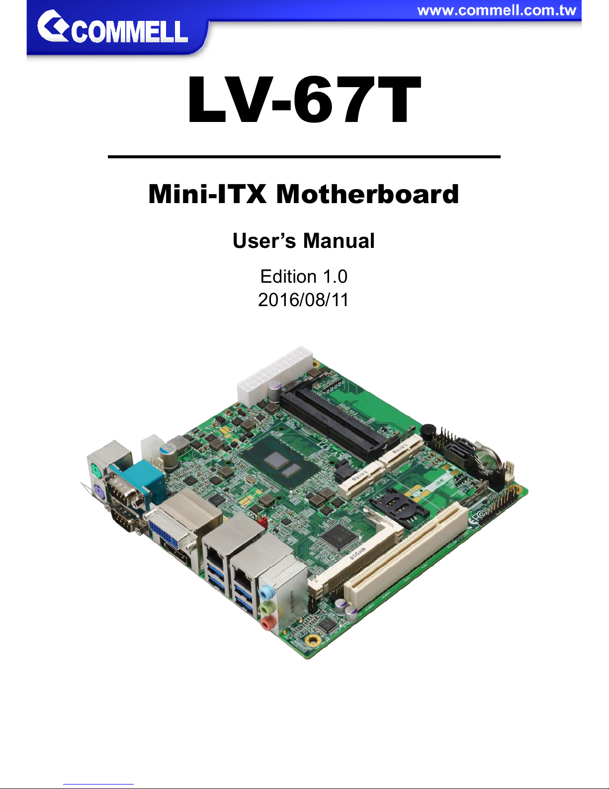
LV-67T
Mini-ITX Motherboard
User’s Manual
Edition 1.0
2016/08/11
Page 2
LV-67T User’s Manual
-1-
Copyright
Copyright 2016, all rights reserved. This document is copyrighted and all rights are reserved.
The information in this document is subject to change without prior notice to make
improvements to the products.
This document contains proprietary information and protected by copyright. No part of this
document may be reproduced, copied, or translated in any form or any means without prior
written permission of the manufacturer.
All trademarks and/or registered trademarks contains in this document are property of their
respective owners.
Disclaimer
The company shall not be liable for any incidental or consequential damages resulting from
the performance or use of this product.
The company does not issue a warranty of any kind, express or implied, including without
limitation implied warranties of merchantability or fitness for a particular purpose.
The company has the right to revise the manual or include changes in the specifications of
the product described within it at any time without notice and without obligation to notify any
person of such revision or changes.
Trademark
All trademarks are the property of their respective holders.
Any questions please visit our website at
TUhttp://www.commell.com.twUT
Page 3
LV-67T User’s Manual
-2-
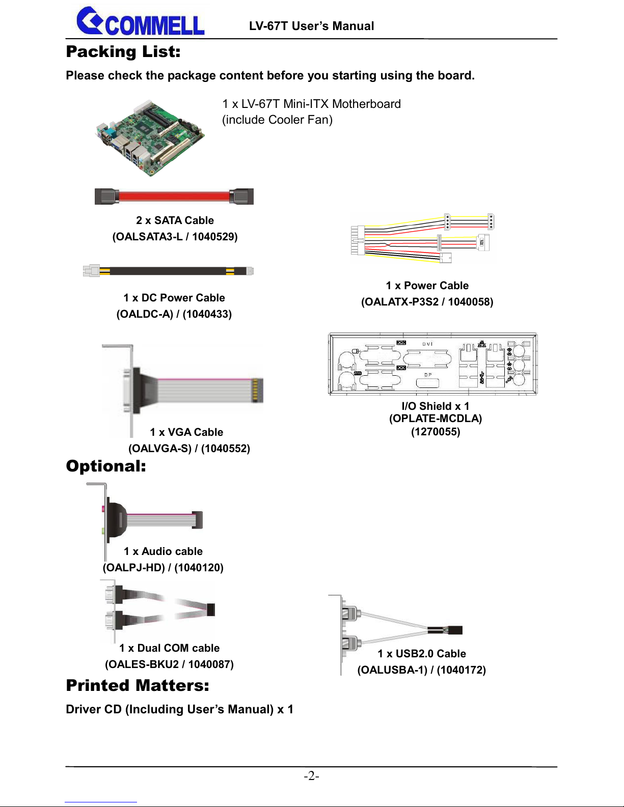
I/O Shield x 1
(OPLATE-MCDLA)
(1270055)
1 x VGA Cable
(OALVGA-S) / (1040552)
Packing List:
Please check the package content before you starting using the board.
Optional:
Printed Matters:
Driver CD (Including User’s Manual) x 1
1 x LV-67T Mini-ITX Motherboard
(include Cooler Fan)
2 x SATA Cable
(OALSATA3-L / 1040529)
1 x Dual COM cable
(OALES-BKU2 / 1040087)
1 x Power Cable
(OALATX-P3S2 / 1040058)
1 x DC Power Cable
(OALDC-A) / (1040433)
1 x Audio cable
(OALPJ-HD) / (1040120)
1 x USB2.0 Cable
(OALUSBA-1) / (1040172)
Page 4

LV-67T User’s Manual
-3-
Index
Chapter 1 <Introduction>............................................................... 4
1.1 <Product Overview> ................................................................................. 4
1.2 <Product Specification> ........................................................................... 5
1.3 <Mechanical Drawing> ............................................................................. 6
1.4 <Block Diagram> ...................................................................................... 9
Chapter 2 <Hardware setup> ....................................................... 10
2.1 <Connector Location and Reference> ................................................... 10
2.1.1 <Internal connectors list> ........................................................... 11
2.1.2 <External connectors list> .......................................................... 11
2.2 <Jumper Location and Reference> ........................................................ 12
2.2.1 <Jumper list> .............................................................................. 12
2.2.2 <Clear CMOS and Power on type selection> ............................ 12
2.3 <Installing the Memory> ......................................................................... 13
2.4 <I/O interface> ........................................................................................ 14
2.4.1 <Serial ATA interface> ................................................................ 14
2.4.2 <Ethernet interface> ................................................................... 14
2.4.3 <Display interface> ..................................................................... 15
2.4.4 <Serial Port interface> ................................................................ 17
2.4.5 <USB interface> ......................................................................... 19
2.4.6 <Audio interface> ....................................................................... 19
2.4.7 <Expansion slot> ........................................................................ 20
2.4.8 <Front panel switch and indicator> ............................................ 21
2.4.9 <Other interface> ........................................................................ 22
2.5 <Power supply>...................................................................................... 24
2.5.1 <Power input> ............................................................................ 24
2.5.2 <Power output> .......................................................................... 25
Appendix A <Flash BIOS> .................................................................................. 26
Appendix B <Win7 Installation Notes> ............................................................. 27
Appendix C <LCD Panel Type select> .............................................................. 28
Appendix D <Programmable GPIO > ................................................................ 29
Appendix E <Programmable Watch Dog Timer> ............................................. 30
Appendix F <SATA RAID function setting> ...................................................... 31
Contact information ............................................................................................ 32
Page 5
LV-67T User’s Manual
-4-
Chapter 1 <Introduction>
1.1 <Product Overview>
LV-67T is Mini-ITX Motherboard which supports 6th Generation Intel® Core™ U-series i7, i5,
i3, Celeron Mobile Processor with Sunrise Point PCH-LP, integrated HD Graphics, DDR4
memory, Realtek High Definition Audio, Intel Gigabit LAN, Serial ATA3 with AHCI function
for a system.
Intel Skylake-U Processor with Sunrise Point PCH-LP
The 6th Generation Intel® Core™ U-series processor family is the next generation,
multi-core mobile processor built on 14 nanometer process with MCP technology.
The Skylake-U has a lower TDP 15W and 28W, it provides new HD Graphics (GT2 and GT3
GPU) support triple display at the same time, maximum supported is up to 32GB of DDR4
and DDR3L, better performance, flexibility and more enhanced security that is suitable for a
variety of intelligent systems the ideal choice.
All in One multimedia solution
The board provides high performance onboard graphics, 24-bit dual channel LVDS interface,
DisplayPort/VGA, DVI, and High Definition Audio, to meet the very requirement of the
multimedia application.
Flexible Expansion Interface
The board provides two MiniPCIe and support mSATA, SIM.
Page 6
LV-67T User’s Manual
-5-
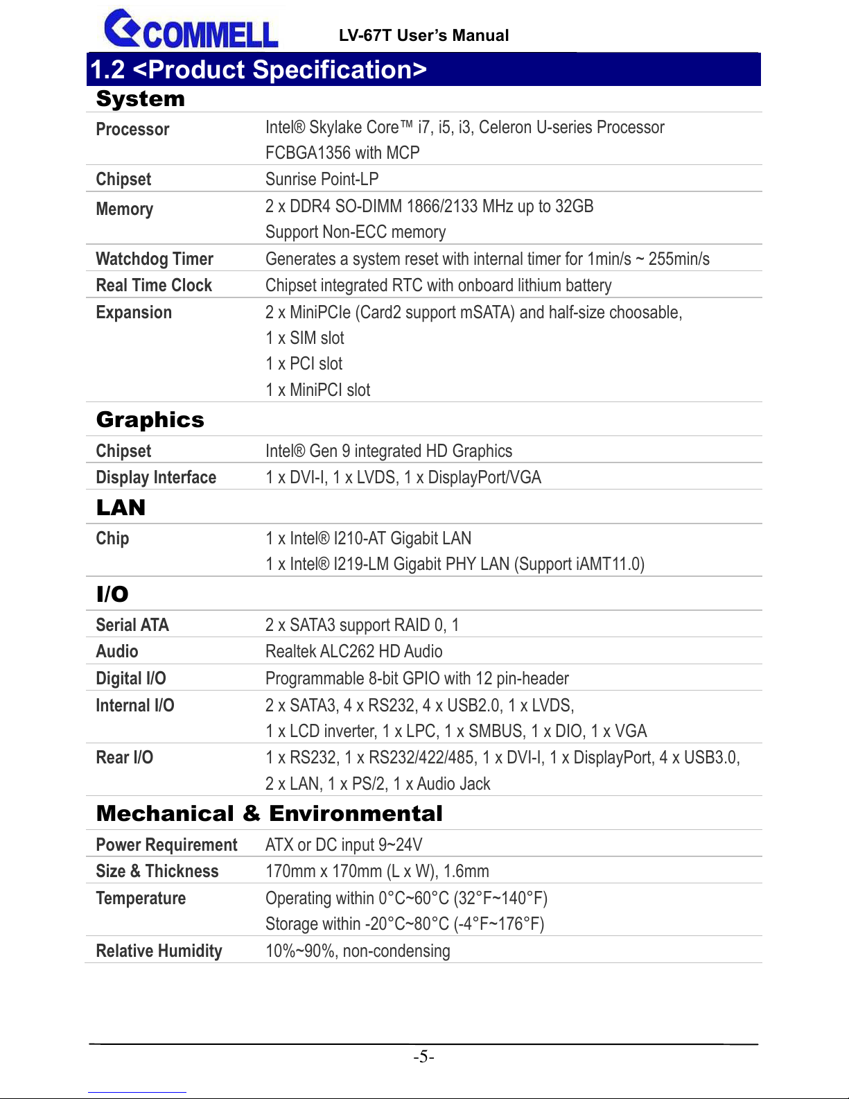
1.2 <Product Specification>
System
Processor
Intel® Skylake Core™ i7, i5, i3, Celeron U-series Processor
FCBGA1356 with MCP
Chipset
Sunrise Point-LP
Memory
2 x DDR4 SO-DIMM 1866/2133 MHz up to 32GB
Support Non-ECC memory
Watchdog Timer
Generates a system reset with internal timer for 1min/s ~ 255min/s
Real Time Clock
Chipset integrated RTC with onboard lithium battery
Expansion
2 x MiniPCIe (Card2 support mSATA) and half-size choosable,
1 x SIM slot
1 x PCI slot
1 x MiniPCI slot
Graphics
Chipset
Intel® Gen 9 integrated HD Graphics
Display Interface
1 x DVI-I, 1 x LVDS, 1 x DisplayPort/VGA
LAN
Chip
1 x Intel® I210-AT Gigabit LAN
1 x Intel® I219-LM Gigabit PHY LAN (Support iAMT11.0)
I/O
Serial ATA
2 x SATA3 support RAID 0, 1
Audio
Realtek ALC262 HD Audio
Digital I/O
Programmable 8-bit GPIO with 12 pin-header
Internal I/O
2 x SATA3, 4 x RS232, 4 x USB2.0, 1 x LVDS,
1 x LCD inverter, 1 x LPC, 1 x SMBUS, 1 x DIO, 1 x VGA
Rear I/O
1 x RS232, 1 x RS232/422/485, 1 x DVI-I, 1 x DisplayPort, 4 x USB3.0,
2 x LAN, 1 x PS/2, 1 x Audio Jack
Mechanical & Environmental
Power Requirement
ATX or DC input 9~24V
Size & Thickness
170mm x 170mm (L x W), 1.6mm
Temperature
Operating within 0°C~60°C (32°F~140°F)
Storage within -20°C~80°C (-4°F~176°F)
Relative Humidity
10%~90%, non-condensing
Page 7

LV-67T User’s Manual
-6-
1.3 <Mechanical Drawing>
Positive
Page 8

LV-67T User’s Manual
-7-
I/O
Page 9
LV-67T User’s Manual
-8-
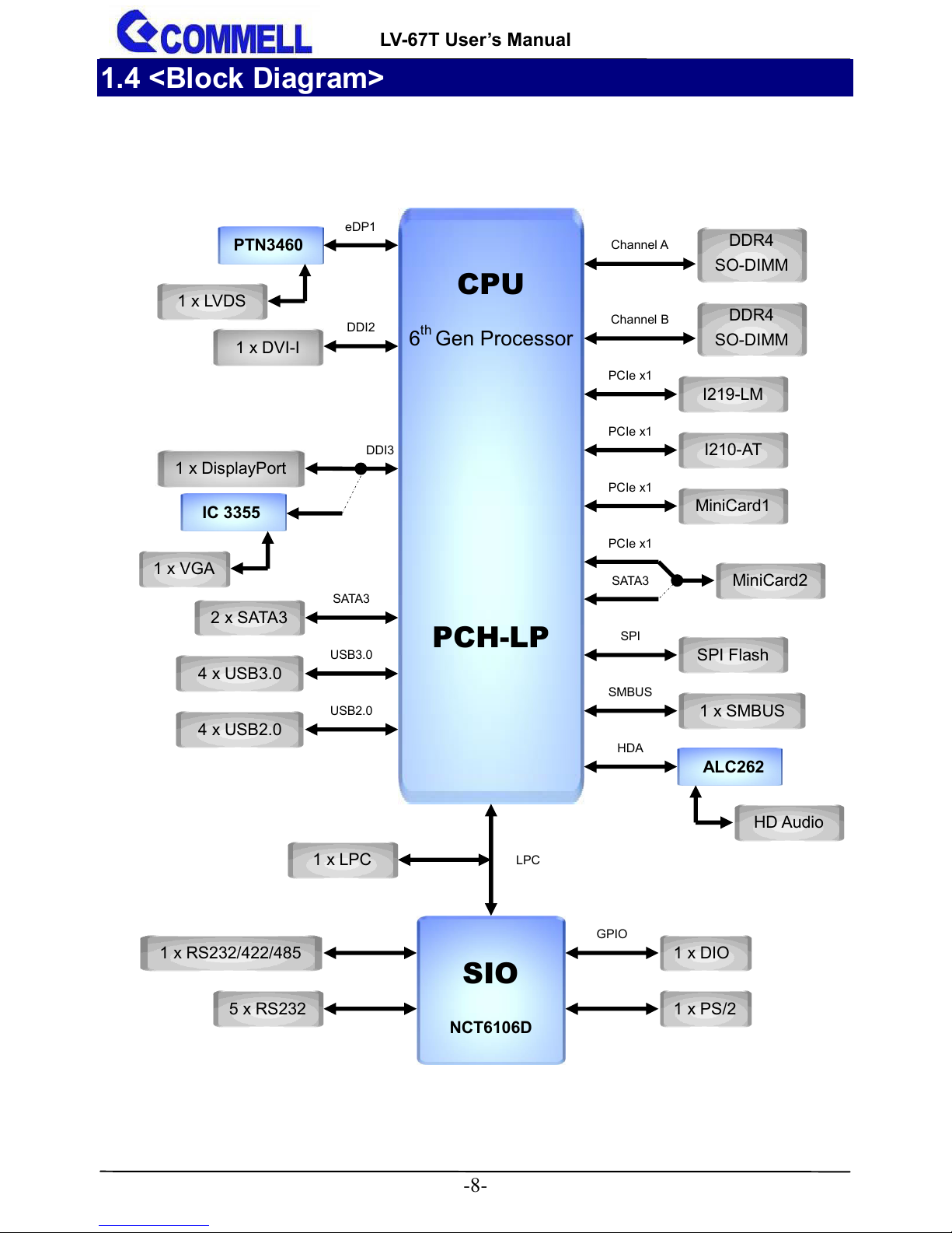
1.4 <Block Diagram>
CPU
6
th
Gen Processor
PCH-LP
DDR4
SO-DIMM
1 x DisplayPort
PTN3460
1 x LVDS
SIO
NCT6106D
DDI3
Channel A
eDP1
2 x SATA3
SATA3
4 x USB3.0
4 x USB2.0
USB3.0
USB2.0
SPI Flash
SPI
PCIe x1
I219-LM
HDA
HD Audio
PCIe x1
SATA3
LPC
1 x LPC
ALC262
5 x RS232
1 x SMBUS
1 x PS/2
I210-AT
PCIe x1
MiniCard1
PCIe x1
MiniCard2
1 x RS232/422/485
1 x DIO
SMBUS
GPIO
DDI2
IC 3355
1 x VGA
1 x DVI-I
DDR4
SO-DIMM
Channel B
Page 10

LV-67T User’s Manual
-9-
Chapter 2 <Hardware setup>
2.1 <Connector Location and Reference>
MINI_CARD1
CN_LPC
CN_AUDIO
CN_INV
CN_USB1
JFRNT
SATA3-2
CN_COM5/6
DC_IN
CPUFAN
CN_SMBUS
MINI_CARD2
CN_COM3/4
CN_DIO
MINIPCI
ATX
SATA3-2
CN_USB2
Audio
LAN1
USB3.0
SIMM
PS2
COM2
COM1
DVI-I
DisplayPort
SYSFAN
CN_LVDS
CN_CRT
PCI
SATA3-1
SO-DIMM1
SO-DIMM2
LAN2
USB3.0
Page 11
LV-67T User’s Manual
-10-
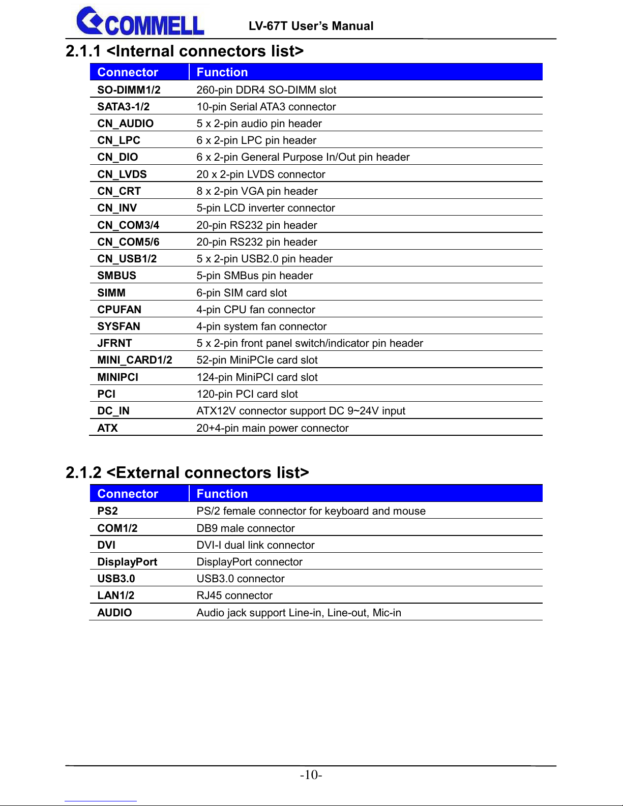
2.1.1 <Internal connectors list>
Connector
Function
SO-DIMM1/2
260-pin DDR4 SO-DIMM slot
SATA3-1/2
10-pin Serial ATA3 connector
CN_AUDIO
5 x 2-pin audio pin header
CN_LPC
6 x 2-pin LPC pin header
CN_DIO
6 x 2-pin General Purpose In/Out pin header
CN_LVDS
20 x 2-pin LVDS connector
CN_CRT
8 x 2-pin VGA pin header
CN_INV
5-pin LCD inverter connector
CN_COM3/4
20-pin RS232 pin header
CN_COM5/6
20-pin RS232 pin header
CN_USB1/2
5 x 2-pin USB2.0 pin header
SMBUS
5-pin SMBus pin header
SIMM
6-pin SIM card slot
CPUFAN
4-pin CPU fan connector
SYSFAN
4-pin system fan connector
JFRNT
5 x 2-pin front panel switch/indicator pin header
MINI_CARD1/2
52-pin MiniPCIe card slot
MINIPCI
124-pin MiniPCI card slot
PCI
120-pin PCI card slot
DC_IN
ATX12V connector support DC 9~24V input
ATX
20+4-pin main power connector
2.1.2 <External connectors list>
Connector
Function
PS2
PS/2 female connector for keyboard and mouse
COM1/2
DB9 male connector
DVI
DVI-I dual link connector
DisplayPort
DisplayPort connector
USB3.0
USB3.0 connector
LAN1/2
RJ45 connector
AUDIO
Audio jack support Line-in, Line-out, Mic-in
Page 12
LV-67T User’s Manual
-11-
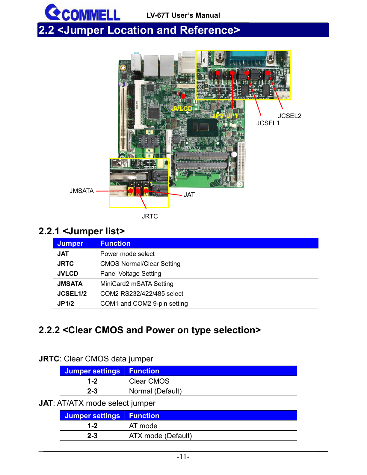
2.2 <Jumper Location and Reference>
2.2.1 <Jumper list>
Jumper
Function
JAT
Power mode select
JRTC
CMOS Normal/Clear Setting
JVLCD
Panel Voltage Setting
JMSATA
MiniCard2 mSATA Setting
JCSEL1/2
COM2 RS232/422/485 select
JP1/2
COM1 and COM2 9-pin setting
2.2.2 <Clear CMOS and Power on type selection>
JRTC: Clear CMOS data jumper
Jumper settings
Function
1-2
Clear CMOS
2-3
Normal (Default)
JAT: AT/ATX mode select jumper
Jumper settings
Function
1-2
AT mode
2-3
ATX mode (Default)
JVLCD
JAT
JRTC
JMSATA
JP2
JP1
JCSEL1
JCSEL2
1
Page 13

LV-67T User’s Manual
-12-
2.3 <Installing the Memory>
In the process, the board must be powered off.
1. Put the memory tilt into the slot. Note the Memory notch key aligned slot key.
2. Then press down till lock into the mounting notch.
3. To remove the memory, push outward on both sides of the latch.
Key
Mounting notch
Press down
Latch
Page 14
LV-67T User’s Manual
-13-
2.4 <I/O interface>
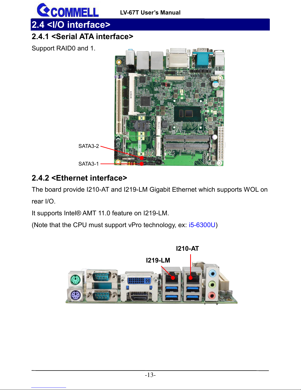
2.4.1 <Serial ATA interface>
Support RAID0 and 1.
2.4.2 <Ethernet interface>
The board provide I210-AT and I219-LM Gigabit Ethernet which supports WOL on
rear I/O.
It supports Intel® AMT 11.0 feature on I219-LM.
(Note that the CPU must support vPro technology, ex:
i5-6300U)
I219-LM
SATA3-1
SATA3-2
I210-AT
Page 15
LV-67T User’s Manual
-14-
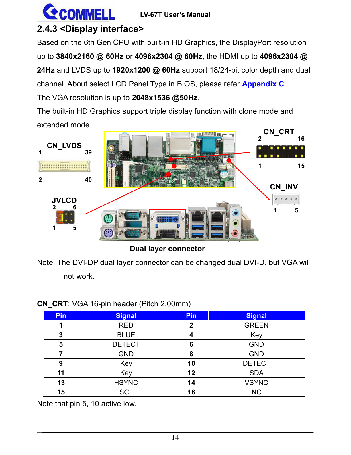
2.4.3 <Display interface>
Based on the 6th Gen CPU with built-in HD Graphics, the DisplayPort resolution
up to 3840x2160 @ 60Hz or 4096x2304 @ 60Hz, the HDMI up to 4096x2304 @
24Hz and LVDS up to 1920x1200 @ 60Hz support 18/24-bit color depth and dual
channel. About select LCD Panel Type in BIOS, please refer
Appendix C.
The VGA resolution is up to 2048x1536 @50Hz.
The built-in HD Graphics support triple display function with clone mode and
extended mode.
Note: The DVI-DP dual layer connector can be changed dual DVI-D, but VGA will
not work.
CN_CRT: VGA 16-pin header (Pitch 2.00mm)
Pin
Signal
Pin
Signal
1
RED
2
GREEN
3
BLUE
4
Key
5
DETECT
6
GND
7
GND
8
GND
9
Key
10
DETECT
11
Key
12
SDA
13
HSYNC
14
VSYNC
15
SCL
16
NC
Note that pin 5, 10 active low.
CN_CRT
CN_LVDS
1
40
JVLCD
2
39
1
15
2
16
5
1
6
2
CN_INV
1
5
Dual layer connector
Page 16

LV-67T User’s Manual
-15-
CN_LVDS: LVDS 40-pin connector (Model: HIROSE DF13-40DP-1.25V compatible)
Pin
Signal
Pin
Signal
2
Set by JVLCD
1
Set by JVLCD
4
Detect (Active low)
3
GND
6
A_LVDS_0-
5
B_LVDS_0-
8
A_LVDS_0+
7
B_LVDS_0+
10
GND
9
GND
12
A_LVDS_1-
11
B_LVDS_1-
14
A_LVDS_1+
13
B_LVDS_1+
16
GND
15
GND
18
A_LVDS_2-
17
B_LVDS_2-
20
A_LVDS_2+
19
B_LVDS_2+
22
GND
21
GND
24
A_LVDS_CLK-
23
B_LVDS_3-
26
A_LVDS_CLK+
25
B_LVDS_3+
28
GND
27
GND
30
A_LVDS_3-
29
B_LVDS_CLK-
32
A_LVDS_3+
31
B_LVDS_CLK+
34
GND
33
GND
36
LVDS_DDCSCL
35
NC
38
LVDS_DDCSDA
37
NC
40
NC
39
NC
Note: Pin4 only need to be connected to GND
CN_INV: LVDS 5-pin Backlight power connector
Pin
Signal
1
12V
2
Backlight Control
3
GND
4
GND
5
Enable Backlight
JVLCD: LVDS panel power select jumper
Jumper settings
Function
1-2
3.3V (Default)
3-4
5V
5-6
12V
Effective patterns of connection: 1-2 / 3-4 / 5-6
Other may cause damage
Page 17
LV-67T User’s Manual
-16-
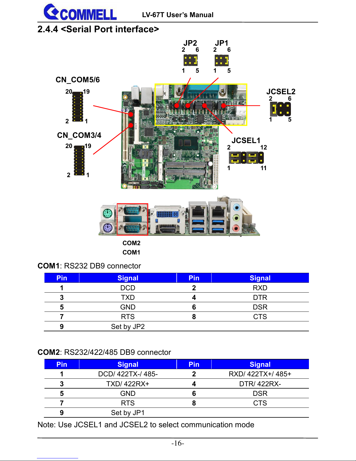
2.4.4 <Serial Port interface>
COM1: RS232 DB9 connector
Pin
Signal
Pin
Signal
1
DCD
2
RXD
3
TXD
4
DTR
5
GND
6
DSR
7
RTS
8
CTS
9
Set by JP2
COM2: RS232/422/485 DB9 connector
Pin
Signal
Pin
Signal
1
DCD/ 422TX-/ 485-
2
RXD/ 422TX+/ 485+
3
TXD/ 422RX+
4
DTR/ 422RX-
5
GND
6
DSR
7
RTS
8
CTS
9
Set by JP1
Note: Use JCSEL1 and JCSEL2 to select communication mode
CN_COM5/6
CN_COM3/4
1
2
19
20
1
2
20
19
2 1 6
5
JP1
JP2
2
6
1
5
JCSEL1
1
2
JCSEL2
2
6
1
5
1
11
12
COM2
COM1
Page 18
LV-67T User’s Manual
-17-
COM3/4,5/6: RS232 20-pin header (Pitch 1.27mm x 2.54mm)
Pin
Signal
Pin
Signal
1
DCD1
2
RXD1
3
TXD1
4
DTR1
5
GND
6
DSR1
7
RTS1
8
CTS1
9
RI1
10
NC
11
DCD2
12
RXD2
13
TXD2
14
DTR2
15
GND
16
DSR2
17
RTS2
18
CTS2
19
RI2
20
Key
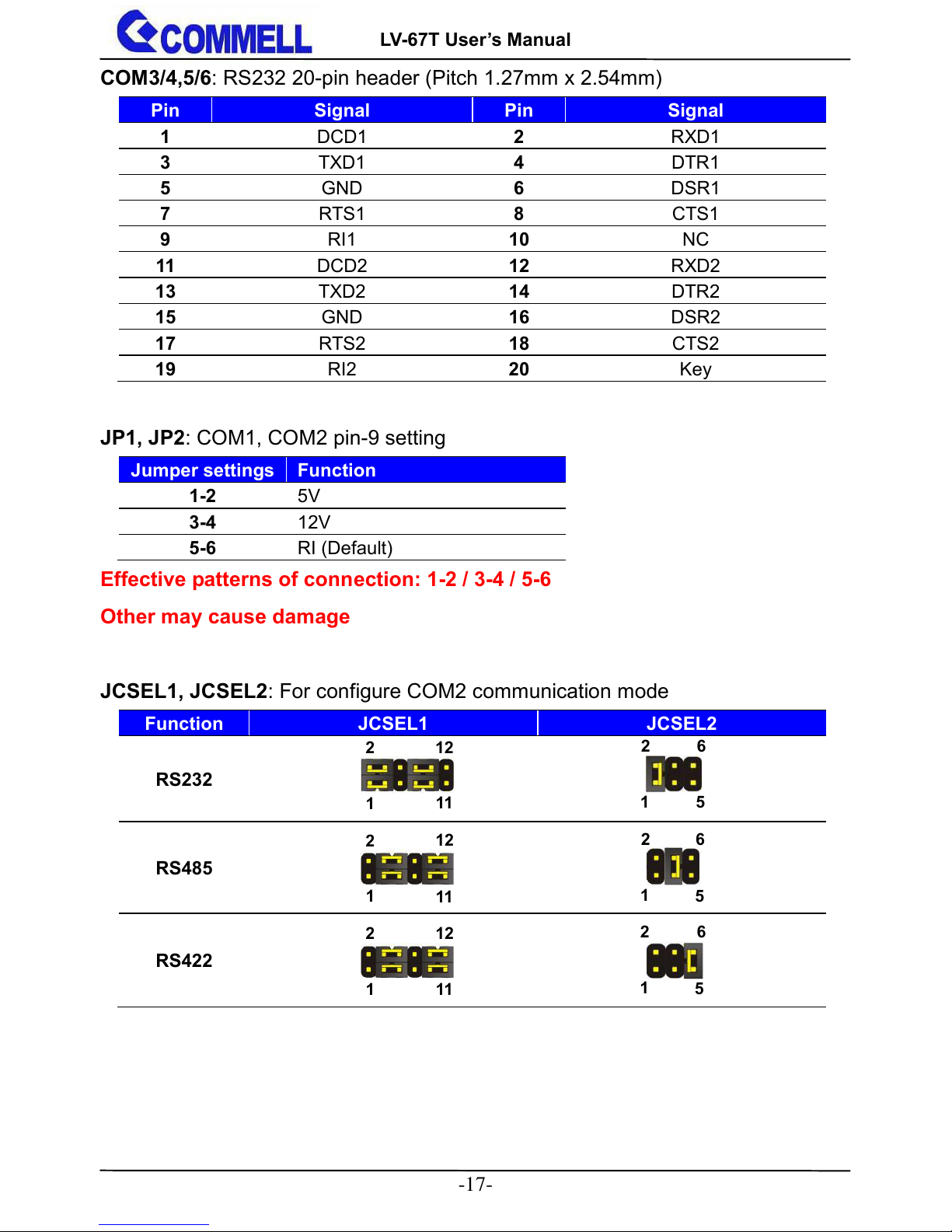
JP1, JP2: COM1, COM2 pin-9 setting
Jumper settings
Function
1-2
5V
3-4
12V
5-6
RI (Default)
Effective patterns of connection: 1-2 / 3-4 / 5-6
Other may cause damage
JCSEL1, JCSEL2: For configure COM2 communication mode
Function
JCSEL1
JCSEL2
RS232
RS485
RS422
1
12
1
12
1
12
6
1
5
1
5
1
2
11
2
11
2
11
2
2
2 5 6
6
Page 19

LV-67T User’s Manual
-18-
2.4.5 <USB interface>
USB1 & 2 are USB3.0 interface.
CN_USB1/2: Front panel USB2.0 10-pin header (Pitch 2.54mm)
Pin
Signal
Pin
Signal
1
5VSB
2
5VSB
3
DATA0-
4
DATA1-
5
DATA0+
6
DATA1+
7
GND
8
GND
9
GND
10
Key
2.4.6 <Audio interface>
CN_AUDIO
1
10
CN_USB2
1
10 2 2
9
USB3.0-1
9
CN_USB1
1 2 9
10
USB2
USB3.0-2
(5VSB)
(5VSB)
Rear Audio Jack
Line in
Line out
Mic in
Page 20
LV-67T User’s Manual
-19-
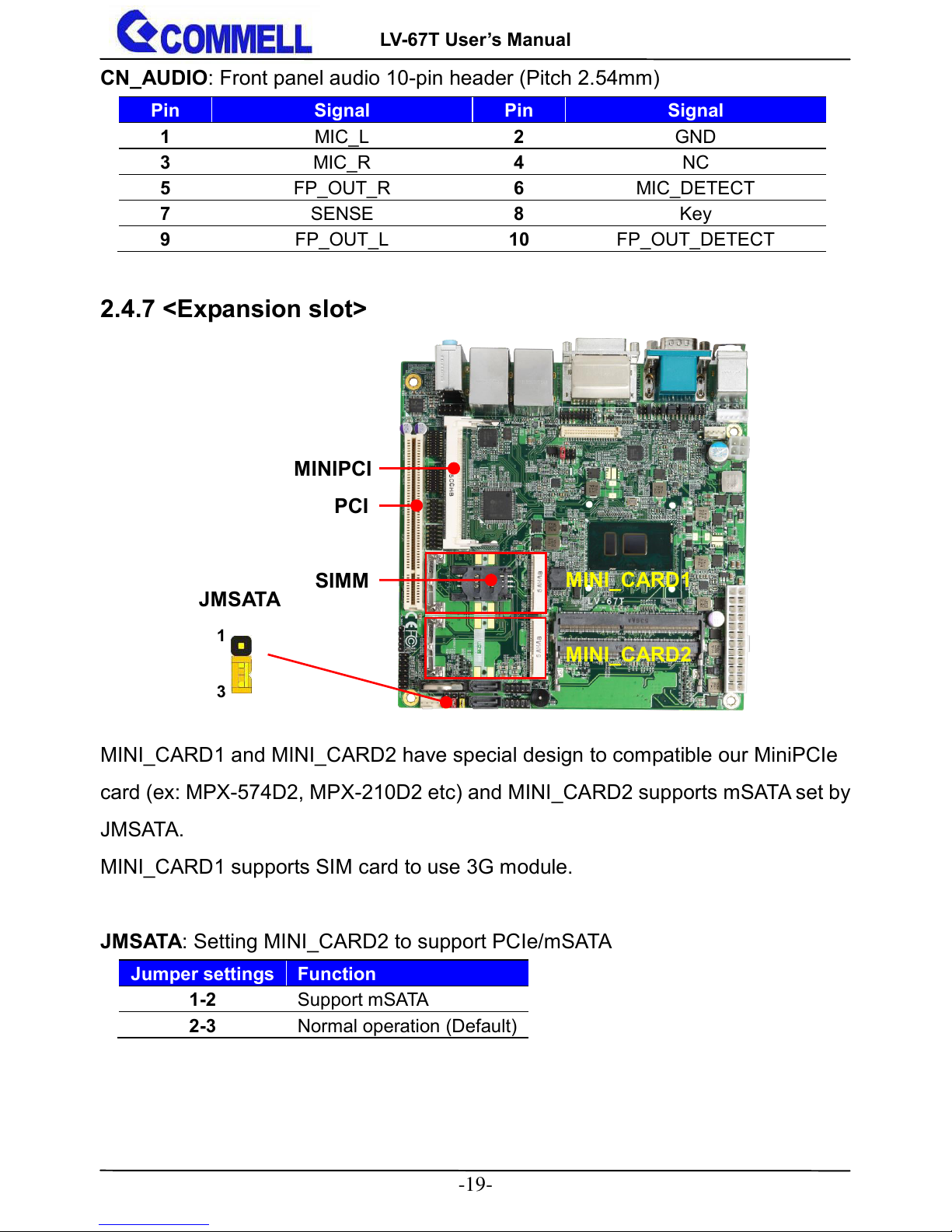
CN_AUDIO: Front panel audio 10-pin header (Pitch 2.54mm)
Pin
Signal
Pin
Signal
1
MIC_L
2
GND
3
MIC_R
4
NC
5
FP_OUT_R
6
MIC_DETECT
7
SENSE
8
Key
9
FP_OUT_L
10
FP_OUT_DETECT
2.4.7 <Expansion slot>
MINI_CARD1 and MINI_CARD2 have special design to compatible our MiniPCIe
card (ex: MPX-574D2, MPX-210D2 etc) and MINI_CARD2 supports mSATA set by
JMSATA.
MINI_CARD1 supports SIM card to use 3G module.
JMSATA: Setting MINI_CARD2 to support PCIe/mSATA
Jumper settings
Function
1-2
Support mSATA
2-3
Normal operation (Default)
MINI_CARD2
JMSATA
MINI_CARD1
1
3
SIMM
PCI
MINIPCI
Page 21

LV-67T User’s Manual
-20-
<SIM>
This is for 3G miniPCIe card which doesn’t have SIM slot.
2.4.8 <Front panel switch and indicator>
Slide the direction of the arrow open the cover.
Insert the SIM card and make
sure the direction is correct
Then press down and slide the
direction of the arrow close the cover.
JFRNT
1
14 2 13
Page 22
LV-67T User’s Manual
-21-
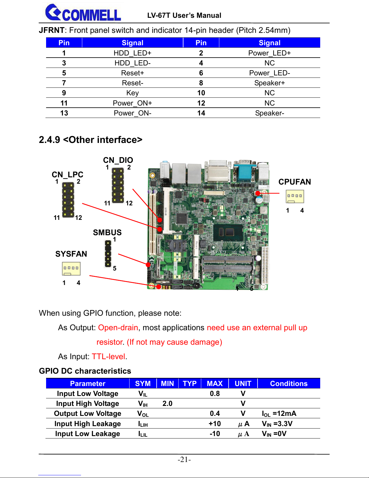
JFRNT: Front panel switch and indicator 14-pin header (Pitch 2.54mm)
Pin
Signal
Pin
Signal
1
HDD_LED+
2
Power_LED+
3
HDD_LED-
4
NC
5
Reset+
6
Power_LED-
7
Reset-
8
Speaker+
9
Key
10
NC
11
Power_ON+
12
NC
13
Power_ON-
14
Speaker-
2.4.9 <Other interface>
When using GPIO function, please note:
As Output:
Open-drain, most applications need use an external pull up
resistor. (If not may cause damage)
As Input: TTL-level.
GPIO DC characteristics
Parameter
SYM
MIN
TYP
MAX
UNIT
Conditions
Input Low Voltage
VIL
0.8
V
Input High Voltage
VIH
2.0 V
Output Low Voltage
VOL
0.4
V
IOL =12mA
Input High Leakage
I
LIH
+10
μA
VIN =3.3V
Input Low Leakage
I
LIL
-10
μA
VIN =0V
CN_DIO
1
12 2 11
CN_LPC
1
11
12
2
SMBUS
1
5
CPUFAN
1
4
SYSFAN
1
4
1
5
Page 23

LV-67T User’s Manual
-22-
CN_DIO: GPIO 12-pin header (Pitch 2.00mm)
Pin
Signal
Pin
Signal
1
GND
2
GND
3
GPIO0
4
GPIO4
5
GPIO1
6
GPIO5
7
GPIO2
8
GPIO6
9
GPIO3
10
GPIO7
11
5V
12
12V
CN_LPC: LPC 12-pin header (Pitch 2.00mm)
Pin
Signal
Pin
Signal
1
CLK
2
RST
3
-LFRAME
4
LAD3
5
LAD2
6
LAD1
7
LAD0
8
3.3V
9
SERIRQ
10
GND
11
3.3VSB
12
NC
Note: Support TPM module.
SMBUS: SMBus 5-pin connector
Pin
Signal
1
5V
2
NC
3
SMBDAT
4
SMBCLK
5
GND
CPUFAN: CPU cooler fan 4-pin connector
Pin 1 2 3 4
Signal
GND
12V
Sensor
Control
SYSFAN: System cooler fan 4-pin connector
Pin 1 2 3 4
Signal
GND
12V
Sensor
Control
Page 24

LV-67T User’s Manual
-23-
2.5 <Power supply>
2.5.1 <Power input>
The DC_IN support 9~24V wide voltage input.
Note that the DC_IN and ATX do not use at the same time, it will certainly
cause damage.
DC_IN: ATX12V 4-pin connector
Pin
Signal
Pin
Signal
1
GND
2
GND
3
9~24V
4
9~24V
ATX: main power 24-pin connector (As input)
Pin
Signal
Pin
Signal
1
3.3V
13
3.3V
2
3.3V
14
NC
3
GND
15
GND
4
5V
16
-PSON
5
GND
17
GND
6
5V
18
GND
7
GND
19
GND
8
Power_OK
20
NC
9
5VSB
21
5V
10
12V
22
5V
11
12V
23
5V
12
3.3V
24
GND
DC_IN
1
4
3
2
ATX
1
24
13
12
Page 25
LV-67T User’s Manual
-24-
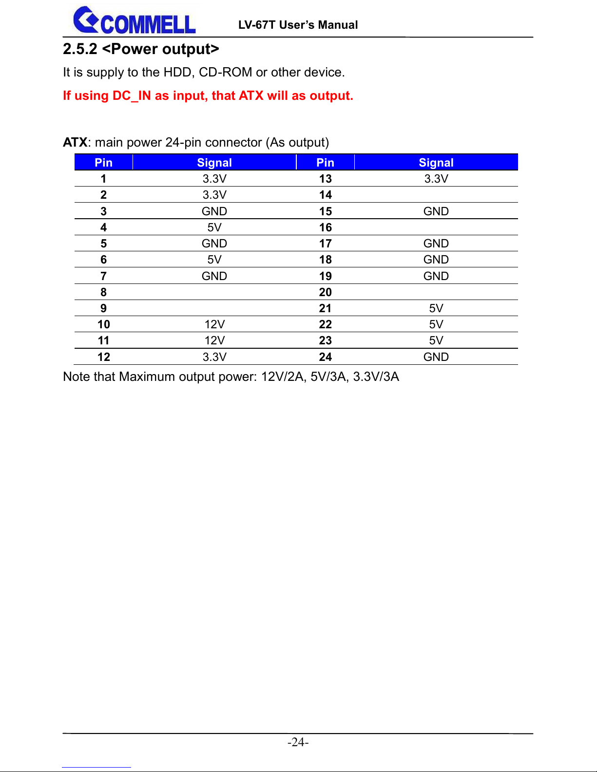
2.5.2 <Power output>
It is supply to the HDD, CD-ROM or other device.
If using DC_IN as input, that ATX will as output.
ATX: main power 24-pin connector (As output)
Pin
Signal
Pin
Signal
1
3.3V
13
3.3V
2
3.3V
14
3
GND
15
GND
4
5V
16
5
GND
17
GND
6
5V
18
GND
7
GND
19
GND
8 20
9 21
5V
10
12V
22
5V
11
12V
23
5V
12
3.3V
24
GND
Note that Maximum output power: 12V/2A, 5V/3A, 3.3V/3A
Page 26

LV-67T User’s Manual
-25-
Appendix A <Flash BIOS>
A.1 <Flash tool>
The board is based on Phoenix BIOS and can be updated easily by the BIOS
auto flash tool. You can download the tool online at the address below:
LV-67T reflash tool
The tool’s file name is “fpt.exe”, it’s the utility that can write the data into the
BIOS flash chip and update the BIOS.
A.2 <Flash BIOS process>
1. Please make a bootable UFD which can boot into DOS enviroment.
2. Unzip the flash tool and copy it into bootable UFD.
3. Add a bin file to the same folder..
4. Power on the system and flash the BIOS under the DOS environment.
(Command: fpt –savemac –f xxx.bin)
5. Power off the system and then power on.
Page 27

LV-67T User’s Manual
-26-
Appendix B <Win7 Installation Notes>
B.1 <ME driver>
Before installing, it need to install Microsoft Hotfix KB2685611 first for Win7
32/64 bit. More information please refer
https://www.microsoft.com/en-us/download/details.aspx?id=38423
B.2 <USB3.0 driver>
The Skylake platform removed EHCI host controller, therefore, before install
new Win7 OS, need to embed the USB3.0 driver to Win7 installation image
file, for more information, please refer Intel document.
Page 28
LV-67T User’s Manual
-27-
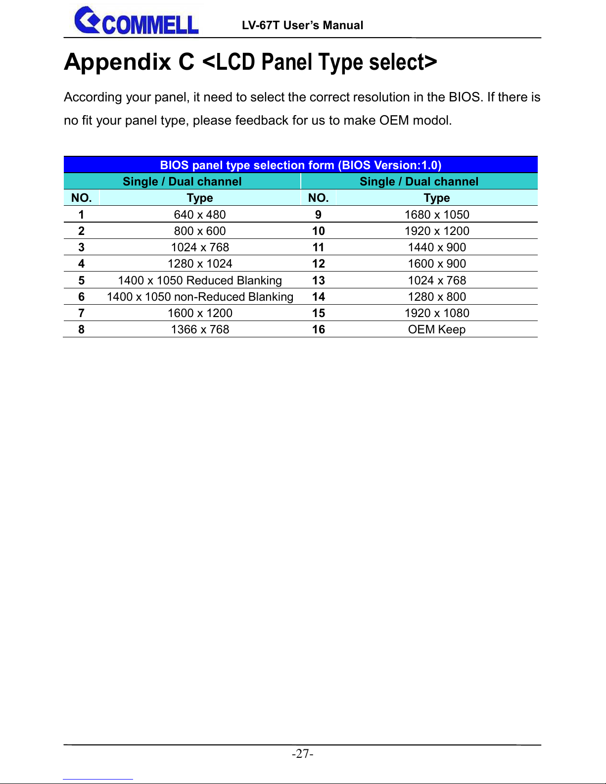
Appendix C <LCD Panel Type select>
According your panel, it need to select the correct resolution in the BIOS. If there is
no fit your panel type, please feedback for us to make OEM modol.
BIOS panel type selection form (BIOS Version:1.0)
Single / Dual channel
Single / Dual channel
NO.
Type
NO.
Type
1
640 x 480
9
1680 x 1050
2
800 x 600
10
1920 x 1200
3
1024 x 768
11
1440 x 900
4
1280 x 1024
12
1600 x 900
5
1400 x 1050 Reduced Blanking
13
1024 x 768
6
1400 x 1050 non-Reduced Blanking
14
1280 x 800
7
1600 x 1200
15
1920 x 1080
8
1366 x 768
16
OEM Keep
Page 29
LV-67T User’s Manual
-28-
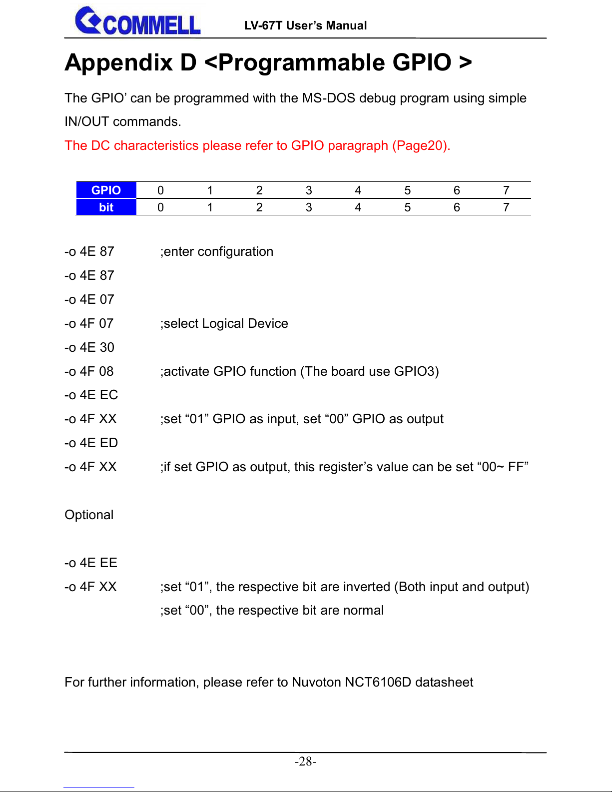
Appendix D <Programmable GPIO >
The GPIO’ can be programmed with the MS-DOS debug program using simple
IN/OUT commands.
The DC characteristics please refer to GPIO paragraph (Page20).
GPIO
0 1 2 3 4 5 6
7
bit 0 1 2 3 4 5
6
7
-o 4E 87 ;enter configuration
-o 4E 87
-o 4E 07
-o 4F 07 ;select Logical Device
-o 4E 30
-o 4F 08 ;activate GPIO function (The board use GPIO3)
-o 4E EC
-o 4F XX ;set “01” GPIO as input, set “00” GPIO as output
-o 4E ED
-o 4F XX ;if set GPIO as output, this register’s value can be set “00~ FF”
Optional
-o 4E EE
-o 4F XX ;set “01”, the respective bit are inverted (Both input and output)
;set “00”, the respective bit are normal
For further information, please refer to Nuvoton NCT6106D datasheet
Page 30
LV-67T User’s Manual
-29-
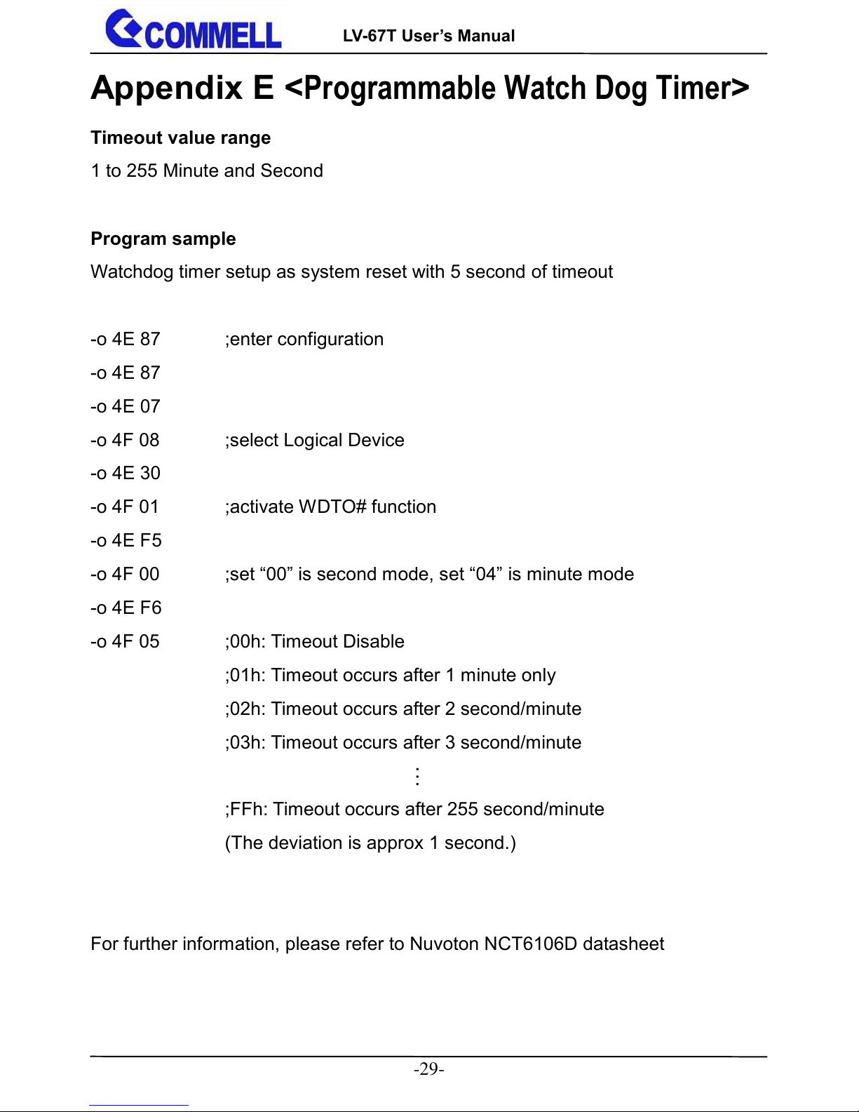
Appendix E <Programmable Watch Dog Timer>
Timeout value range
1 to 255 Minute and Second
Program sample
Watchdog timer setup as system reset with 5 second of timeout
-o 4E 87 ;enter configuration
-o 4E 87
-o 4E 07
-o 4F 08 ;select Logical Device
-o 4E 30
-o 4F 01 ;activate WDTO# function
-o 4E F5
-o 4F 00 ;set “00” is second mode, set “04” is minute mode
-o 4E F6
-o 4F 05 ;00h: Timeout Disable
;01h: Timeout occurs after 1 minute only
;02h: Timeout occurs after 2 second/minute
;03h: Timeout occurs after 3 second/minute
;FFh: Timeout occurs after 255 second/minute
(The deviation is approx 1 second.)
For further information, please refer to Nuvoton NCT6106D datasheet
…
Page 31

LV-67T User’s Manual
-30-
Appendix F <SATA RAID function setting>
When use RAID function, it need to enter the BIOS set RAID mode first.
[Advanced] > [Intel Advanced Menu] > [PCH-IO Configuration] >
[SATA Configuration] > [SATA Mode Selection] > [RAID]
At boot time, press <CTRL + I> to enter the RAID configuration menu.
It can be set the BIOS configuration below to extend the stay time of the option
boot ROM.
[SATA Configuration] > [Software Feature Mask Configuration] >
[OROM UI Normal Delay] (Need to set RAID mode first)
Page 32

LV-67T User’s Manual
-31-
Contact information
Any advice or comment about our products and service, or anything we can help
you please don’t hesitate to contact with us. We will do our best to support you for
your products, projects and business.
Taiwan Commate computer Inc.
Address
19F., NO.94, Sec. 1, Xintai 5th Rd., Xizhi Dist., New Taipei
City 22102, Taiwan.
TEL
+886-2-26963909
FAX
+886-2-26963911
Website
www.commell.com.tw
E-mail
info@commell.com.tw (General infomation)
tech@commell.com.tw (Technical Support)
Commell is a brand name of Taiwan Commate computer Inc.
 Loading...