

Page 1
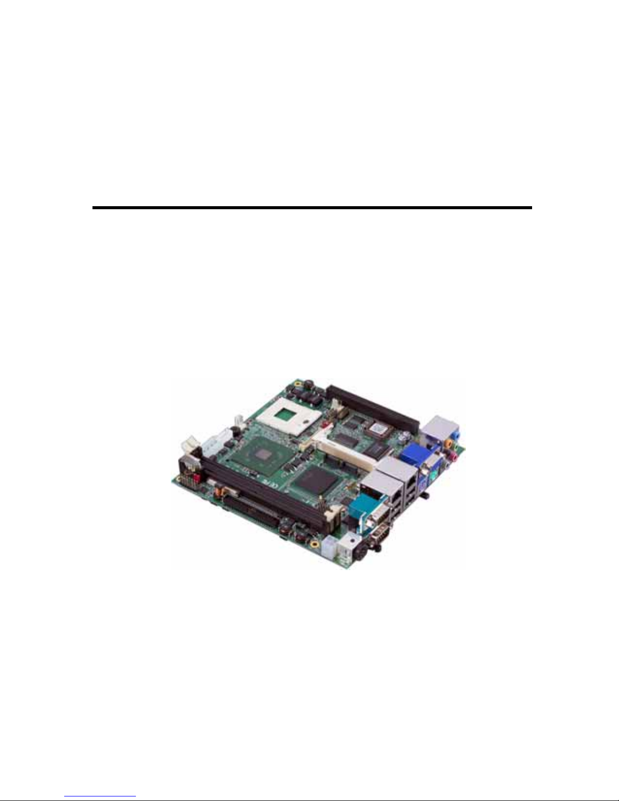
LV-673(E) Serial
Mini-ITXexpress Motherboard
User’s Manual
Edition 1.3
2009/01/12
Page 2

LV-673(E) User’s Manual
2
Copyright
Copyright 2008, all rights reserved. This document is copyrighted and all rights are
reserved. The information in this document is subject to change without prior notice to
make improvements to the products.
This document contains proprietary informat ion and protected by copyright. No part of
this document may be reproduced, copied, or translated in any form or any means
without prior written permission of the manufacturer.
All trademarks and/or registered trademarks contains in this document are property of
their respective owners.
Disclaimer
The company shall not be liable for any incidental or consequential dam ages resulting
from the performance or use of this product.
The company does not issue a warranty of any kind, express or implied, including
without limitation implied warranties of merchantability or fitness for a particular purpose.
The company has the right to revise the manual or include changes in the specifications
of the product described within it at any time without notice and without obligation to
notify any person of such revision or changes.
Trademark
All trademarks are the property of their respective holders.
Any questions please visit our website at TUhttp://www.commell.com.twUT
Page 3
LV-673(E) User’s Manual
3
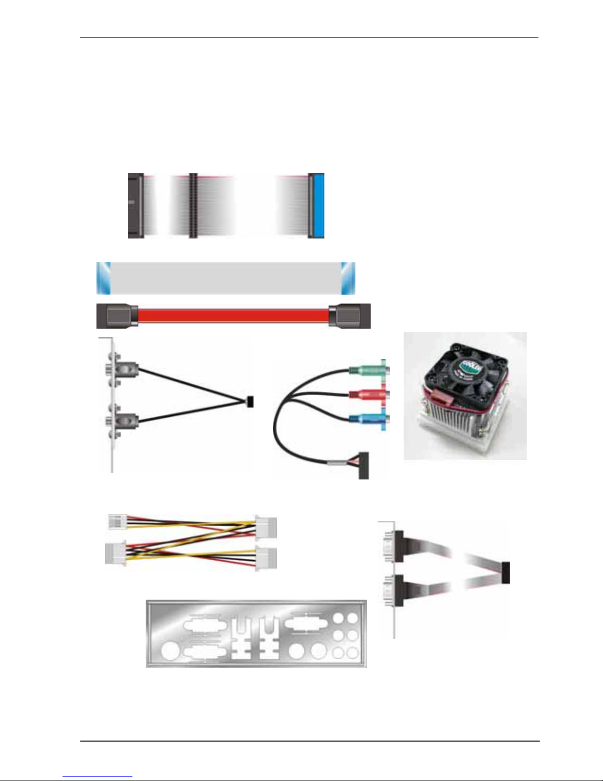
Packing List:
Please check the package content before you starting using the board.
Hardware:
LV-673(E) motherboard x 1
Cable Kit:
44-pin
44-pin
40-pin
Floppy Cable x 1
SATA Cable x 1
ATA33 IDE Cable x1
SDTV Cable x 1 (Only LV-673)
COM port Cable x 1
I/O Shield x 1
CPU Cooler x 1
4-pin to 4-pin Power Cable x 1
Printed Matters:
Driver CD (Including User’s Manual) x 1
YPbPr Cable x 1 (Only LV-673)
Page 4

LV-673(E) User’s Manual
4
Index
Chapter 1 <Introduction>...............................................................7
1.1 <Product Overview> .................................................................7
1.2 <Product Specification>............................................................8
1.3 <Mechanical Drawing>...........................................................10
1.4 <Block Diagram>.................................................................... 11
Chapter 2 <Hardware Setup>....................................................13
2.1 <Connector Location>.............................................................13
2.2 <Jumper Location & Reference>............................................14
2.3 <Connector Reference>...........................................................15
2.3.1 <Internal Connectors> .........................................................15
2.3.2 <External Connectors> ........................................................15
2.4 <CPU and Memory Setup>.....................................................16
2.4.1 <CPU Setup>.....................................................................16
2.4.2 <Memory Setup>................................................................17
2.5 <CMOS Setup>.......................................................................18
2.6 <Enhanced IDE Interface>......................................................19
2.7 <Serial ATA Interface>............................................................19
2.8 <Floppy Port>..........................................................................20
2.9 <Ethernet Interface>................................................................21
2.10 <Onboard Display Interface>................................................22
2.10.1 <Analog Display>.............................................................22
2.10.2 <Digital Display>..............................................................23
2.10.3 <HDTV Interface> LV-673(E) not supports TV out function......27
2.11 <Integrated Audio Interface> ................................................28
2.12 <GPIO Interface>..................................................................30
2.13 <Power Supply>....................................................................31
2.13.1 <Power Input>..................................................................31
2.13.2 <Power Output>................................................................32
2.14 <Switch and Indicator>.........................................................33
Page 5

LV-673(E) User’s Manual
5
Chapter 3 <System Setup>.........................................................34
3.1 <Video Memory Setup> ..........................................................34
Chapter 4 <BIOS Setup>..............................................................36
Appendix A <I/O Port Pin Assignment>............................38
A.1 <IDE Port>..............................................................................38
A.2 <Serial ATA Port>...................................................................39
A.3 <Floppy Port>.........................................................................39
A.4 <IrDA Port>............................................................................39
A.5 <Serial Port>...........................................................................40
A.6 <VGA Port>............................................................................41
A.7 <LAN Port>............................................................................41
A.8 < USB Interface >...................................................................41
Appendix B <Flash BIOS>...........................................................42
B.1 <Flash Tool>...........................................................................42
B.2 <Flash BIOS Procedure>........................................................42
Appendix C <System Resources>........................................43
C1. <I/O Port Address Map>.........................................................43
C2. <Memory Address Map>........................................................45
C3. <System IRQ & DMA Resources>.........................................46
C4. <GPIO programmed> .............................................................47
C5. <Watchdog Timer Setting>.....................................................48
Contact Information.........................................................................49
Page 6

LV-673(E) User’s Manual
6
(This Page is Left for Blank)
Page 7

LV-673(E) User’s Manual
Product Specification
7
Chapter 1 <Introduction>
1.1 <Product Overview>
LV-673(E) is the new generation of the Mini-ITX motherboard, with supporting last Intel
Pentium M processors for 533MHz front side bus, Intel 915GM(E) and ICH6-M chipset,
integrated GMA900 graphics, DDR2 memory, REALTEK High Definition Audio, Serial
ATA, PCI Express 16x interface and dual Gigabit LAN.
New Intel Pentium M Processor
The board supports last Intel Pentium M processors with 533MHz front si de bus, 2MB
L2 cache, to provide more powerful performance than before.
New features for Intel 915GM(E) chipset
The board integrates Intel 915GM(E) and ICH6-M chipset, to provide new generation o f
the mobile solution, supports Intel GMA900 graphics, DDR2 400/533 m emory, built-in
high speed mass storage interface of serial ATA, High Definition Audio with 7.1 channels
surrounding sound.
All in One multimedia solution
Based on Intel 915GM(E) and ICH6-M chipset, the board provides high performance
onboard graphics, 18-bit dual channel LVDS interface, HDTV and 7.1 channels High
Definition Audio, to meet the very requirement of the multimedia application.
LV-673(E) not supports TV out function.
Flexible Extension Interface
The board provides one PCI-Express 16x slots for graphics card, it also can support
PCI-Express 1x for LAN card or other devices. The board also provides one PCMCIA
Type II slot, CompactFlash Type I slot and one mini-PCI slot.
Page 8

LV-673(E) User’s Manual
8
1.2 <Product Specification>
General Specification
Form Factor Mini-ITX motherboard
CPU Intel® Pentium M / Celeron M processors
Package type: FC-PGA478
L2 Cache: 512KB/1MB/2MB
Front side bus: 400/533MHz
( The Intel® Celeron® M Processor 4xx series can not be used
on LV-673(E) series .)
Memory 2 x 240-pin DDR2 400/533MHz SDRAM up to 2GB
Up to 8GB/s of bandwidth with dual-channel interleaved mode
Dual-Channel technology supported
Unbufferred, none-ECC memory supported only
Chipset Intel® 915GM(E) (Northbridge) and ICH6-M (Southbridge)
BIOS Phoenix-Award v6.00PG 4Mb PnP flash BIOS
Green Function Power saving mode includes doze, standby and suspend modes.
ACPI version 1.0 and APM version 1.2 compliant
Watchdog Timer System reset programmable watchdog timer with 1 ~ 255 sec./min. of
timeout value
Real Time Clock Intel® ICH6-M built-in RTC with lithium battery
Enhanced IDE UltraDMA33 IDE interface supports up to 2 ATAPI devices
One 44-pin IDE port onboard
One CompactFlash Type I socket on solder side
Serial ATA Intel® ICH6-M integrates 2 Serial ATA interfaces
Up to 150MB/s of transfer rate
Multi-I/O Port
Chipset Intel® ICH6-M with Winbond® W83627THF controller
Serial Port Two external and two internal RS-232 serial ports
USB Port Six Hi-Speed USB 2.0 ports with 480Mbps of transfer rate
Parallel Port None
Floppy Port One slim type Floppy port
IrDA Port One IrDA compliant Infrared interface supports SIR
K/B & Mouse External PS/2 keyboard and mouse ports on rear I/O panel
GPIO One 12-pin Digital I/O connector with 8-bit programmable I/O interface
Smart Fan One CPU fan connectors for fan speed controllable
VGA Display Interface
Chipset Intel® 915GM(E) GMCH (Graphic Memory Controller Hub)
Frame Buffer Up to 128MB shared with system memory
Display Type CRT, LCD monitor with analog display
Onboard 18-bit dual channel LVDS interface
Onboard HDTV interface
Connector External DB15 female connector on rear I/O panel
Page 9

LV-673(E) User’s Manual
Product Specification
9
Onboard 40-in LVDS connector
Onboard 8-pin TV-out connector
Ethernet Interface
Controller Marvell E8053 PCI Express Gigabit Ethernet controller
Type Triple speed 10/100/1000Base-T
auto-switching Fast Ethernet
Full duplex, IEEE802.3U compliant
Connector Dual External RJ45 connectors with LED on rear I/O panel
Audio Interface
Chipset Intel® ICH6M with Realtek® ALC880 codec
Intel High Definition Audio compliance
Interface 7.1 channels sound output
Connector External Audio phone jack for Line-out, Line-in, MIC-in, Surround,
Center and Backsurround
Onboard audio connector with pin header (built-in amplifier for speaker
out)
Onboard CD-IN connector
Expansive Interface
PCI-Express One 16x PCI-Express slot (compatible with 1x slot)
Up to 8GB/s of transfer bandwidth
Power supply: +3.3V, +12V
PCI One Mini-PCI socket for TYPE III (32-bit, 33MHz)
Power supply: +3.3V, +5V
PCMCIA One PCMCIA Type II slot on solder side with RICOH R5C475II
controller
Power and Environment
Power
Requirement
DC 12V input with external DC mini DIN or onboard 4-pin connector
Input Range 10.5V ~ 13V
Dimension 170 (L) x 170 (H) mm
Temperature Operating within 0 ~ 60P
o
P
C (32 ~ 140P
o
P
F)
Storage within -20 ~ 85P
o
P
C (-4 ~ 185P
o
P
F)
Ordering Code
LV-673(E) Intel Pentium M platform with onboard VGA, HD audio, SATA
USB2.0, LVDS, HDTV, PCI-Express, Mini-PCI, CF, PCMCIA
4 x COM
LV-673(E) not supports TV out function.
PCIE-SDVOD PCI-Express add-on card for single DVI interface
The specifications may be different as the actual production.
For further product information please visit the website at TUhttp://www.commell.com.tw
UT
Page 10
LV-673(E) User’s Manual
Mechanical Drawing
10
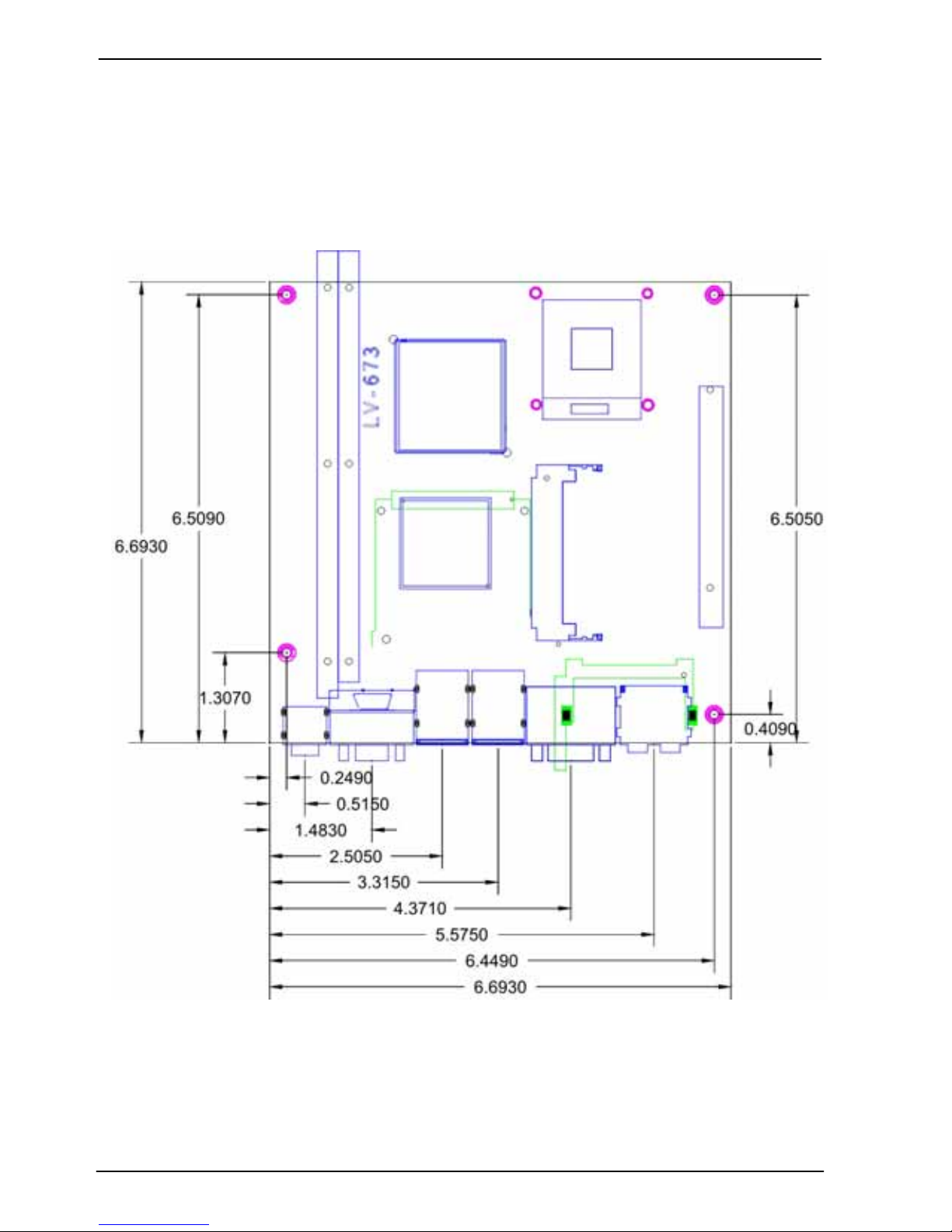
1.3 <Mechanical Drawing>
Page 11
LV-673(E) User’s Manual
Block Diagram
11
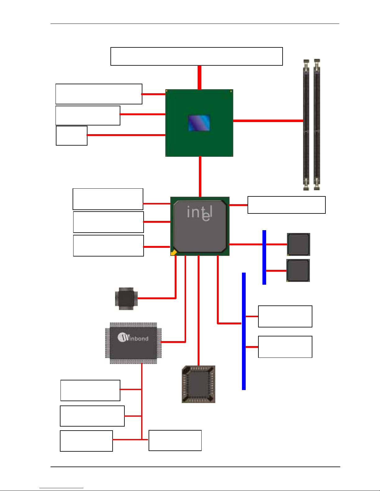
1.4 <Block Diagram>
Intel Pentium M/Celeron M Processors
Intel GMA900 Graphics
PCI-Express x16
LVDS
2 x 240-pin DDR2
400/533MHz up to
2GB
915GM(E)
ICH6-M
2 x Serial ATA ports
PCI Express 1x
6 x USB2.0 ports
Marvell E8053
Gigabit LAN
PCI
Mini-PCI slot
UltraDMA33 IDE
CompactFlash
PCMCIA
BIOS
HD Audio
4 x Serial ports
1 x Floppy ports
8-bit GPIO
IrDA
Page 12

LV-673(E) User’s Manual
12
(This Page is Left for Blank)
Page 13
LV-673(E) User’s Manual Hardware Setup
Connector Location
13
Chapter 2 <Hardware Setup>
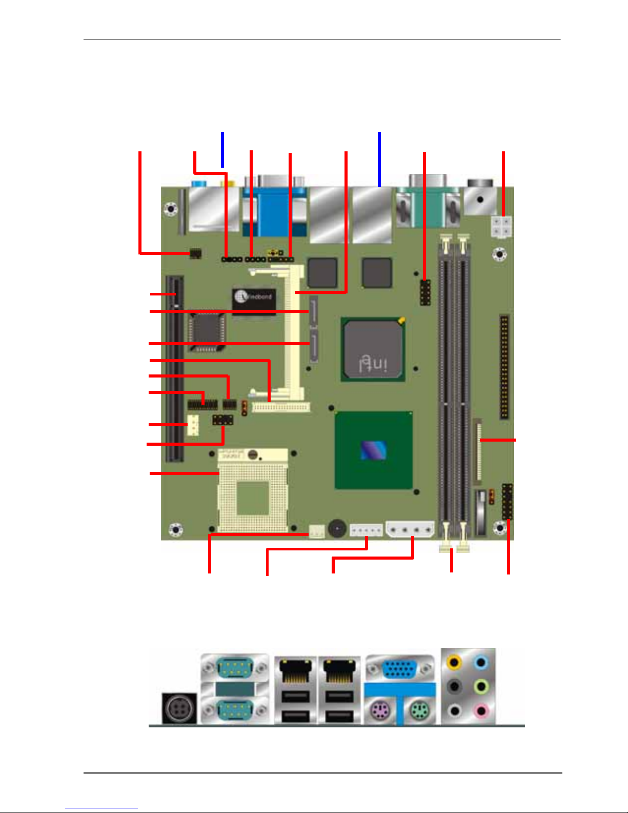
2.1 <Connector Location>
CN_AUDIO SPDIF CDIN CN_IR MINIPCI CN_USB PWRIN
PEG
SATA1
SATA2
CN_LVDS
CN_DIO
CN_COM34
CPUFAN
CN_TV
CPU
SYSFAN CN_INV CN_BPWR DDRIIB/A JFRNT
IDE
FDD
Solder side: CF CARDBUS
DC_IN COM1/2 USB_RJ45_A/B KB MS AUDIO
VGA
Page 14
LV-673(E) User’s Manual Hardware Setup
Jumper Location & Reference
14
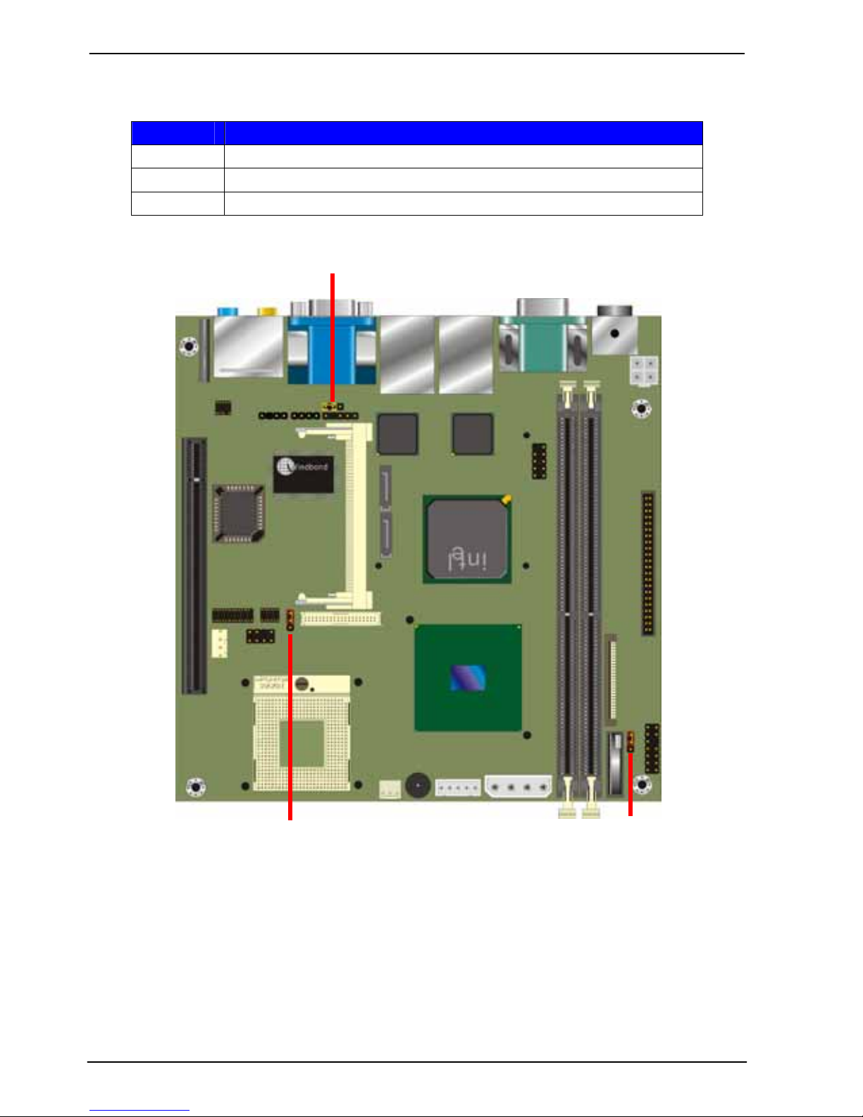
2.2 <Jumper Location & Reference>
Jumper Function
JRTC CMOS Operating/Clear Setting
JCFSEL CF with IDE mode selection
JVLCD Panel Voltage Setting
JCFSEL
JVLCD
JRTC
Page 15
LV-673(E) User’s Manual Hardware Setup
Connector Location
15
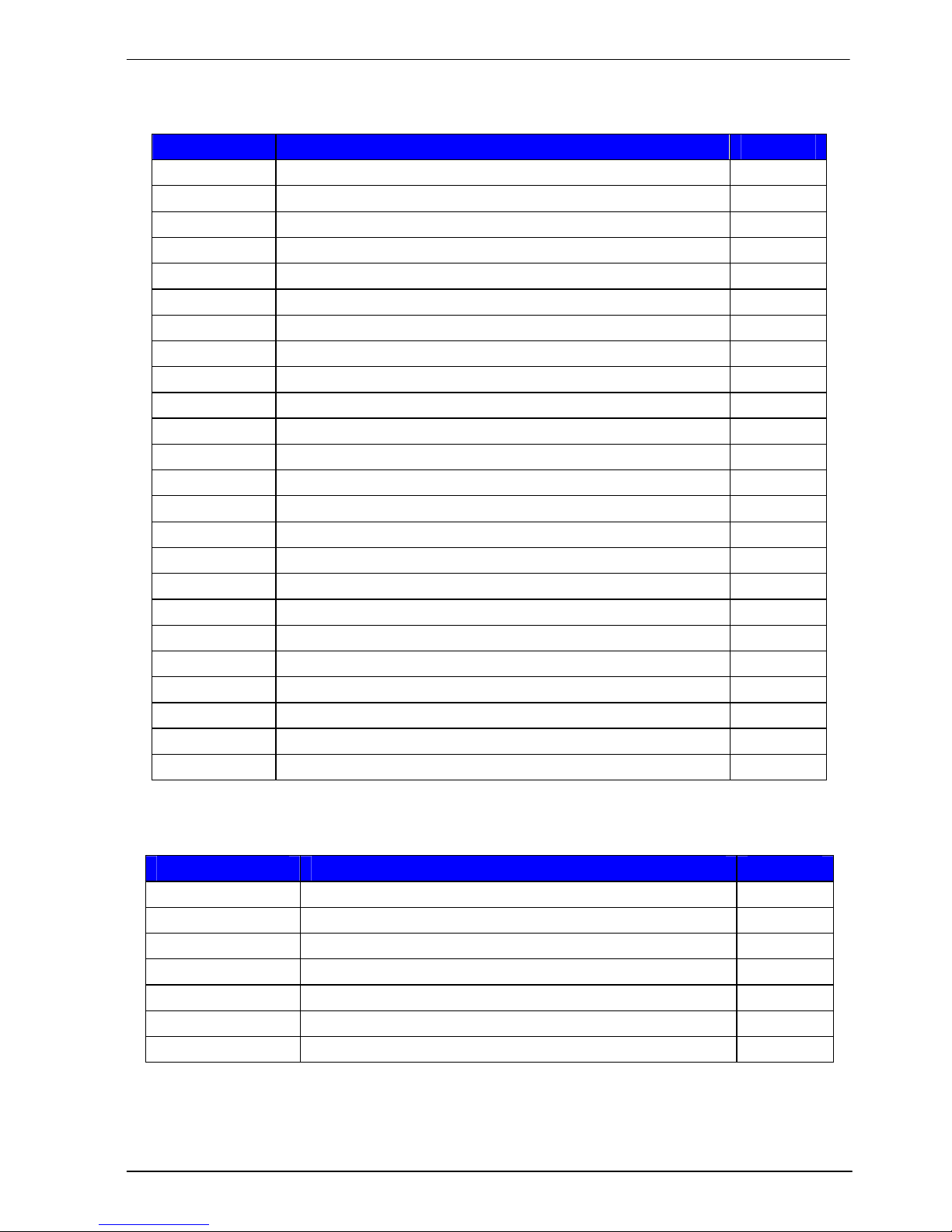
2.3 <Connector Reference>
2.3.1 <Internal Connectors>
Connector Function Remark
CPU Socket479 for CPU Standard
DDRIIA/B 240 -pin DDR2 SDRAM DIMM socket Standard
IDE 44-pin IDE connector Standard
FDD 26-pin slim type floppy connector Standard
S_ATA1/2 7-pin Serial ATA connector Standard
PWRIN 4-pin power input connector Standard
CN_BPWR 4-pin power output connector Standard
CN_AUDIO 5 x 2-pin audio connector Standard
SPDIF 4-pin S/PDIF digital audio output connector Standard
CDIN 4-pin CD-ROM audio input connector Standard
CN_DIO 6 x 2-pin digital I/O connector Standard
CN_USB 5 x 2-pin USB connector Standard
CPUFAN 4-pin CPU cooler fan connector Standard
SYSFAN 3-pin system cooler fan connector Standard
CN_LVDS 20 x 2-pin LVDS connector Standard
CN_INV 5-pin LCD inverter connector Standard
CN_IR 5-pin IrDA connector Standard
CN_COM34 10 x 2-pin COM3 & COM4 connector Standard
CN_TV 4 x 2-pin TV-out connector (Only LV-673) Standard
JFRNT 14-pin front panel switch/indicator connector Standard
MINIPCI Mini-PCI socket Standard
PEG PCI Express 16x/1x slot Standard
CF CompactFlash Type I socket Standard
CARDBUS PCMCIA Type II slot Standard
2.3.2 <External Connectors>
Connector Function Remark
DC_IN DC 12V input connector Standard
COM1/2 Serial port connector Standard
USB_RJ45_A/B Dual USB and RJ45 LAN connector Standard
VGA DB15 analog VGA connector Standard
KB PS/2 keyboard connector Standard
MS PS/2 mouse connector Standard
AUDIO Audio connectors Standard
Page 16
LV-673(E) User’s Manual Hardware Setup
CPU & Memory Setup
16
2.4 <CPU and Memory Setup>
2.4.1 <CPU Setup>
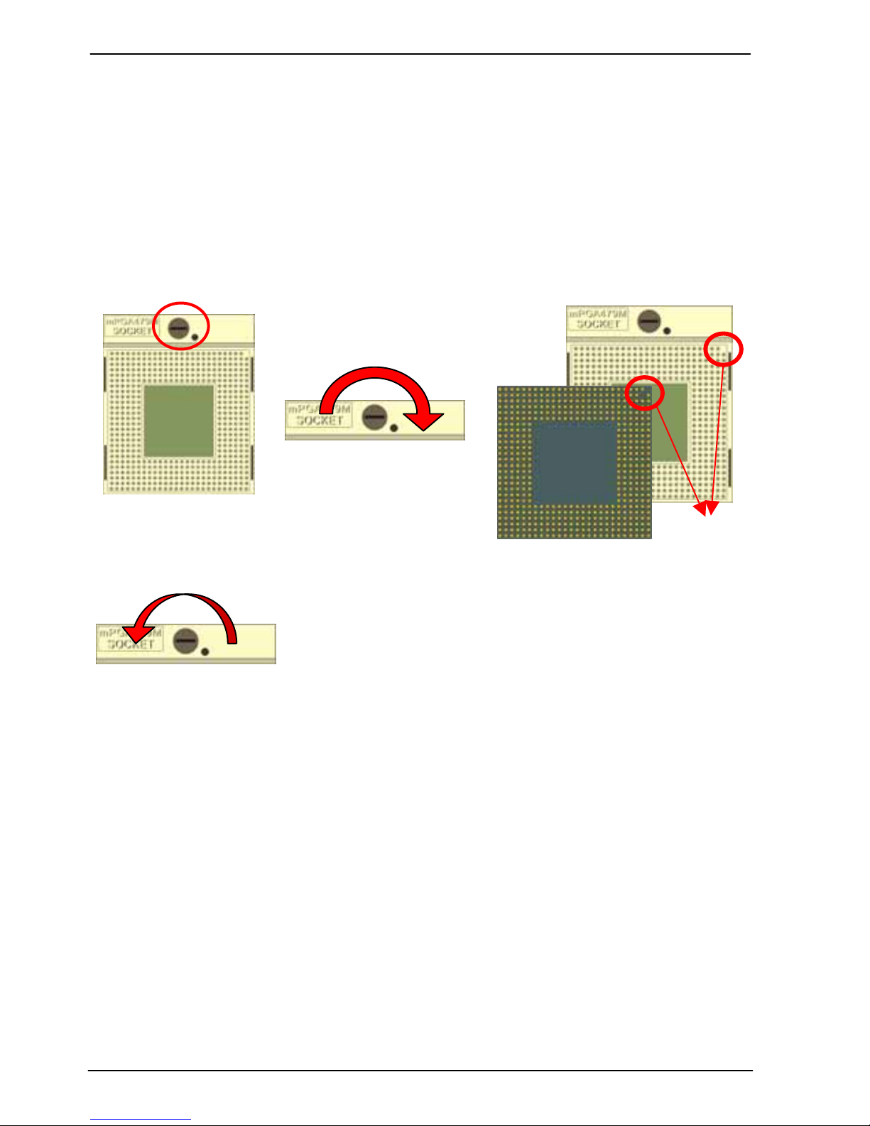
The board comes with the socket479 for Intel Pentium M/Celeron M processors, it
supports new generation of Intel Pentium M processors with 533MHz of front side bus
and 2MB L2 cache. Please follow the instruction to install the CPU properly.
1. Use the flat-type
screw drive to unlock
the CPU socket
Unlock wa
y
Check point
2. Follow the pin direction to install
the processor on the socket
3. Lock the socket
Page 17
LV-673(E) User’s Manual Hardware Setup
Memory Setup
17
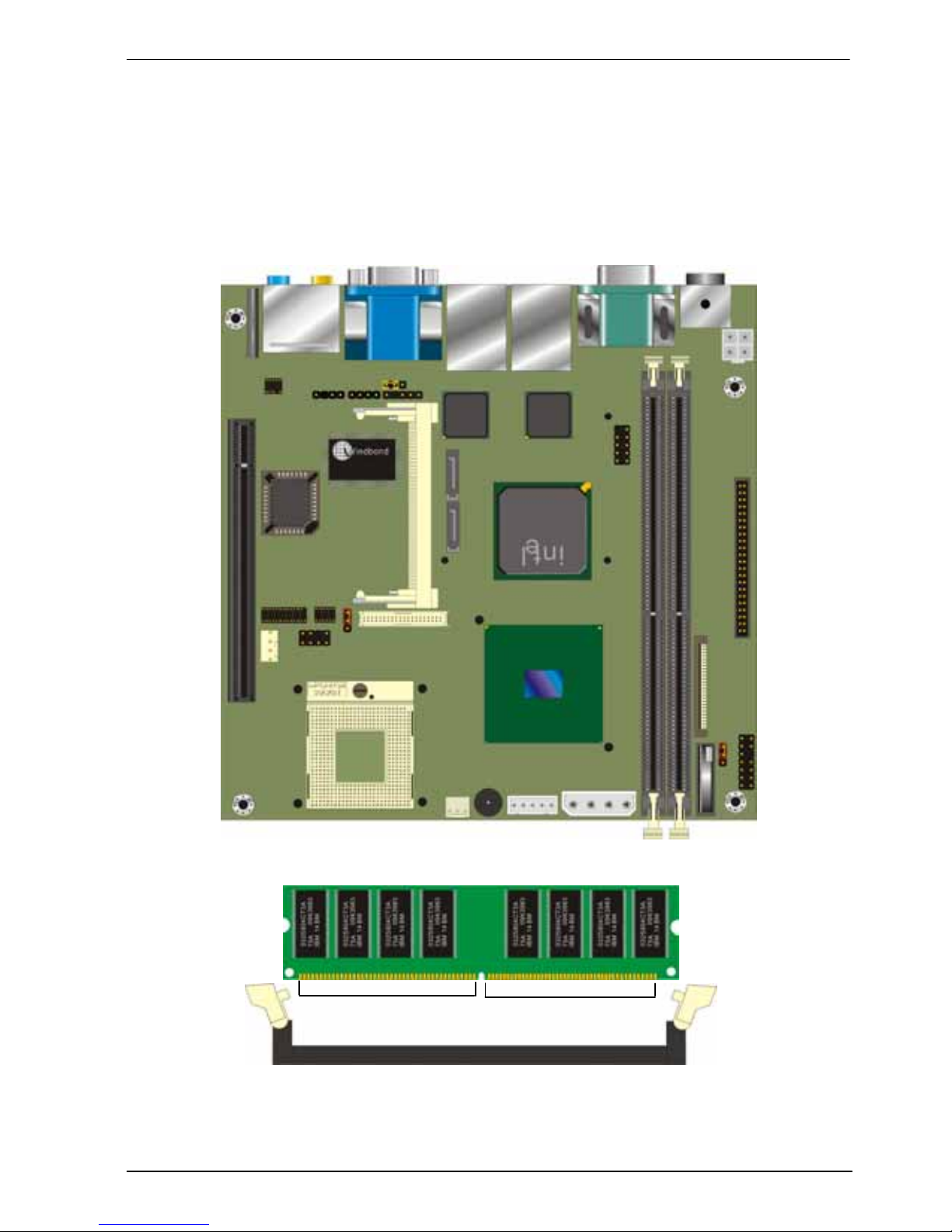
2.4.2 <Memory Setup>
The board provides two 240-pin DDR2 DIMMs to support DDR2 400/533 memory
modules up to 2GB of capacity. Non-ECC, unbuffered memory is supported only. While
applying two same modules, dual channel technology is enabled automatically for
higher performance.
DDRIIB/A
112-pin128-pin
Please check the pin number to match the socket side well
before installing memory module.
Page 18
LV-673(E) User’s Manual Hardware Setup
CMOS Setup
18
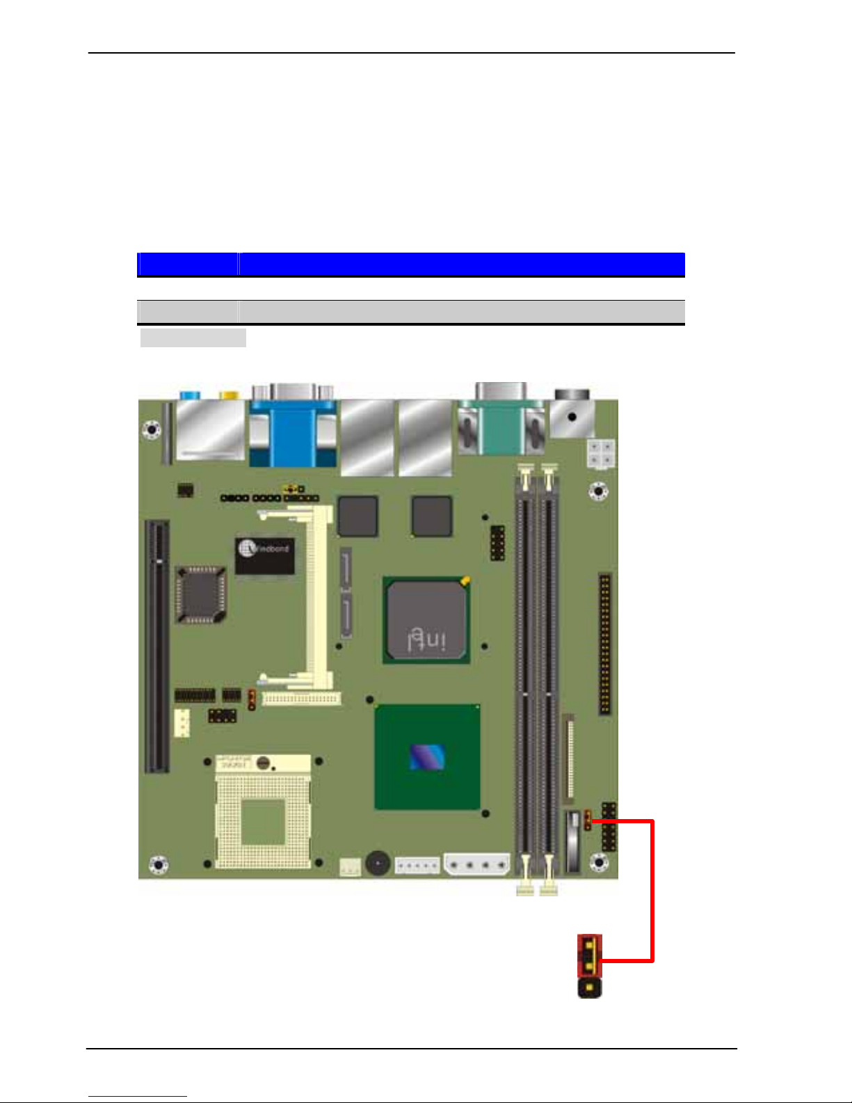
2.5 <CMOS Setup>
The board’s data of CMOS can be setting in BIOS. If the board refus es to boot due to
inappropriate CMOS settings, here is how to proceed to clear (reset) the CMOS to its
default values.
Jumper: JRTC
Type: Onboard 3-pin jumper
JRTC Mode
1-2 Clear CMOS
2-3 Normal Operation
Default setting
JRTC
1
3
Page 19
LV-673(E) User’s Manual Hardware Setup
Enhanced IDE Interface
19
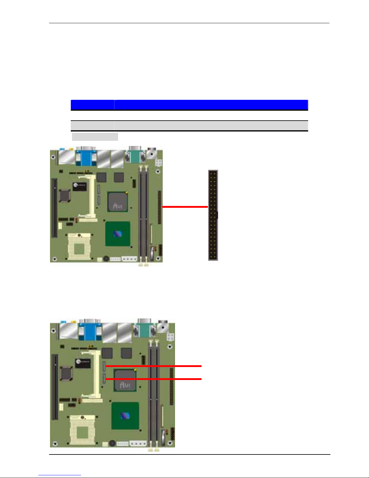
2.6 <Enhanced IDE Interface>
The board has one UltraDMA33 IDE interface to support up to 2 ATAPI devices, and one
CompactFlash Type I socket on the solder side, with jumper JCFSEL for IDE
master/slave mode selection.
Jumper: JCFSEL
Type: onboard 3-pin header
JCFSEL Mode
1-2 Master
2-3 Slave
Default setting
2.7 <Serial ATA Interface>
Based on Intel ICH6-M, the board provides two Serial ATA interfaces with up to 150MB/s
of transfer rate.
SATA1
SATA2
IDE
44
1
2
43
Page 20
LV-673(E) User’s Manual Hardware Setup
Floppy Port
20
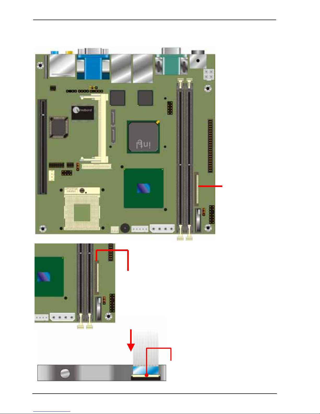
2.8 <Floppy Port>
The board provides one slim type floppy port.
FDD
4. Lift up this plastic bar
5. Slot the cable in (Blue paste for outside)
6. Press back the plastic bar
Floppy rear side
1. Lift up the brown plastic bar
2. Slot the cable in (Blue paste for
brown bar side)
3. Press back the plastic bar
Page 21
LV-673(E) User’s Manual Hardware Setup
Ethernet Interface
21
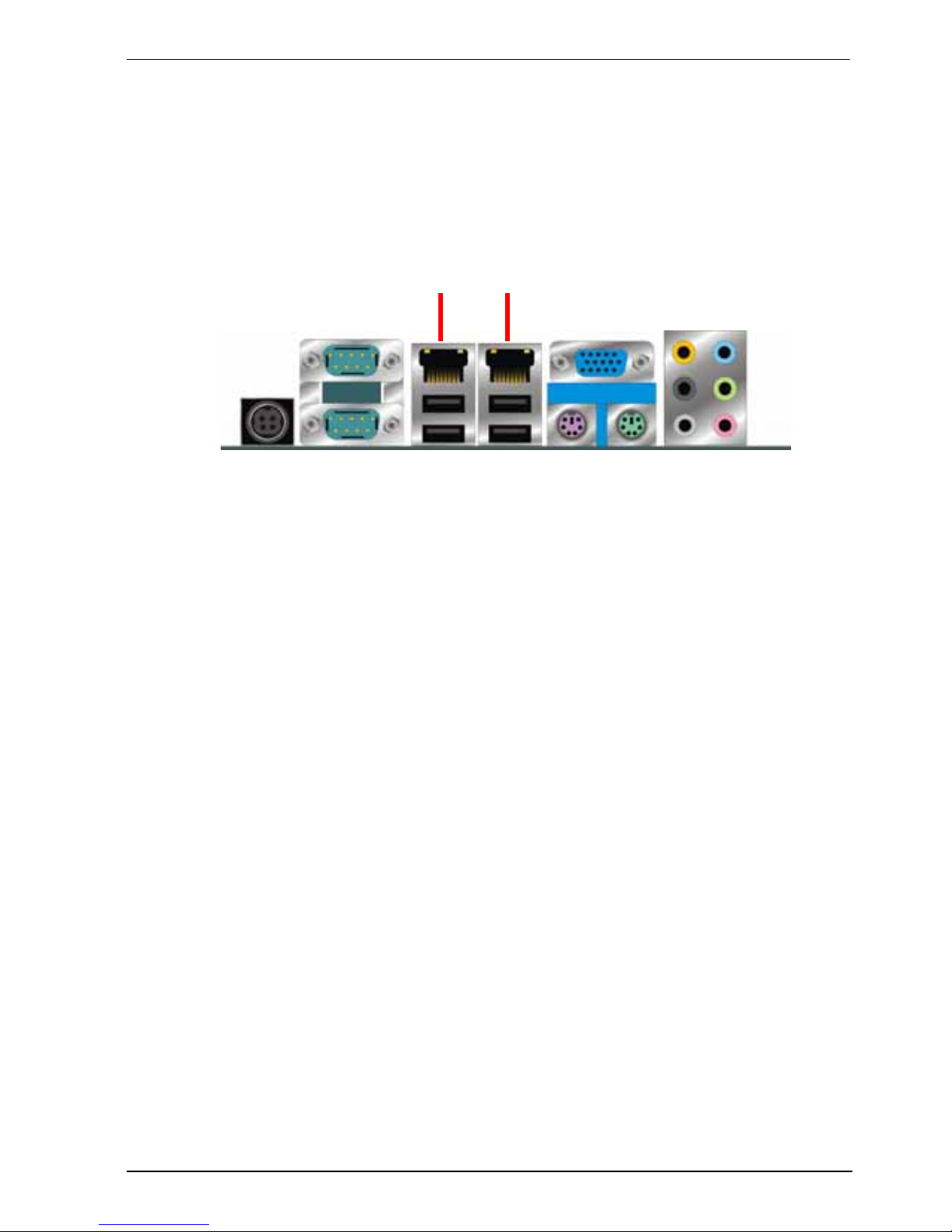
2.9 <Ethernet Interface>
The board integrates with two Marvell E8053 PCI Express Gigabit Ethernet controllers,
as the PCI Express 1x can speed up to 250MB/s of transfer rate instead of late PCI bus
with 133MB/s of transfer rate. The Marvell E8053 supports triple speed of
10/100/100Base-T, with IEEE802.3 compliance and Wake-On-LAN supported.
RJ45 LAN connector
Page 22
LV-673(E) User’s Manual Hardware Setup
Onboard Display Interface
22
2.10 <Onboard Display Interface>
Based on Intel 915GM(E) chipset with built-in GMA (Graphic Media Accelerator) 900
graphics, the board provides one DB15 connector on real external I/O port, and one
40-pin LVDS interface with 5-pin LCD backlight inverter connector. The board provides
dual display function with clone mode and ext ended desktop mode for CRT and LCD.
The board also provides DVO port on PCI Express slot to support DVI interface with add
on card.
Notice: When you install any PCI Express Graphic card, the onboard graphics would be
disabled automatically.
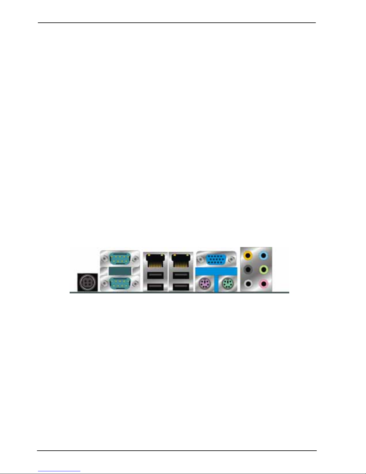
2.10.1 <Analog Display>
Please connect your CRT or LCD monitor with DB15 male connector to the onboard
DB15 female connector on rear I/O port.
VGA
Page 23
LV-673(E) User’s Manual Hardware Setup
Onboard Display Interface
23
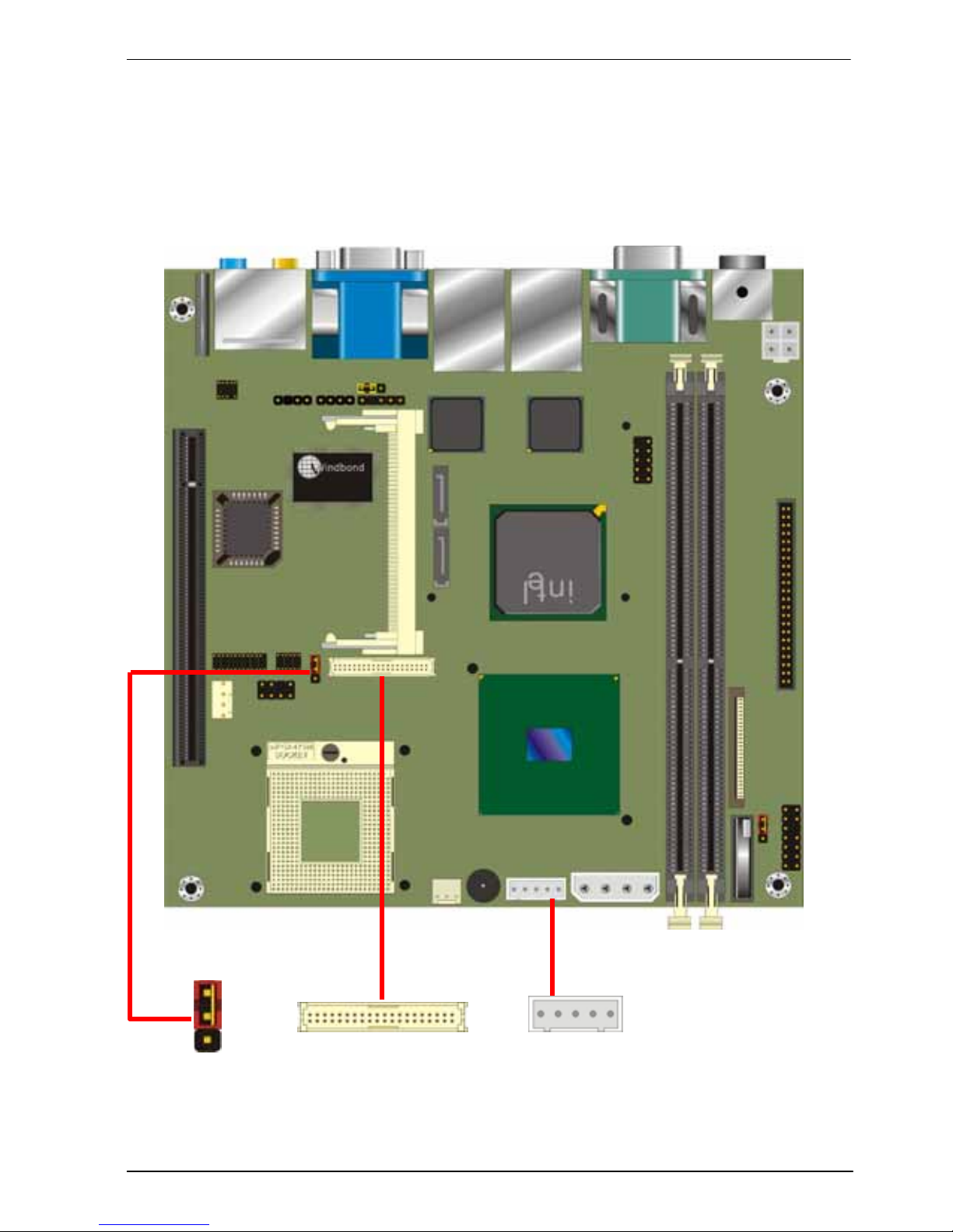
2.10.2 <Digital Display>
The board provides one 40-pin LVDS connector for 18-bit single/dual channel panels,
supports up to 1600 x 1200 (UXGA) and 1920 x 1200 (WUXGA) of resolution, with one
LCD backlight inverter connector and one jumper for panel voltage setting.
CN_LVDS
1
2
39
40
1 5
CN_INV
1
3
JVLCD
Page 24
LV-673(E) User’s Manual Hardware Setup
Onboard Display Interface
24
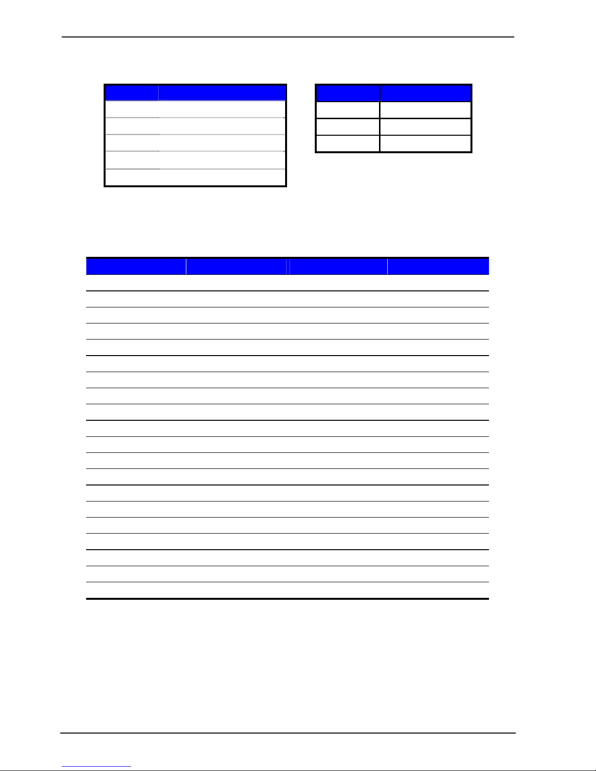
Connector: CN_INV Connector: JVLCD
Type: 5-pin LVDS Power Header Type: 3-pin Power select Header
Pin Description Pin Description
1 +12V 1 VCC
2 GND 2 LCDVCC
3 GND 3 VCC3
4 GND
5 ENABKL
Connector: CN_LVDS
Type: onboard 40-pin connector for LVDS connector
Connector model: HIROSE DF13-40DP-1.25V
Pin Signal Pin Signal
2 LCDVCC 1 LCDVCC
4 GND 3 GND
6 ATX0- 5 BTX0-
8 ATX0+ 7 BTX0+
10 GND 9 GND
12 ATX1- 11 BTX114 ATX1+ 13 BTX1+
16 GND 15 GND
18 ATX2- 17 BTX220 ATX2+ 19 BTX2+
22 GND 21 GND
24 ACLK- 23 N/C
26 ACLK+ 25 N/C
28 GND 27 GND
30 N/C 29 BCLK32 N/C 31 BCLK+
34 GND 33 GND
36 LVDDCLK 35 N/C
38 LVDDDAT 37 N/C
40 N/C 39 N/C
Page 25
LV-673(E) User’s Manual Hardware Setup
Onboard Display Interface
25
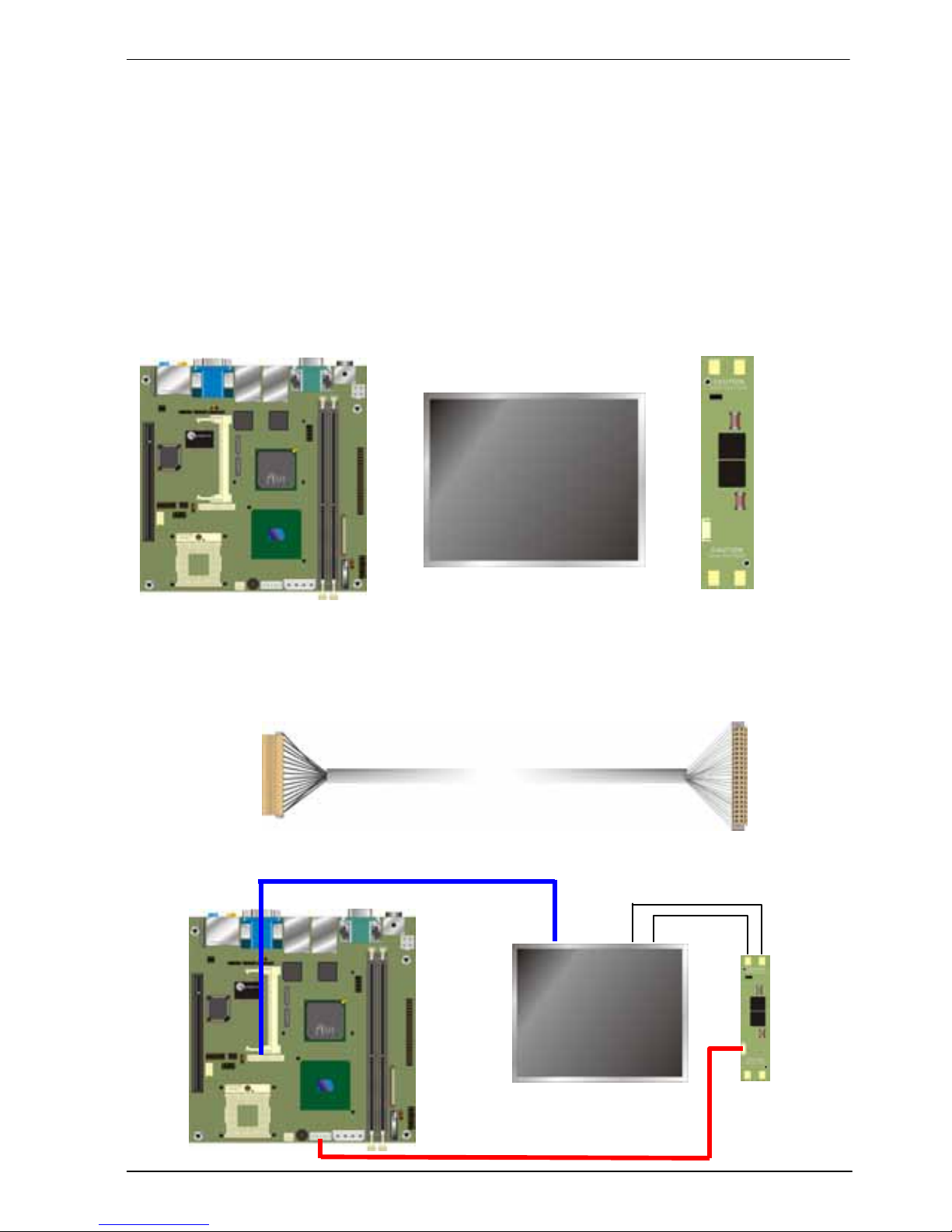
To setup the LCD, you need the component below:
1. A panel with LVDS interfaces.
2. An inverter for panel’s backlight power.
3. A LCD cable and an inverter cable.
For the cables, please follow the pin assignment of the conne ctor to make a c able, becaus e
every panel has its own pin assignment, so we do not pro vide a standard cable; ple ase find
a local cable manufacture to make cables.
LCD Installation Guide:
1. Preparing the LV-673(E), LCD panel and the backlight inverter.
2. Please check the datasheet of the panel to see the voltage of the panel, and set the
jumper JVLCD to +5V or +3.3V.
3. You would need a LVDS type cable.
4. To connect all of the devices well.
For sample illustrator only
Panel side
Board side
Page 26
LV-673(E) User’s Manual Hardware Setup
Onboard Display Interface
26
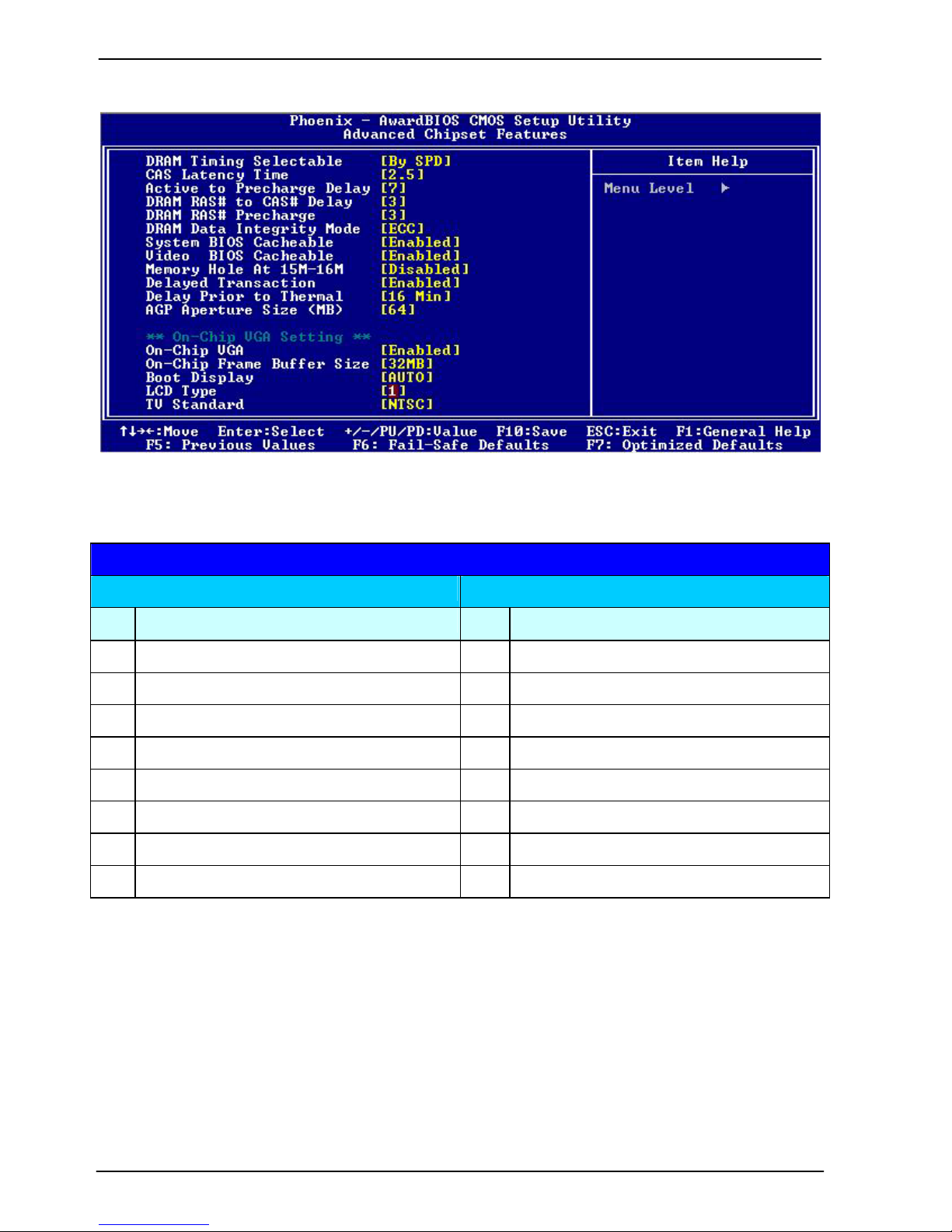
After setup the devices well, you need to select the LCD panel type in the BIOS.
The panel type mapping is list below:
BIOS panel type selection form
Single channel Dual channel
NO. Output format NO. Output format
1 640 x 480 9 1024 x 768
2 800 x 600 10 1280 x 768
3 1024 x 768 11 1280 x 1024
4 1280 x 768 12 1366 x 768
5 1280 x 1024 13 1400 x 1050 @ 108Mhz
6 14 1400 x 1050 @ 122Mhz
7 15 1600 x 1200
8 16 1920 x 1200
Page 27
LV-673(E) User’s Manual Hardware Setup
Onboard Display Interface
27
2.10.3 <HDTV Interface> LV-673(E) not supports TV out function.
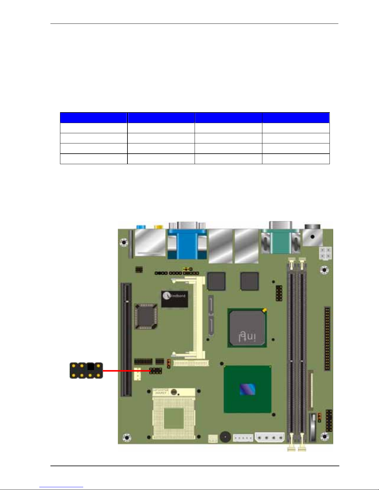
The board provides one HDTV interface up to 1024 x 768 resolution by NTSC/PAL
supported, for three output types with Composite, S-Video and Component (YPbPr).
Connector: CN_TV
Connector type: 8-pin header TV-out connector (pitch = 2.54mm)
Pin Number Assignment Pin Number Assignment
1 GND 2 S-Video/Y
3 S-video/Pr 4 GND
5 GND 6 GND
7 Composite/Pb 8 GND
Notice1: This connector is for both S-Video/Composite and YPbPr outputs; please use
attached two cables in the package for SDTV or HDTV devices.
Notice2: S-Video and Composite can not be used at the same time.
CN_TV
1
8
Page 28
LV-673(E) User’s Manual Hardware Setup
Integrated Audio Interface
28
2.11 <Integrated Audio Interface>
The board integrates onboard audio interface with REALT EK ALC880 codec, with Intel
next generation of audio standard as Hig h Definition Audio, it offers more vivid sound
and other advantages than former AC97 audio compliance.
The main specifications of ALC880 are:
High-performance DACs with 100dB S/N ratio
8 DAC channels support 16/20/24-bit PCM format for 7.1 audio solution
16/20/24-bit S/PDIF-OUT supports 44.1K/48K/96kHz sample rate
Compatible with AC'97
Meets Microsoft WHQL/WLP 2.0 audio requirements
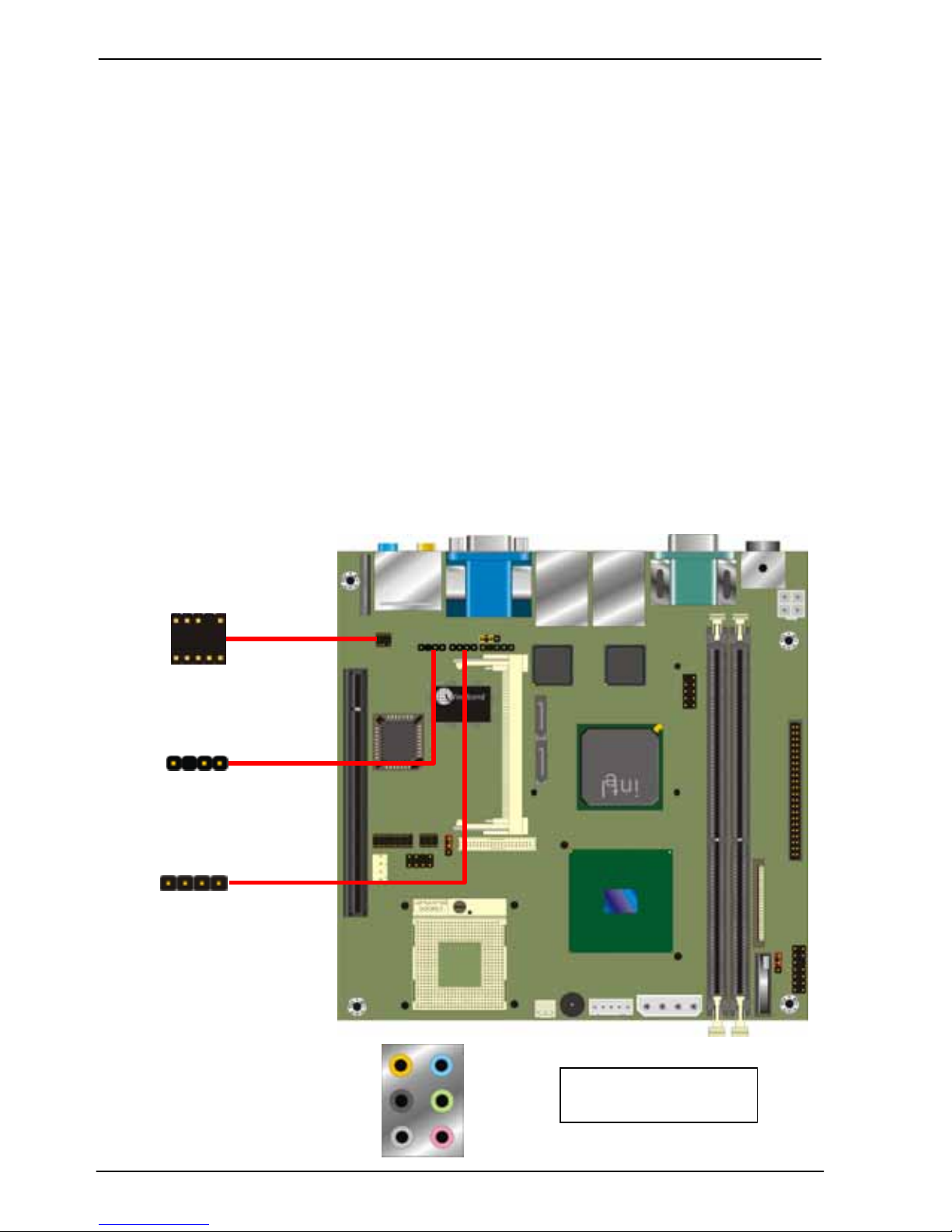
The board provides 7.1 channels audio phone jacks on rear I/O port, and amplified
speaker out and Line-in/MIC-in ports for front I/O panel through optional cable.
CN_AUDIO
1
10
SPDIF
1
CDIN
1
4
Rear I/O phone jacks
LINE-IN
LINE-OUT
MIC-IN
Cente
r
Rear Speake
r
Side Speake
r
Page 29

LV-673(E) User’s Manual Hardware Setup
Integrated Audio Interface
29
Connector: CN_AUDIO
Type: 10-pin (2 x 5) 1.27mm x 2.54mm-pitch header
Pin Description Pin Description
1 MIC_L 2 Ground
3 MIC_R 4 Ground
5 Speaker_R 6 MIC Detect
7 SENSE 8 N/C
9 Speaker_L 10 Speaker Detect
Connector: CDIN
Type: 4-pin header (pitch = 2.54mm)
Pin Description
1 CD – Left
2 Ground
3 Ground
4 CD – Right
Connector: SPDIF
Type: 4-pin header (pitch = 2.54mm)
Pin Description
1 +5V
2 N/C
3 SPDIFOUT
4 GND
Page 30
LV-673(E) User’s Manual Hardware Setup
GPIO Interface
30
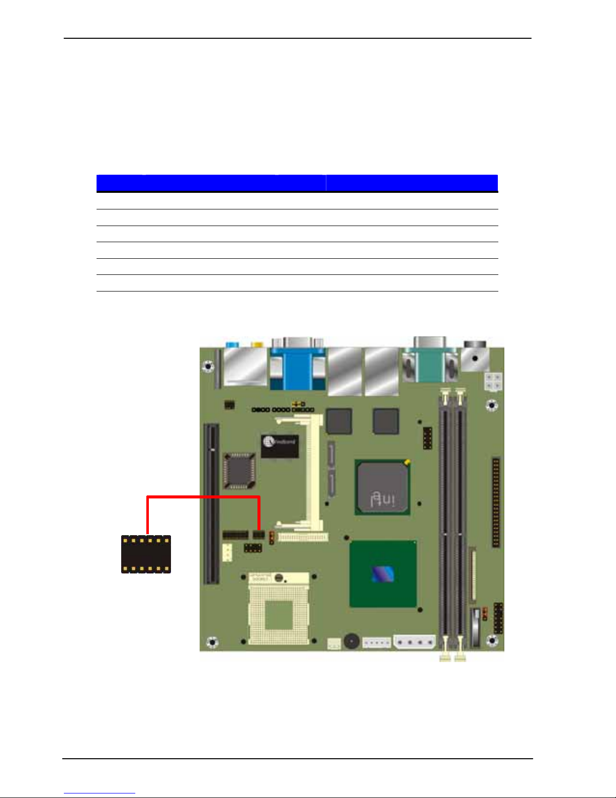
2.12 <GPIO Interface>
The board provides a programmable 8-bit digital I/O interface; you can use this general
purpose I/O port for system control like POS or KIOSK.
Connector: CN_DIO
Type: 12-pin (6 x 2) 1.27mm x 2.54mm-pitch header
Pin Description Pin Description
1 Ground 2 Ground
3 GP10 4 GP14
5 GP11 6 GP15
7 GP12 8 GP16
9 GP13 10 GP17
11 VCC 12 +12V
CN_DIO
1
12
Page 31
LV-673(E) User’s Manual Hardware Setup
Power Supply
31
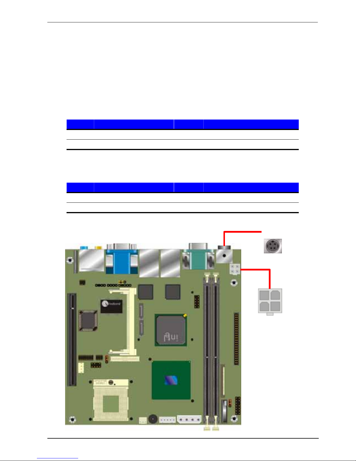
2.13 <Power Supply>
2.13.1 <Power Input>
The board requires DC 12V input with 4-pin mini DIN connector on rear I/O panel, or
onboard 4-pin ATX2.0 12V connector, the i nput voltage range is from 10.5V to 13V, for
the input current, please take a reference of the power consumption report on appendix.
Connector: PWRIN
Type: 4-pin standard ATX2.0 +12V power connector
Pin Description Pin Description
1 Ground 2 Ground
3 +12V 4 +12V
Connector: DC_IN
Type: 4-pin DC power connector
Pin Description Pin Description
1 +12V 2 +12V
3 Ground 4 Ground
PWRIN
12
34
DC_IN
12
4
3
Page 32
LV-673(E) User’s Manual Hardware Setup
Power Supply
32
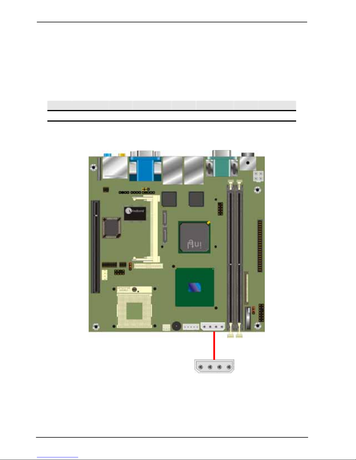
2.13.2 <Power Output>
The board provides one 4-pin AT connector for +5V/+12V output for powering your HDD,
CDROM or other devices.
Connector: CN_BPWR
Type: 4-pin P-type connector for +5V/+12V output
Pin Description Pin Description Pin Description Pin Description
1 +5V 2 Ground 3 Ground 4 +12V
Note: Maximum output voltage: 12V/5A & 5V/3A
CN_BPWR
14
Page 33
LV-673(E) User’s Manual Hardware Setup
Switch and Indicator
33
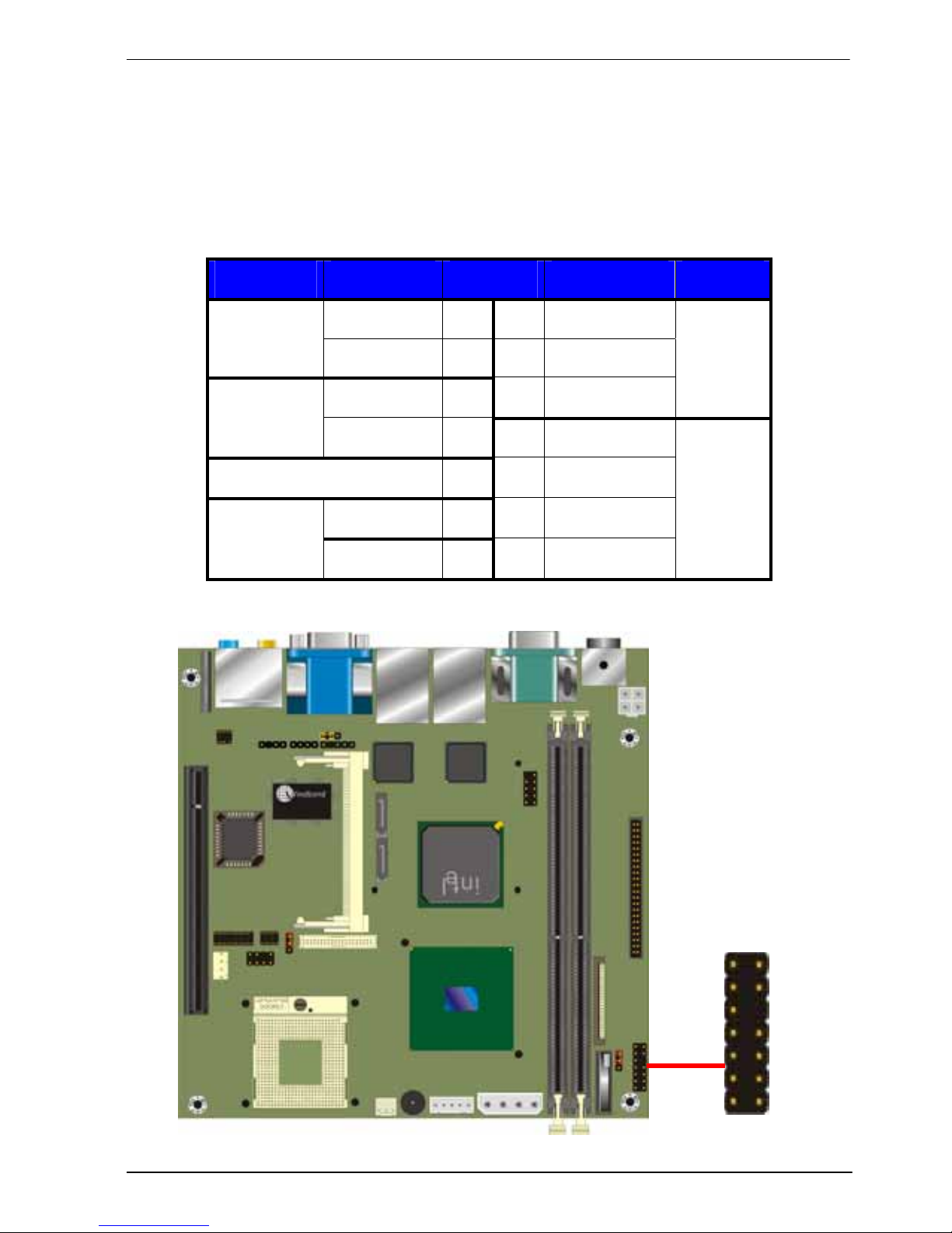
2.14 <Switch and Indicator>
The JFRNT provides front control panel of the board, such as p ower button, reset and
beeper, etc. Please check well before you connecting the cables on the chassis.
Connector: JFRNT
Type: onboard 14-pin (2 x 7) 2.54-pitch header
Function Signal PIN Signal Function
VCC 1 2 VCC
IDE LED
Active 3 4 N/C
Reset 5 6 GND
Power
LED
Reset
GND 7 8 VCC
N/C 9 10 N/C
PWRBT 11 12 N/C
Power
Button
5VSB 13 14 SPKIN
Speaker
1
14
JFRNT
Page 34
LV-673(E) User’s Manual Hardware Setup
Power Supply
34
Chapter 3 <System Setup>
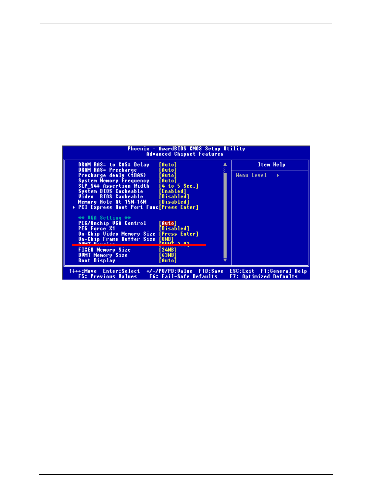
3.1 <Video Memory Setup>
Based on Intel® 915GM(E) chipset with GMA (Graphic Media Accelerator) 900, the
board supports Intel® DVMT (Dynamic Video Memory Technology) 3.0, which would
allow the video memory to be allocated up to 128MB.
To support DVMT, you need to install the Intel GMA 900 Driver with supported OS.
BIOS Setup:
On-Chip Video Memory Size: This option combines three items below for setup.
On-Chip Frame Buffer Size:
This item can let you select video memory which been allocated for legacy VGA and
SVGA graphics support and compatibility. The available option is 1MB and 8MB.
Fixed Memory Size:
This item can let you select a static amount of page-locked graphics memory which will
be allocated during driver initialization. Once you select the memory amount, it will be no
longer available for system memory.
DVMT Memory Size:
This item can let you select a maximum size of dynamic amount usage of video memory,
the system would configure the video memory depends on your applic ation, this item is
strongly recommend to be selected as MAX DVMT.
Page 35
LV-673(E) User’s Manual System Setup
Video Memory Setup
35
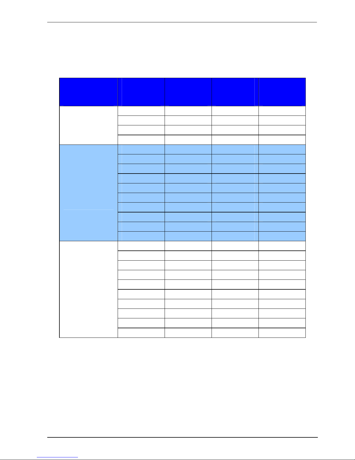
Fixed + DVMT Memory Size:
You can select the fixed amount and the DVMT amount at the same time for a
guaranteed video memory and additional dynamic video memory, please check the
table below for available setting.
System
Memory
On-Chip
Frame
Buffer Size
Fixed
Memory
Size
DVMT
Memory
Size
Total
Graphic
Memory
1MB 32MB 0MB 32MB
1MB 0MB 32MB 32MB
8MB 32MB 0MB 32MB
128MB~255MB
8MB 0 32MB 32MB
1MB 64MB 0MB 64MB
1MB 0 64MB 64MB
1MB 128MB 0MB 128MB
1MB 0 128MB 128MB
1MB 64MB 64MB 128MB
8MB 64MB 0MB 64MB
8MB 0 64MB 64MB
8MB 128MB 0MB 128MB
8MB 0 128MB 128MB
256MB~511MB
8MB 64MB 64MB 128MB
1MB 64MB 0 64MB
1MB 0 64MB 64MB
1MB 128MB 0 128MB
1MB 0 128MB 128MB
1MB 64MB 64MB 128MB
8MB 64MB 0 64MB
8MB 0 64MB 64MB
8MB 128MB 0 128MB
8MB 0 128MB 128MB
512MB upper
8MB 64MB 64MB 128MB
Notice:
1. The On-Chip Frame Buffer Size would be included in the Fixed Memory.
Please select the memory size according to this table.
Page 36
LV-673(E) User’s Manual System Setup
Video Memory Setup
36
Chapter 4 <BIOS Setup>
The motherboard uses the Award BIOS for the system configuration. The Award BIOS
in the single board computer is a customized version of the i ndustri al standard BIOS for
IBM PC AT-compatible computers. It supports Intel x86 and compatible CPU
architecture based processors and computers. The BIOS provides critical low-level
support for the system central processing, memory and I/O sub-systems.
The BIOS setup program of the single board computer let the customers modify the
basic configuration setting. The settings are stored in a dedicated battery-backed
memory, NVRAM, retains the information when the power is turned off. If the battery
runs out of the power, then the settings of BIOS will come back to the default setting.
The BIOS section of the manual is subject to change without notice and is provided here
for reference purpose only. The settings and configuration s of the BIOS are current at
the time of print, and therefore they may not be exactly the same as that displayed on
your screen.
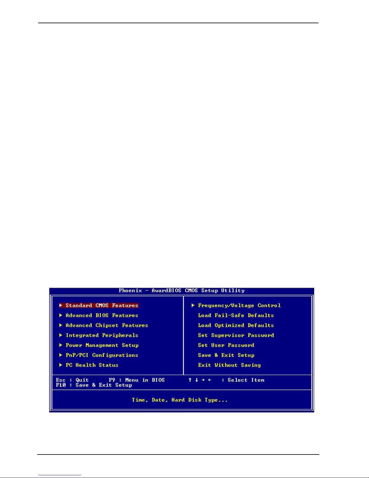
To activate CMOS Setup program, press <DEL> key i mmediately after you turn on
the system. The following message “Press DEL to enter SETUP” should appear in th e
lower left hand corner of your screen. When you enter the CMOS Setup Utility, the Main
Menu will be displayed as Figure 4-1. You can use arrow keys to select your function,
press <Enter> key to accept the selection and enter the sub-menu.
Figure 4-1 CMOS Setup Utility Main Screen
Page 37

LV-673(E) User’s Manual BIOS Setup
BIOS Setup
37
(This Page is Left for Blank)
Page 38
LV-673(E) User’s Manual
38
Appendix A <I/O Port Pin Assignment>
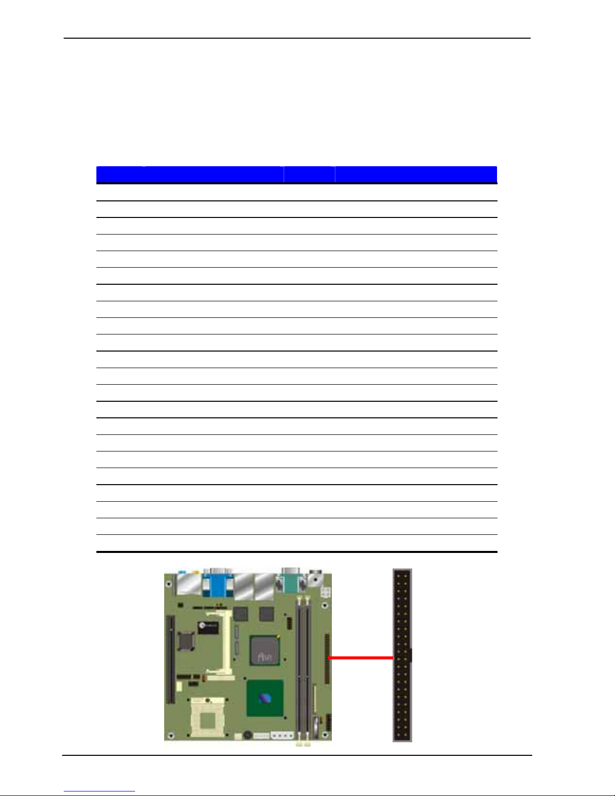
A.1 <IDE Port>
Connector: IDE1
Type: 44-pin (22 x 2) box header
Pin Description Pin Description
1 Reset 2 Ground
3 D7 4 D8
5 D6 6 D9
7 D5 8 D10
9 D4 10 D11
11 D3 12 D12
13 D2 14 D13
15 D1 16 D14
17 D0 18 D15
19 Ground 20 N/C
21 REQ 22 Ground
23 -IOW 24 Ground
25 -IOR 26 Ground
27 IORDY 28 Ground
29 DACK 30 Ground
31 IDEIRQ 32 IDE32
33 A1 34 P66DET
35 A0 36 A2
37 -CS1 38 -CS3
39 -HD LED1 40 Ground
41 +5V 42 +5V
43 Ground 44 Ground
1
2
4344
Page 39
LV-673(E) User’s Manual I/O Port Pin Assignment
IDE Port
39
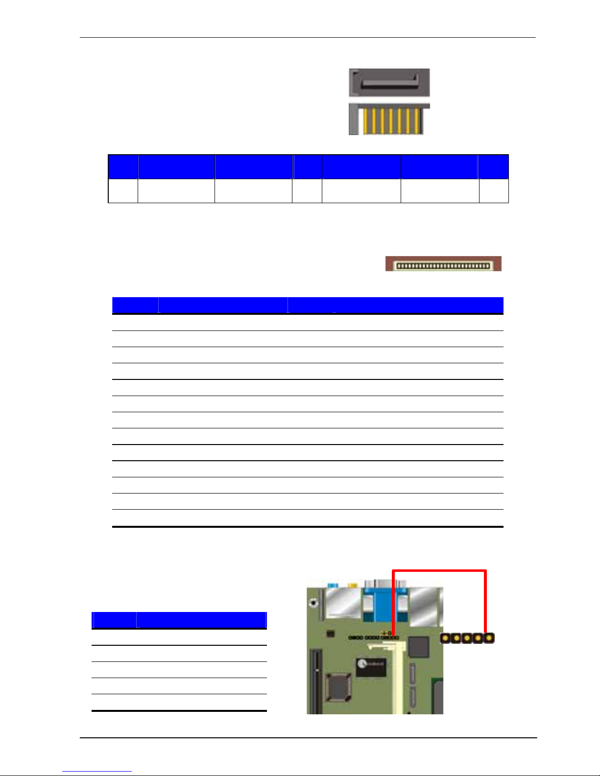
A.2 <Serial ATA Port>
Connector: SATA1/2
Type: 7-pin wafer connector
1 2 3 4 5 6 7
GND RSATA_TXP1 RSATA_T XN1 GND RSATA_RXN1 RSATA_RXP1 GND
A.3 <Floppy Port>
Connector: FDD
Type: 26-pin connector
Pin Description Pin Description
1 VCC 2 INDEX
3 VCC 4 DRV0
5 VCC 6 DSKCHG
7 DRV1 8 N/C
9 MTR1 10 MTR0
11 RPM 12 DIR
13 N/C 14 STEP
15 Ground 16 WRITE DATA
17 Ground 18 WRITE GATE
19 N/C 20 TRACK 0
21 N/C 22 WRPTR
23 Ground 24 RDATA25 Ground 26 SEL
A.4 <IrDA Port>
Connector: CN_IR
Type: 5-pin header for SIR Ports
Pin Description
1 VCC
2 N/C
3 IRRX
4 Ground
5 IRTX
1
Page 40
LV-673(E) User’s Manual System Resources
Serial ATA Port
40
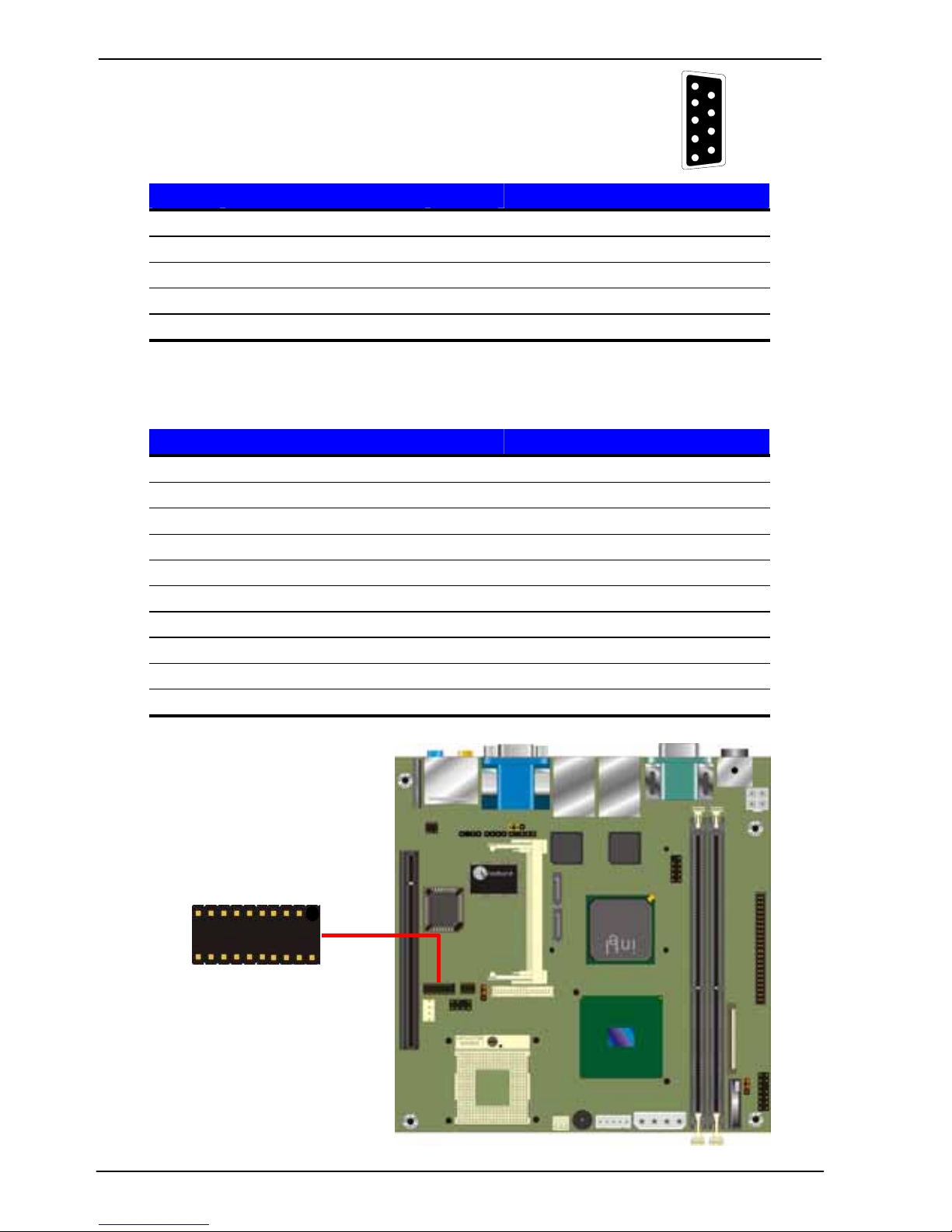
A.5 <Serial Port>
Connector: COM1/COM2
Type: 9-pin D-sub male connector on bracket
Pin Description Pin Description
1 DCD 6 DSR
2 SIN 7 RTS
3 SO 8 CTS
4 DTR 9 RI
5 Ground
Connector: CN_COM34
Type: 20-pin (10 x 2) 1.27mm x 2.54mm-pitch header
Pin Description Pin Description
1 DCD 2 RXD
3 TXD 4 DTR
5 GND 6 DSR
7 RTS 8 CTS
9 RI 10 N/C
11 DCD 12 RXD
13 TXD 14 DTR
15 GND 16 DSR
17 RTS 18 CTS
19 RI 20 N/C
1
2
3
4
5
6
7
8
9
1
2
19
20
Page 41
LV-673(E) User’s Manual I/O Port Pin Assignment
Serial Port
41
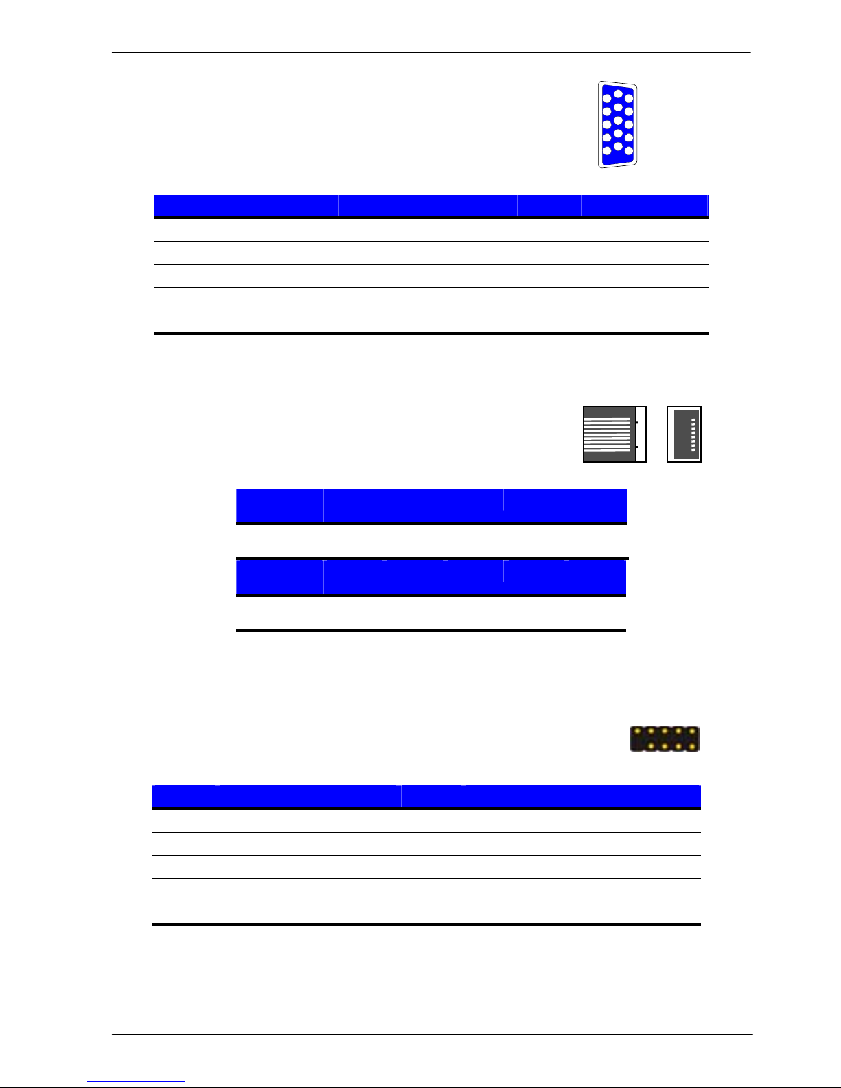
A.6 <VGA Port>
Connector: VGA
Type: 15-pin D-sub female connector on bracket
Pin Description Pin Description Pin Description
1 RED 6 Ground 11 N/C
2 GREEN 7 Ground 12 VCC
3 BLUE 8 Ground 13 HSYNC
4 N/C 9 N/C 14 VSYNC
5 Ground 10 Ground 15 5VCLK
A.7 <LAN Port>
Connector: RJ451/2
Type: RJ45 connector with LED on bracket
Pin 1 2 3 4 5
Description TRD0+ TRD0- TRD1+ TRD1- NC
Pin 6 7 8 9 10
Description NC TRD2+ TRD2- TRD3+ TRD3-
A.8 < USB Interface >
Connector: CN_USB
Type: 10-pin (5 x 2) header for dual USB Ports
Pin Description Pin Description
1 VCC 2 VCC
3 Data0- 4 Data15 Data0+ 6 Data1+
7 Ground 8 Ground
9 Ground 10 NC
6
10
1
2
3
4
5
11
12
13
14
15
1
10
2
9
Page 42

LV-673(E) User’s Manual System Resources
Watchdog Timer Setting
42
Appendix B <Flash BIOS>
B.1 <Flash Tool>
The board is based on Award BIOS and can be updated easily by the BIOS auto
flash tool. You can download the tool online at the address below:
http://www.phoenix.com/en/home/
http://www.commell.com.tw/Support/Support_SBC.htm
File name of the tool is “awdflash.exe”, it’s the utility that can write the data into the
BIOS flash ship and update the BIOS.
B.2 <Flash BIOS Procedure>
1. Please make a bootable floppy disk.
2. Get the last .bin files you want to update and copy it into the disk.
3. Copy awardflash.exe to the disk.
4. Power on the system and flash the BIOS. (Example: C:/ awardflash XXX.bin)
5. Restart the system.
Any question about the BIOS re-flash please contact your distributors or visit the
web-site at below:
http://www.commell.com.tw/support/support.htm
UT
Page 43
LV-673(E) User’s Manual
43
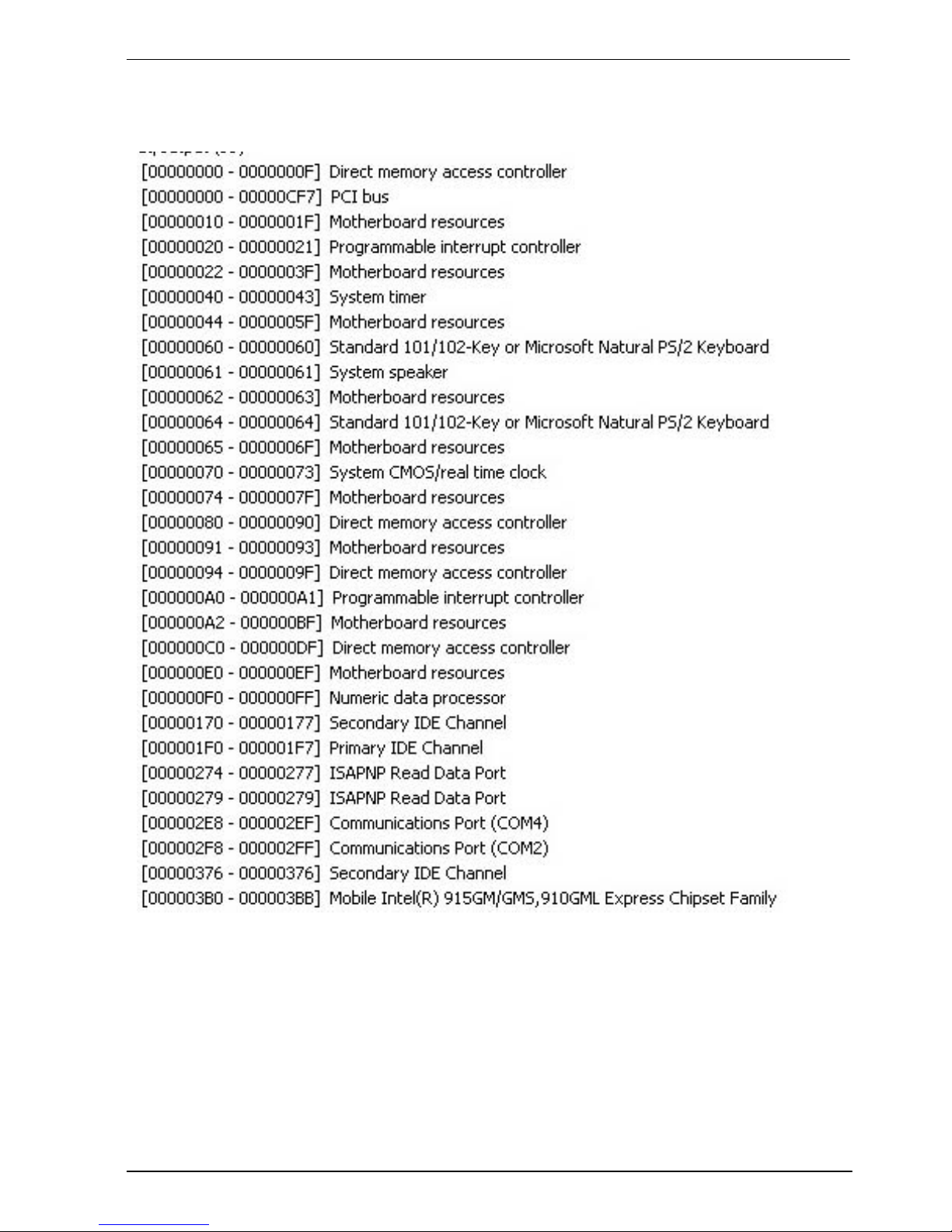
Appendix C <System Resources>
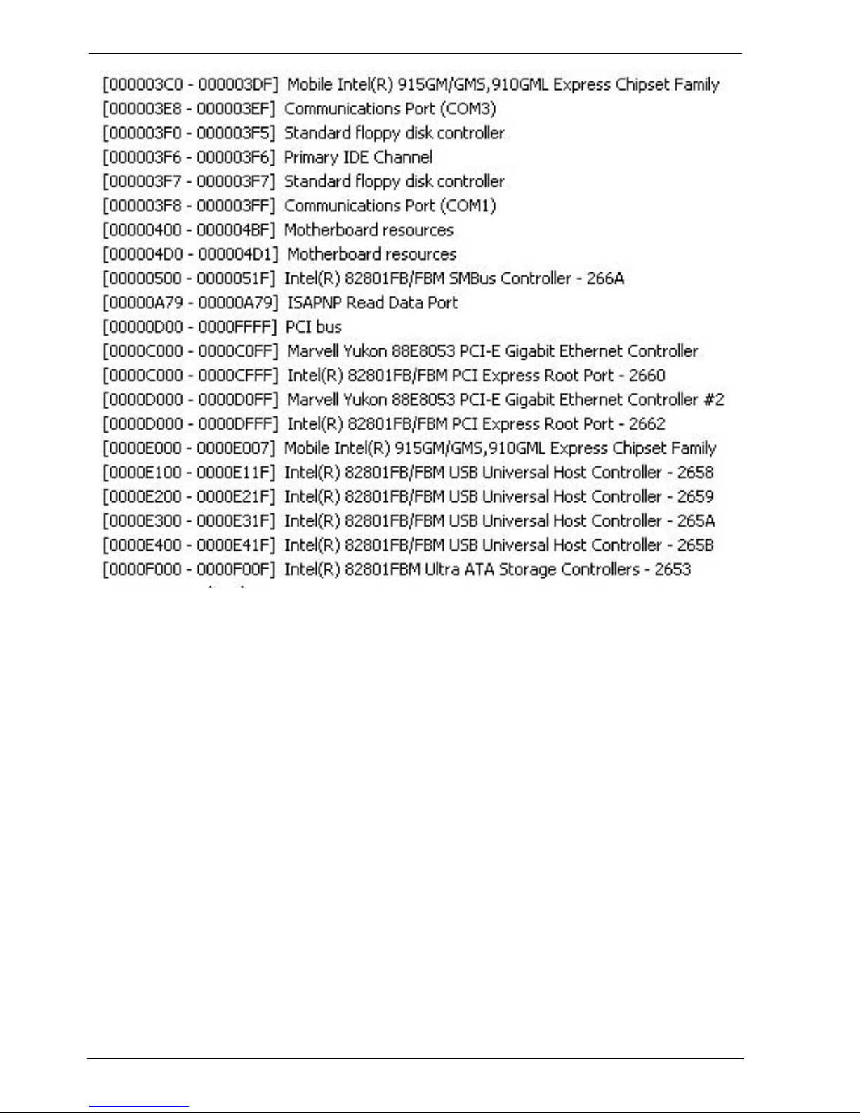
C1. <I/O Port Address Map>
Page 44
LV-673(E) User’s Manual System Resources
Watchdog Timer Setting
44
Page 45
LV-673(E) User’s Manual
45
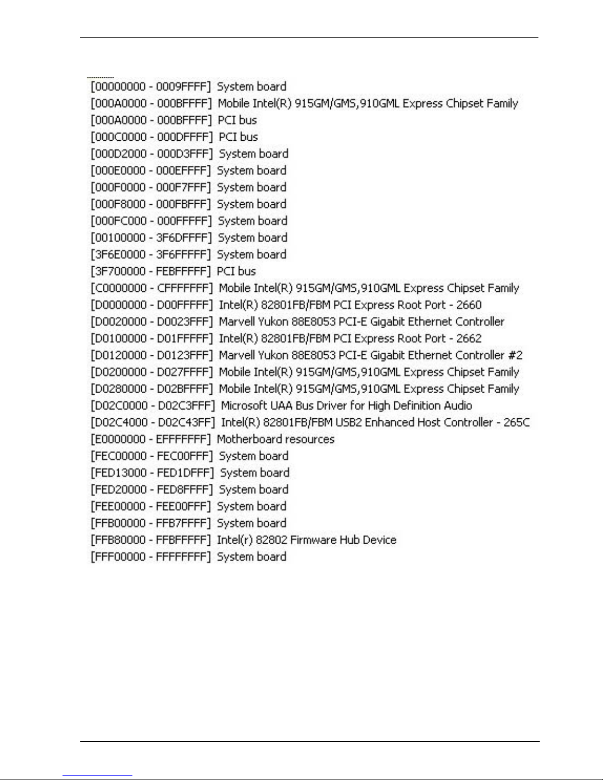
C2. <Memory Address Map>
Page 46
LV-673(E) User’s Manual System Resources
Watchdog Timer Setting
46
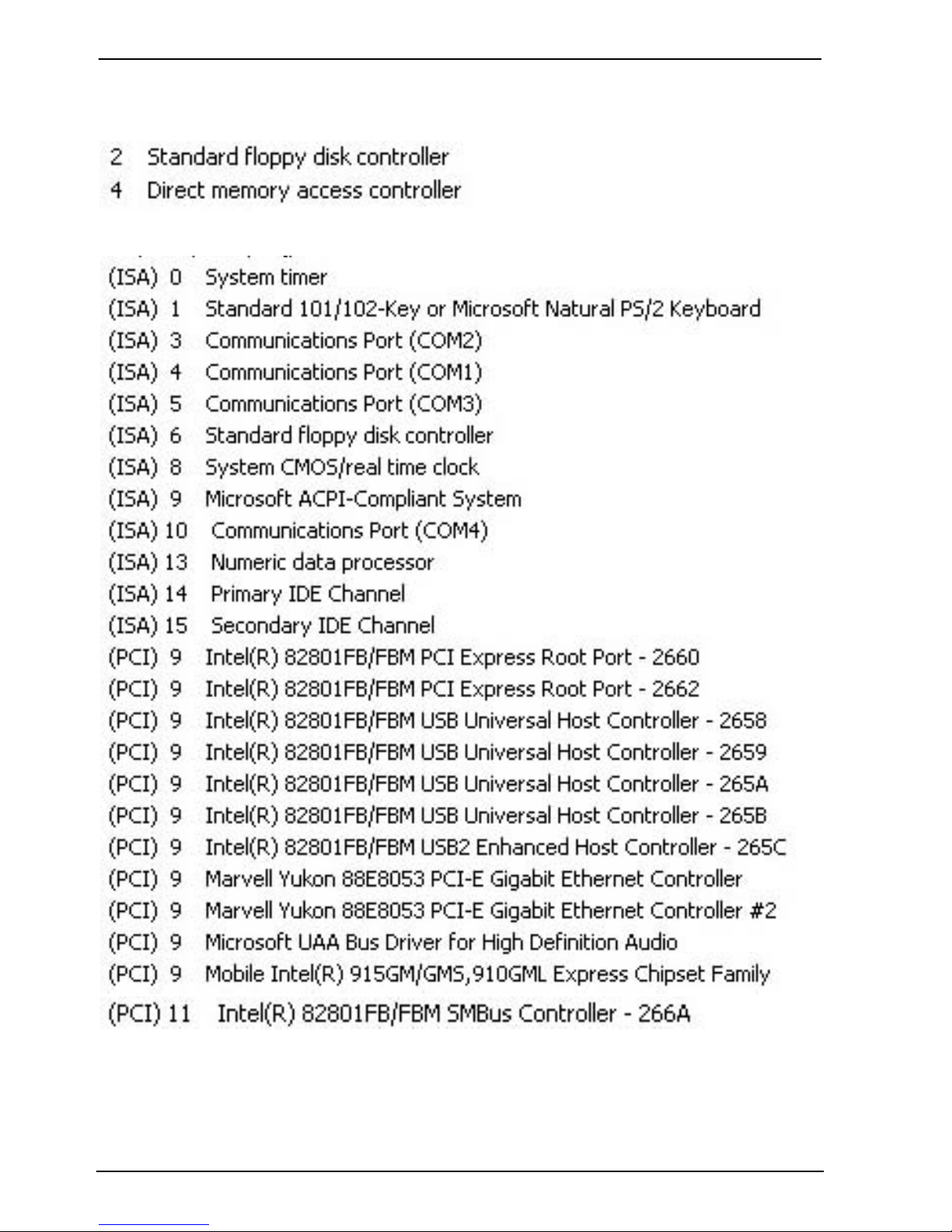
C3. <System IRQ & DMA Resources>
DMA:
IRQ:
Page 47

LV-673(E) User’s Manual
47
C4. <GPIO programmed>
The GPIO’can be programmed with the MSDOS debug program using simple
IN/OUT commands.The following lines show an example how to do this.
GPIO0…..GPIO7 bit0……bit7
-o 4E 87 ;enter configuration
-o 4E 87
-o 4E 29
-o 4E 40 ;enale GPIO function
-o 4E 07
-o 4E 07 ;enable GPIO configuration
-o 4E F0
-o 4F xx ;set GPIO as input/output; set ‘1’ for input,’0’for output
-o 4E F1
-o 4F xx ;if set GPIO’s as output,in this register its value can be set
Optional :
-o 4E F2
-o 4F xx ; Data inversion register ; ‘1’ inverts the current valus of the
bits ,’0’ leaves them as they are
-o 4E 30
-o 4F 01 ; active GPIO’s
For further information ,please refer to Winbond W83627THF datasheet.
Page 48

LV-673(E) User’s Manual System Resources
Watchdog Timer Setting
48
C5. <Watchdog Timer Setting>
The watchdog timer makes the system auto-reset while it stops to work for a period. The
integrated watchdog timer can be setup as system reset mode by program.
Timeout Value Range
- 1 to 255
- Second or Minute
Program Sample
Watchdog timer setup as system reset with 5 second of timeout
-o 4E 87 ;enter configuration
-o 4E 87
-o 4E 07
-o 4F 08 ;enter Logical Device 8
-o 4E F5
-o 4F 00 ;set as Second* Minute: bit 3 = 1; Second: bit 3 = 0
-o 4E F6
-o 4F 05 ;set as 5 Second
Page 49

LV-673(E) User’s Manual
49
Contact Information
Any advice or comment about our products and service, or
anything we can help you please don’t hesitate to contact with us.
We will do our best to support you for your products, projects a
business.
Taiwan Commate Computer Inc.
Address
19F, No. 94, Sec. 1, Shin Tai Wu Rd., Shi Chih
Taipei Hsien, Taiwan
TEL +886-2-26963909
FAX +886-2-26963911
Website
TUhttp://www.commell.com.twUT
E-Mail
Commell is our trademark of industrial PC division
 Loading...