

Page 1
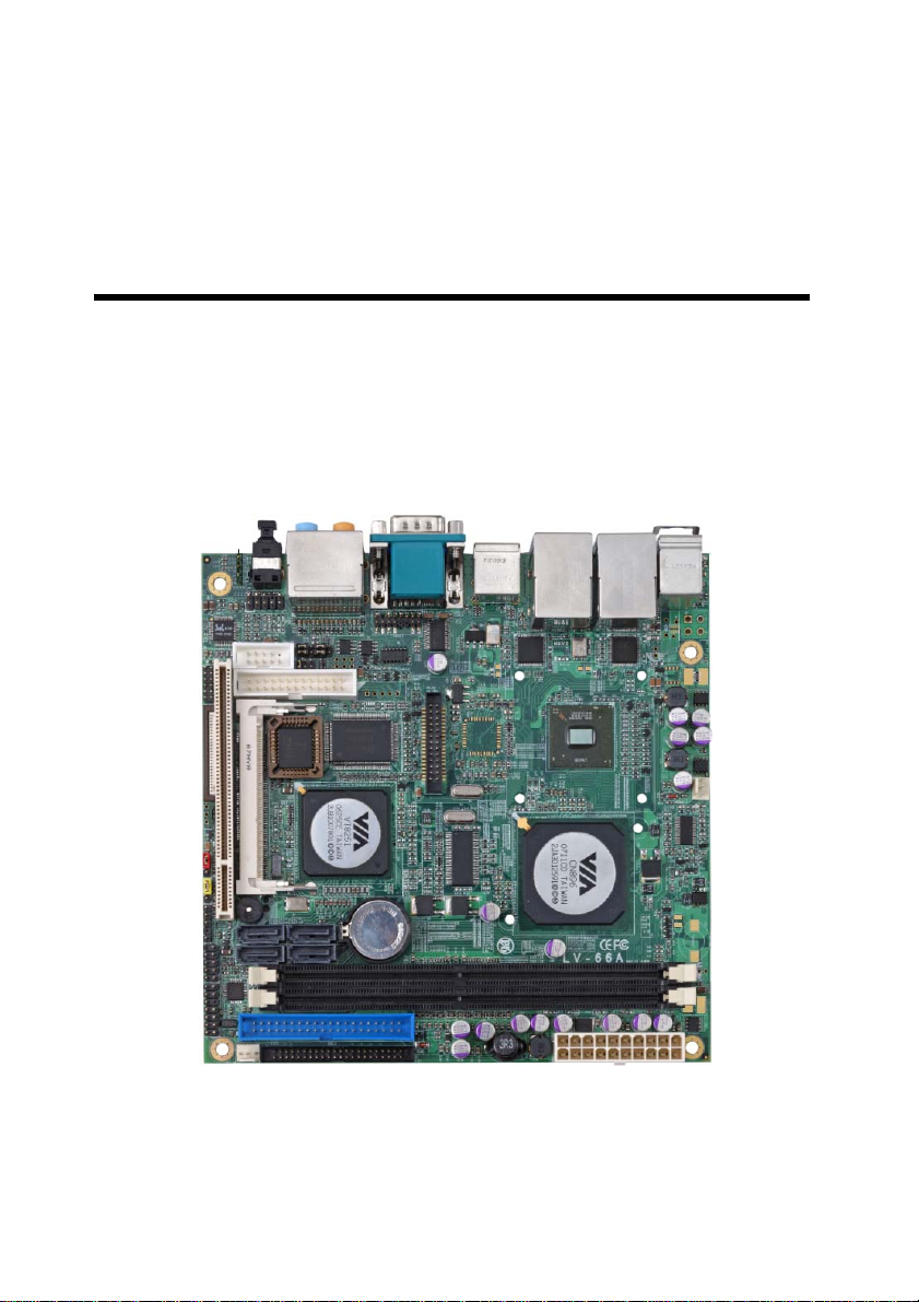
LV-66A
Mini-ITX Motherboard
User’s Manual
Edition 1.02
2009/02/17
Page 2

LV-66A User’s Manual
Copyright
Copyright 2008. All rights reserved. This document is copyrighted and all rights are
reserved. The information in this document is subject to change without prior notice to make
improvements to the products.
This document contains proprietary information and protect ed by copyright. No part of this
document may be reproduced, copied, or translated in any form or any means without prior
written permission of the manufacturer.
All trademarks and/or registered trademarks contains in this document are propert y of their
respective owners.
Disclaimer
The company shall not be liable for any incidental or consequenti al dam ages res ultin g from
the performance or use of this product.
The company does not issue a warranty of any kind, e xpress or implied, including without
limitation implied warranties of merchantability or fitness for a particular purpose.
The company has the right to revise the manual or include changes in th e specifications of
the product described within it at any time without notice and without obligation to notify any
person of such revision or changes.
Trademark
All trademarks are the property of their respective holders.
Any questions please visit our website at TUhttp://www.commell.com.twUT
2
Page 3
LV-66A User’s Manual
Packing List
Please check the package before you starting setup the system
Hardware:
LV-66A series motherboard x 1
Cable Kit:
44-pin ATA33 IDE Cable x 1
26-pin Slim Type Floppy Cable x 1
DVI module with DVI Cable x 1
(LV-66AD series only)
I/O Shield x 1
40-pin ATA100 IDE Cable x 1
Printer Port Cable & COM Port Cable x 1
SATA Cable x 2
Printed Matters:
Driver CD x 1 (Including User’s Manual)
3
Page 4

LV-66A User’s Manual
Index
Chapter 1 <Introduction>
1.1 <Product Overview>.................................................................................7
1.2 <Product Specification>...........................................................................8
1.3 <Mechanical Drawing>...........................................................................10
1.4 <Block Diagram>....................................................................................11
....................................................................7
Chapter 2 <Hardware Setup>.........................................................12
2.1 <Connector Location>............................................................................12
2.2 <Jumper Reference> .............................................................................14
2.3 <Connector Reference>.........................................................................15
2.3.1 <Internal Connector>..................................................................15
2.3.2 <External Connector>.................................................................15
2.4 <CPU and Memory Setup>.................................................................... 16
2.4.1<CPU>.........................................................................................16
2.4.2 <Memory> ..................................................................................16
2.5 <CMOS & AT/ATX Setup>.....................................................................17
2.6 <Solid State Disk Interface>...................................................................18
2.7 <Serial ATA Interface>...........................................................................19
2.8 <Floppy Port>......................................................................................... 20
2.9 <LAN Interface>.....................................................................................21
2.10 <Onboard Display Interface>...............................................................22
2.10.1 <Analog VGA Interface> ..........................................................22
2.10.2 <Digital Display>.......................................................................23
2.10.2.1 <LVDS Display> .............................................................23
2.10.2.2 <DVI Display> ................................................................27
2.11 <Onboard Audio Interface>..................................................................28
2.12 <USB2.0 Interface>..............................................................................29
2.13 <GPIO Interface>.................................................................................31
4
Page 5

LV-66A User’s Manual
2.14 <Serial Port Jumper Setting >..............................................................32
2.15 <Fan Connector>.................................................................................34
2.16 <Indicator and Switch>.........................................................................35
2.17 <Power Supply>...................................................................................36
2.17.1 <DC_IN Input>..........................................................................36
2.17.2 <ATX Input> .............................................................................37
Chapter 3 <System Configuration>...........................................39
3.1 <SATA RAID Configuration>..................................................................39
3.2 <Audio Configuration> ...........................................................................42
3.3 <Display Configuration>.........................................................................43
Chapter 4 <BIOS Setup>....................................................................47
Appendix A <I/O Port Pin Assignment>................................. 49
A.1 <IDE Port>.............................................................................................49
A.2 <Floppy Port> ........................................................................................ 51
A.3 <Serial ATA Port>..................................................................................51
A.4 < CRT Port >..........................................................................................52
A.5 <Serial Port>..........................................................................................52
A.6 <LAN Port>............................................................................................52
Appendix B <Flash BIOS>................................................................53
B.1 BIOS Auto Flash Tool .....................................................................53
B.2 Flash Method...................................................................................53
Appendix C <System Resources>............................................. 54
C1.<I/O Port Address Map>................................................................54
C2.<Memory Address Map>................................................................56
C3.<System IRQ Resources>.............................................................58
Appendix D <Programming GPIO’s>.......................................59
Appendix E <Watch Dog timer Setting >............................... 61
Contact Information..............................................................................63
5
Page 6

LV-66A User’s Manual
(The Page is Left For Blank)
6
Page 7

LV-66A User’s Manual Introduction
Chapter 1 <Introduction>
1.1 <Product Overview>
LV-66A is the Mini-ITX motherboard based on VIA chipset. It integrates VIA embedded
chipset for CN896 with VT8251, two DDR2 400/533/667 SDRAM 64-bit single channel, and
serial ATA II supporting 1.5 Gbit/s and 3 Gbit/s transfer rate with RAID 0/1/0+1/5 and JBOD
array Technology supported to provide the economical embedded platform.
VIA CN896 & VT8251 Chipset
The board comes with the VIA embedded chipset of CN896, supports two DDR2
400/533/667 SDRAM, Chrome9™ HC Integrated Graphics with 2D / 3D / Video Controllers,
The VT8251 provides the board to support Ultra V-Link interface with 1 GB/sec maximum
bandwidth, four serial ATA II ports with RAID array function, 8 x USB2.0 ports and 7.1
channels HD audio.
Multimedia solution
Based on VIA CN896 chipset, the board provides single/dual 18/24-bit LVDS or DVI
interface, which supports dual independent display with CRT.
Onboard HD codec provides the high quality of sound including 7.1-channel stereo DACs.
Two LAN Interface
LV-66A also comes with two Giga LAN interface, support boot-on-LAN and wake-on-LAN
function.
High Speed Hot-plug Interface
Based on VIA VT8251 the board provides 8 USB2.0 interfaces with up to 480Mbps of
transferring rate.
7
Page 8

LV-66A User’s Manual Introduction
1.2 <Product Specification>
General Specification
Form Factor Mini-ITX motherboard
CPU VIA C7 1.5GHz processor
L1/L2 Cache: 64 KB/128KB
Front side bus: 400MHz
Memory 2 x 240-pin DDR2 400/533/667 SDRAM up to 4GB Advanced 64-bit
single channel,
Unbufferred, non-ECC memory supported only
Chipset VIA CN896 and VT8251
BIOS Phoenix-Award v6.00PG 4Mb PnP flash BIOS
Green Function Power saving mode includes doze, standby and suspend modes. ACPI
version 1.0 and APM version 1.2 compliant
Watchdog Timer System reset programmable watchdog timer with 1 ~ 255 sec./min. of
timeout value
Real Time Clock VIA VT8251 built-in RTC with lithium battery
Enhanced IDE Enhanced IDE interface supports dual channels and up to 4 ATAPI
devices
One 40-pin and one 44-pin IDE port onboard
Solid State Disk One Compact Flash Type II (Optional)
Serial ATA VIA VT8251 integrates 4 Serial ATA II interface supporting 1.5 Gbit/s and 3
Gbit/s transfer rate
RAID 0/1/0+1/5 and JBOD array Technology supported
Multi-I/O Port
Chipset VIA VT8251 with Winbond W83697HG controller
Serial Port One RS-232 external & one internal RS-232/ RS-422/ RS-485 serial ports
USB Port Six external & two internal Hi-Speed USB 2.0 ports with 480Mbps of
transfer rate
Parallel Port One 26-pin internal parallel port
Floppy Port One slim type Floppy port
K/B & Mouse PS/2 keyboard and mouse
GPIO One 12-pin Digital I/O connector with 8-bit programmable I/O interface
Hardware Monitor Fan speed, CPU temperature and voltage monitoring
VGA Display Interface
Chipset VIA CN896 Integrated Chrome9™ HC IGP & Video Controller
Core Frequency 250MHz
Memory BIOS selectable 64/128/256MB shard with system memory
Display Type CRT, LCD monitor with analog display
onboard 18/24-bit single/dual LVDS or DVI
8
Page 9

LV-66A User’s Manual Hardware Setup
Connector External DB15 female VGA connector on rear I/O panel
Onboard 40-Pin LVDS connector(LV-66AX series only)
Onboard 26-Pin DVI connector(LV-66AD series only)
Ethernet Interface
Chipset REALTEK RTL8111C
Type Integrated 10/100/1000 transceiver
auto-switching Fast Ethernet
Full Duplex flow control (IEEE 802.3x), Fully compliant with IEEE 802.3,
IEEE 802.3u, IEEE 802.3ab
Connector Two External RJ45 connectors with LED on rear I/O panel
Audio Interface
Chipset REALTEK ALC888
Interface 7.1 channel surround audio with Line-out and MIC-in
Connector Onboard audio connector with pin header and phone jack
Onboard CD-IN connector
Expansive Interface
PCI 1 x PCI slot supports up to two PCI devices through riser card
Mini PCI 1 x Mini PCI socket support Mini PCI type II
Power and Environment
Power
Requirement
Dimension 170 (L) x 170 (H) mm
Temperature Operating within 0 ~ 60℃ (32 ~ 140℉)
Standard 20-Pin ATX power supply
12V DC Input (Optional)
Storage within -20 ~ 85℃ (-4 ~ 185℉)
Ordering Code
LV-66A VIA C7 1.5G with Onboard VGA, AUDIO, 1XGiga LAN, USB2.0, COM,
FDD, LPT, GPIO, Mini PCI, SATA and SPDIF
LV-66AD VIA C7 1.5G with Onboard VGA, AUDIO, 2X Giga LAN, USB2.0, COM,
FDD, LPT, GPIO, Mini PCI, SATA, SPDIF and DVI
LV-66AX VIA C7 1.5G with Onboard VGA, AUDIO, 2X Giga LAN, USB2.0, COM,
FDD, LPT, GPIO, Mini PCI, SATA, SPDIF and LVDS
The specifications may be different as the actual production.
For further product information please visit the website at
TUhttp://www.commell.com.twUT
9
Page 10
LV-66A User’s Manual Introduction
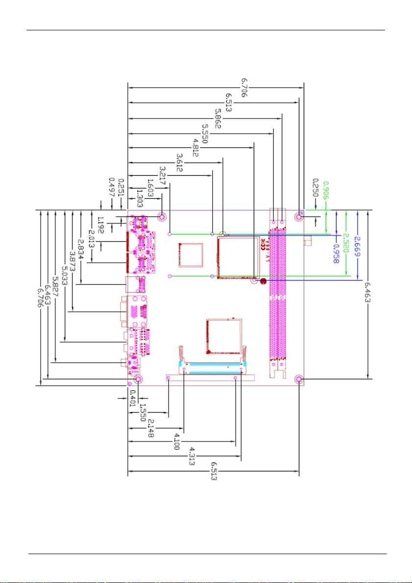
1.3 <Mechanical Drawing>
10
Page 11
LV-66A User’s Manual Hardware Setup
p
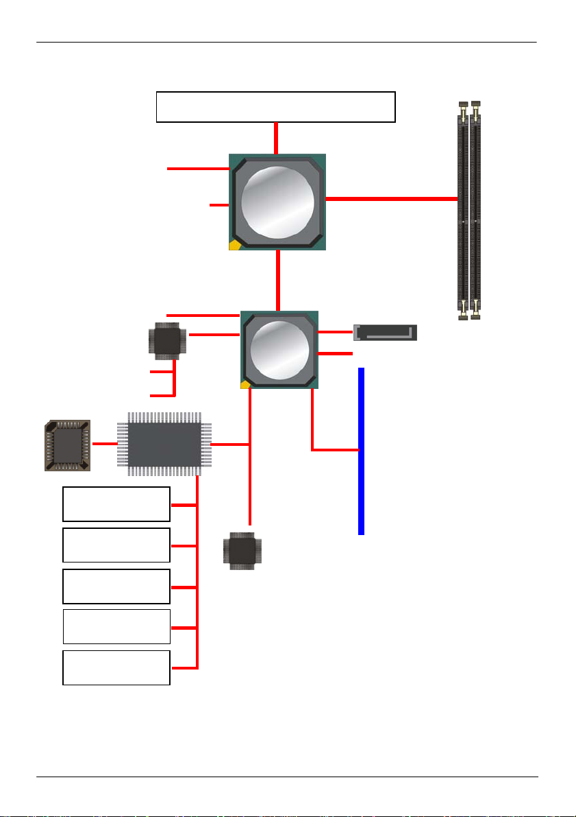
1.4 <Block Diagram>
C7 VIA nanoBGA2
CRT/LCD Monitor
VT1636 LVDS/VT1632A DVI
8 x USB2.0 Ports
HD ALC888
CDIN
SPDIF
BIOS
W83697HG
2 x Serial ports
1 x Floppy port
1 x IrDA
CN896
VT8251
2 x 8111C LAN
Ultra V-Link
533MB/s
2 x 240-pin DDR2
400/533/667
to 4GB
U
4 x SATA
40-Pin 44-Pin IDE
PCI
Mini PCI
1 x Parallel port
8-bit GPIO
11
Page 12
LV-66A User’s Manual Hardware Setup
Chapter 2 <Hardware Setup>
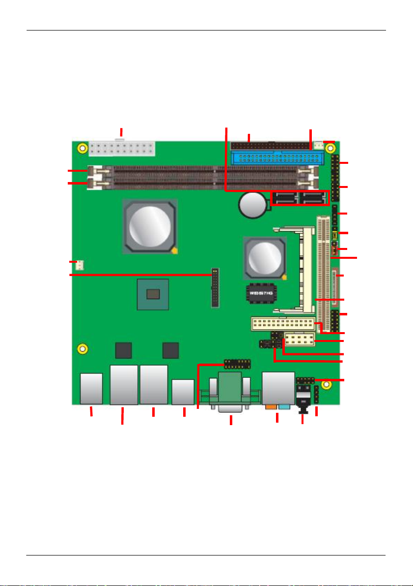
2.1 <Connector Location>
DDRIIB
DDRIIA
CPUFAN
CN_DVI/
CN_LVDS
ATX
SATA2/4
SATA1/3
IDE2
IDE1
SYSFAN
JFRNT
CN_FUSB
CN_IR
JAT
JRTC
PCI
FDD
MINIPCI
CN_DIO
CN_LPT
CN_COM2
JCSEL2
JCSEL1
CN_FAUDIO
PS2
USB-RJ45_2
USB-RJ45_1
CN_CRT
USB
CRT+COM
AUDIO
CDIN
SPDIF
12
Page 13
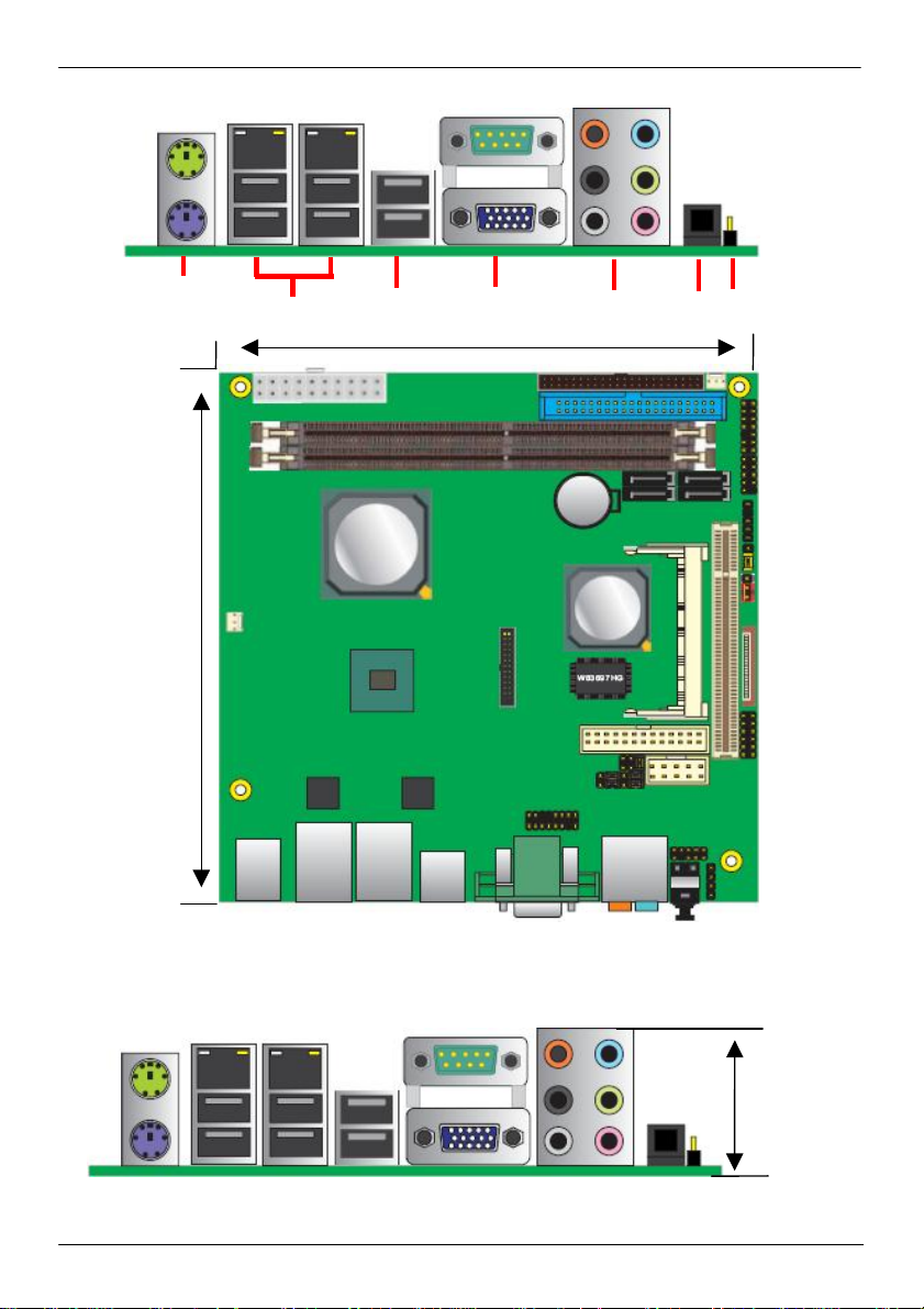
LV-66A User’s Manual Hardware Setup
PS2
USB_RJ45_1/2
USB
CRT+COM
170mm
AUDIO
SPDIF CDIN
170mm
14.25’
13
Page 14
LV-66A User’s Manual Hardware Setup
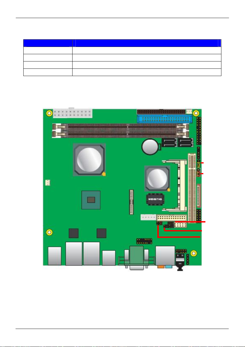
2.2 <Jumper Reference>
Jumper Function
JRTC CMOS Operating/Clear Setting
JVLCD LCD Panel Voltage Setting (LV-66AX series only)
JAT AT/ATX mode setting
JCSEL1/2 CN_COM2 RS232/422/485 mode setting
JAT
JRTC
JCSEL2
JCSEL1
JVLCD
14
Page 15
LV-66A User’s Manual Hardware Setup
2.3 <Connector Reference>
2.3.1 <Internal Connector>
Connector Function Remark
DDRIIA&DDRIIB 240-pin DDR2 SDRAM DIMM Standard
IDE1 40-pin primary IDE connector Standard
IDE2 44-pin secondary IDE connector Slim
FDD 26-pin slim type floppy connector Slim
SATA1/2/3/4 7-pin Serial ATA connector Standard
CN_FAUDIO 5 x 2-pin audio connector Standard
CDIN 4-pin CD-ROM audio input connector Standard
CN_DIO 6 x 2-pin digital I/O connector Standard
CN_FUSB 5 x 2-pin USB connector Standard
CPUFAN 3-pin CPU cooler fan connector Standard
SYSFAN 3-pin system cooler fan connector Standard
CN_COM2 5 x 2-pin RS232 serial port Standard
CN_LVDS 20 x 2-pin LVDS LCD interface(LV-66AX
series only)
CN_INV 5-pin LCD inverter connector (LV-66AX series
only)
JVLCD 3 x 2-pin LCD connector(LV-66AX series only) Standard
PCI Slim 32bit PCI slot Slim
MINIPCI Mini-PCI socket Standard
CN_LPT 13 x 2-pin printer connector Standard
CN_DVI 26-Pin connector(LV-66AD series only) Standard
JFRNT 14-pin switch/indicator connector Standard
CN_IR 5 x 1-pin IR connector Standard
Standard
Standard
2.3.2 <External Connector>
Connector Function Remark
CRT+COM DB15 VGA connector+ DB9 Serial port connector Standard
USB_RJ45_1&2 6 x USB and 2 x RJ45 LAN connector Standard
PS/2 PS/2 keyboard and mouse connector Standard
AUDIO 7.1 channel surround audio Standard
SPDIF SPDIF connector Standard
15
Page 16
LV-66A User’s Manual Hardware Setup
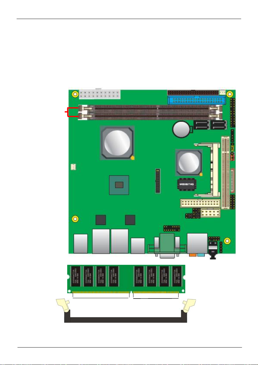
2.4 <CPU and Memory Setup>
2.4.1<CPU>
The board supports VIA C7 processor, default ratio is C7 1.5G 12W with cooler.
2.4.2 <Memory>
The board supports two 240-pin DDR2 400/533/667 SDRAM and up to 4GB Advanced
64-bit single channel, of capacity, only non-ECC, unbuffered memory is supported.
DDRIIA&DDRIIB
112-pin128-pin
Please check the pin number to match the socket side well
before installing memory module.
16
Page 17
LV-66A User’s Manual Hardware Setup
A
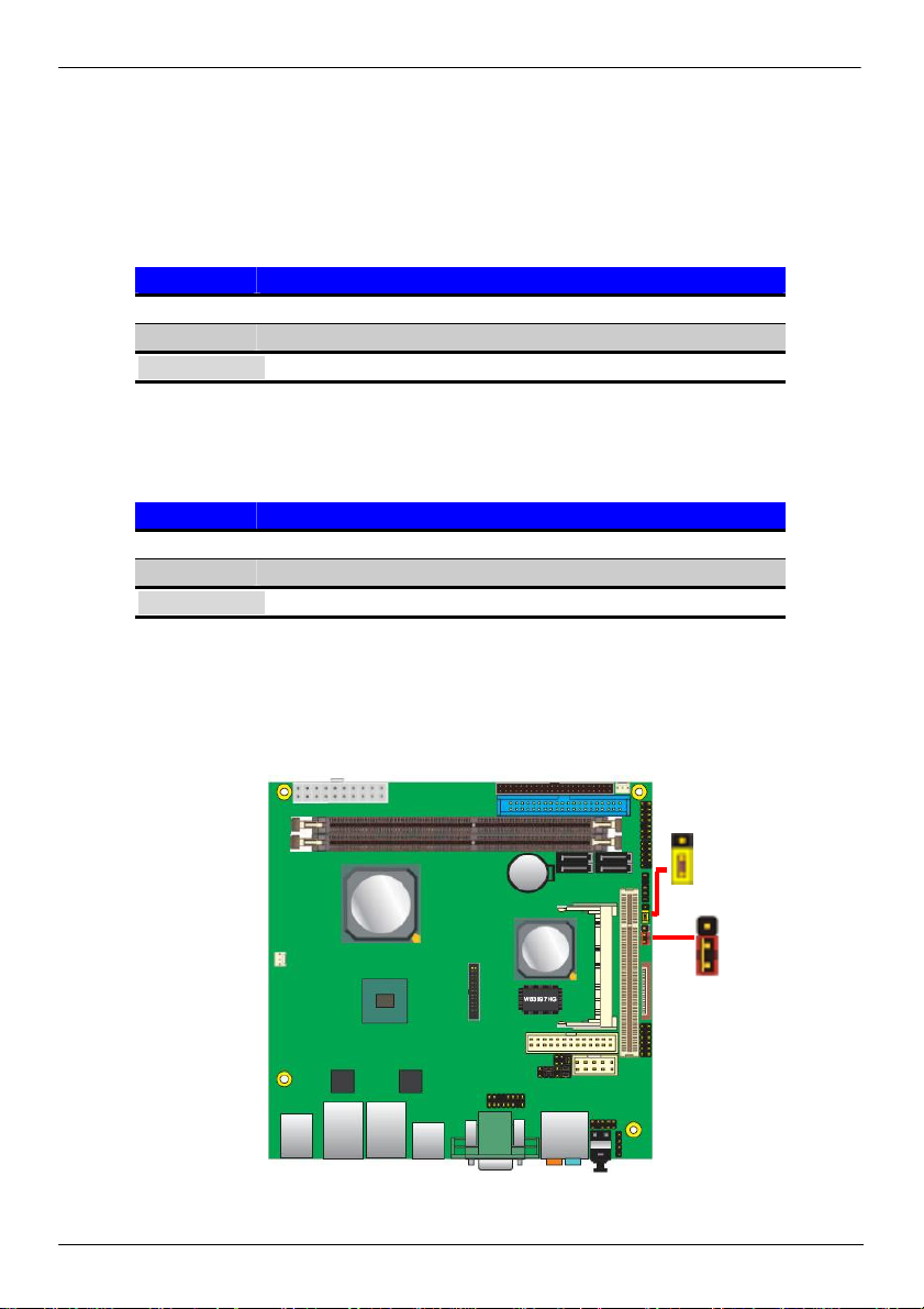
2.5 <CMOS & AT/ATX Setup>
The board’s data of CMOS can be setting in BIOS. If the board refuses to boot due to
inappropriate CMOS settings, here is how to proceed to clear (reset) the CMOS to its
default values.
Jumper: JRTC
Type: Onboard 3-pin jumper
JRTC Mode
1-2 Clear CMOS
2-3 Normal Operation
Default setting
Jumper: JAT
Type: Onboard 3-pin jumper
JAT Mode
1-2 AT mode
2-3 ATX mode
Default setting
1
J
T
3
1
JRTC
3
17
Page 18

LV-66A User’s Manual Hardware Setup
2.6 <Solid State Disk Interface>
The board has one Compact Flash Type II socket on the solder side, with jumper JCFSEL
for CF master/slave mode selection. (Optional)
Jumper: JCFSEL
Type: Onboard 3-pin jumper
JCFSEL Mode
1-2 Master mode
2-3 Slave mode
Default setting
1
JCFSEL
3
CF
18
Page 19
LV-66A User’s Manual Hardware Setup
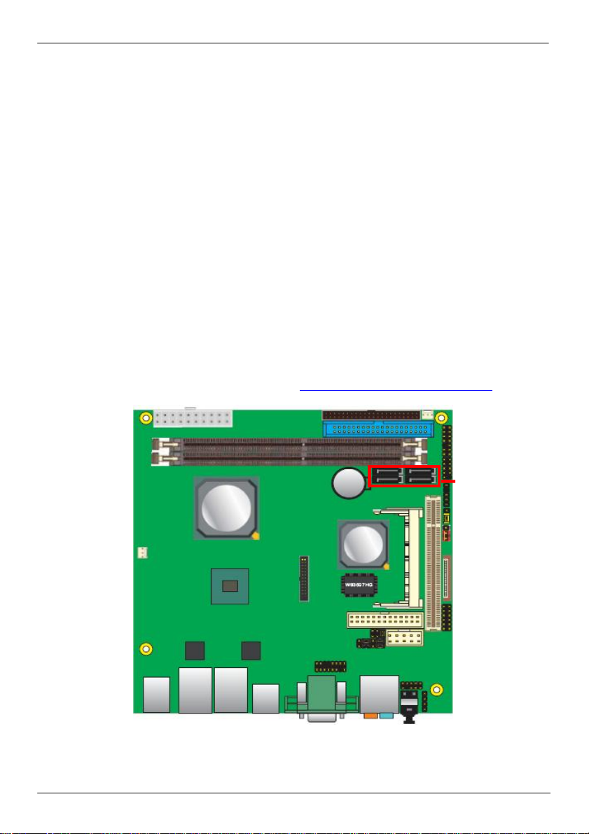
2.7 <Serial ATA Interface>
Based on VIA VT8251 Southbridge, the board supports four Serial ATA interfaces with
RAID array function. The following is the list of the specification of the Serial ATA.
1. Complies with Serial ATA Specification Revision 1.0
2. Complies with Serial ATA II Specification.
3. Supports up to 4 S-ATA devices: 4 SATA II AHCI Bus Masters or 2 SATA I Bus
Masters.
4. Integrated S-ATA PHY supporting 1.5 Gbit/s and 3 Gbit/s transfer rate.
5. Supports up to 32 entries command queue for each device.
6. Supports port multiplier.
7. Supports multiple RAID configurations - including RAID Level 0, RAID Level 1, RAID
Level 0+1, RAID Level 5 and JBOD.
For more information please visit VIA website (http://www.via.com.tw/en/index.jsp)
SATA2/4
SATA1/3
19
Page 20

LV-66A User’s Manual Hardware Setup
2.8 <Floppy Port>
The board provides a slim type floppy port; please use the 26-pin ribbon cable in the
package to connect the floppy device.
FDD
Floppy rear side
4. Lift up this plastic bar
5. Slot the cable in (Blue paste for outside)
6. Press back the plastic bar
1. Lift up the brown plastic bar
2. Slot the cable in (Blue paste for
brown bar side)
3. Press back the plastic bar
20
Page 21

LV-66A User’s Manual Hardware Setup
2.9 <LAN Interface>
The board provides two REALTEK RTL8111C GigaLAN interfaces and compliant. St andard
Integrated 10/100/1000 transceiver, auto-switching Fast Ethernet, Full Duplex flow control
(IEEE 802.3x), Fully compliant with IEEE 802.3, IEEE 802.3u, IEEE 802.3ab.
RJ45_1/2
21
Page 22

LV-66A User’s Manual Hardware Setup
2.10 <Onboard Display Interface>
Based on VIA CN896, the board supports Chrome9™ HC Integrated Graphics with 2D / 3D
/ Video Controllers, with BIOS selectable 64/128/256MB shared with system memory for
frame buffer.
2.10.1 <Analog VGA Interface>
The board provided a DB15 VGA connector on the rear I/O panel.
VGA
22
Page 23

LV-66A User’s Manual Hardware Setup
2.10.2 <Digital Display>
2.10.2.1 <LVDS Display>
The board provides one 40-pin LVDS connector for single/dual 18/24-bit channel panels,
supports up to 1920 x 1200 of resolution, with one LCD backlight inverter connector and
one jumper for panel voltage setting (LV-66AX series only)
1
5
2
6
JVLCD
2
1
5
1
CN_INV
40
39
CN_LVDS
23
Page 24

LV-66A User’s Manual Hardware Setup
Connector: CN_INV Connector: JVLCD
Type: 5-pin LVDS Power Header Type: 6-pin Power select Header
Connector model: JST B5B-XH-A
Pin Description Pin Description
1 +12V 1-2 LCDVCC (+3.3V)
2 GND 3-4 LCDVCC (+5V)
3 GND 5-6 LCDVCC (+12V)
4 GND Default setting: 1-2
5 ENABKL
Connector: CN_LVDS
Type: onboard 40-pin connector for LVDS connector
Connector model: HIROSE DF13-40DP-1.25V
Pin Signal Pin Signal
2 LCDVCC 1 LCDVCC
4 GND 3 GND
6 ATX0- 5 BTX0-
8 ATX0+ 7 BTX0+
10 GND 9 GND
12 ATX1- 11 BTX114 ATX1+ 13 BTX1+
16 GND 15 GND
18 ATX2- 17 BTX220 ATX2+ 19 BTX2+
22 GND 21 GND
24 ACLK- 23 BTX326 ACLK+ 25 BTX3+
28 GND 27 GND
30 ATX3- 29 BCLK32 ATX3+ 31 BCLK+
34 GND 33 GND
36 N/C 35 N/C
38 N/C 37 N/C
40 N/C 39 N/C
24
Page 25

LV-66A User’s Manual Hardware Setup
To setup the LCD, you need the component below:
1. A panel with LVDS interfaces.
2. An inverter for panel’s backlight power.
3. A LCD cable and an inverter cable.
For the cables, please follow the pin assignm ent of the connector to make a cable, because
every panel has its own pin assignment, so we do not provide a standard cable; please find a
local cable manufacture to make cables.
LCD Installation Guide:
1. Preparing the LV-66AX, LCD panel and the backlight inverter.
2. Please check the datasheet of the panel to
see the voltage of the panel, and set the jumper JVLCD to +12v +5V or +3.3V.
3. You would need a LVDS type cable.
Panel side
For sample illustrator only
4. To connect all of the devices well.
25
Board side
Page 26

LV-66A User’s Manual Hardware Setup
After setup the devices well, you need to select the LCD panel type in the BIOS.
The panel type mapping is list below:
LV-66AX BIOS panel type selection form
VGA ROM VERSION:
NO. Resolution Color Channel
0
1
2
3
4
5
6
7
8
9
A
B
C
D
E
F
640x480 18 1
800x600 18 1
1024x768 18 1
1280x768 18 2
1280x1024 24 2
1400x1050 24 2
1440x900 24 2
1280x800 18 1
800x480 18 1
1024x600 18 1
1366x768 24 2
1600x1200 24 2
1680x1050 24 2
1920x1200 24 2
640x240 18 1
480x640 18 1
26
Page 27

LV-66A User’s Manual Hardware Setup
2.10.2.2 <DVI Display>
The board provides one 26-pin DVI connector, supports up to 1600 x 1200 of resolution.
(LV-66AD series only)
Connector: CN_DVI
Type: onboard 26-pin connector for DVI connector
Type: onboard 2 x 13-pin box header, pitch=2.0mm
Pin Signal Pin Signal
1 D1TX1+ 2 D1TX13 GND 4 GND
5 D1TXC+ 6 D1TXC7 GND 8 +5V
9 N/C 10 N/C
11 D1TX2+ 12 D1TX213 GND 14 GND
15 D1TX0+ 16 D1TX017 N/C 18 HPD1
19 DVP_DAT 20 DVP_CLK
21 GND 22 N/C
23 N/C 24 N/C
25 N/C 26 N/C
1
2
25
26
CN_DVI
27
Page 28

LV-66A User’s Manual Hardware Setup
2.11 <Onboard Audio Interface>
The board provides Realteck ALC888 7.1-channel HD audio interface.
Connector: CN_FAUDIO
Type: 10-pin (2 x 5) header (pitch = 2.54mm)
Pin Description Pin Description
1 MIC2_L 2 Ground
3 MIC2_R 4 AVCC (3.3V)
5 FP_OUT_R 6 MIC2_JD
7 SENSE 8 N/C
9 FP_OUT_L 10 LINE2_JD
Connector: CDIN
Type: 4-pin header (pitch = 2.54mm)
Pin Description
1 CD – Left
2 Ground
3 Ground
4 CD – Right
.
AUDIO
28
CN_FAUDIO
9
10
4
1
CDIN
1
2
Page 29

LV-66A User’s Manual Hardware Setup
2.12 <USB2.0 Interface>
Based on VIA VT8251, the board provides eight USB2.0 ports. The USB2.0 interface
provides up to 480Mbps of transferring rate.
Interface USB2.0
Controller VIA VT8251
Transfer Rate
Output Current
Up to 480Mb/s
500mA
1
2
10
9
CN_FUSB
USB
29
Page 30

LV-66A User’s Manual Hardware Setup
Connector: CN_FUSB
Type: 10-pin (5 x 2) header, pitch=2.54mm
Pin Description Pin Description
1 VCC (5V) 2 VCC (5V)
3 Data0- 4 Data15 Data0+ 6 Data1+
7 Ground 8 Ground
9 Ground 10 N/C
PS: The USB2.0 will be only active when you connecting with the USB2.0 devices, if you
insert an USB1.1 device, the port will be changed to USB1.1 protocol automatic ally. The
transferring rate of USB2.0 as 480Mbps is depending on device capacity exact transferring
rate may not be up to 480Mbps.
30
Page 31

LV-66A User’s Manual Hardware Setup
2.13 <GPIO Interface>
The board provides a programmable 8-bit digital I/O interface; you can use this general
purpose I/O port for system control like POS or KIOSK.
Connector: CN_DIO
Type: onboard 2 x 6-pin header, pitch=2.0mm
Pin Description Pin Description
1 Ground 2 Ground
3 GP0 4 GP4
5 GP1 6 GP5
7 GP2 8 GP6
9 GP3 10 GP7
11 +5V 12 +12V
1
2
11
12
CN_DIO
31
Page 32

LV-66A User’s Manual Hardware Setup
2.14 <Serial Port Jumper Setting >
The board provides three RS232 serial ports, with jumper selectable RS422/485 for
CN_COM2.
Connector: CN_COM2
Type: 10-pin (5 x 2) header, pitch=2.54mm
Pin Description Pin Description
1 DCD/422TX-/485- 2 RXD/422TX+/485+
3 TXD/422RX+ 4 DTR/422RX5 GND 6 DSR
7 RTS 8 CTS
9 RI 10 N/C
JCSEL1 JCSEL2
11
RS-232
12
11
RS-485
12
11
RS-422
12
1
2
1
2
1
2
5
6
5
6
5
6
1
2
1
2
1
2
32
Page 33

LV-66A User’s Manual Hardware Setup
CN_COM2
JCSEL1
JCSEL2
33
Page 34

LV-66A User’s Manual Hardware Setup
2.15 <Fan Connector>
Connector: CPUFAN, SYSFAN
Type: 3-pin fan wafer connector
Pin Description Pin Description Pin Description
1 Ground 2 +12V 3 Fan Control
3
1
SYSFAN
3
1
CPUFAN
34
Page 35

2.16 <Indicator and Switch>
The JFRNT provides front control panel of the board, such as power button, reset and
beeper, etc. Please check well before you connecting the cables on the chassis.
Connector: JFRNT
Type: onboard 14-pin (2 x 7) 2.54-pitch header
Function Signal PIN Signal Function
IDE LED
Reset
Power
Button
HDLED+ 1 2 PWRLED+
HDLED- 3 4 N/C
Reset+ 5 6 PWRLED-
Reset- 7 8 SPK+
N/C 9 10 N/C
PWRBT+ 11 12 N/C
PWRBT- 13 14 SPK-
Power
LED
Speaker
1
13
JFRNT
2
14
Page 36

LV-66A User’s Manual Hardware Setup
2.17 <Power Supply>
The board requires onboard 4-pin DC-input connector voltage is 12V, or onboard 20-pin
ATX2.0, for the input current, please take a reference of the power consumption report on.
2.17.1 <DC_IN Input>
34
Connector: DC_IN
12
Type: 4-pin DC power connector (Optional)
Pin Description Pin Description
1 Ground 2 Ground
3 +12V 4 +12V
Attention: When DC-IN had power supplied, the ATX become output !
Avoid DC-IN and ATX power supply input at the same time !
Connector: ATX (When DC-IN be used)
Type: 20-pin ATX connector for +5V/+12V Output
PIN assignment
1 * 11 *
2 * 12 *
3 * 13 *
4 5V 14 *
5 GND 15 *
6 * 16 GND
7 GND 17 GND
8 * 18 *
9 * 19 *
10 12V 20 5V
Note: Maximum output voltage: 12V/2A & 5V/3A
“ * ” Mean don’t connection
20
10
ATX
11
1
DC_IN
36
Page 37

LV-66A User’s Manual Hardware Setup
2.17.2 <ATX Input>
Connector: ATX (It also can become Output)
Type: 20-pin ATX power connector
PIN assignment
1 3.3V 11 3.3V
2 3.3V 12 -12V
3 GND 13 GND
4 5V 14 -PSON
5 GND 15 GND
6 5V 16 GND
7 GND 17 GND
8 PW_OK 18 -5V
9 5V_SB 19 5V
10 12V 20 5V
ATX
20
10
11
1
37
Page 38

LV-66A User’s Manual
(This Page is Left For Blank)
38
Page 39

LV-66A User’s Manual System Configuration
Chapter 3 <System Configuration>
3.1 <SATA RAID Configuration>
The board supports four Serial ATA ports onboard, and supports RAID 0, 1, 0+1, 5 and
JBOD disk array, the RAID 0, 1, 0+1, 5 and JBOD are specified below:
RAID 0 (Stripping): Stripe Arra y is also called RAID 0, it implements a striped disk array
and the data is broken down into blocks in which each block is written to a separate disk
drive. I/O performance is greatly improved by spreading the I/O load across many channels
and drives. Best performance is achieved when data is striped across multiple channels
with only one drive per channel.
RAID 0 is not a "True" RAID because it is NOT fault-tolerant. The failure of just one drive
will result in all data in an array being lost. It should never be used in mission critical
environments.
RAID 1 (Mirroring): Mirror Array is also called RAID 1; it provides 100% data redundancy.
No rebuild is necessary in case of a disk failure, simply copy data from the remaining
healthy disk to the replacement disk.
You can specify a disk as the auto-selected replacement disk for a Mirror Array; this
replacement disk is called Spare Disk.
To add/remove Spare Disk for a Mirror Array, please refer to Add/Remove Spare. You can
also select an ordinary disk to replace the failed disk in a Mirror Array, instead of using a
Spare Disk for auto-replacement.
RAID 0+1: RAID 0+1 is implemented as a mirrored array whose segments are RAID 0
arrays. It has the advantages both provided by RAID 0 (high I/O performance) and RAID 1
(fault tolerance).
At least four disks are needed to create a RAID 0+1 disk array.
RAID5 (Parity RAID): RAID5 Array uses block-level striping with parity data distributed
across all member disks. It requires a minimum of 3 disks to implement. It has highest read
data transaction rate and medium write data transaction rate. When one of the disks in
RAID5 failed, the data in RAID5 can also be accessed, and the broken RAID5 disk arra y
can be repaired with a new disk.
39
Page 40

LV-66A User’s Manual
JBOD (Span): Span Array is also called JBOD (Just a Bunch Of Disks), which uses a
bunch of disks as a larger disk. Span provides no fault tolerance and no I/O performance
enhancement, it's just a measure to enlarge disk capacity.
(Selectable Functions)
(Disk Statement)
(Option Instruction)
40
Page 41

LV-66A User’s Manual System Configuration
You also can edit disk array under OS, please install the VIA RAID Utility in the driver CD.
(To getting start, please click here to learn more information)
The RAID Mode block will list all available RAID type according to
the number of available free-disk. You may select one type by
clicking corresponding item.
41
Page 42

LV-66A User’s Manual System Configuration
3.2 <Audio Configuration>
The board provides 7.1 channel HD audio interface with driver installed, please install the
Realtek ALC888 HD audio driver in the CD before getting start to enjoy the 7.1 channel
sound system.
1. Install REALTEK HD Audio driver.
2. Lunch the control panel and Sound Effect Manager.
3. Select Speaker Configuration
4. Select the sound mode to meet your speaker system.
42
Display Configuration
Page 43

LV-66A User’s Manual System Configuration
3.3 <Display Configuration>
The board provides onboard analog VGA interfac e, and optional digital display interface
with LVDS or DVI, please install the VIA video driver before enjoy the vivid display.
Based on the VIA CN896 with Chrome9™ HC Integrated Graphics, the board provides dual
display function for clone or extended desktop modes with secondary display device
attached.
After installing video driver, please launch the desktop display properties.
For secondary display device, you have two options selectable.
or more display properties setting, please click “Advanced” button.
Please select S3Display for advanced device setting.
When you set dual display clone mode, you’ll see the same screen display on two devices.
When you set the dual display for extended desktop mode, you can have the independent
desktop on the second device.
43
Page 44

LV-66A User’s Manual System Configuration
Two controllers for each
display device
There are two options for secondary display device
For more display properties setting, please click “Advanced” button.
44
Page 45

LV-66A User’s Manual System Configuration
Please select S3Display for advanced device setting.
Connected Devices
Click check box to
enable/disable device
Specified display setup if available
Set dual display clone mode
and extended desktop mode
When you set dual display clone mode, you’ll see the same screen display on two
devices.
When you set the dual display for extended desktop mode, you can have the
independent desktop on the second device.
45
Page 46

LV-66A User’s Manual System Configuration
(This Page is Left for Blank)
46
Page 47

LV-66A User’s Manual
Chapter 4 <BIOS Setup>
The motherboard uses the Award BIOS for the system configuration. The Award BIOS in
the single board computer is a customized version of the industrial sta ndard BIOS for
IBM PC AT-compatible computers. It supports Intel x86 and compatible CPU
architecture based processors and computers. The BIOS provides critical low-level
support for the system central processing, memory and I/O sub-systems.
The BIOS setup program of the single board computer let the customers modify the
basic configuration setting. The settings are stored in a dedicated battery-backed
memory, NVRAM, retains the information when the power is turned off. If the battery
runs out of the power, then the settings of BIOS will come back to the default setting.
The BIOS section of the manual is subject to change without notice and is provided here
for reference purpose only. The settings and configurations of the BIOS are current at
the time of print, and therefore they may not be exactly the same as that displayed on
your screen.
To activate CMOS Setup program, press <DEL> key i mmediately after you turn on
the system. The following message “Press DEL to enter SETUP” should appear in the
lower left hand corner of your screen. When you enter the CMOS Setup Utility, the Main
Menu will be displayed as Figure 4-1. You can use arrow keys to select your function,
press <Enter> key to accept the selection and enter the sub-menu.
Figure 4-1 CMOS Setup Utility Main Screen
47
Page 48

LV-66A User’s Manual I/O Port Pin Assignment
(This Page is Left for Blank)
48
Page 49

LV-66A User’s Manual I/O Port Pin Assignment
Appendix A <I/O Port Pin Assignment>
A.1 <IDE Port>
Connector: IDE1
Type: 40-pin (20 x 2) box header
Pin Description Pin Description
1 Reset 2 Ground
3 D7 4 D8
5 D6 6 D9
7 D5 8 D10
9 D4 10 D11
11 D3 12 D12
13 D2 14 D13
15 D1 16 D14
17 D0 18 D15
19 Ground 20 N/C
21 REQ 22 Ground
23 IOW-/STOP 24 Ground
25 IOR-/HDMARDY 26 Ground
27 IORDY/DDMARDY 28 IDESEL
29 DACK- 30 Ground
31 IRQ 32 N/C
33 A1 34 CBLID
35 A0 36 A2
37 CS0 (MASTER CS) 38 CS1 (SLAVE CS)
39 LED ACT- 40 Ground
39
40
1
2
49
Page 50

LV-66A User’s Manual I/O Port Pin Assignment
Connector: IDE2
43
1
Type: 44-pin (22 x 2) box header
44
2
Pin Description Pin Description
1 Reset 2 Ground
3 D7 4 D8
5 D6 6 D9
7 D5 8 D10
9 D4 10 D11
11 D3 12 D12
13 D2 14 D13
15 D1 16 D14
17 D0 18 D15
19 Ground 20 N/C
21 REQ 22 Ground
23 IOW-/STOP 24 Ground
25 IOR-/HDMARDY 26 Ground
27 IORDY/DDMARDY 28 Ground
29 DACK- 30 Ground
31 IRQ 32 N/C
33 A1 34 SD
35 A0 36 A2
37 CS1 38 CS3
39 ASP1 40 Ground
41 +5V 42 +5V
43 Ground 44 Ground
50
Page 51

LV-66A User’s Manual I/O Port Pin Assignment
A.2 <Floppy Port>
Connector: FDD
Type: 26-pin connector
Pin Description Pin Description
1 +5V 2 INDEX
3 +5V 4 DRV0
5 +5V 6 DSKCHG
7 DRV1 8 N/C
9 MTR1 10 MTR0
11 RPM 12 DIR
13 N/C 14 STEP
15 Ground 16 WRITE DATA
17 Ground 18 WRITE GATE
19 N/C 20 TRACK 0
21 N/C 22 WRPTR
23 Ground 24 RDATA25 Ground 26 SEL
26
1
A.3 <Serial ATA Port>
Connector: SATA1/2/3/4
Type: 7-pin wafer connector
1 2 3 4 5 6 7
GND RSATA_TXP1 RSATA_T XN1 GND RSATA_RXN1 RSATA_RXP1 GND
51
7 1
Page 52

LV-66A User’s Manual I/O Port Pin Assignment
6
10
11
12
13
14
15
A.4 < CRT Port >
Connector: VGA
Type: 15-pin D-sub female connector on panel
1
2
3
4
5
Pin Description Pin Description Pin Description
1 RED 6 Ground 11 N/C
2 GREEN 7 Ground 12 5VCDA
3 BLUE 8 Ground 13 HSYNC
4 N/C 9 LVGA5V 14 VSYNC
5 Ground 10 Ground 15 5VCLK
A.5 <Serial Port>
Connector: COM
5
4
3
2
1
9
8
7
6
Type: 9-pin D-sub male connector on rear panel
Pin Description Pin Description
1 DCD 6 DSR
2 SIN 7 RTS
3 SO 8 CTS
4 DTR 9 RI
5 Ground
A.6 <LAN Port>
Connector: RJ45_1/2
Type: RJ45 connector with LED on rear panel
Pin 1 2 3 4 5 6 7 8
Description TRD0+ TRD0- TRD1+ TRD2+ TRD2- TRD1- TRD3+ TRD3-
52
8
1
Page 53

LV-66A User’s Manual Flash BIOS
Appendix B <Flash BIOS>
B.1 BIOS Auto Flash Tool
The board is based on Award BIOS and can be updated easily by the BIOS auto flash
tool. You can download the tool online at the address below:
http://www.award.com.tw/
http://www.commell.com.tw/support/support.htm
File name of the tool is “awdflash.exe”, it’s the utility that can write the data into the
BIOS flash ship and update the BIOS.
B.2 Flash Method
1. Please make a bootable floppy disk.
2. Get the last .bin files you want to update and copy it into the disk.
3. Copy awardflash.exe to the disk.
4. Power on the system and flash the BIOS. (Example: C:/ awdflash XXX.bin)
5. Re-star the system.
Any question about the BIOS re-flash please contact your distributors or visit the
web-site at below:
http://www.commell.com.tw/support/support.htm
53
Page 54

LV-66A User’s Manual System Resources
Appendix C <System Resources>
C1.<I/O Port Address Map>
54
Page 55

LV-66A User’s Manual System Resources
55
Page 56

LV-66A User’s Manual System Resources
C2.<Memory Address Map>
56
Page 57

LV-66A User’s Manual System Resources
57
Page 58

LV-66A User’s Manual System Resources
C3.<System IRQ Resources>
58
Page 59

LV-66A User’s Manual Programming GPIO’s
Appendix D <Programming GPIO’s>
The GPIO can be programmed with the MSDOS debug program using
simple
IN/OUT commands. The following lines show an example how to do this.
GPIO0...GPIO7 bit0……bit7
-o 2E 87
-o 2E 87 ;enter configuration
-o 2E 07
-o 2F 07 ;select logic device 7
-o 2E 29
-o 2F D4 ;General Purpose I/O Port 1 (pin121~128 select function)
-o 2E 30
-o 2F 01 ;undate Activate GPIO’Svu04
-o 2E F0
-o 2F xx ;set GPIO as input/output; set ‘1’ for input,’0’for output
-o 2E F1
-o 2F xx ;if set GPIO’s as output, in this register its value can be set
Optional :
-o 2E F2
-o 2F xx ;Data inversion register ; ‘1’ inverts the current value of the
bits ,’0’ leaves them as they are
For further information, please refer to Winbond W83697HG
59
Page 60

LV-66A User’s Manual Programming GPIO’s
datasheet.
60
Page 61

LV-66A User’s Manual Programming GPIO’s
Appendix E <Watch Dog timer Setting >
The watchdog timer makes the system auto-reset while it stops to work for a period. The
integrated watchdog timer can be setup as system reset mode by program.
Timeout Value Range
- 1 to 255
- Second or Minute
Program Sample
Watchdog timer setup as system reset with 5 second of timeout
2E, 87
2E, 87 enter configuration
2E, 07
2F, 08 Logical Device 8
2E, 29
2F, 20 Set WDTO
2E, 30
2F, 01 Activate
2E, F3
2F, 00 Set as Second*
2E, F4
2F, 05 Set as 5
* Minute: bit 2 = 1; Second: bit 2 = 0
You can select Timer setting in the BIOS, after setting the time options, the system will
reset according to the period of your selection.
61
Page 62

LV-66A User’s Manual
(This Page is Left for Blank)
62
Page 63

LV-66A User’s Manual Contact Information
Contact Information
Any advice or comment about our products and service, or anything
we can help you please don’t hesitate to contact with us. We will do
our best to support you for your products, projects and business.
Taiwan Commate Computer Inc.
Address
TEL +886-2-26963909
FAX +886-2-26963911
Website
E-Mail
19F, No. 94, Sec. 1, Shin Tai Wu Rd., Shi Chih
Taipei Hsien, Taiwan
TUhttp://www.commell.com.twUT
TUinfo@commell.com.twUT (General Information)
TUtech@commell.com.twUT (Technical Support)
Commell is our trademark of industrial PC division
63
 Loading...