

Page 1
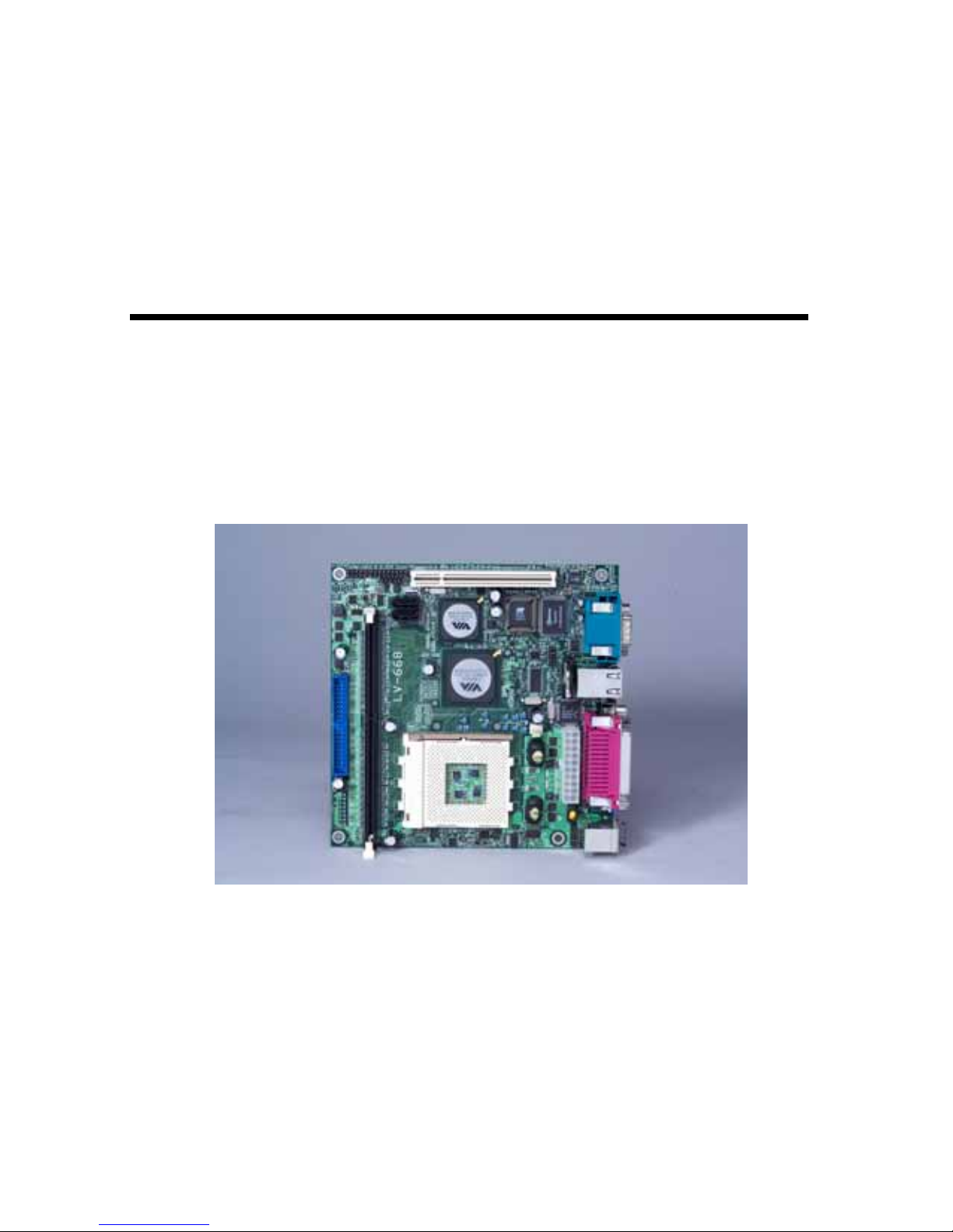
LV-668
Mini-ITX Motherboar d
User’s Manual
Edition 1.0
2005/09/30
Page 2

LV-668 User’s Manual
2
Copyright
Copyright 2004 - 2005. All rights reserved. This document is copyrighted and all rights are
reserved. The information in this document is subject to change without prior notice to make
improvements to the products.
This document contains proprietary informati on and protected by copyright. No part of this
document may be reproduced, copied, or translated in any f orm or a ny means without prior
written permission of the manufacturer.
All trademarks and/or registered trademarks contains in this docume nt are property of their
respective owners.
Disclaimer
The company shall not be liable for any incidenta l or cons equenti al dam ages resultin g from
the performance or use of this product.
The company does not issue a warrant y of any kind, express or implied, including without
limitation implied warranties of merchantability or fitness for a particular purpose.
The company has the right to revise the manual or inc lude changes in the specific ations of
the product described within it at any time without notice and without obligation to notify any
person of such revision or changes.
Trademark
All trademarks are the property of their respective holders.
Any questions please visit our website at http://www.commell.com.tw
Page 3
LV-668 User’s Manual
3
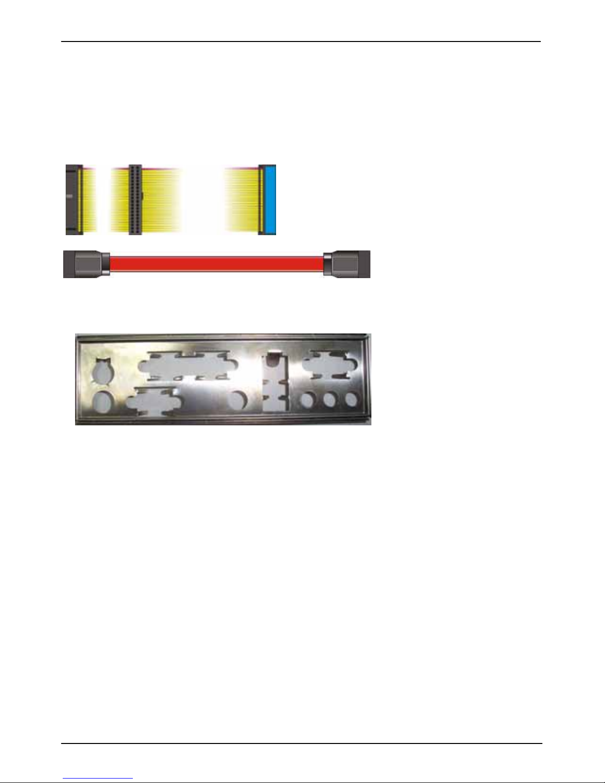
Packing List
Please check the package before you starting setup the system
Hardware:
LV-668 series motherboard x 1
Cable Kit:
40-pin ATA100 IDE flat cable x 1
Serial ATA ribbon cable x 1
I/O Shield x 1
Page 4

LV-668 User’s Manual
4
Index
Chapter 1 <Introduction>.....................................................................................7
1.1 <Product Overview>.................................................................................7
1.2 <Product Specification>...........................................................................8
1.3 <Mechanical Drawing>...........................................................................10
1.4 <Block Diagram>.................................................................................... 11
Chapter 2 <Hardware Setup>.............................................................................12
2.1 <Connector Location>............................................................................12
2.2 <Jumper Reference> .............................................................................13
2.3 <Connector Reference>.........................................................................14
2.3.1 <Internal Connector>..................................................................14
2.3.2 <External Connector>.................................................................14
2.4 <CPU and Memory Setup>....................................................................15
2.4.1< CPU>........................................................................................15
2.4.2 <Memory> ..................................................................................15
2.5 <CMOS Setup>......................................................................................16
2.6 <Enhanced IDE & CF Interface>............................................................17
2.7 <Serial ATA Interface>...........................................................................18
2.8 <LAN Interface>.....................................................................................19
2.9 <Onboard Display Interface>.................................................................20
2.9.1 <Analog VGA Interface> ............................................................20
2.10 <Onboard Audio Interface>..................................................................21
2.11 <Power and Fan Connector>...............................................................22
2.11.1 <Power Input>..........................................................................22
2.11.2 <Fan Connector>......................................................................22
2.12 <Indicator and Switch>.........................................................................23
Chapter 3 <System Configuration>...................................................................25
3.1 <SATA RAID Configuration>..................................................................25
Page 5

LV-668 User’s Manual
5
3.2 <Audio Configuration> ...........................................................................27
3.3 <Display Configuration>.........................................................................28
Chapter 4 <BIOS Setup> ....................................................................................30
Appendix A <I/O Port Pin Assignment> ...........................................................32
A.1 <IDE Port>.............................................................................................32
A.2 <IrDA Port>............................................................................................32
A.3 < VGA Port >..........................................................................................33
A.4 <Serial ATA Port>...................................................................................33
A.5 <Serial Port>..........................................................................................33
A.6 <LAN Port>............................................................................................34
A.7 <PS/2 Keyboard & Mouse Port>............................................................34
A.8 <CPU V oltage>…...................................................................................35
A.9<USB Interface>……………………………………………………………..35
Appendix B <Flash BIOS>..................................................................................37
B.1 BIOS Auto Flash T ool......................................................................37
B.2 Flash Method...................................................................................37
Appendix C <System Resources> ....................................................................39
C.1 <I/O Port Address Map>……………………………………………………39
C.2 <Memory Address Map>.......................................................................41
C.3 <System IRQ & DMA Resource>..........................................................42
C.3.1 <IRQ> ........................................................................................42
Contact Information............................................................................................44
Page 6

LV-668 User’s Manual
6
(The Page is Left For Blank)
Page 7

LV-668 User’s Manual Introduction
Product Overview
7
Chapter 1 <Introduction>
1.1 <Product Overview>
LV-668 is the Mini-ITX motherboard based on VIA chipset. It integrates the last VIA
embedded chipset for KN400A with VT8237R, DDR266/333/400 SDRAM, and serial ATA
with RAID to provide the economical embedded platform.
VIA KN400A & VT8237R Chipset
The board comes with the VIA last embedded chipset of KN400A, supports
DDR266/333/400 SDRAM, integrated the S3 Graphics UniChrome Pro IGP graphics core,
hardware MPEG-2 and MPEG-4 acceleration.
The VT8237R provides the board to supp ort Ultra V-Link (1GB/s) with KN400A, two serial
ATA ports with RAID array function, 4 x USB2.0 ports and 5.1 channel AC97 audio.
Multimedia solution
Based on VIA KN400A chipset, the board provides, which supports single independent
display with CRT.
LAN Interface
LV-668 also comes with one 10/100Mbps LAN interface, support boot-on-LAN and
wake-on-LAN function.
High Speed Hot-plug Interface
Based on VIA VT8237R, the board provides 4 USB2.0 interfaces with up to 480Mbps of
transferring rate.
Expanded UCR for remote Operating SETUP Bios Feature
Expanded Universal Console Redirection (UCR) is a feature for monitoring POST
messages and running Setup and an operation s ystem from a remote ser ial terminal.
Page 8

LV-668 User’s Manual Introduction
Product Specification
8
1.2 <Product Specification>
General Specification
Form Factor Mini-ITX motherboard
CPU
AMD Geode NX Processors
NX 1250@6W/1500@6W Processors supported
Fanless with CPU heatsink
Memory 1 x 184-pin DDR 266/333/400 SDRAM up to 1GB
Unbufferred, none-ECC memory supported only
Chipset VIA KN400A and VT8237R
BIOS Phoenix-Award v6.00PG 4Mb PnP flash BIOS
Green Function Power saving mode includes doze, standby and suspe nd modes.
ACPI version 1.0 and APM version 1.2 compliant
Real Time Clock VIA VT8237R built-in RTC with lithium battery
Enhanced IDE Enhanced IDE interface supports dual channels and up to 2
ATAPI devices at Ultra DMA100
One 40-pin onboard
Serial ATA VIA VT8237R integrates 2 Serial ATA interface
RAID 0, 1 array Technology supported
Multi-I/O Port
Chipset VIA VT8237R with Winbond W83697HF controller
Serial Port one external RS-232 serial port on rear I/O panel.
USB Port Four Hi-Speed USB 2.0 ports with 480Mbps of transfer rate.
Parallel Port One external parallel port on rear I/O panel.
IrDA Port One IrDA compliant Infrared interface supports SIR.
K/B & Mouse External PS/2 keyboard and mouse ports on rear I/O panel
Hardware
Monitor
Fan speed, CPU temperature and voltage monitoring
VGA Display Interface
Chipset VIA KN400A built-in S3 Graphics UniChrome Pro IGP graphics
core
Core Frequency 200MHz
Memory BIOS selectable 16/32/64MB shard with system memory
Display Type CRT, LCD monitor with analog display
Connector External DB15 female connector on rear I/O panel
Page 9

LV-668 User’s Manual Introduction
Product Specification
9
Ethernet Interface
Chipset AMD AM79C874VI
Type 10Base-T / 100Base-TX
auto-switching Fast Ethernet
Full duplex, IEEE802.3U compliant
Connector One External RJ45 connectors with LED on rear I/O panel
Audio Interface
Chipset Realtek® ALC655 AC97 3D audio codec
Interface 5.1 channel 3D audio with Line-in, Line-out and MIC-in
Connector External Audio phone jack for Line-out/Front, Line-in/Rear and
MIC(stereo)-in/Center
Onboard audio connector with pin header
Onboard CD-IN connector
Expansive Interface
PCI 1 x PCI slot supports up to one PCI devices through riser card
Power and Environment
Power
Requirement
Standard ATX 20-pin power supply
Dimension 170 (L) x 170 (H) mm
Temperature Operating within 0 ~ 60oC (32 ~ 140oF)
Storage within -20 ~ 85
o
C (-4 ~ 185oF)
Software support
Operation
System
Windows 2000, Windows XP
Linux (Fedora Core 1, Mandrake 9.2 and Red Hat 9.0)
Ordering Code
LV-668 AMD Geode NX processors Mini-ITX motherboard with onboard
VGA, LAN, SATA, USB 2.0 Ports, Audio, 1 x RS232 serial port,
S/PDIF,Parallel port
LV-668-12 Same as LV-668 and with AMD Geode NX 1250 processor
Lv-668-15 Same as LV-668 and with AMD Geode NX 1500 processor
1. Please do not order other Mini-AGP modules excluded in the list for this board.
2. The specifications may be different as the actual production.
For further product information please visit the website at
http://www.commell.com.tw
Page 10
LV-668 User’s Manual Introduction
Product Specification
10
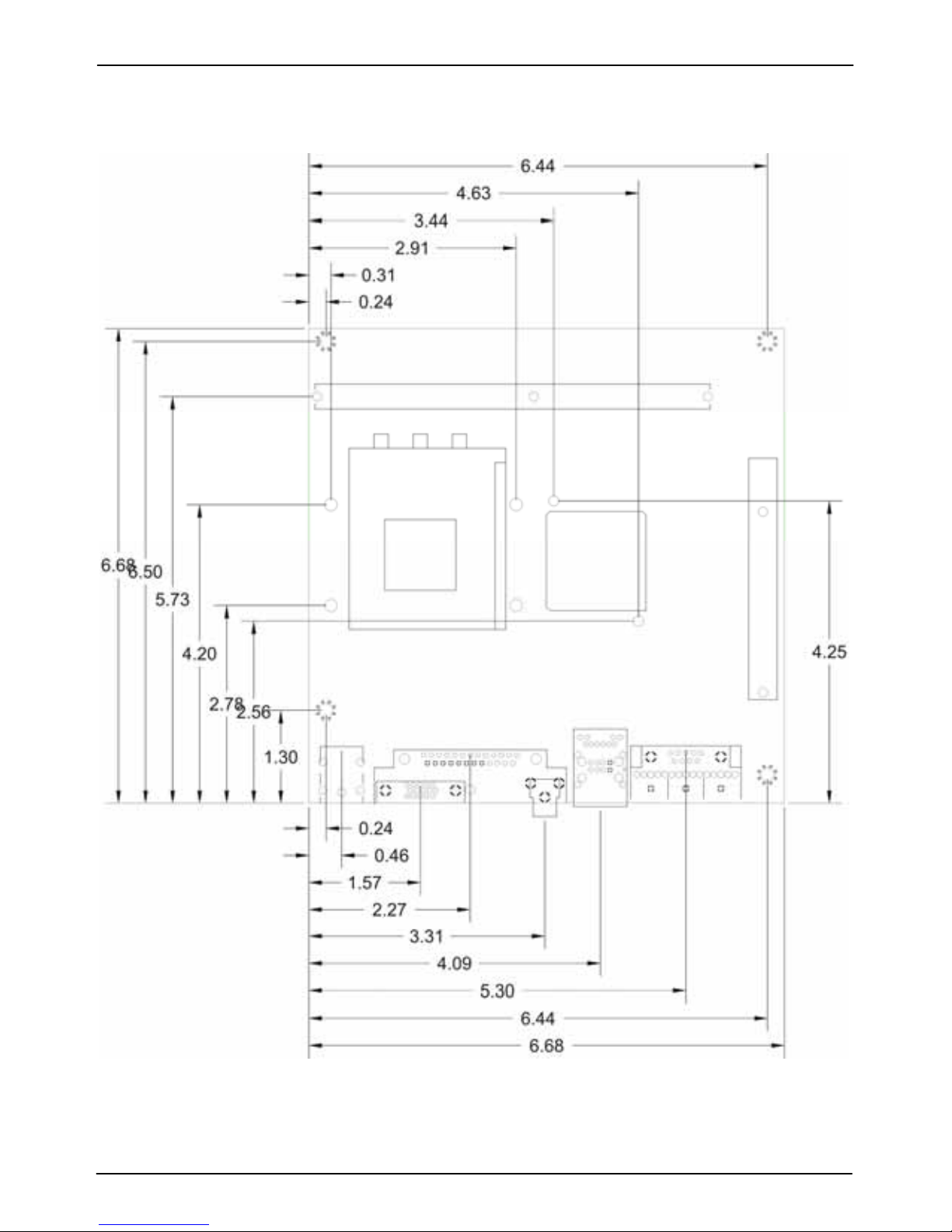
1.3 <Mechanical Drawing>
Page 11
LV-668 User’s Manual Introduction
Product Specification
11
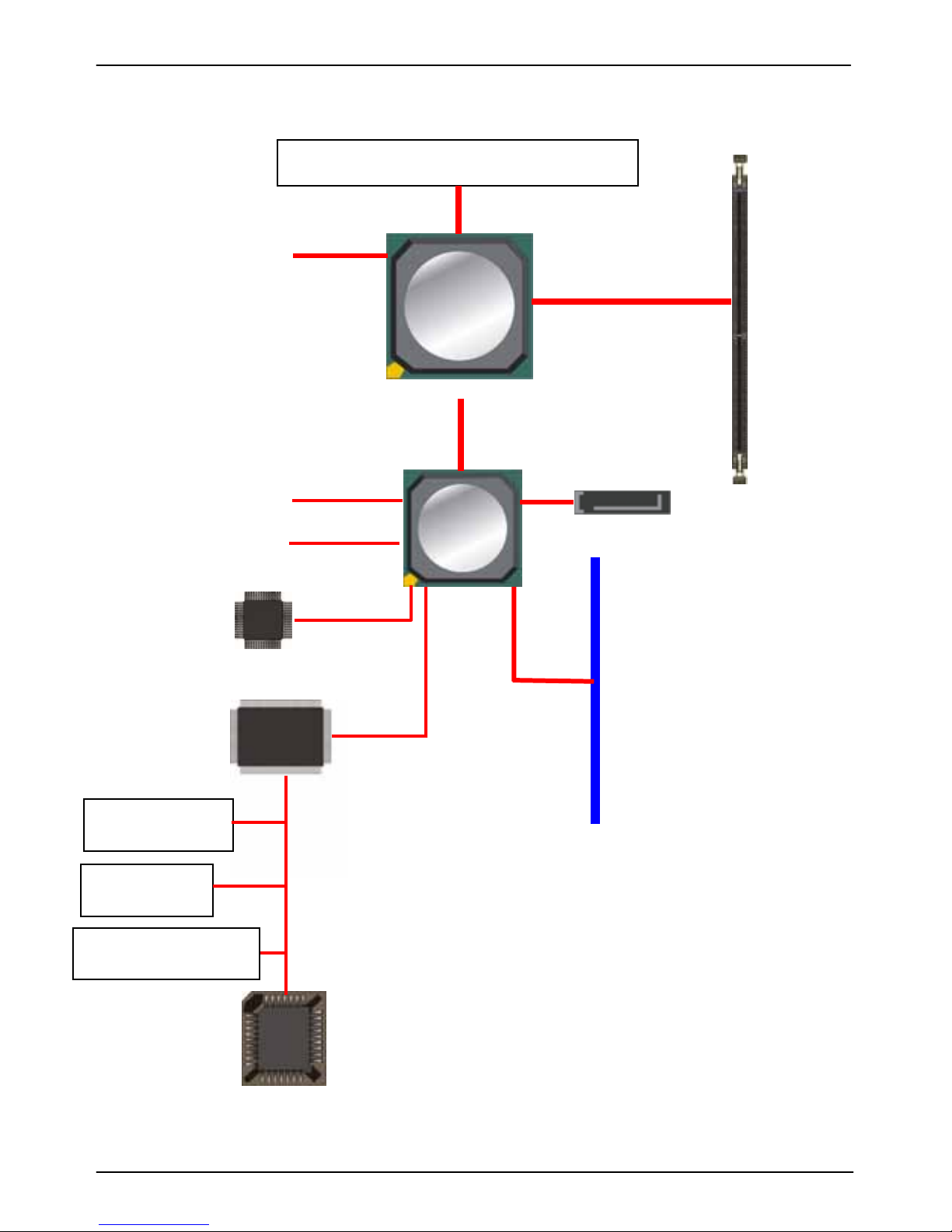
1.4 <Block Diagram>
A
MD Geode NX processo
r
1 x 184-pin
DDR266/333/400
U
p
to 1GB
CRT/LCD Monitor
KN400A
Ultra V-Link
1GB/s
VT8237R
4 x USB2.0 Ports
IDE
1 x Serial ports
1 x Parallel ports
IrDA
AC97 5.1CH Codec
PCI
2 x SATA
BIOS
Page 12
LV-668 User’s Manual Hardware Setup
Jumper Reference
12
Chapter 2 <Hardware Setup>
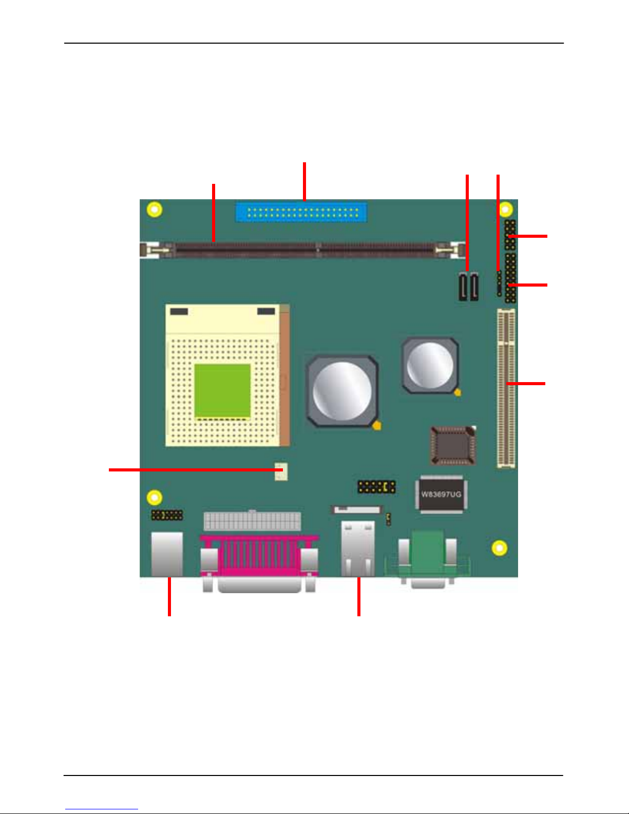
2.1 <Connector Location>
J2
J6
J3
J7
J4/J5
DIMM
J11
J10
J19
J3&17
J21
J16
Page 13
LV-668 User’s Manual Introduction
Product Specification
13
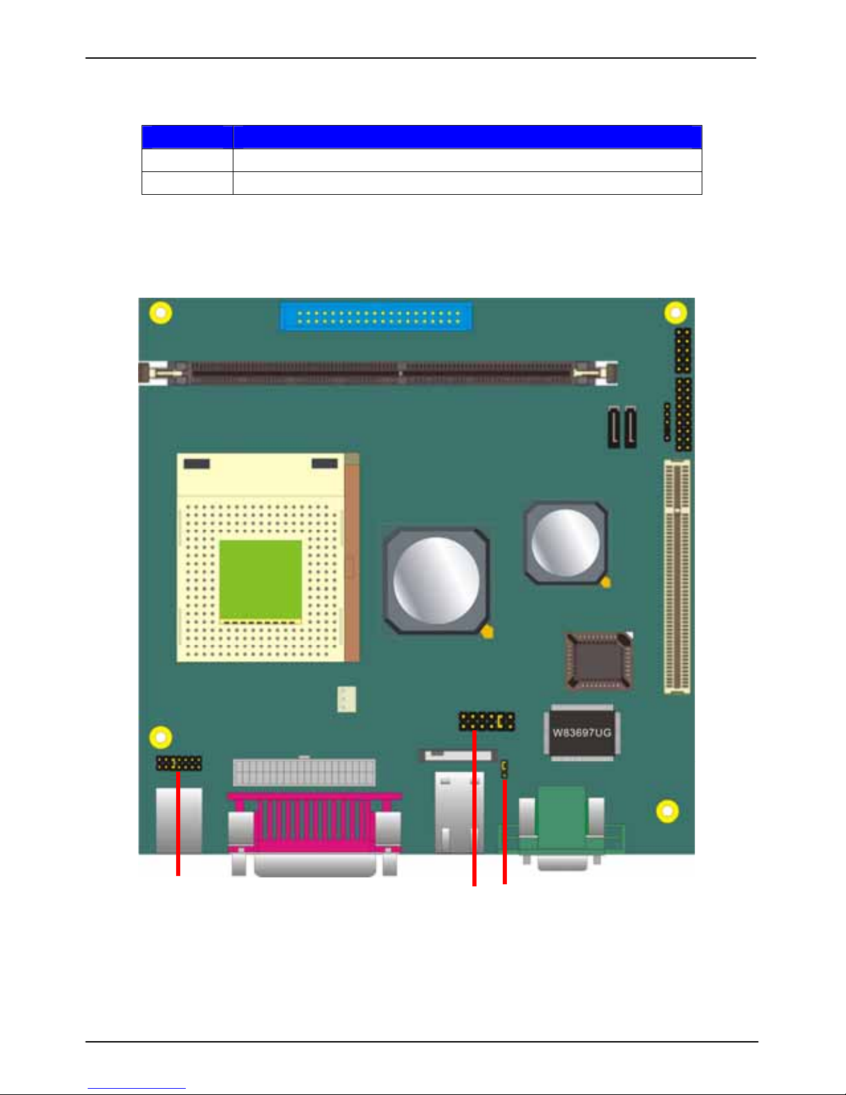
2.2 <Jumper Reference>
Jumper Function
J13 CMOS Operating/Clear Setting.
J14 Setting CPU voltage.
J12 J13 J14
Page 14
LV-668 User’s Manual Hardware Setup
Jumper Reference
14
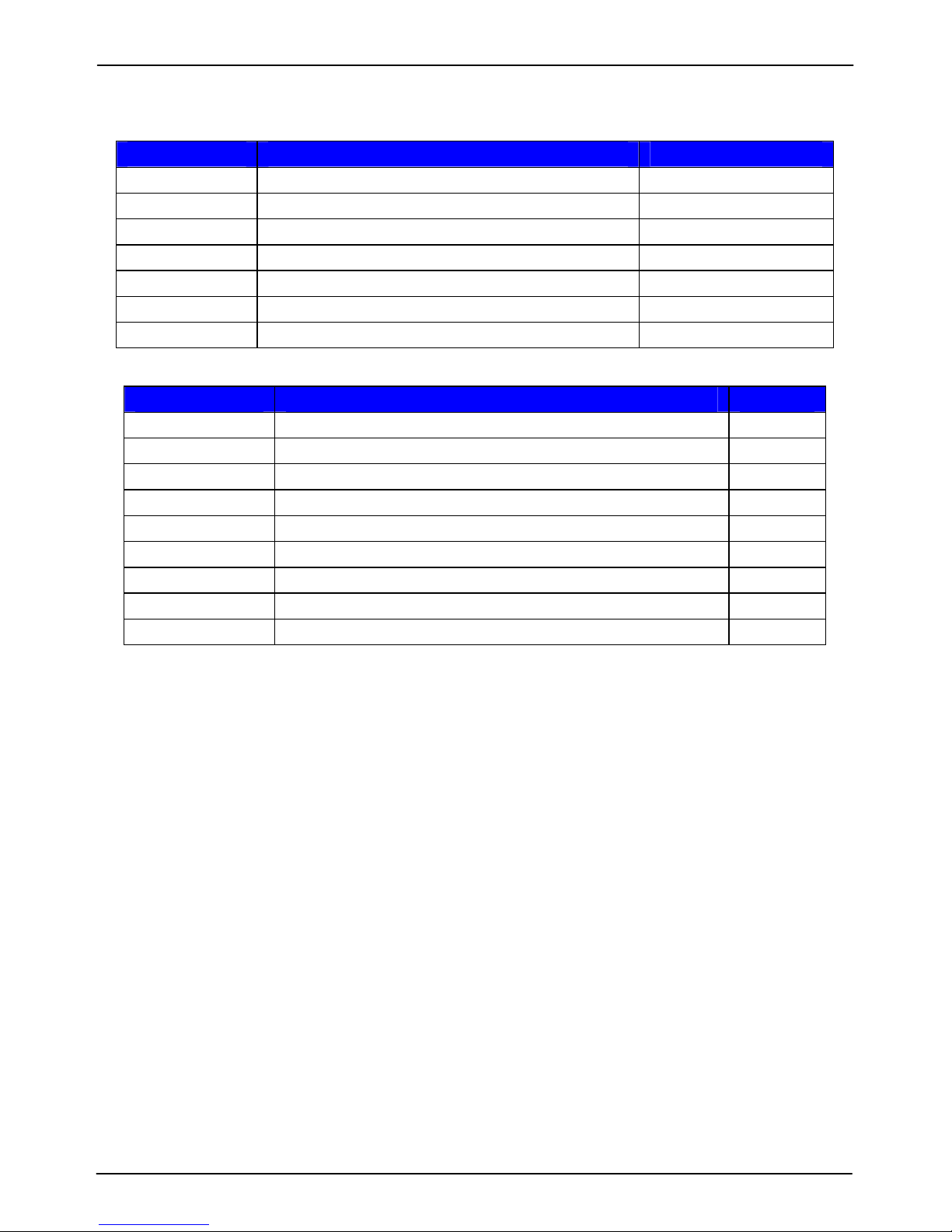
2.3 <Connector Reference>
2.3.1 <Internal Connector>
Connector Function Remark
DIMM 184-pin DDR SDRAM DIMM Standard
J2 40-pin primary IDE connector Standard
J4/J5 7-pin Serial ATA connector Standard
J15 20-pin power supply connector Standard
J3 5 x 2-pin USB connector Standard
J10 3-pin CPU cooler fan connector Standard
J7 14-pin switch/indicator connector Standard
2.3.2 <External Connector>
Connector Function Remark
J18 DB15 VGA connector Standard
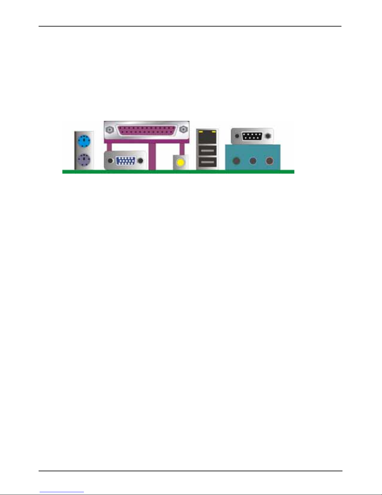
J3/J17 Dual USB and RJ45 LAN connector Standard
J21 Serial port connector Standard
J19 PS/2 Keyboard/Mouse connector Standard
J20 S/PDIF Digital Audio out RCA
J21(Green) Audio Line-out port Standard
J21(Blue) Audio Line-in port Standard
J21(Pink) Audio Microphone input port Standard
J16 One parallel port Standard
Page 15
LV-668 User’s Manual Introduction
Connector Reference
15
2.4 <CPU and Memory Setup>
2.4.1< CPU>
The board supports AMD Geode NX 1250/1500 processor, with CPU headsink onl y .
2.4.2 <Memory>
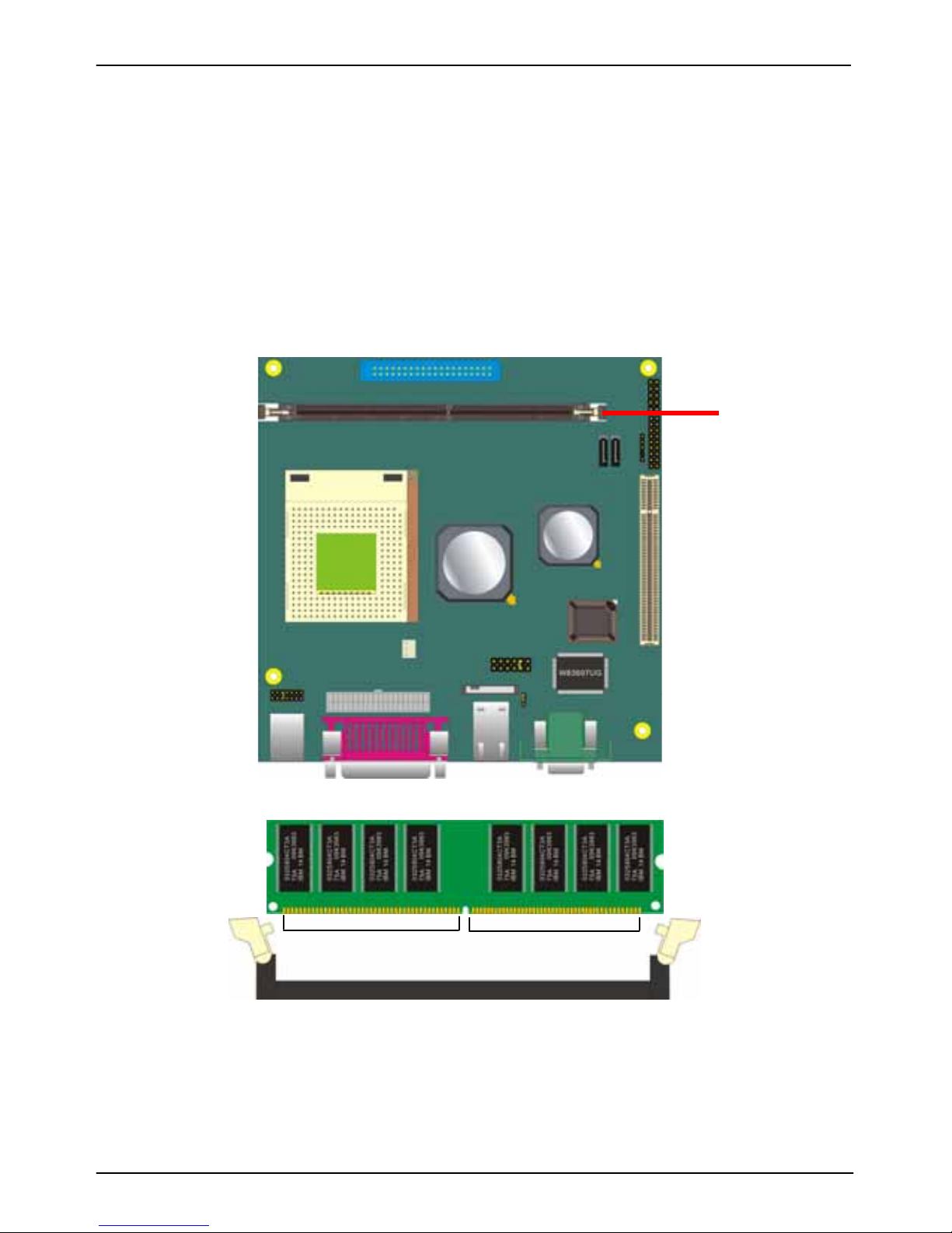
The board supports one 184-pin DDR266/333/400 SDRAM and up to 1GB of capacity, onl y
non-ECC, unbuffered memory is supported.
DIMM
104-pin 80-pin
Please check the pin number to match the socket side well
before installing memory module.
Page 16
LV-668 User’s Manual Hardware Setup
CPU and Memory Setup
16
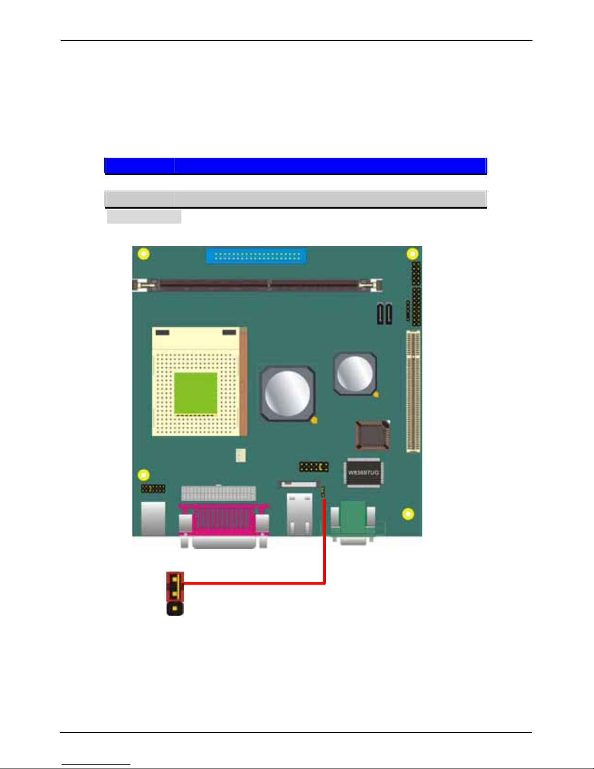
2.5 <CMOS Setup>
The board’s data of CMOS can be setting in BIOS. If the board refuses to boot due to
inappropriate CMOS settings, here is how to proceed to clear (reset) the CMOS to its
default values.
Jumper: J13
Type: Onboard 3-pin jumper
J13 Mode
1-2 Normal Operation
2-3 Clear CMOS
Default setting
1
3
J13
Page 17
LV-668 User’s Manual Introduction
CMOS Setup
17
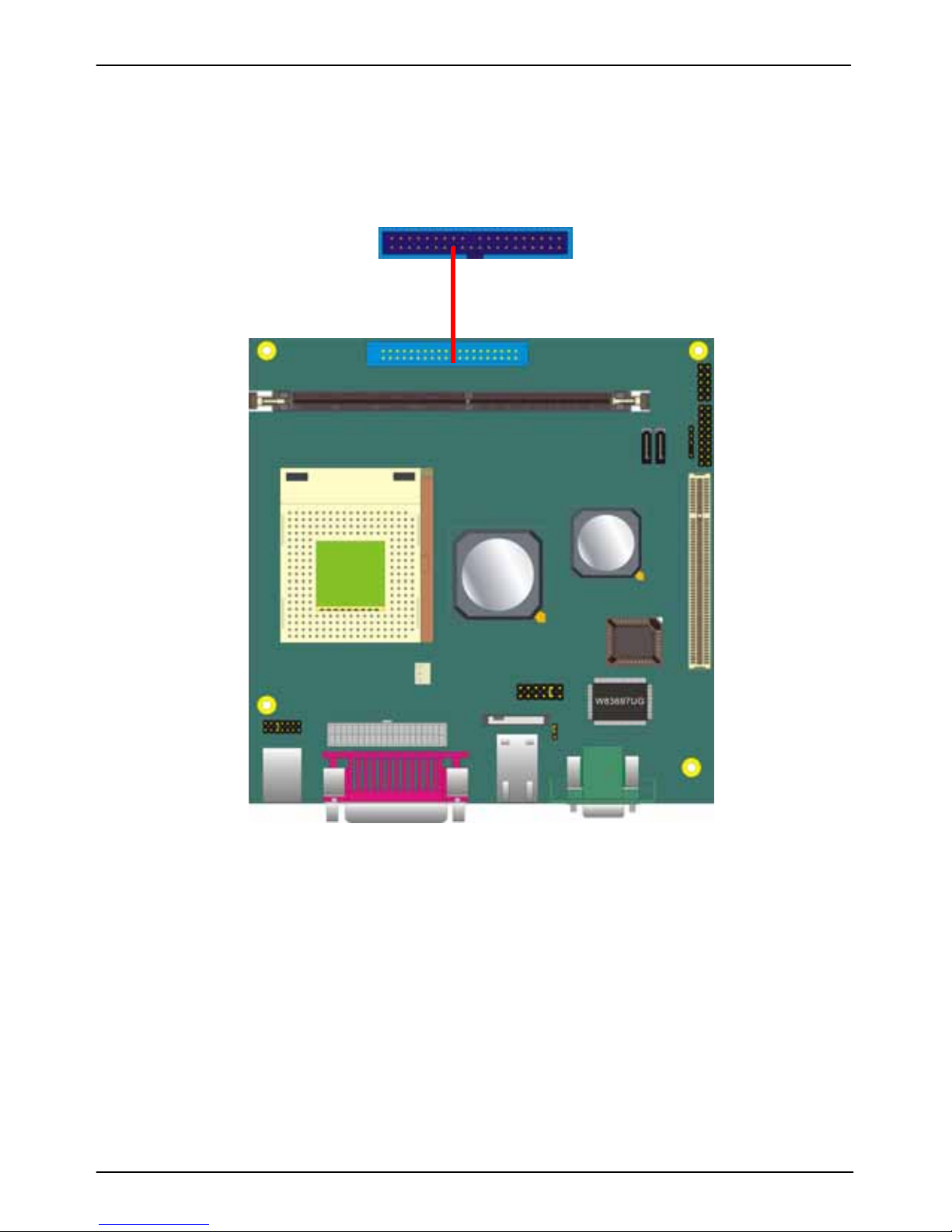
2.6 <Enhanced IDE & CF Interface>
The board supports one enhanced IDE interface, one channel for 2 ATAPI devices with
ATA100.
J2
Page 18
LV-668 User’s Manual Hardware Setup
Enhanced IDE & CF Interface
18
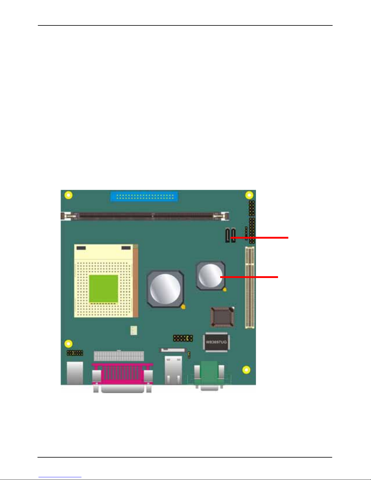
2.7 <Serial ATA Interface>
Based on VIA VT8237R Southbridge, the board supports two Serial ATA interfaces with
RAID 0 and 1 array function. The following is the list of the specification of the Serial ATA.
1. Complies with Serial ATA Specification Revision 1.0
2. Dual Channel master mode PCI
3. On-chip two-channel Serial ATA (S-ATA) for support of up to two S-ATA devices
directly.
4. S-ATA drive transfer rate is capable of up to 150 MB/s per channel (serial spee d of 1.5
Gbit/s).
For more information please visit VIA website (www.via.com.tw)
J4/J5
VT8237R
Page 19
LV-668 User’s Manual Introduction
Serial ATA Interface
19
2.9 <LAN Interface>
The board provides one 10/100Mbps LAN interfaces with AM79C874VI , and compliant with
standard IEEE 802.3 Ethernet interface for 100BASE-TX.
J17
Page 20
LV-668 User’s Manual Hardware Setup
Onboard Audio Interface
20
2.10 <Onboard Display Interface>
Based on VIA KN400A, the board supports integrated S3 Graphics UniChrome Pro IGP
graphics, with BIOS selectable 16/32/64MB shared with system memory for frame buffer.
2.10.1 <Analog VGA Interface>
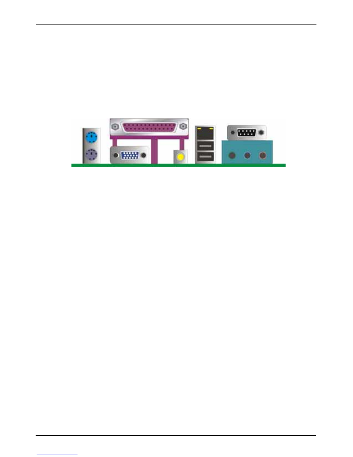
The board provides a DB15 VGA connector on the rear I/O panel .
J18
Page 21
LV-668 User’s Manual Introduction
Serial ATA Interface
21
2.11 <Onboard Audio Interface>
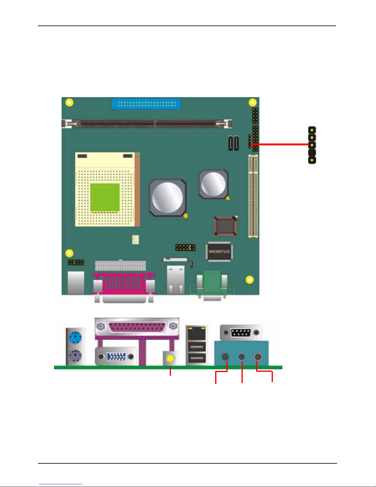
The board provides the onboard Realtek ALC 655 AC97 5. 1-channel audio interface , with
three phone jacks on rear I/O panel for Line-out, Line-in, MIC(stereo)-in as 2-channel sound
system, and Front, Rear, Center as 5.1-channel sound system.
1
4
J6
J20
Line-out Line-in MIC-in (system setup with 2-channel)
Page 22
LV-668 User’s Manual Hardware Setup
Power and Fan Connector
22
2.15 <Power and Fan Connector>
2.15.1 <Power Input>
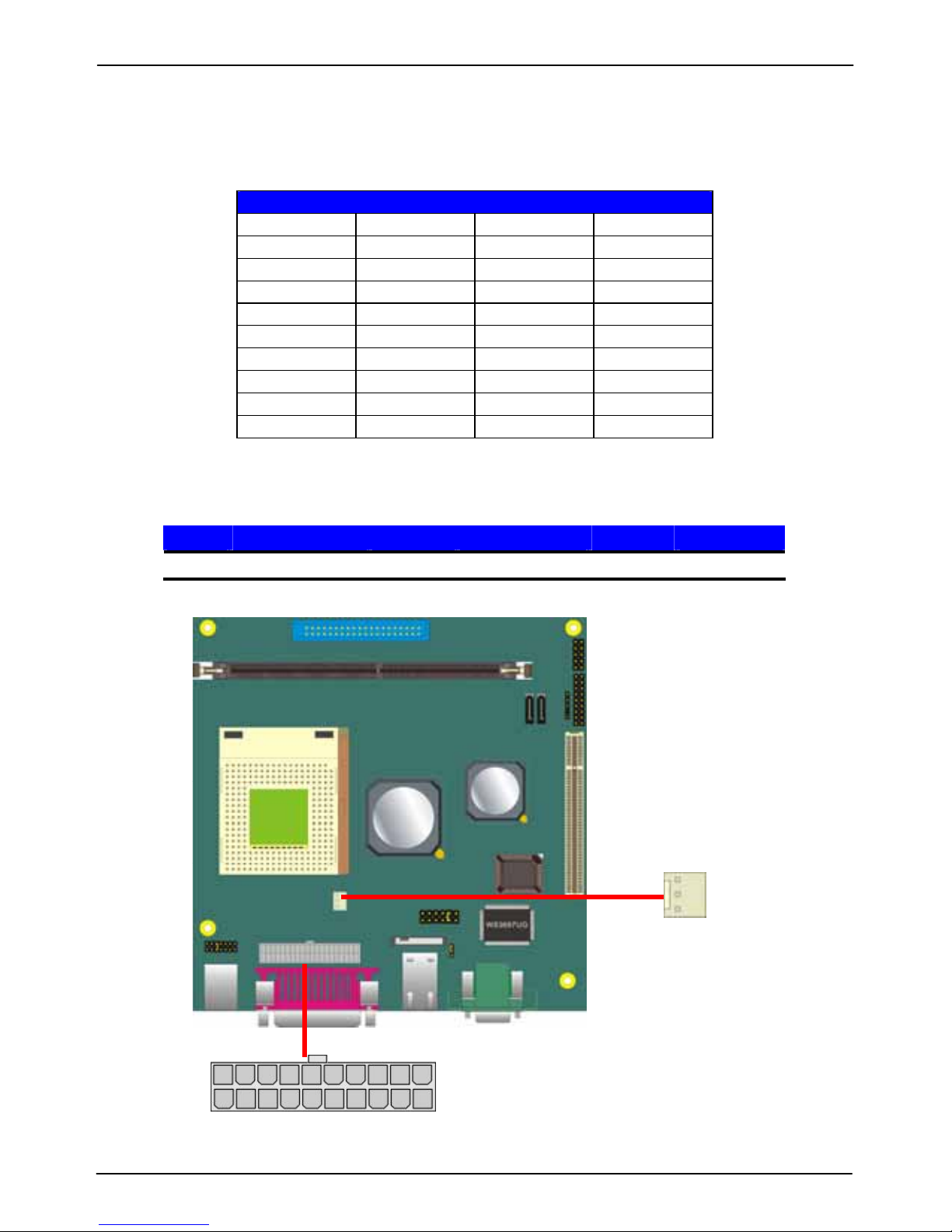
Connector: J15
Type: 20-pin ATX power connector
PIN assignment
1 12V 11 5V
2 5VSB 12 5V
3 PWOK 13 -5V
4 GND 14 GND
5 5V 15 GND
6 GND 16 GND
7 5V 17 PSON
8 GND 18 GND
9 3.3V 19 -12
10 3.3V 20 3.3V
2.15.2 <Fan Connector>
Connector: J10
Type: 3-pin fan wafer connector
Pin Description Pin Description Pin Description
1 Ground 2 +12V 3 Fan Sensor
3
1
J10
J15
Page 23
LV-668 User’s Manual Introduction
Indicator and Switch
23
2.16 <Indicator and Switch>
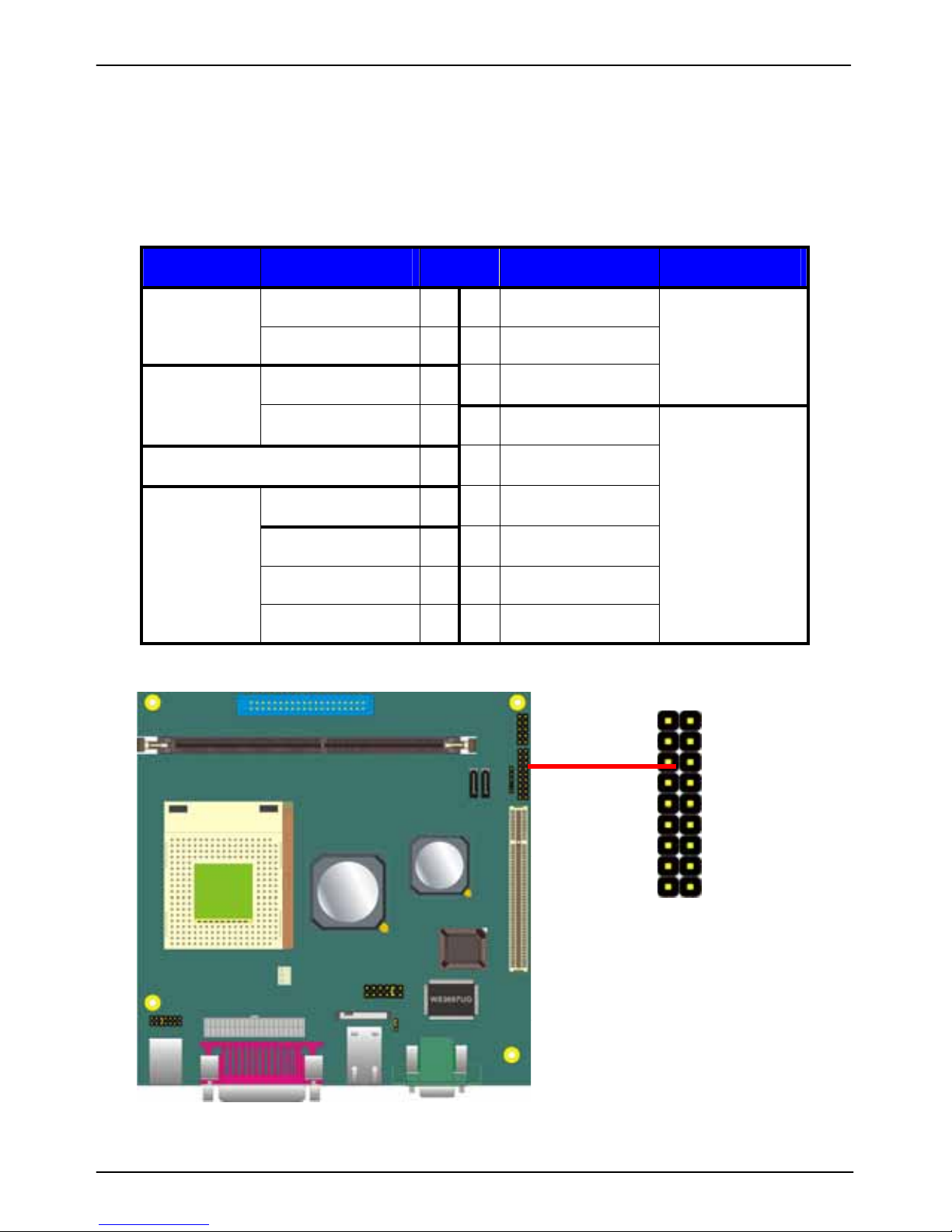
The J7 provides front control panel of the board, such as power button, reset and beeper,
etc. Please check well before you connecting the cables on the chassis.
Function Signal PIN Signal Function
VCC 1 2 HD_H +
PWR_LED+ 3 4 HD_L -
PWR_LED- 5 6 PWR_SW+
SPK+ 7 8 PWR_SW -
N/C 9 10 RST_SW +
N/C 11 12 RST_SW -
SPK- 13 14 SLPLED +
SLPBTN_L+ 15 16 SLPLED -
SLPBTN_L- 17 18 N/C
1 2
17 18
J7
Page 24

LV-668 User’s Manual
24
(This Page is Left For Blank)
Page 25
LV-668 User’s Manual System Configuration
SATA RAID Configuration
25
Chapter 3 <System Configuration>
3.1 <SATA RAID Configuration>
The board supports two Serial ATA ports onboard, and supports RAID 0, 1 and disk arra y,
the RAID 0, 1 and specified below:
RAID 0 (Stripping): Two hard drives operating as one drive for optimized data R/W
performance. It needs two unused drives to build this operation.
RAID 1 (Mirroring): Copies the data from first drive to second drive for data security, and if
one drive fails, the system would access the applications to the workable drive. It needs two
unused drives or one used and one un used drive to build t his operation. The second dr ive
must be the same or lager size than first one.
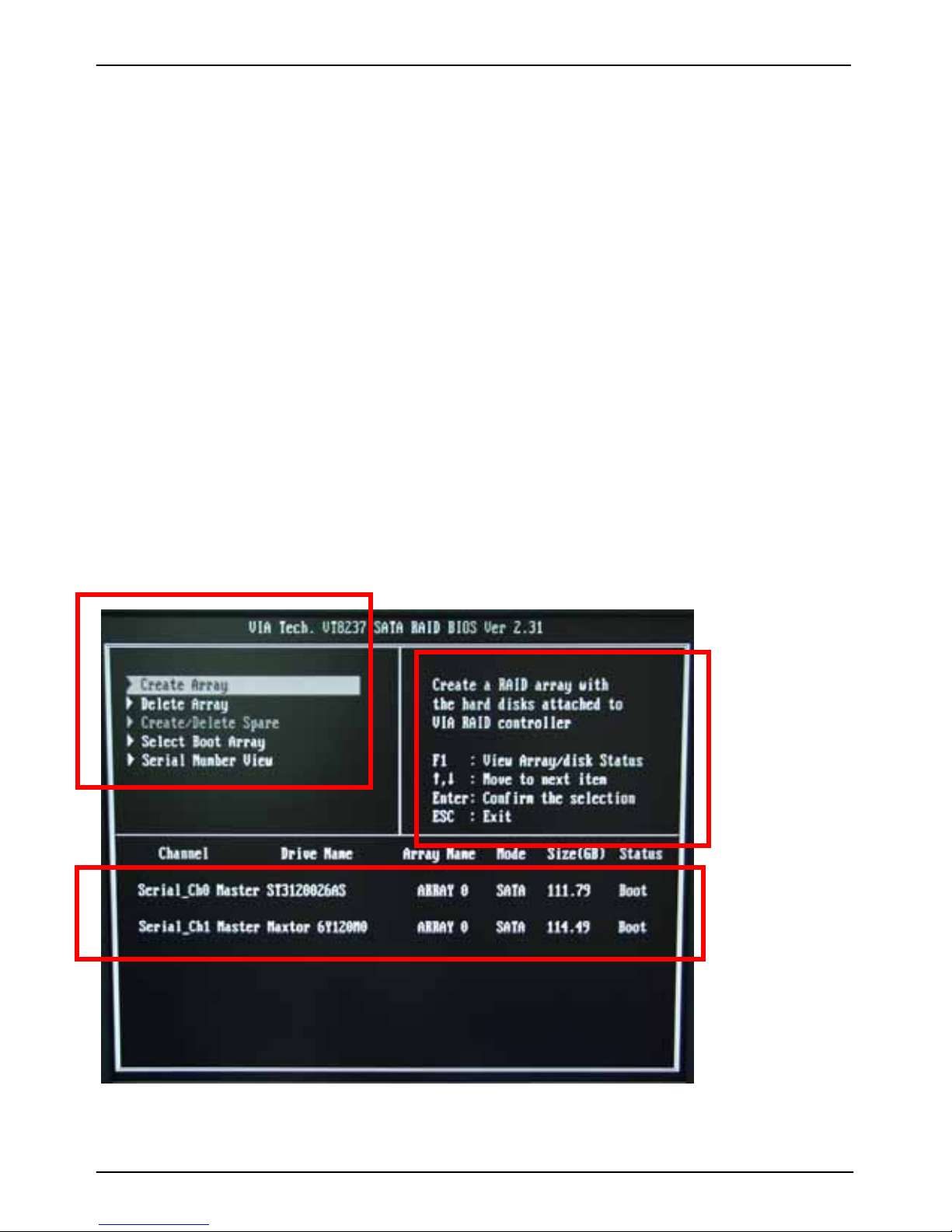
To build Serial ATA disk array, please press <TAB> while booting up the system before
entering OS, and follow the instructions to edit the RAID function.
(Selectable Functions)
(Option Instruction)
(Disk Statement)
Page 26
LV-668 User’s Manual System Configuration
SATA RAID Configuration
26
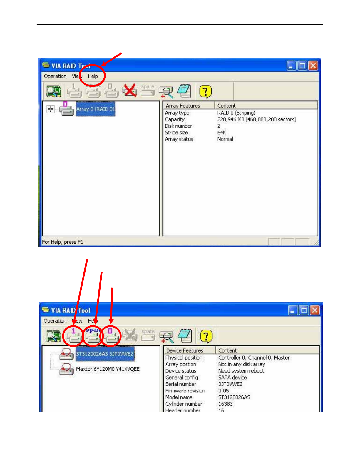
You also can edit disk array under OS, please install the VIA RAID Utility in the driver CD.
(To getting start, please click here to learn more information)
(Click here to build RAID 0)
(Click here to build RAID 0)
(Click here to build RAID JBOD)
Page 27
LV-668 User’s Manual System Configuration
Audio Configuration
27
3.2 <Audio Configuration>
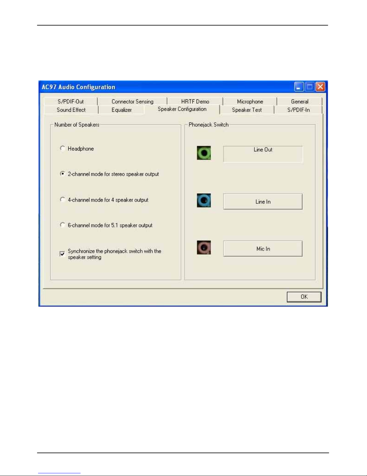
The board provides 5.1 channel audio interface with driver installe d, please install the VIA
audio driver in the CD before getting start to enjoy the 5.1 channel sound system.
Page 28
LV-668 User’s Manual System Configuration
Display Configuration
28
3.3 <Display Configuration>
The board provides onboard anal og VGA i nterface, and , ple ase install t he VIA video driv er
before enjoy the vivid display.
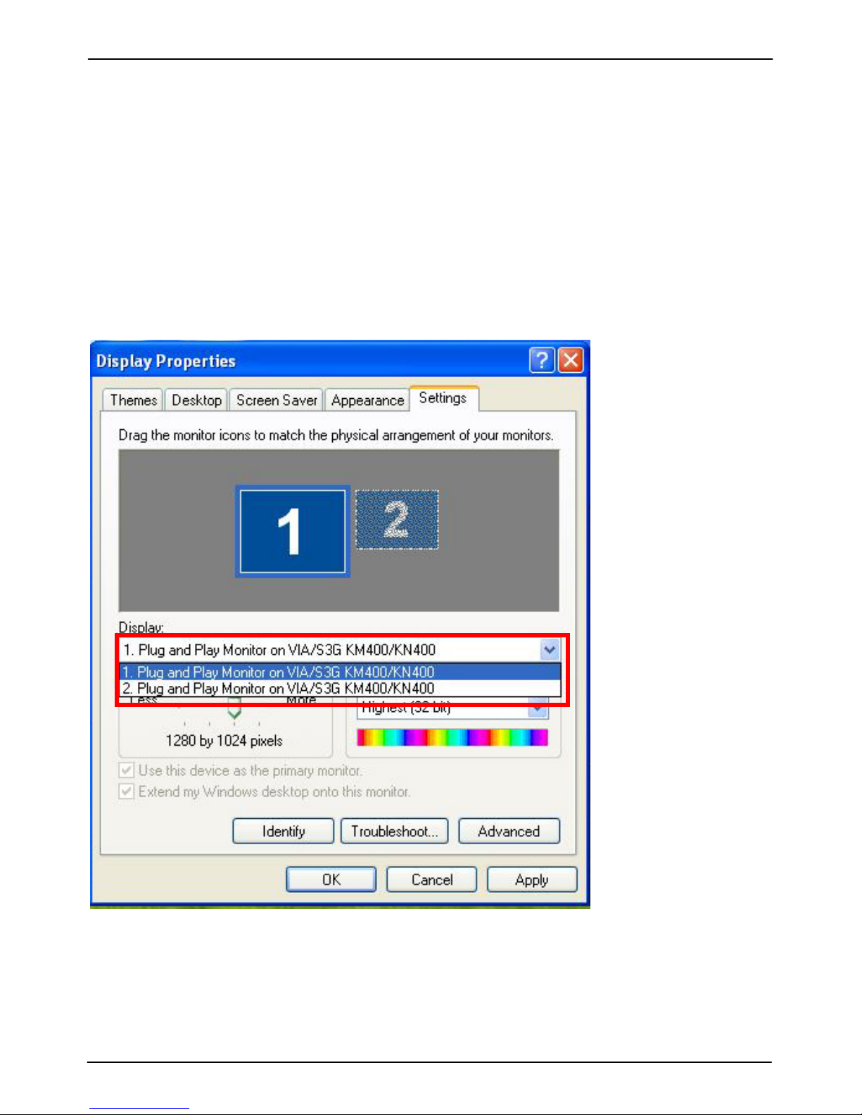
Based on the VIA KN400A with S3 UniChrome Pro graphic, the board provides dual display
function for clone or extended desktop modes with secondary display device attached.
After installing video driver, please launch the desktop display properties.
For secondary display device, you have two options selectable.
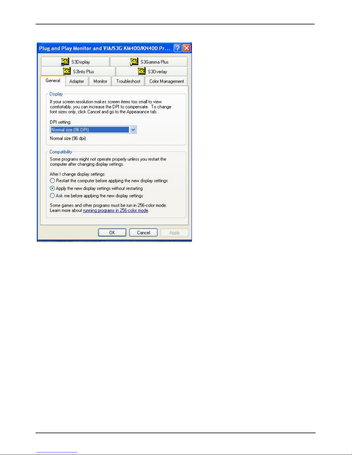
For more display properties setting, please click “Advanced” button.
Page 29
LV-668 User’s Manual System Configuration
Display Configuration
29
Please select S3Display for advanced device setting.
Page 30
LV-668 User’s Manual
30
Chapter 4 <BIOS Setup>
The motherboard uses the Award BIOS for the system configuration. The Award
BIOS in the single board computer is a customized version of the industrial standard
BIOS for IBM PC AT-compatible computers. It supports Intel x86 and compatible CPU
architecture based processors and computers. The BIOS provides critical low-level
support for the system central processing, memory and I/O sub-systems.
The BIOS setup program of the single board computer let the customers modify the
basic configuration setting. The settings are stored in a dedicated battery-backed
memory, NVRAM, retains the information when the power is turned off. If the battery
runs out of the power, then the settings of BIOS will come back to the default setting.
The BIOS section of the manual is subject to change without notice and is provided here
for reference purpose only. The settings and configurations of the BIOS are current at
the time of print, and therefore they may not be exactly the same as that displayed on
your screen.
To activate CMOS Setup program, press <DEL> key immediately after you turn on
the system. The following message “Press DEL to enter SETUP” should appear in the
lower left hand corner of your screen. When you enter the CMOS Setup Utilit y, the Main
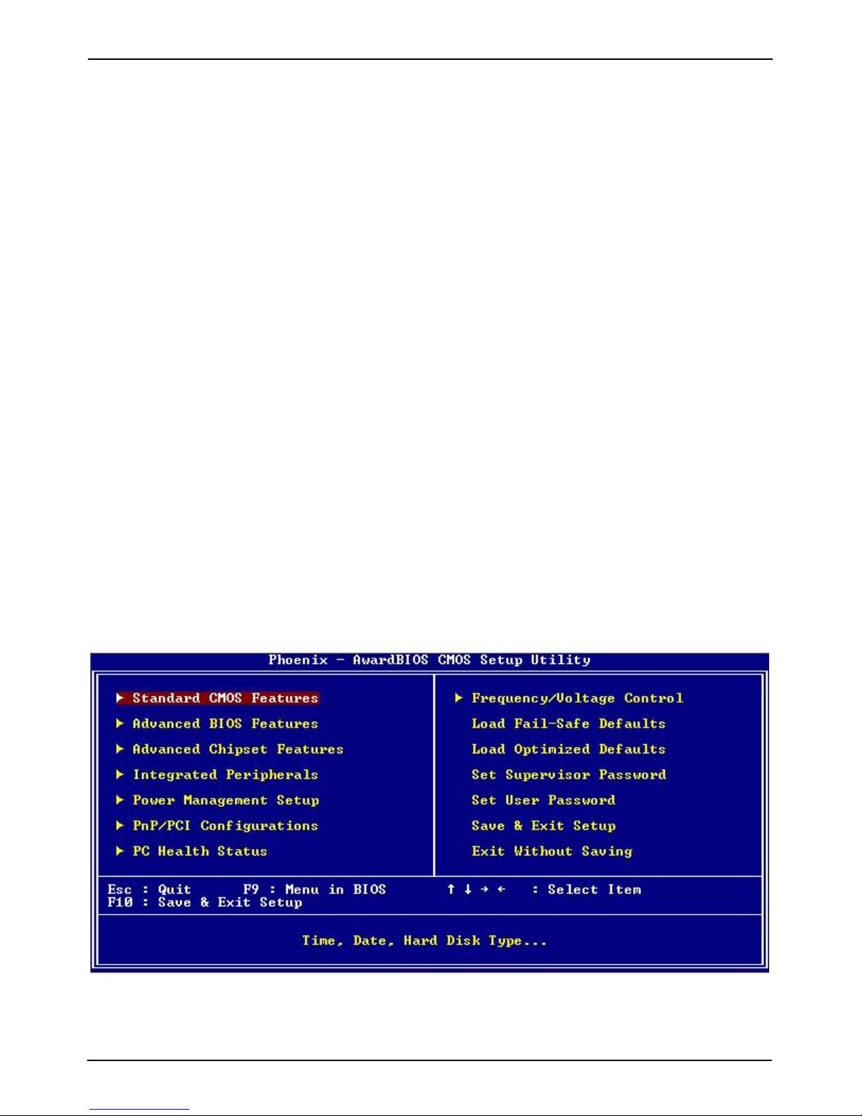
Menu will be displayed as Figure 4-1. You can use arrow keys to select your function,
press <Enter> key to accept the selection and enter the sub-menu.
Figure 4-1 CMOS Setup Utility Main Screen
Page 31

LV-668 User’s Manual BIOS Setup
Display Configuration
31
(This Page is Left for Blank)
Page 32
LV-668 User’s Manual
32
Appendix A <I/O Port Pin Assignment>
39
1
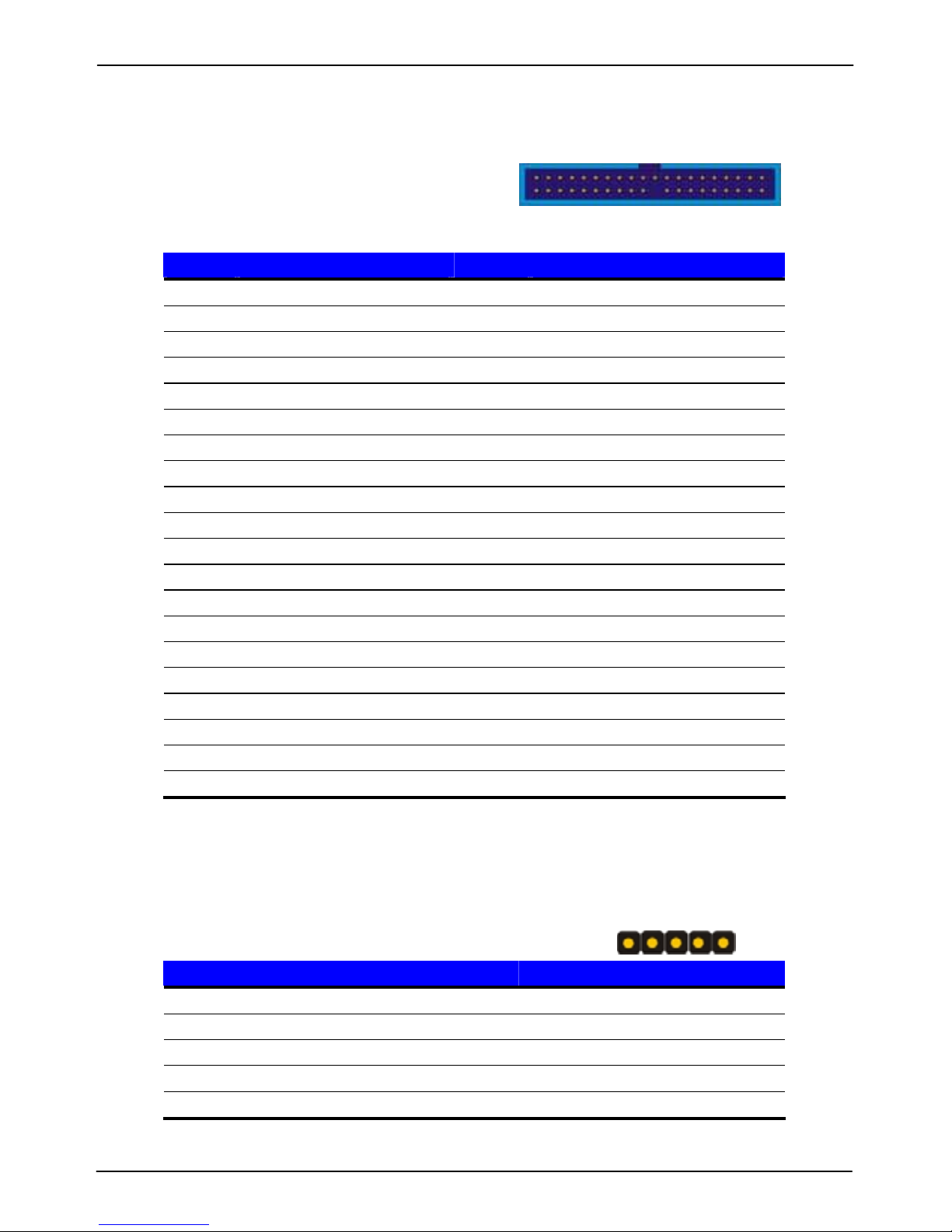
A.1 <IDE Port>
Connector: J2
Type: 40-pin (20 x 2) box header
40
2
Pin Description Pin Description
1 Reset 2 Ground
3 D7 4 D8
5 D6 6 D9
7 D5 8 D10
9 D4 10 D11
11 D3 12 D12
13 D2 14 D13
15 D1 16 D14
17 D0 18 D15
19 Ground 20 VCC
21 REQ 22 Ground
23 IOW-/STOP 24 Ground
25 IOR-/HDMARDY 26 Ground
27 IORDY/DDMARDY 28 DMA66#/DMA33
29 DACK- 30 Ground
31 IRQ 32 N/C
33 A1 34 CBLID
35 A0 36 A2
37 CS0 (MASTER CS) 38 CS1 (SLAVE CS)
39 LED ACT- 40 Ground
A.2 <IrDA Port>
5 1
Connector: J6
Type: 5-pin header for SIR Ports
Pin Description
1 Vcc
2 N/C
3 IRRX
4 Ground
5 IRTX
Page 33
LV-668 User’s Manual BIOS Setup
Floppy Port
33
6
10
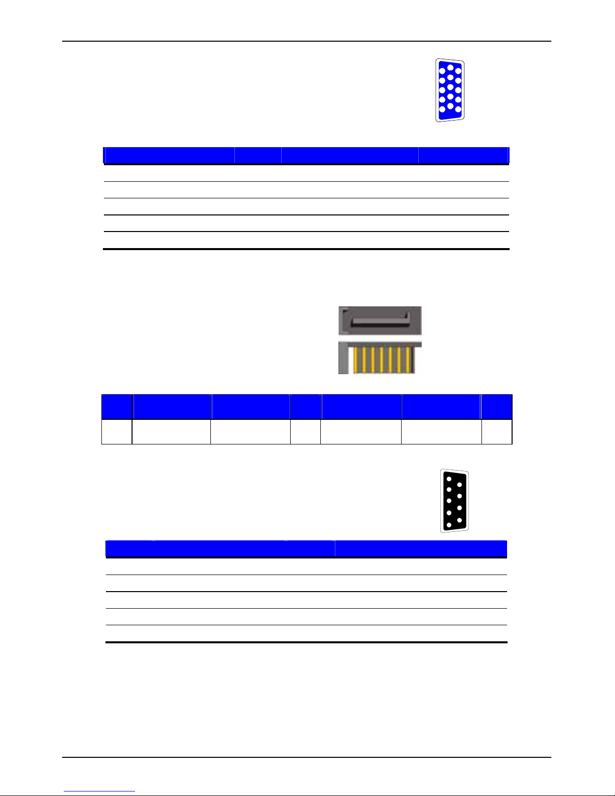
A.3 < VGA Port >
11
12
13
14
15
1
2
3
4
5
Connector: J18
Type: 15-pin D-sub female connector on bracket
Pin Description Pin Description Pin Description
1 RED 6 Ground 11 N/C
2 GREEN 7 Ground 12 5VCDA
3 BLUE 8 Ground 13 HSYNC
4 N/C 9 LVGA5V 14 VSYNC
5 Ground 10 Ground 15 5VCLK
A.4 <Serial ATA Port>
1 7
Connector:J4/J5
Type: 7-pin wafer connector
1 2 3 4 5 6 7
GND RSATA_TXP1 RSATA_TXN1 GND RSATA_RXN1 RSATA_RXP1 GND
A.5 <Serial Port>
1
2
3
4
5
6
7
8
9
Connector: COM1
Type: 9-pin D-sub male connector on bracket
Pin Description Pin Description
1 DCD 6 DSR
2 SIN 7 RTS
3 SO 8 CTS
4 DTR 9 RI
5 Ground
Page 34
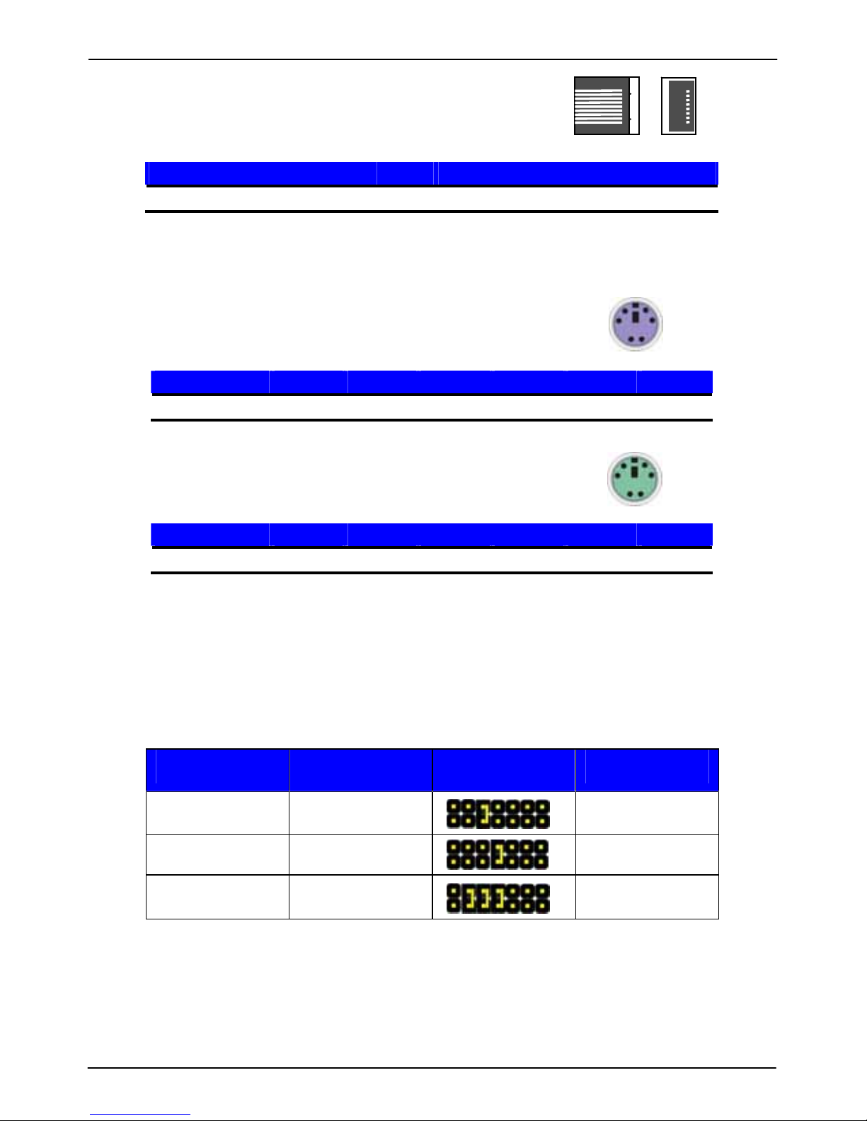
LV-668 User’s Manual
VGA Port
34
A.6 <LAN Port>
1
8
Connector: J17
Type: RJ45 connector with LED on bracket
Pin 1 2 3 4 5 6 7 8
Description TX+ TX- RX+ N/C N/C RX- N/C N/C
A.7 <PS/2 Keyboard & Mouse Port>
1 2
Connector: J19 (keyboard)
3 4
Type: 6-pin Mini-DIN connector on bracket
5 6
Pin 1 2 3 4 5 6
Description N/C KB_CK BVCC IOGND N/C KB_DT
Connector: J19 (Mouse)
Type: 6-pin Mini-DIN connector on bracket
Pin 1 2 3 4 5 6
Description N/C MS_CK BVCC IOGND N/C MS_DT
A.8 <CPU Voltage>
Connector : J14
Type: Setting CPU Voltage
CPU Frequency Jumpsetting Voltage
NX1250@6W 667MHz 1.1V
NX1500@6W 1.0GHz 1.0V
NX1750@14W 1.4GHz 1.25V
5 6
3 4
1 2
Page 35
LV-668 User’s Manual BIOS Setup
LAN Port
35
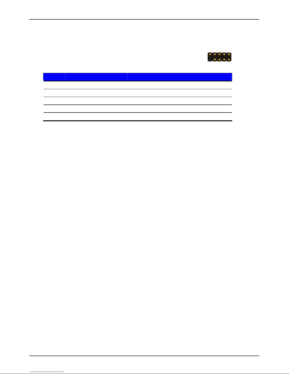
A.9 < USB Interface >
9
1
Connector: J3
Type: 10-pin (5 x 2) header for dual USB Ports
2
10
Pin Description Pin Description
1 VCC 2 VCC
3 Data0- 4 Data15 Data0+ 6 Data1+
7 Ground 8 Ground
9 Ground 10 NC
Page 36

LV-668 User’s Manual
36
(This Page is Left for Blank)
Page 37

LV-668 User’s Manual BIOS Setup
LAN Port
37
Appendix B <Flash BIOS>
B.1 BIOS Auto Flash Tool
The board is based on Award BIOS and can be updated easily by the BIOS auto flash
tool. You can download the tool online at the address below:
http://www.award.com
http://www.commell.com.tw/support/support.htm
File name of the tool is “awdflash.exe”, it’s the utility that can write the data into the BIOS
flash ship and update the BIOS.
B.2 Flash Method
1. Please make a bootable floppy disk.
2. Get the last .bin files you want to update and copy it into the disk.
3. Copy awardflash.exe to the disk.
4. Power on the system and flash the BIOS. (Example: C:/ awardflash XXX.bin)
5. Re-star the system.
Any question about the BIOS re-flash please contact your distributors or visit the
web-site at below:
http://www.commell.com.tw/support/support.htm
Page 38

LV-668 User’s Manual
38
(This Page is Left for Blank)
Page 39
LV-668 User’s Manual System Resources
I/O Port Address Map
39
Appendix C <System Resources>
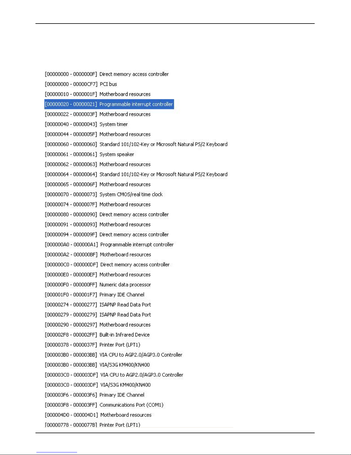
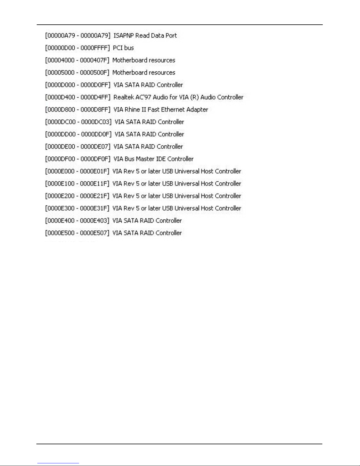
C.1 <I/O Port address Map>
Page 40
LV-668 User’s Manual System Resources
I/O Port Address Map
40
Page 41
LV-668 User’s Manual System Resources
Memory Address Map
41
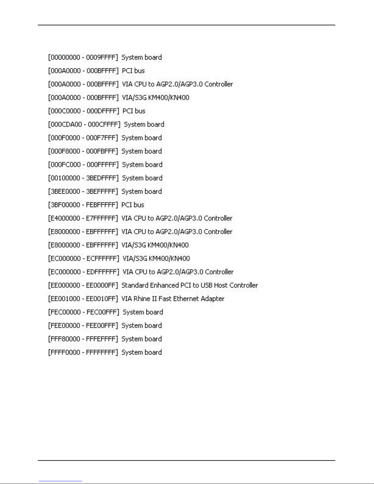
C.2 <Memory Address Map>
Page 42
LV-668 User’s Manual System Resources
IRQ & DMA Resource
42
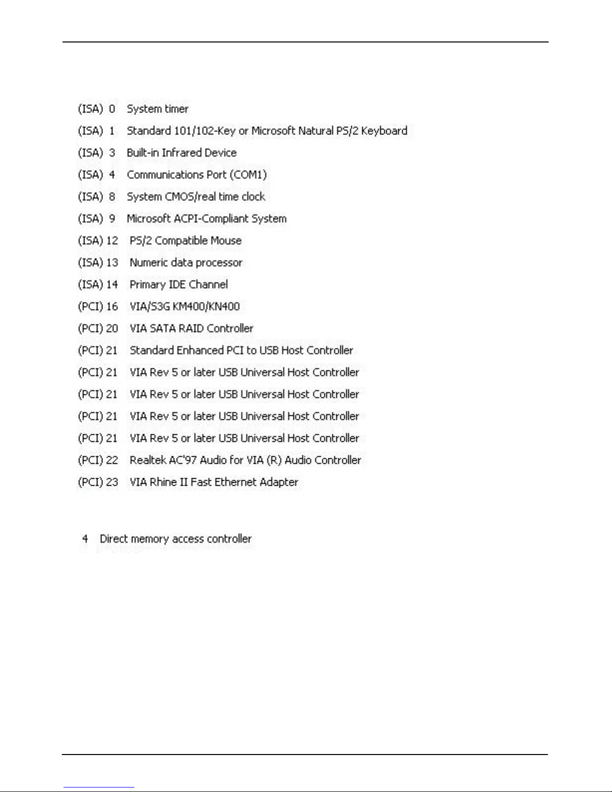
C.3 <System IRQ & DMA Resource>
C.3.1 <IRQ>
<DMA>
Page 43

LV-668 User’s Manual System Resources
IRQ & DMA Resource
43
(This Page is Left for Blank)
Page 44

LV-668 User’s Manual
44
Contact Information
Any advice or comment about our products and service, or anything
we can help you please don’t hesitate to contact with us. We will do
our best to support you for your products,projects and business.
Taiwan Commate Computer Inc.
Address
8F, No. 94, Sec. 1, Shin Tai Wu Rd., Shi Chih
Taipei Hsien, Taiwan
TEL +886-2-26963909
FAX +886-2-26963911
Website
http://www.commell.com.tw
E-Mail
[email protected] (General Information)
[email protected] (Technical Support)
Co
mmell is our tr
adema
rk of in
dustria
l PC division
 Loading...