

Page 1
HE-B71
PICMG 1.3 Half-size CPU Card
User’s Manual
Edition 1.2
2014/10/09
Page 2

HE-B71 User’s Manual
Copyright
Copyright 2014, all rights reserved. This document is copyrighted and all rights are
reserved. The information in this document is subject to change without prior notice t o
make improvements to the products.
This document contains proprietary information and pr otected by copyright. No part of
this document may be reproduced, copied, or translated in any form or any means
without prior written permission of the manufacturer.
All trademarks and/or registered trademarks contains in this document are property of
their respective owners.
Disclaimer
The company shall not be liable for any incidental or consequenti al damages resulting
from the performance or use of this product.
The company does not issue a warranty of any kind, express or implied, including
without limitation implied warranties of merchantability or fitness for a particular
purpose.
The company has the right to revise the manual or include changes in the specifications
of the product described within it at any time without notice and without obli gation to
notify any person of such revision or changes.
Trademark
All trademarks are the property of their respective holders.
Any questions please visit our website at HTUUhttp://www.commell.com.twUTU
Page 3
HE-B71 User’s Manual
(
)
(
)
(
)
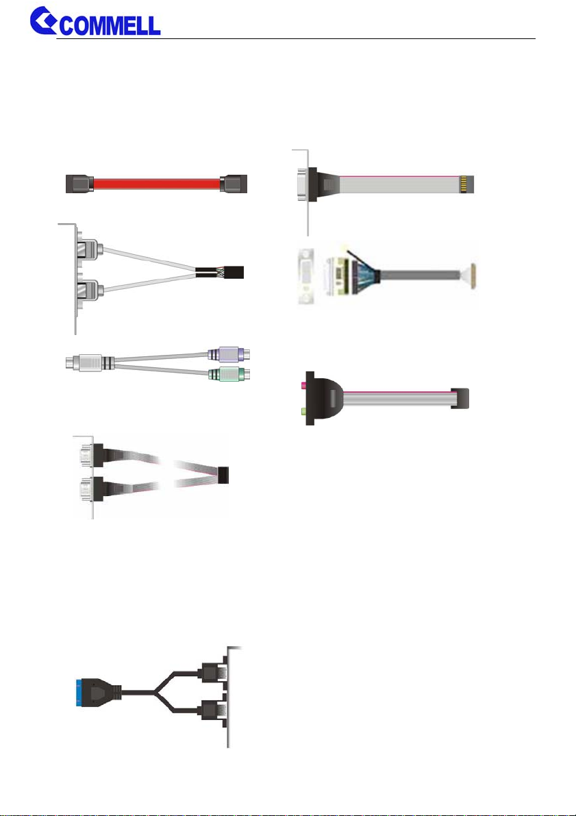
Packing List:
Please check the package content before you starting using the board.
Hardware:
HE-B71 PICMG 1.3 Half-size CPU Card x 1 (include Cooler Fan)
Cable Kit:
SATA Cable x 2
(OALSATA3-L)/ (1040529)
USB2.0 Cable x 1
OALUSBA-1 )/ (1040172
PS/2 Keyboard & Mouse Cable x 1
(OALPS2/MKN)/ (1040551)
Dual COM PORT Cable x 1
OALES-BKU2)/ (1040087
Printed Matters:
Driver CD (Including User’s Manual) x 1
CRT cable x 1
(OALVGA-S-7)/ (1040556)
DVI module with bracket x 1
(BADPDVIP_A&OALDVI-DF13)/
(4120008021 & 1040483)
Audio Cable x 1
(OALPJ-HD)/ (1040120)
Optional :
USB3.0 Cable
OALUSB3)/ (1040531
Page 4

HE-B71 User’s Manual
Index
Chapter 1 <Introduction>..............................................................................1
1.1 <Product Overview>.....................................................................................1
1.2 <Product Specification>................................................................................2
1.3 <Mechanical Drawing>.................................................................................3
1.4 <Block Diagram>..........................................................................................4
Chapter 2 <Hardware Setup>........................................................................5
2.1 <Connector Location>..................................................................................5
2.2 <Jumper Location & Reference>..................................................................6
2.3 <Connector Reference>...............................................................................7
2.3.1 <Internal Connectors> .....................................................................7
2.3.2 <External Connectors>....................................................................7
2.4 <Memory Setup>..........................................................................................8
2.5 <CMOS & ATX Setup>.................................................................................9
2.6 <Serial ATA Interface>................................................................................ 10
2.7 <Ethernet Interface>................................................................................... 11
2.8 <Onboard Display Interface>......................................................................12
2.8.1 <External Display>.........................................................................12
2.8.2 <Internal Display>..........................................................................13
2.9 <Integrated Audio Interface>...................................................................... 18
2.10 <USB Interface>.......................................................................................19
2.11 <Serial Port>.............................................................................................21
2.12 <PCIe Mini Card Interface>...................................................................... 23
2.13 <GPIO and SMBUS Interface>.................................................................24
2.14 <Power Supply and Fan Interface >.........................................................25
2.14.1 <Power Input>(need Backplane)..................................................25
2.14.2 <Fan connector>..........................................................................26
2.15 <Switch and Indicator>.............................................................................27
Chapter 3 <System Setup>.........................................................................28
3.1 <Audio Configuration>................................................................................ 28
Page 5

HE-B71 User’s Manual
3.2 <Display Properties Setting>......................................................................29
3.3 <SATA configuration>.................................................................................31
3.4 <SATA RAID Configuration>.......................................................................32
Chapter 4 <BIOS Setup> .............................................................................34
Appendix A <I/O Port Pin Assignment>.....................................................36
A.1 <Serial ATA Port>.......................................................................................36
A.2 <IrDA Port>................................................................................................36
A.3 <LAN Port>................................................................................................36
A.4 <LPC Port>................................................................................................36
Appendix B <Flash BIOS> ..........................................................................37
B.1 <Flash Tool> ..............................................................................................37
B.2 <Flash BIOS Procedure>...........................................................................37
Appendix C <Programming GPIO’s>.........................................................38
Appendix D <Programming Watchdog Timer >........................................39
Contact Information.....................................................................................40
Page 6

HE-B71 User’s Manual
(This page is left for blank)
Page 7

HE-B71 User’s Manual
Chapter 1 <Introduction>
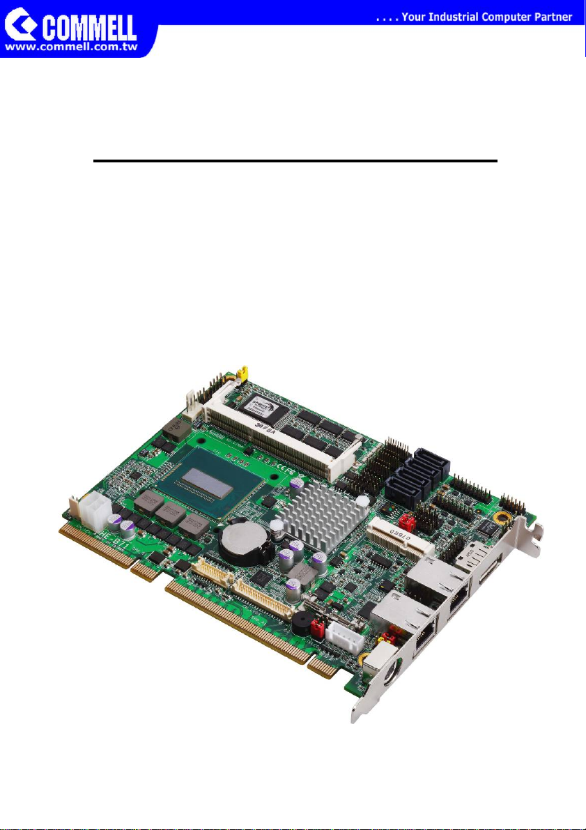
1.1 <Product Overview>
HE-B71 the 4th Generation Intel of the PICMG 1.3 Half-size CPU Card, supports 4th
Generation Intel® Core™ i7, Core™ i5, Core™ i3, Celeron Mobile Processor and
features Intel DH82QM87 chipset, integrated HD Graphics, DDR3L memory, REALTEK
High Definition Audio, Serial ATA with AHCI and RAID function for a system and Intel
Gigabit LAN.
Intel Haswell Bridge Processor
The 4th Generation Intel® Core™ processor family mobile is the next generation of
64-bit, multi-core mobile processor built on 22- nanometer process technology. Based
on a new micro-architecture.
New features for Intel DH82QM87 chipset
The DH82QM87 chipset provides better CPU, graphics, media performance, flexibility
and more enhanced security that is suitable for a variety of intelligent systems the ideal
choice.
All in One multimedia solution
Based on Intel DH82QM87 chipset, the board provides high performance onboard
graphics, CRT, 24-bit dual channel LVDS interface, DisplayPort, DVI and 2.1 channels
High Definition Audio, to meet the very requirement of the multimedia application.
Flexible Extension Interface
The board provides one PCIe mini slot, in addition, the backplane provides one PCIe
x16 slot, one PCIe x4 or four PCIe x1.
-1-
Page 8
HE-B71 User’s Manual
1.2 <Product Specification>
General Specification
Form Factor PICMG 1.3 Half-size CPU Card
CPU 4th Generation Intel® Core™ i7, Core™ i5, Core™ i3, Celeron® Mobile
Processor
Package type: FCBGA1364
Memory 2 x DDR3L SO-DIMM 1333/1600 MHz up to 16GB
Support Non-ECC, unbuffered memory only
Chipset Intel® DH82QM87 PCH
Real Time Clock Chipset integrated RTC with onboard lithium battery
Watchdog Timer Generates a system reset with internal timer for 1min/s ~ 255min/s
Power Management Support ACPI 4.0 compliant
Serial ATA Interface 4 x serial ATA3 interface with 600MB/s transfer rate (Only for SATA3)
Support RAID 0, 1, 5, 10 and Intel Rapid Storage Technology
Display Interface Intel® 4th Generation Core mobile processor integrated HD Graphics 4600
1 x CRT (Onboard 2x8 pin-header)
1 x DVI (Onboard 20-bit connector)
1 x DisplayPort (Rear I/O Port)
1 x LVDS (Onboard 24-bit dual channel connector with +3.3/+5/+12V supply)
Audio Interface Realtek ALC888 HD Audio
LAN Interface 1 x Intel® I210-AT Gigabit LAN
1 x Intel® I217-LM Gigabit LAN (Support iAMT9.0)
GPIO Interface Onboard programmable 12 pin-header, 8-bit Digital I/O interface
Extended Interface PICMG 1.3 Half-size Interface Support 1 PCI-Express x16、1 x PCIe x4 or
4 x PCIe x1, 1 x Mini PCIe slot (Optional support mSATA (Only for SATA3))
Internal I/O Port 1 x RS232/422/485, 5 x RS232, 1 x SMBUS, 1 x GPIO, 4 x USB3.0, 2 x
USB2.0, 1 x IrDA,1 x CRT, 1 x DVI, 1 x LPC, 1 x LVDS, 1 x LCD inverter, 4 x
Serial ATA3 and 1 x Front panel Audio
External I/O Port 2 x LAN, 1 x DisplayPort and 1 x PS/2
Power Requirement Standard 24-pin ATX Power from Backplane
Dimension 168mm x 126mm
Temperature Operating within 0~60 centigrade
Storage within -20~85 centigrade
Ordering Code
Onboard CRT, LVDS, DVI, DisplayPort, SATA3, USB2.0, USB3.0, HD Audio ,LAN , SMBUS, LPC,
SIM, GPIO, IrDA, PS/2, PCIe mini card, mSATA.
HE-B7117L1 i7-4700EQ Mobile Processor, 4 x PCIe x1
HE-B7117L4 i7-4700EQ Mobile Processor, 1 x PCIe x4
HE-B7117P1 Celeron 2002E Mobile Processor, 4 x PCIe x1
HE-B7117P4 Celeron 2002E Mobile Processor, 1 x PCIe x4
The specifications may be different as the actual production.
For further product information please visit the website at
HTUUhttp://www.commell.com.twUTUH
-2-
Page 9
HE-B71 User’s Manual
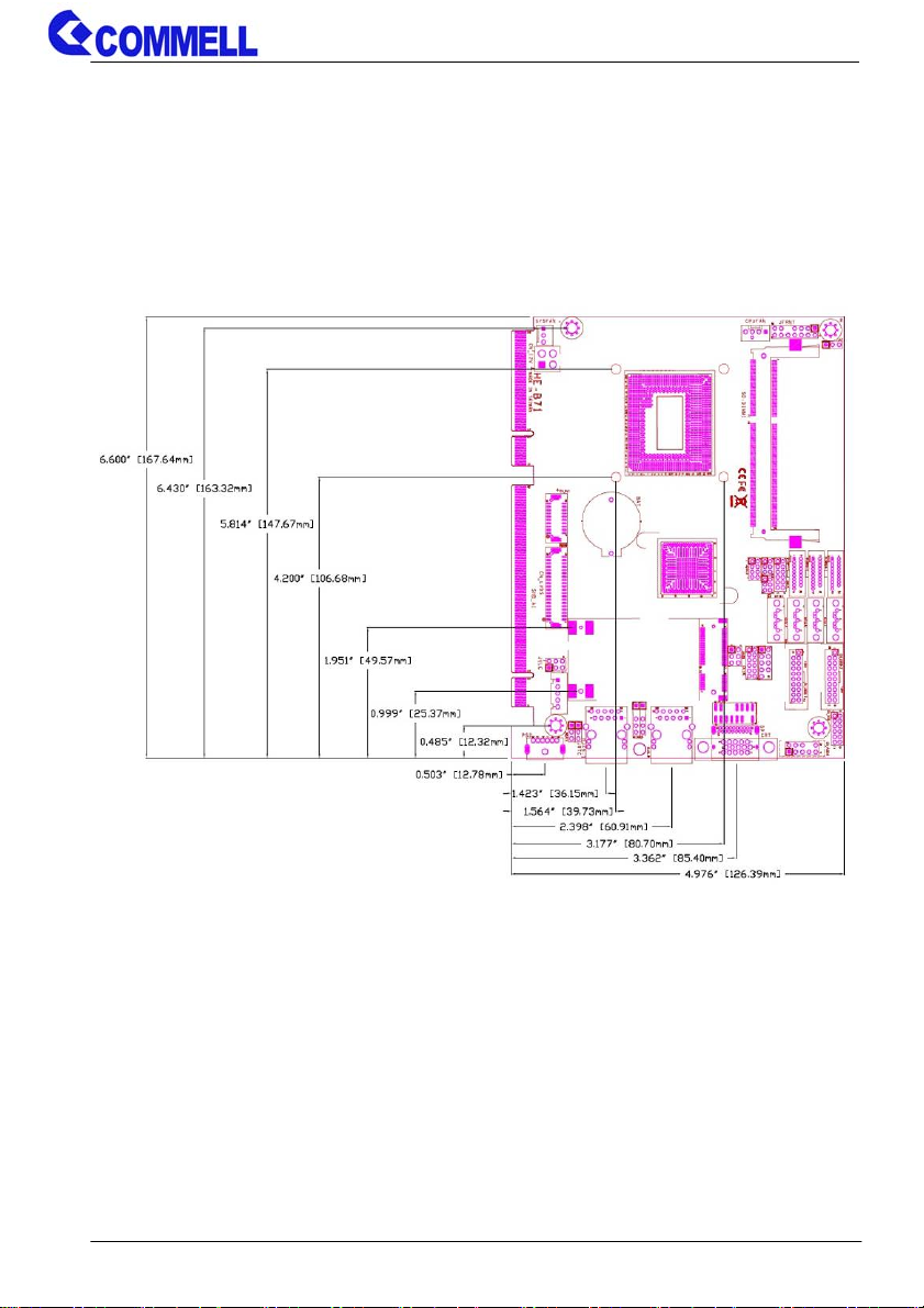
1.3 <Mechanical Drawing>
-3-
Page 10
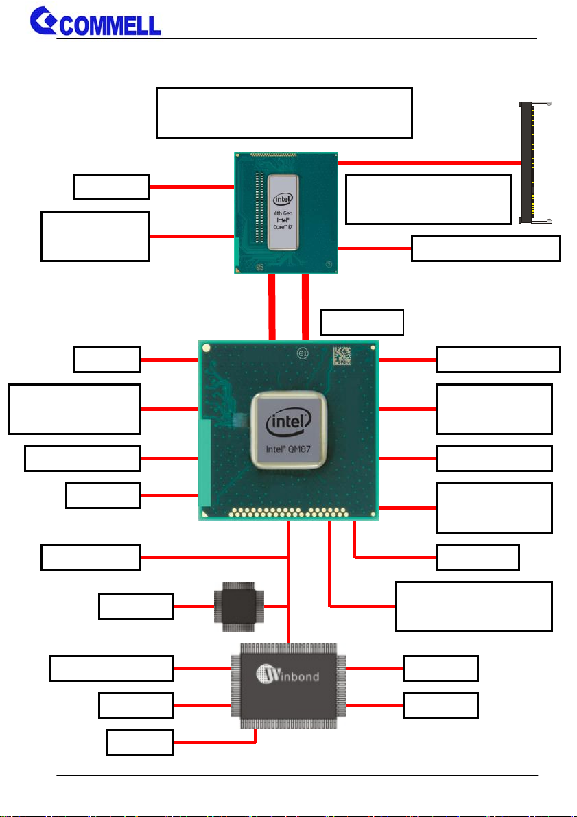
1.4 <Block Diagram>
HE-B71 User’s Manual
Channel A
2 x DDR3L SO-DIMM
1333/1600 MHz up to 16GB
PCI-E x16
1 x PCIe X16(Backplane)
1 x LVDS
1 x DisplayPort
1 x DVI
4th Generation Intel® Core™ i7, Core™
i5, Core™ i3, Celeron Mobile Processor
eDP
DDI
1 x CRT
CRT PCI-E x1
FDI DMI
DH82QM87
1 x PCI-E mini card
4 x SATA3
(Not support SATA2)
SATA3
ALC888 HD Audio
SPI Flash
SPI
1 x LPC(TPM)
LPC
USB3.0
USB2.0
PCI-E x1
2 x External USB
2 x Internal USB
2 x Internal USB
1 x Intel® I217-LM
1 x Intel® I210-AT
1 x SMBUS
5 x RS232
F81216D
1 x PCIe X4 or 4 x PCIe X1
(Backplane)
1 x RS232/422/485
1 x RS232
1 x PS/2
W83627DHG-P
1 x GPIO
1 x IrDA
-4-
Page 11
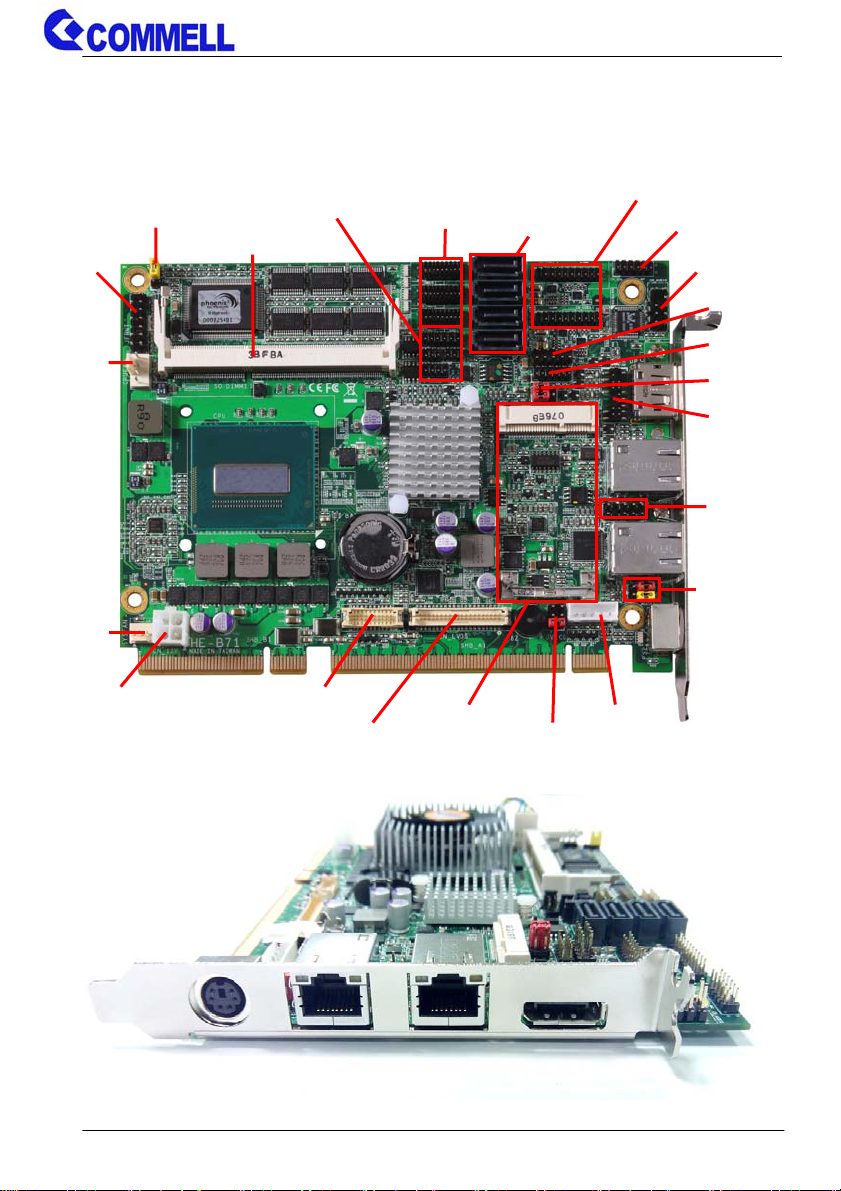
Chapter 2 <Hardware Setup>
2.1 <Connector Location>
JFRNT
CPUFAN
SYSFAN
JAT
SO-DIMM1
HE-B71 User’s Manual
JCSEL1
JP1 JP2
JCSEL2
CN_COM5/6
CN_COM3/4
CN_COM1/2
SATA3-4
SATA3-3
SATA3-2
SATA3-1
CN_USB3-2
CN_USB3-1
CN_DIO
CN_AUDIO
CN_USB2
CN_LPC
JVUSB
CN_CRT
CN_IR
CN_SMBUS
JRTC
JMSATA
CN_12V
CN_DVI
CN_LVDS
MINI_CARD
CN_INV
JVLCD
PS/2 RJ45-1 RJ45-2 DisplayPort
-5-
Page 12
HE-B71 User’s Manual
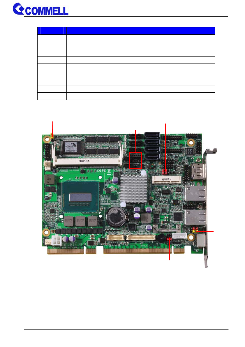
2.2 <Jumper Location & Reference>
Jumper Function
JRTC CMOS Operating/Clear Setting
JVLCD Panel Voltage Setting
JAT Power mode select
JP1 Com1 Voltage Setting (For Pin 9)
JP2 Com2 Voltage Setting (For Pin 9)
JCSEL1
JCSEL2
JVUSB
JMSATA
JAT
CN_COM2 RS-232 RS422 RS485 Setting
CN_IR IrDA Setting
USB Voltage Setting
Mini Card mSATA Setting
JCSEL1
JP1 JP2
JCSEL2
JVUSB
-6-
JRTC
JMSATA
JVLCD
Page 13
HE-B71 User’s Manual
2.3 <Connector Reference>
2.3.1 <Internal Connectors>
Connector Function Remark
CPU FCBGA 1364 CPU
SO-DIMM 1/2 204 -pin DDR3L SO-DIMM slot
SATA 1/2/3/4 7-pin Serial ATA3 connector
CN_12V DC 12V input connector
CN_AUDIO 5 x 2-pin audio connector
CN_DIO 6 x 2-pin digital I/O connector
CN_USB2 5 x 2-pin USB2.0 connector
CN_USB3-1/2 10 x 2-pin USB3.0 connector
CPUFAN 4-pin CPU cooler fan connector
SYSFAN 3-pin System cooler fan connector
CN_CRT 8 x 2-pin CRT connector
CN_DVI 10 x 2-pin DVI connector
CN_LVDS 20 x 2-pin LVDS connector
CN_INV 5-pin LCD inverter connector
CN_IR 5-pi n IrDA connector
CN_COM1/2 19-pin RS232/485/422 for COM2
CN_COM3/4, 5/6 10 x 2-pin RS232
CN_LPC 6 x 2-pin LPC connector
CN_SMBUS 5-pin SMBUS connector
JFRNT
Mini-PCIe 52-pin Mini-PCIe slot
7 x 2-pin front panel switch/indicator
connector
2.3.2 <External Connectors>
Connector Function Remark
DisplayPort 20-pin DisplayPort connector
PS/2 PS/2 keyboard and mouse co nnector
RJ45-1/2 RJ45 LAN connector
-7-
Page 14
HE-B71 User’s Manual
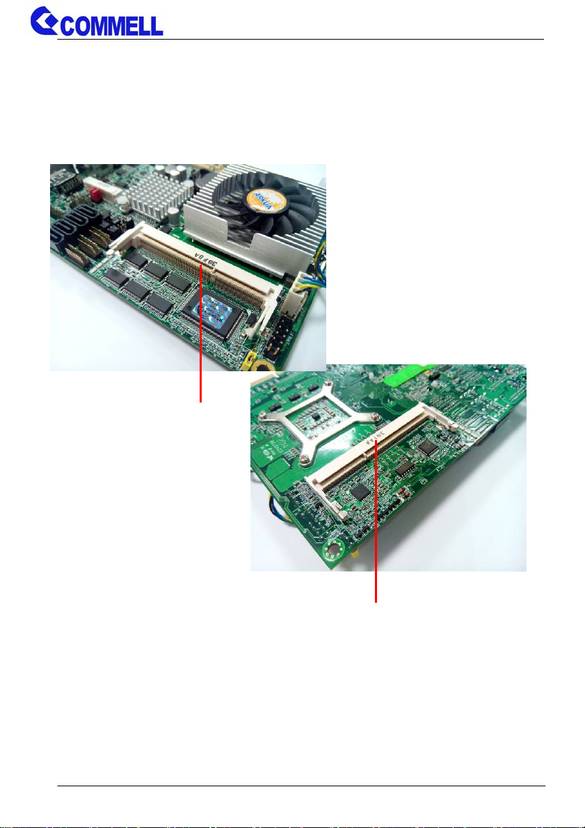
2.4 <Memory Setup>
The board provides 2 x 204-pin DDR3L SO-DIMM to support 1333/1600MHz up to
16GB. Support Non-ECC, unbuffered memory only.
SO-DIMM1
SO-DIMM2
-8-
Page 15

HE-B71 User’s Manual
2.5 <CMOS & ATX Setup>
The board’s data of CMOS can be setting in BIOS. If the board refuses to boot due to
inappropriate CMOS settings, here is how to proceed to clear (reset) the CMOS to its
default values.
Jumper: JRTC
Type: Onboard 3-pin jumper
JRTC Mode
1-2 Clear CMOS
2-3 Normal Operation
Default setting: 2-3
Jumper: JAT
Type: Onboard 3-pin jumper
JAT Mode
1-2 AT Mode
2-3 ATX Mode
Default setting:2-3
3
1
JAT
JRTC
1 3
-9-
Page 16

HE-B71 User’s Manual
2.6 <Serial ATA Interface>
HE-B71 has Four Serial ATA 3 interfaces with RAID function, the transfer rate of the
Serial ATA 3 can be up to 600MB/s. Please go to
HUhttp://www.serialata.org/UH for more
about Serial ATA technology information. The main features on Intel® QM87 PCH are
listed below:
1. Optimizing performance of the computer, the reaction speed and reliability
2. Intel® Smart Response Technology for fast access to frequently used files and
applications.
3. Superior performance and data protection: RAID technology
4. Dynamic Storage Accelerator release SSD performance power
5. Intel® Rapid Recover Technology provides fast data recovery
6. Lower power consumption and more excellent performance and flexibility
Based on Intel® PCH, it supports Intel® Rapid Storage Technology with combination
of RAID 0,1,5 and 10.
1. Supports for up to RAID volumes on a single, two-hard drive RAID array.
2. Supports for Serial ATA ATAPI devices.
3. Supports for RAID spares and automatic rebuild.
4. Supports on RAID arrays, including NCQ and native hot plug.
For more information please visit Intel’s official website.
For more about the system setup for Serial ATA, please check the chapter of SATA
configuration.
SATA3-4
SATA3-3
SATA3-2
SATA3-1
-10-
Page 17

HE-B71 User’s Manual
2.7 <Ethernet Interface>
The board integrates with one Intel® I210-AT Gigabit Ethernet & Intel® I217-LM
controllers, The Intel Gigabit Ethernet supports triple speed of 10/100/1000Base-T, with
IEEE802.3 compliance.
Onboard Intel® I217-LM GbE controller support Intel® AMT 9.0 feature on primary LAN
port. The BIOS is ready to support Intel® AMT 9.0 feature. The necessary prerequisite
is your CPU must support Intel® vPro technology, ex. HUi7-4700EQU
For further instruction about the Intel® AMT features and set up, please refer to the
I210-AT I217-LM
iAMT Setting.pdf.
-11-
Page 18

HE-B71 User’s Manual
2.8 <Onboard Display Interface>
Based on Intel Haswell Bridge CPU with built-in HD Graphic, the board provide one
DisplayPort on the external I/O port, one 40-pin LVDS interface with 5-pin LCD backlight
inverter connector, one internal 16-pin CRT and 20-pin DVI connector interface .
The board provides triple display function with clone mode and extended desktop mo de
for DVI, DisplayPort, CRT and LVDS.
2.8.1 <External Display>
Please connect your monitor which supports DisplayPort to connect onboard rear
I/O Port.
DisplayPort
-12-
Page 19

HE-B71 User’s Manual
2.8.2 <Internal Display>
The board provides one 16-pin CRT, 20-pin DVI and 40-pin LVDS connector for 24-bit
single/dual channel panels, the LVDS supports up to 2048 x 1536 (UXGA) resolution,
with one LCD backlight inverter connector and one jumper for panel voltage setting.
CN_CRT
1 2
16 15
CN_DVI
2
1
40
39
CN_LVDS
2
1
20
19
JVLCD
6 5
2 1
1 5
CN_INV
Effective patterns of connection: 1-2 / 3-4 / 5-6
4 3
6 5
1 2
Warning: others cause damages
-13-
Page 20

HE-B71 User’s Manual
Connector: CN_CRT
Connector type: 16-pin header connector (pitch = 2.00mm)
Pin Number Assignment Pin Number Assignment
1 BR 2 BG
3 BB 4 NC
5 -CRTATCH 6 IOGND1
7 IOGND1 8 IOGND1
9 NC 10 -CRTATCH
11 NC 12 5VCDA
13 5HSYNC 14 5VSYNC
15 5VCLK 16 NC
Connector: CN_INV Connector: JVLCD
Type: 5-pin LVDS Power Header Type: 6-pin Power select Header
Pin Description
1 +12V
2 Reserved (Note)
3 GND
4 GND
5 ENABKL
Note: Reserved for MB internal test
Please treat it as NC.
Connector: CN_DVI
Connector type: onboard 20-pin connector
Pin Number Assignment Pin Number Assignment
1 +5V 2 N/C
3 HPD 4 Ground
5 TMDSTX0N 6 TMDSTX0P
7 Ground 8 TMDSTX1N
9 TMDSTX1P 10 Ground
11 TMDSTX2N 12 TMDSTX2P
13 Ground 14 Ground
15 TMDSTXCP 16 Ground
17 DVI_DA 18 DVI_SL
19 N/C 20 N/C
Pin Description
1-2 LCDVCC (3.3V)
3-4 LCDVCC (5V)
5-6 LCDVCC (12V)
Default: 1-2
-14-
Page 21

HE-B71 User’s Manual
Connector: CN_LVDS
Type: onboard 40-pin connector
Connector model:
E&T 3950-B40C-00R or similar (HIROSE DF13-40DP-1.25V compatible)
Pin Signal Pin Signal
2 LCDVCC 1 LCDVCC
4 GND 3 GND
6 ATX0- 5 BTX0-
8 ATX0+ 7 BTX0+
10 GND 9 GND
12 ATX1- 11 BTX114 ATX1+ 13 BTX1+
16 GND 15 GND
18 ATX2- 17 BTX220 ATX2+ 19 BTX2+
22 GND 21 GND
24 ACLK- 23 BTX326 ACLK+ 25 BTX3+
28 GND 27 GND
30 ATX3- 29 BCLK32 ATX3+ 31 BCLK+
34 GND 33 GND
36 DDCPCLK 35 SMBCKL
38 DDCPDATA 37 SMBDATA
40 N/C 39 SPDIFO
-15-
Page 22

HE-B71 User’s Manual
To setup the LCD, you need the component below:
1. A panel with LVDS interfaces.
2. An inverter for panel’s backlight power.
3. A LCD cable and an inverter cable.
For the cables, please follow the pin assignment of the conne ctor to mak e a cable, be cause
every panel has its own pin assignment, so we do not pro vide a s tandard cable; please fi nd
a local cable manufacture to make cables.
LCD Installation Guide:
1. Preparing the HE-B71, LCD panel and the backlight inverter.
2. Please check the datasheet of the panel to see the voltage of the panel, and set
the jumper JVLCD to +12V or +5V or +3.3V.
3. You would need a LVDS type cable.
Panel side
For sample illustrator only
4. To connect all of the devices well.
-16-
Board side
Page 23

HE-B71 User’s Manual
After setup the devices well, you need to select the LCD panel type in the BIOS.
The panel type mapping is list below:
BIOS panel type selection form (BIOS Version:1.0)
Single / Dual channel Single / Dual channel
NO. Output format NO. Output format
1 640 x 480 9 1680 x 1050
2 800 x 600 10 1920 x 1200
3 1024 x 768 11 1440 x 900
4 1280 x 1024 12 1024 x 768
5 1400 x 1050 Reduced Blanking 13 1280 x 1024
6 1400 x 1050 non-Reduced Blanking 14 1280 x 800
7 1680 x 1200 15 1920 x 1080
8 1366 x 768 16 2048 x 1536
-17-
Page 24

HE-B71 User’s Manual
2.9 <Integrated Audio Interface>
The board provides the onboard high definition audio with Realtek ALC888
Connector: CN_AUDIO
Type: 10-pin (2 x 5) 1.27mm x 2.54mm-pitch header
Pin Description Pin Description
1 MIC_L 2 Ground
3 MIC_R 4 N/C
5 Speaker_R 6 MIC Detect
7 SENSE 8 N/C
9 Speaker_L 10 Speaker Detect
9
10
12
9 10
2 1
CN_AUDIO
-18-
Page 25

HE-B71 User’s Manual
2.10 <USB Interface>
HE-B71 integrates four USB3.0 ports and two USB2.0 ports.
The specifications of USB3.0 are listed below:
Interface USB3.0
Controller
Transfer Rate Up to 5Gb/s
Voltage 5V
The specifications of USB2.0 are list
Interface USB2.0
Controller
Transfer Rate Up to 480Mb/s
Voltage 5V
Intel®QM87
Intel®QM87
CN_USB3-1/2
Type: USB3.0
1 10
20 11
CN_USB2
Type: USB2.0
2 10
-19-
1 9
JVUSB
2 6
1 5
Page 26

Connector: CN_USB3
HE-B71 User’s Manual
Type: 20-pin (2 x 10) header (pitch = 2.0mm)
Pin Description Pin Description
1 VCC 20 NC
2 USB3.0_RX0- 19 VCC
3 USB3.0_RX0+ 18 USB3.0_RX14 Ground 17 USB3.0_RX1+
5 USB3.0_TX0- 16 Ground
6 USB3.0_TX0+ 15 USB3.0_TX17 Ground 14 USB3.0_TX1+
8 Data0- 13 Ground
9 Data0+ 12 Data110 NC 11 Data1+
Connector: CN_USB2
Type: 10-pin (2 x 5) header (pitch = 2.54mm)
Pin Description Pin Description
1 VCC 2 VCC
3 Data0- 4 Data15 Data0+ 6 Data1+
7 Ground 8 Ground
9 Ground 10 N/C
Connector: JVUSB
Type: 6-pin Power select jumper
Pin Description
1-3 & 2-4 5V_SB
3-5 & 4-6 5V
Default: 1-3 & 2-4
Effective patterns of connection: 1-3 & 2-4 or 3-5 & 4-6
2
1
6
5
Warning: others cause damages
2
1
6
5
-20-
Page 27

HE-B71 User’s Manual
2.11 <Serial Port>
The board supports five RS232 serial port and one jumper selectable RS232/422/485
serial ports. The jumper JCSEL1 & JCSEL2 can let you configure the communicating
modes for COM2.
Connector: COM1/2
Type: 20-pin(2 x 10)header pitch = 2.54 x 1.27mm
Pin Description Pin Description
1 DCD1 2 RXD1
3 TXD1 4 DTR1
5 GND1 6 DSR1
7 RTS1 8 CTS1
9 RI1 10 N/C
11 DCD2/422TX-/485- 12 RXD2/422TX+/485+
13 TXD2/422RX+ 14 DTR2/422RX15 GND 16 DSR2
17 RTS2 18 CTS2
19 RI2 20 N/C
Setting RS-232 & RS-422 & RS-485 for COM2
Connector: COM3/4, 5/6
Type: 20-pin(2 x 10)header pitch = 2.54 x 1.27mm
Pin Description Pin Description
1 DCD1 2 RXD1
3 TXD1 4 DTR1
5 GND1 6 DSR1
7 RTS1 8 CTS1
9 RI1 10 N/C
11 DCD2 12 RXD2
13 TXD2 14 DTR2
15 GND2 16 DSR2
17 RTS2 18 CTS2
19 RI2 20 N/C
-21-
Page 28

HE-B71 User’s Manual
Jumper: JCSEL1,JCSEL2
Type: 12-pin (6 x 2) & 8-pin (4 x 2) for set COM2 mode jumper
RS232 RS485 RS422 IrDA
JCSEL1
JCSEL2
Default: RS232
JP1
2 6
1 5
Jumper: JP1/JP2 (COM1/2)
Type: onboard 6-pin header
COM1/2, 3/4, 5/6
2 20
1 19
JCSEL1
2 12
1 11
JP2
2 6
1 5
JCSEL2
2 8
1 7
Power Mode JP1/2
Pin 9 with 5V Power 1-2
Pin 9 with 12V Power 3-4
Standard COM port 5-6
Default setting (5-6)
-22-
Page 29

HE-B71 User’s Manual
2.12 <PCIe Mini Card Interface>
The board provides one PCIe mini card slot.
MINI_CARD can selectively support mSATA.
Connector: JMSATA
Type: onboard 3-pin header
JMSATA Mode
1-2 Support mSATA for MINI_CARD1
2-3 Support PCIe and USB
Default setting: 2-3
JMSATA
1 3
MINI_CARD
-23-
Page 30

HE-B71 User’s Manual
2.13 <GPIO and SMBUS Interface>
The board provides a programmable 8-bit digital I/O interface; you can use this general
purpose I/O port for system control like POS or KIOSK. The GPIO is an Open-drain
output and TTL-level input.
1. Output:Open-drain, Most applications need use an external pull-up resistor.
2. Input:TTL-level.
DC characteristics:
Parmeter SYM MIN TYP MAX UNIT Conditions
Input Low Voltage VIL 0.8 V
Input High Voltage VIH 2.0 V
Output Low Voltage V
Input High Leakage I
Input Low Leakage I
LIH
LIL
Connector: CN_DIO
Type: 12-pin (6 x 2) header (pitch = 2.0mm)
Pin Description Pin Description
1 Ground 2 Ground
3 GPIO1 4 GPIO5
5 GPIO2 6 GPIO6
7 GPIO3 8 GPIO7
9 GPIO4 10 GPIO8
11 5V 12 12V
Connector: CN_SMBUS
Type: 5-pin header for SMBUS Ports
Pin Description
1 VCC
2 N/C
3 SMBDATA
4 SMBCLK
5 Ground
0.4 V IOL =12mA
OL
+10 μA VIN =3.3V
-10 μA VIN =0V
CN_DIO
2
1
12
11
1 5
CN_SMBUS
-24-
Page 31

HE-B71 User’s Manual
2.14 <Power Supply and Fan Interface >
The HE-B71 needs a standard ATX power supply from Backplane's +12V , 5VSB &
3VSB and the board provides one 4-pin fan connector supports smart fan for CPU
cooler and one 3-pin cooler fan connectors for system and Northbridge chip. Please
connect this well before you finishing the system setup.
2.14.1 <Power Input>(need Backplane)
Connector: CN_12V
Type: 4-pin DC power connector
Pin Description Pin Description
1 Ground 2 Ground
3 +12V 4 +12V
4 3
2 1
CN_12V
-25-
Page 32

HE-B71 User’s Manual
2.14.2 <Fan connector>
The board provides one 4-pin fan connecto rs supporting smart fan for CPU cooler and
one 3-pin cooler fan connectors for system.
CPUFAN
1
4
SYSFAN
1 3
Connector: CPUFAN
Type: 4-pin fan wafer connector
Pin Description Pin Description
1 Ground 2 +12V
3 Fan Speed Detection 4 Fan Control
Connector: SYSFAN
Type: 3-pin fan wafer connector
Pin Description Pin Description Pin Description
1 Ground 2 +12V 3 Sense
-26-
Page 33

HE-B71 User’s Manual
2.15 <Switch and Indicator>
The JFRNT provides front control panel of the board, such as power button, reset and
beeper, etc. Please check well before you connecting the cables on the chassis.
Connector: JFRNT
Type: onboard 14-pin (2 x 7) 2.54-pitch header
Function Signal PIN Signal Function
IDE LED
Reset
Power
Button
HDLED+ 1 2 PWRLED+
PWRBT+ 11 12 N/C
PWRBT- 13 14 SPK-
JFRNT
1 2
13 14
HDLED- 3 4 N/C
Power
LED
Reset+ 5 6 PWRLED-
Reset- 7 8 SPK+
N/C 9 10 N/C
Speaker
-27-
Page 34

HE-B71 User’s Manual
Chapter 3 <System Setup>
3.1 <Audio Configuration>
The board integrates Intel® QM87 with REALTEK® ALC888 codec. It can support
2-channel sound under system configuration. Please follow the steps belo w to setup
your sound system.
1. Install REALTEK HD Audio driver.
2. Launch the control panel and click Sound.
3. Select Speaker Configuration.
-28-
Page 35

HE-B71 User’s Manual
3.2 <Display Properties Setting>
Based on Intel QM87 with HD Graphic, the board supports two DACs for display device
as different resolution and color bit.
Please install the Intel Graphic Driver before you starting setup display devices.
1. Click right button on desktop to launch “Screen resolution” and click Ad vanced
settings, or click the “Graphics Properties…” directly into the Intel(R) HD Graphics
Control Panel.
2. Click Intel(R) HD Graphics Control Panel button for more setup.
Click Graphics Properties... for
advanced setup
-29-
Page 36

HE-B71 User’s Manual
3. This setup options can let you define each device settings.
Click Display Settings to setup
the monitor for Resolution and
Refresh Rate
Click Multiple Displays to setup the
triple display mode as same screen
-30-
Page 37

HE-B71 User’s Manual
3.3 <SATA configuration>
SA TA Mode:
This option can let you select whether the Serial ATA hard drives would work under
normal IDE mode, AHCI mode or RAID mode. The RAID mode requires more than one
HDD before use.
-31-
Page 38

HE-B71 User’s Manual
3.4 <SATA RAID Configuration>
The board integrates Intel® QM87 PCH with RAID function for Serial ATA drives, and
supports the configurations below:
RAID 0 (Stripping): Two hard drives operating as one drive for optimized d ata R/W
performance. It needs two unused drives to build this operation.
RAID 1 (Mirroring): Copies the data from first drive to second drive for data security,
and if one drive fails, the system would access the applications to the workable drive. It
needs two unused drives or one used and one unused driv e to build this o peration. The
second drive must be the same or lager size than first one.
RAID 5 (striping with parity)
A RAID 5 array contains three or more hard drives where the data is divided into
manageable blocks called strips. Parity is a mathematical method for recreating data
that was lost from a single drive, which increases fault-tolerance. T he data and parity
are striped across all the hard drives in the array. The parit y is striped in a rotating
sequence to reduce bottlenecks associated with the parity calculations.
RAID 10 (RAID 0+1)
A RAID 10 array uses four hard drives to create a combination of RAID levels 0 and 1.
The data is striped across a two-drive array forming the RAID 0 component. Each of the
drives in the RAID 0 array is then mirrored by a RAID 1 component.
Intel Rapid Storage Technology: This technology would allow you to use RAID 0+1
mode on only two drives (4 drives needed on traditional RAID 0+1). It will create t wo
partitions on each hard drive to simulate RAID 0 and RAID 1. It also can let you modify
the partition size without re-formatted.
For more information of Intel Rapid Storage Technology, please visit Intel’s website.
If you need to install an operation system on the RAID set, please use the driver disk
attached in the package when it informs you to obtain the RAID drivers.
-32-
Page 39

HE-B71 User’s Manual
When you boot, press <CTRL+I> to enter the RAID configuration menu.
If you are installing Windows 7, when the installation is complete, please install the
Intel® Rapid Storage Technology.
If you are installing Windows XP, first, you need to install the RAID driver in the
installation screen (need a floppy disk).
-33-
Page 40

HE-B71 User’s Manual
Chapter 4 <BIOS Setup>
The motherboard uses the Phoenix BIOS for the system configuration. The Phoenix
BIOS in the single board computer is a customized version of the industrial standar d
BIOS for IBM PC AT-compatible computers. It supports Intel x86 and compatible CPU
architecture based processors and computers. The BIOS provides critical low-level
support for the system central processing, memory and I/O sub-systems.
The BIOS setup program of the single board computer let the customers modify the
basic configuration setting. The settings are stored in a dedicated battery-backed
memory, NVRAM, retains the information when the power is turned off. If the battery
runs out of the power, then the settings of BIOS will come back to the default setting.
The BIOS section of the manual is subject to change without notice and is provided here
for reference purpose only. The settings and configurations of the BIOS are current at
the time of print, and therefore they may not be exactly the same as that displayed on
your screen.
To activate CMOS Setup program, press <DEL> key immediatel y after you turn on
the system. The following message “Press DEL to enter SETUP” should appear in the
lower left hand corner of your screen. When you enter the CMOS Setup Utility, the Main
Menu will be displayed as Figure 4-1. You can use arrow keys to select your function,
press <Enter> key to accept the selection and enter the sub-menu.
Figure 4-1 CMOS Setup Utility Main Screen
-34-
Page 41

HE-B71 User’s Manual
(This page is left for blank)
-35-
Page 42

HE-B71 User’s Manual
”
Appendix A <I/O Port Pin Assignment>
A.1 <Serial ATA Port>
Connector: SATA3
Type: 7-pin wafer connector
1 2 3 4 5 6 7
GND RSATA_TXP1 RSATA_TXN1 GND RSATA_RXN1 RSATA_RXP1 GND
7 1
A.2 <IrDA Port>
Connector: CN_IR
Type: 5-pin header for SIR Ports
Pin Description
1 VCC
2 N/C
3 IRRX
4 Ground
5 IRTX
JCSEL1 must jump to “SIR
1
5
A.3 <LAN Port>
Connector: RJ45
Type: RJ45 connector with LED on bracket
Pin 1 2 3 4 5 6 7 8
8 1
Description MI0+ MI0- MI1+ MI2+ MI2- MI1- MI3+ MI3-
2
12
A.4 <LPC Port>
Connector: CN_LPC
Type: 10-pin header for LPC Port
Pin Description Pin Description
1 LPC_CLK 2 RESET3 -LFRAME 4 LAD3
5 LAD2 6 LAD1
7 LAD0 8 +3.3V
9 SERIRQ 10 Ground
11 3.3V 12 N/C
-36-
1
11
Page 43

HE-B71 User’s Manual
Appendix B <Flash BIOS>
B.1 <Flash Tool>
The board is based on Phoenix BIOS and can be updated easily by the BIOS auto
flash tool. You can download the tool online at the address below:
HUhttp://www.phoenix.com/en/home/U
HUhttp://www.commell.com.tw/Support/Support_SBC.htmU
File name of the tool is “Fpt.exe”, it’s the utility that can write the data into the BIOS
flash ship and update the BIOS.
B.2 <Flash BIOS Procedure>
1. Please make a bootable floppy disk.
2. Get the last .bin files you want to update and copy it into the disk.
3. Copy Phlash16.exe to the disk.
4. Power on the system and flash the BIOS.
(Example: C:/fpt –savemac –f XXX.bin)
5. Restart the system.
Any question about the BIOS re-flash please contact your distributors or visit the
web-site at below:
HUhttp://www.commell.com.tw/support/support.htmUTU
-37-
Page 44

HE-B71 User’s Manual
Appendix C <Programming GPIO’s>
The GPIO’can be programmed with the MSDOS debug program using
simple IN/OUT commands.The following lines show an example how to
do this. The DC character please refer to GPIO paragraph(Pa ge24).
GPIO0…..GPIO7 bit0……bit7
-o 2E 87 ;enter configuration
-o 2E 87
-o 2E 07
-o 2F 09 ;enale GPIO function
-o 2E 30
-o 2F 02 ;enable GPIO configuration
-o 2E F0
-o 2F xx ;set GPIO as input/output; set ‘1’ for input,’0’for
output
-o 2E F1
-o 2F xx ;if set GPIO’s as output,in this register its value can
be set
Optional :
-o 2E F2
-o 2F xx ; Data inversion register ; ‘1’ inverts the current valus
of the bits ,’0’ leaves them as they are
-o 2E 30
-o 2F 01 ; active GPIO’s
For further information, please refer to Winbond W83627DHG datasheet.
-38-
Page 45

HE-B71 User’s Manual
Appendix D <Programming Watchdog Timer >
The watchdog timer makes the system auto-reset while it stops to work for a period.
The integrated watchdog timer can be setup as system reset mode by program.
Timeout Value Range
- 1 to 255
- Second or Minute
Program Sample
Watchdog timer setup as system reset with 5 second of timeout
2E, 87
2E, 87
2E, 07
2F, 08 Logical Device 8
2E, 30 Activate
2F, 01
2E, F5 Set as Second*
2F, 00
2E, F6 Set as 5
2F, 05
* Minute: bit 3 = 1; Second: bit 3 = 0
You can select Timer setting in the BIOS, after setting the time options, the system
will reset according to the period of your selection.
-39-
Page 46

HE-B71 User’s Manual
Contact Information
Any advice or comment about our products and service, or
anything we can help you please don’t hesitate to contact with us.
We will do our best to support you for your products, projects and
business.
Taiwan Commate Computer Inc.
19F., No.94, Sec. 1, Xintai 5th Rd., Xizhi Dist., New Taipei City
Address
TEL +886-2-26963909
FAX +886-2-26963911
22102, Taiwan
Website
E-Mail
Facebook https://www.facebook.com/pages/Taiwan-Commate-Computer-Inc/547993955271899
Twitter https://twitter.com/Taiwan_Commate
HTUUhttp://www.commell.com.twUTUH
HTUUinfo@commell.com.twUTUH (General Information)
HTUUtech@commell.com.twUTUH (Technical Support)
Commell is a brand name of Taiwan commate computer Inc.
-40-
 Loading...