

Page 1
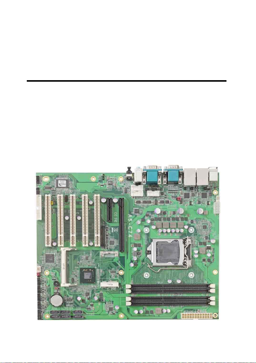
AS-C74
ATX motherboard
User’s Manual
Edition: 1.4
2014/05/13
Page 2

AS-C74 User’s Manual
Copyright
Copyright 2011 All rights reserved. This document is copyrighted and all rights are reserved.
The information in this document is subject to change without prior notice to make
improvements to the products.
This document contains proprietary information and protect ed by copyright. No part of this
document may be reproduced, copied, or translated in any form or any means without prior
written permission of the manufacturer.
All trademarks and/or registered trademarks contains in this document are propert y of their
respective owners.
Disclaimer
The company shall not be liable for any incidental or consequenti al dam ages res ultin g from
the performance or use of this product.
The company does not issue a warranty of any kind, e xpress or implied, including without
limitation implied warranties of merchantability or fitness for a particular purpose.
The company has the right to revise the manual or include changes in th e specifications of
the product described within it at any time without notice and without obligation to notify any
person of such revision or changes.
Trademark
All trademarks are the property of their respective holders.
Any questions please visit our website at TUhttp://www.commell.com.twUT.
2
Page 3
AS-C74 User’s Manual
Packing List
Please check package component before you use our products.
Hardware:
AS-C74 ATX motherboard x 1
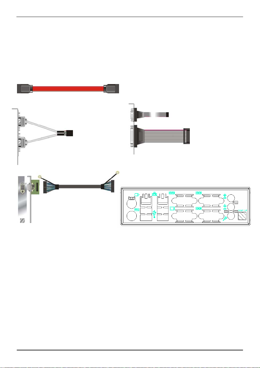
Cable Kit:
SATA Cable x 2
(OALSATA3-L)/ (1040529)
USB Cable x 1(Option)
(OALUSBA-1)/ (1040172)
DB25 & DB9 cable x 1
(OAL1S1P)/ (1040041)
DVI module with bracket x 1
(BADPDVIP_A & OALDVI-P)/
412
21 14
7
I/O Shield x 1
(OPLATE-C74)/ (1270049)
Other Accessories:
Drivers CD (including User’s Manual) x 1
3
Page 4

AS-C74 User’s Manual
Index
Chapter1 <Introduction>
1.1 <Product Overview> .............................................................................................7
1.2 <Product Specification>........................................................................................8
1.3 <Block Diagram> ................................................................................................10
1.4 <Mechanical Drawing > ......................................................................................11
............................................................7
Chapter 2 <Hardware Setup>.................................................12
2.1 <Connector Location>......................................................................................... 12
2.2 <Jumper Reference>..........................................................................................13
2.3 <Connector Reference>......................................................................................14
2.3.1 <Internal Connectors> ..............................................................14
2.3.2 <External Connectors> .............................................................14
2.4 <CPU and Memory Setup>.................................................................................15
2.4.1 <CPU installation>...................................................................15
2.4.2 <Memory installation>..............................................................16
2.5 <CMOS Setup>...................................................................................................17
2.6 <Serial ATA installation>......................................................................................18
2.7 <LAN installation>...............................................................................................19
2.8 <Onboard Display Interface>..............................................................................20
2.8.1 <Analog Display>....................................................................20
2.8.2 <DVI Display >.......................................................................21
2.9 <Audio Installation> ............................................................................................22
2.10 <GPIO and SMBUS interface> .........................................................................24
2.11 <USB Installation>.............................................................................................25
2.12 <Power and Fan Installation> ...........................................................................27
2.13 <Serial Port>.....................................................................................................29
2.14 <Switch and Indicator> .....................................................................................32
Chapter 3 <System Configuration>.......................................34
3.1 <SATA configuration>..........................................................................................34
4
Page 5

AS-C74 User’s Manual
3.2 <SATA RAID Configuration> ...............................................................................35
3.3 <Audio Configuration> ........................................................................................37
3.4 <Display Properties Setting>...............................................................................38
Chapter 4 <BIOS Setup>.........................................................40
Appendix A <I/O Port Pin Assignment>................................42
A.1 <Serial ATA Port>................................................................................................42
A.2 <IrDA Port>.........................................................................................................42
A.3 <LAN Port>.........................................................................................................42
A.4 <Serial Port>.......................................................................................................43
A.5 <VGA Port>........................................................................................................43
A.6<Parallel Port>.....................................................................................................44
Appedix B <System Resources>...........................................45
B.1 <I/O Port Address Map>.....................................................................................45
B.2 <Memory Address Map> ....................................................................................47
B.3 <System IRQ Resources>..................................................................................48
Appendix C <Programming GPIO’s>....................................49
Appendix D <Watch Dog timer Setting >.............................50
Contact Information...................................................................51
5
Page 6

AS-C74 User’s Manual
(This Page is Left for Blank)
6
Page 7

AS-C74 User’s Manual
Chapter1 <Introduction>
1.1 <Product Overview>
AS-C74 is the motherboard with last Intel desktop technology with Mini-ITX form factor.
Based on Intel
socket, DDR3 memory socket, Intel
function for a powerful desktop system.
Intel® FCLGA1155 processor
The Intel® I3/I5/I7/Pentium/Xeon® processor now comes with a new form factor with
1 155-pin FCLGA package, for 1066/1333MHz front-side-bus, 12MB L2 cache, for 65nm and
45nm manufacturing technology, the PLGA processor without pin header on solder side can
make user installing the processor on the socket easier.
Intel
® Q67 PCH chipset
The Intel Q67 integrates DDR3 1066/1333MHz for memory, and HD Graphic technology for
new graphic engine. The Q67 integrates with up to 12 USB2.0 interfaces , and serial ATA II
® Q67, the board integrates I3/I5/I7/Pentium/Xeon® processor 1155-pin
® HD Graphic technology, Serial ATA II with RAID
interface with RAID function.
Flexible Extension Interface
The board provides one mini-PCIE socket, one mini-PCI socket, five PCI slots, one PCIE
X4 and one PCIE X16 slot.
7
Page 8
AS-C74 User’s Manual
1.2 <Product Specification>
General Specification
Form Factor ATX motherboard
CPU Intel® I3/I5/I7/Pentium/Xeon® processor
With LGA1155 socket
Package type: FCLGA 1155
Memory 4 x 240-pin DDR3 1066/1333MHz SDRAM up to 32GB
Unbufferred, none-ECC memory supported only
Chipset Intel® BD82Q67 PCH
BIOS Phoenix 16Mb SPI flash BIOS
Green Function Power saving mode includes doze, standby and suspend modes.
ACPI version 1.0 and APM version 1.2 compliant
Watchdog Timer System reset programmable watchdog timer with 1 ~ 255 sec./min.
of timeout value
Real Time Clock Chipset built-in RTC with lithium battery
Serial ATAII Intel® Q67 PCH integrates 4 Serial ATA II interface& 2 Serial ATA IIl
RAID 0, 1,5,10 Intel Matrix Storage Technology supported
Multi-I/O Port
Chipset Intel® Q67 PCH with Winbond® W83627DHG-P Controller
Serial Port Five RS-232 and one RS232/422/485 serial ports
USB Port Twelve Hi-Speed USB 2.0 ports with 480Mbps of transfer rate
IrDA Port One IrDA compliant Infrared interface supports SIR
K/B & Mouse External PS/2 keyboard and mouse ports on rear I/O panel
GPIO One 12-pin Digital I/O connector with 8-bit programmable I/O
Interface
Smart Fan One CPU fan connectors for fan speed controllable
VGA Display Interface
Chipset Intel® Clear Video integrated HD Graphics Technology
Frame Buffer Up to 1.7GB shared with system memory
Display Type CRT, LCD monitor with analog display
Onboard DVI interface
Connector External DB15 female connector on rear I/O panel
Onboard 26-pin DVI Connector
8
Page 9

AS-C74 User’s Manual
Ethernet Interface
Controller Two Intel 82574L Gigabit Ethernet controller
Type Triple speed 10/100/1000Base-T
Auto-switching Fast Ethernet
Full duplex, IEEE802.3U compliant
Connector Two External RJ45 connectors with LED on rear I/O panel
Audio Interface
Chipset Intel® integrated Q67with Realtek ALC888HD Audio
Intel High Definition Audio compliance
Interface 2 channels sound output
Connector External 3 phone jack for 2 channel audio on rear I/O panel
External SPDIF connector on rear I/O panel
Internal 10-pin header for line-out, MIC-in, 4-pin header for CD-IN
Power and Environment
Power
Requirement
Dimension 307(L) x 244 (H) mm
Temperature Operating within 0 ~ 60P
Standard ATX 24-pin (20-pin is compatible) power supply
Additional +12V 8-pin power connector (4-pin is compatible)
Storage within –20 ~ 85
O
p
C (32 ~ 140P
O
p
P
C (-4 ~ 185P
O
p
F)
O
p
F)
Ordering Code
AS-C74 Onboard VGA, DVI, 2 x Gigabit LAN, 12 x USB2.0, 6 x serial Port, 6
x SATA, 1 x IrDA, Realtek HD 5.1CH Audio, Mini-PCI, PCI, PCIE
Mini card, PCIE x16& PCIE x4.
The specifications may be different as the actual production.
9
Page 10
AS-C74 User’s Manual
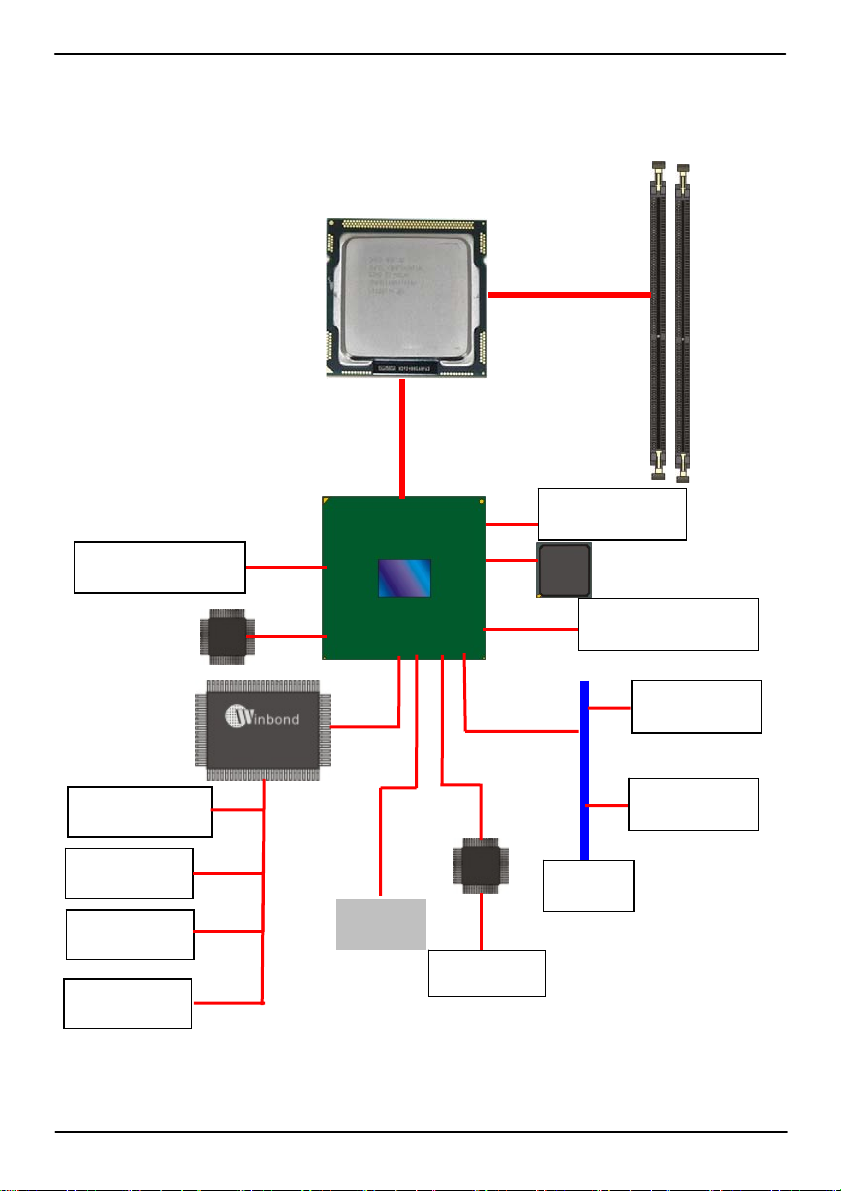
1.3 <Block Diagram>
4 x 240-pin DDR3
1066/1333MHz up
to 32GB
6 x Serial ATA
12 x USB2.0 ports
HD Audio
2 x Serial ports
IrDA
8-bit GPIO
Parallel port
Intel Q67
SPI
BIOS
Intel 82574L
2 x GLAN
Mini-PCIe card slot
PCI-E x16 & x4
Mini-PCI slot
5 x PCI slot
PCI bus
COM3/4/5/6
10
Page 11
AS-C74 User’s Manual
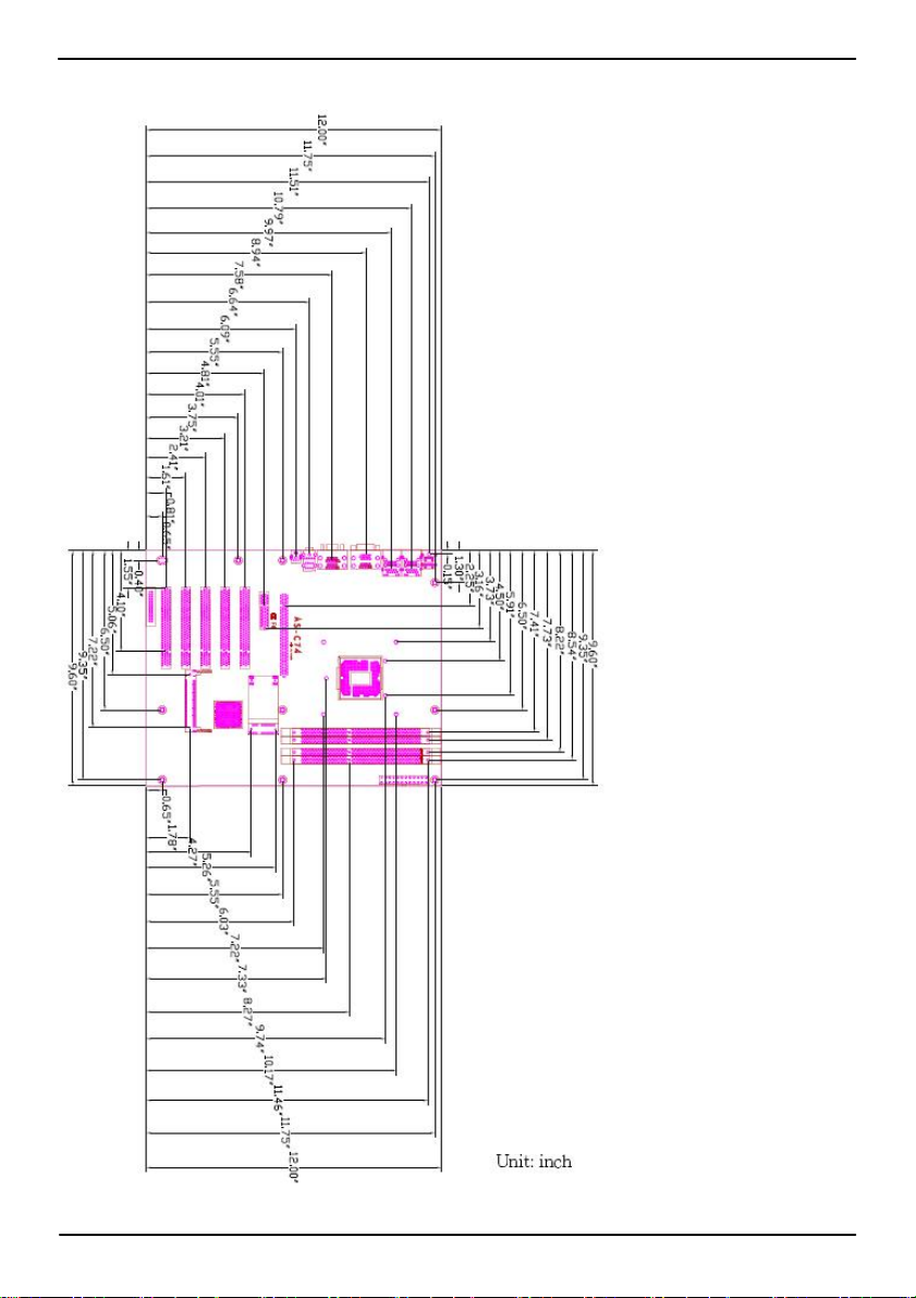
1.4 <Mechanical Drawing >
11
Page 12
AS-C74 User’s Manual
Chapter 2 <Hardware Setup>
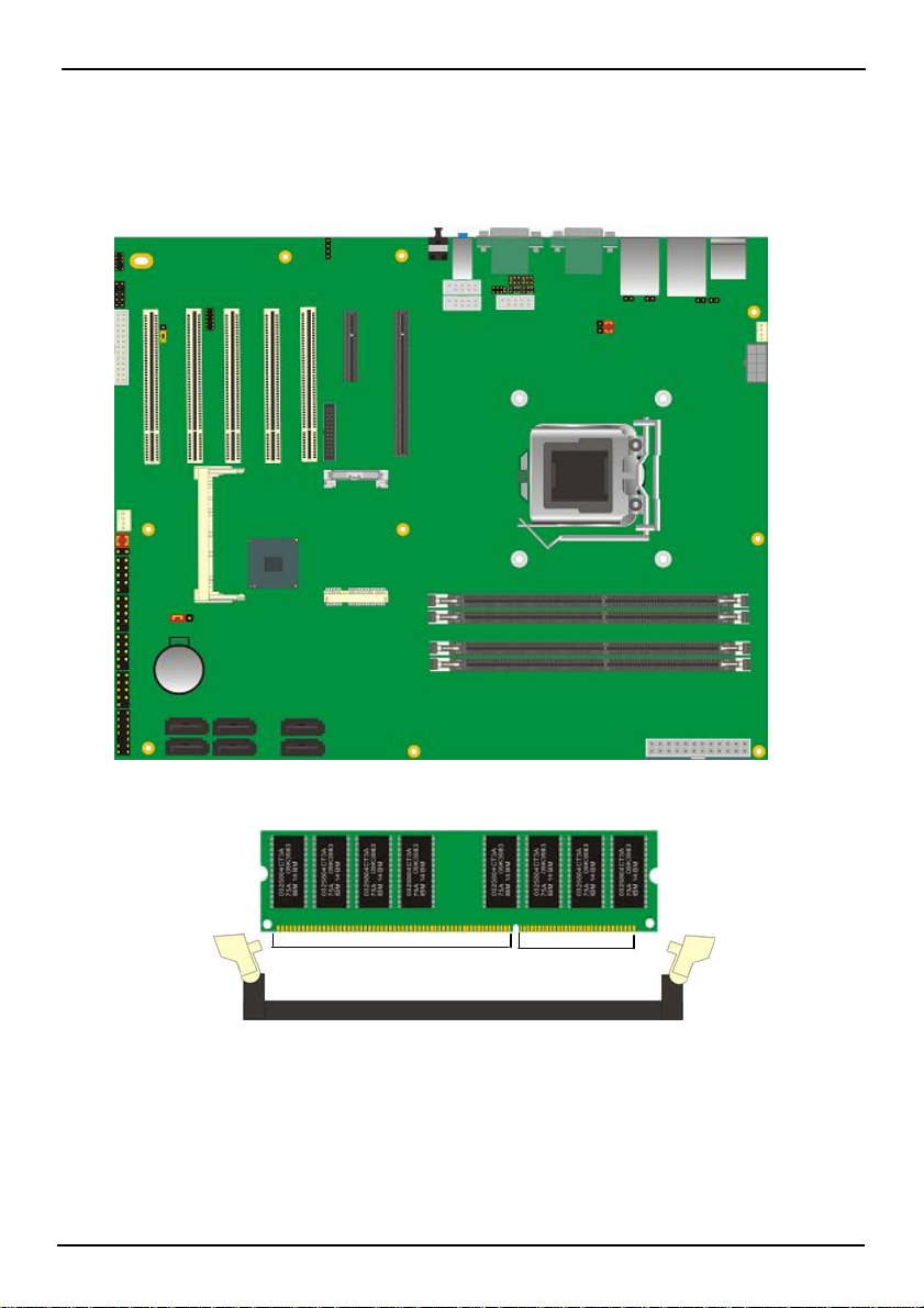
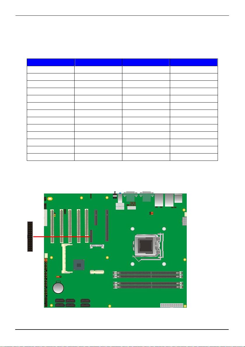
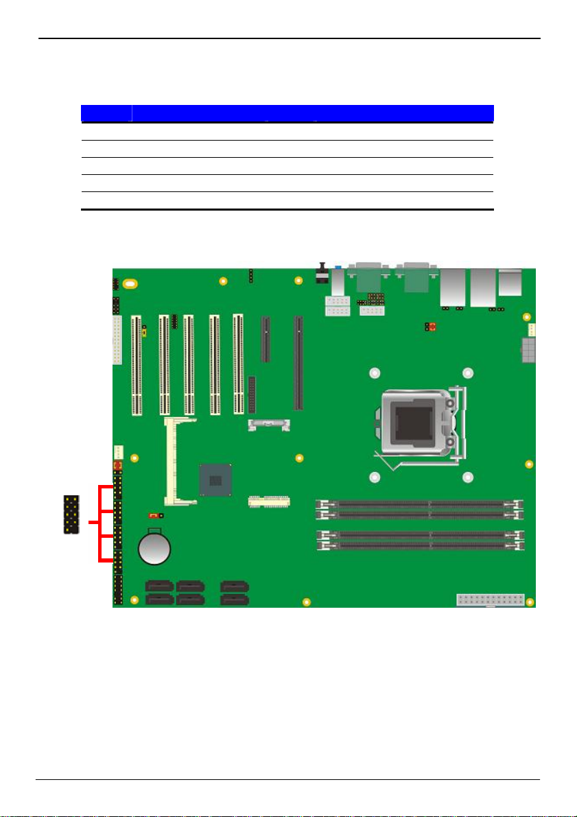
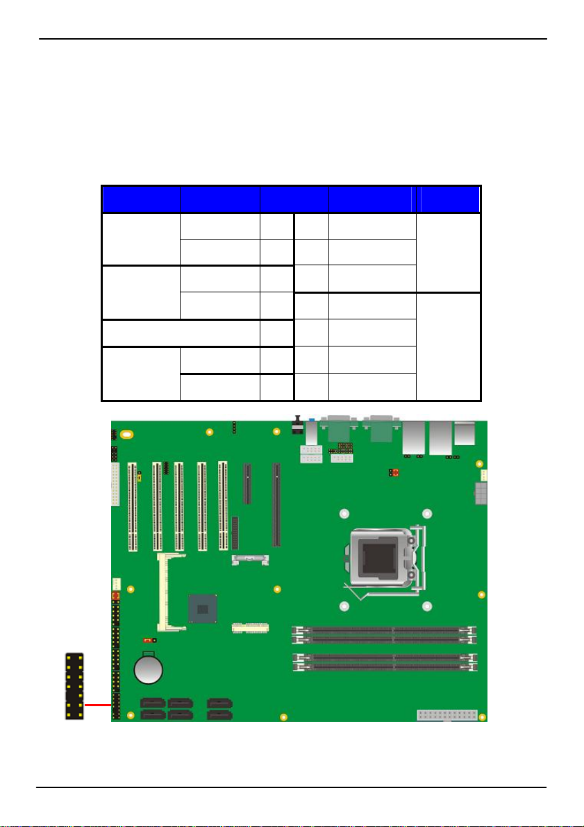
2.1 <Connector Location>
CN_AUDIO
LPT
CN_DVI
SYSFAN
CN_USB1/2
JFRNT
CN_DIO
S_ATA1/2/3/4/5/6
CDIN
CPUFAN
CN_12V
ATX
DDRIIIA1/2/B1/2
RJ45_1/2
COM1 COM3
PS2
USB CRT COM2
SPDIF
Audio
12
Page 13
AS-C74 User’s Manual
2.2 <Jumper Reference>
Jumper Function
JRTC CMOS Operating/Clear Setting
JP1 COM1 signal mode switch (For Pin-1 & Pin-9)
JP2 COM2 signal mode switch (For Pin-1 & Pin-9)
JAT Power mode select
JCSEL1
JCSEL2
JVUSB1/2
JAT
JVUSB1
1 2
5 6
Jumper: JAT
Type: Onboard 3-pin jumper
JAT Mode
1-2 AT Power mode
2-3 ATX Power mode
Default setting
Jumper: JVUSB1/2
Type: Onboard 6-pin jumper
JVUSB Mode
1-3 & 2-4 5V
3-5 & 4-6 5V_SB
Default: 1-3 & 2-4
CN_COM2 RS-232 RS422 RS485 Setting
CN_IR IrDA Setting
USB Voltage Setting
JAT
1
3
1 2
5 6
JVUSB2
5 1
6 2
Connector Reference 13
Page 14
AS-C74 User’s Manual
2.3 <Connector Reference>
2.3.1 <Internal Connectors>
Connector Function Remark
CPU LGA1155 CPU socket
DDRIIIA1/2&B1/2 240 –pin DDR3 SDRAM DIMM socket
S_ATA1/2/3/4/5/6 7-pin Serial ATA II connector
ATX 24-pin power supply connector
CN_12V 8-pin +12V additional power supply connector
CN_AUDIO 5 x 2-pin audio connector
CDIN 4-pin CD-ROM audio input connector
CN_DIO 6 x 2-pin digital I/O connector
CN_USB1/2/3/4 10-pin USB connector
CPUFAN 4-pin CPU cooler fan connector
SYSFAN 3-pin system cooler fan connector
CN_IR 5-pin IrDA connector
CN_SMBUS 5-pin SMBUS connector
JFRNT 14-pin front panel switch/indicator connector
PCIE_16X PCI Express 16x slot
PCIE_4X PCI Express 4x slot
Mini-PCI 1 x Mini-PCI socket
PCI 5 x PCI slots
CN_DVI 26 Pin connector
CN_COM4/5/6 5 x 2-pin com connector
MINI_CARD 1 x 52-pin PCI Express mini card
LPT 26-pin LPT port connector
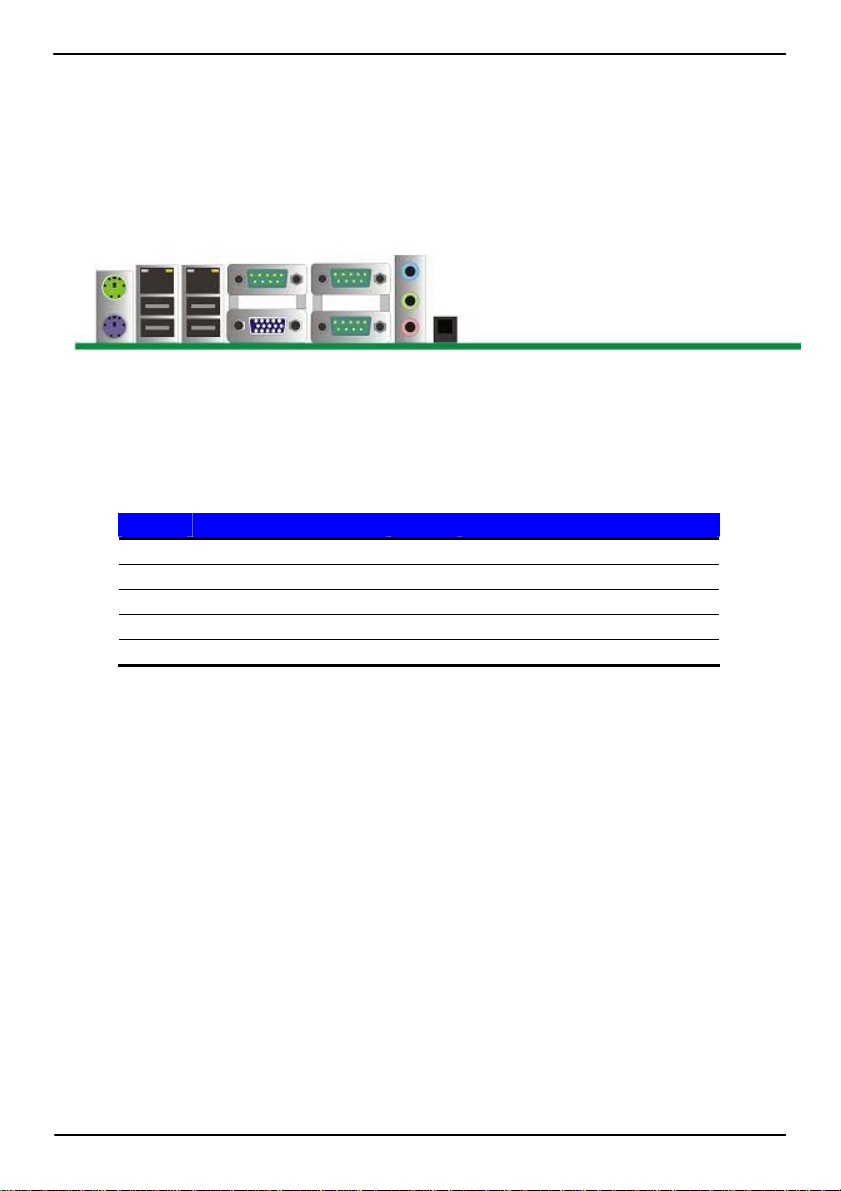
2.3.2 <External Connectors>
Connector Function Remark
PS2 PS/2 Keyboard /Mouse connector
CRT+COM1 DB15 VGA + Serial port connector
USB_RJ45_1/2 Dual USB and one RJ45 LAN Port
COM 2/3 Serial port connector
AUDIO Audio connectors
SPDIF SPDIF digital audio output connector
14
Page 15
AS-C74 User’s Manual
p
2.4 <CPU and Memory Setup>
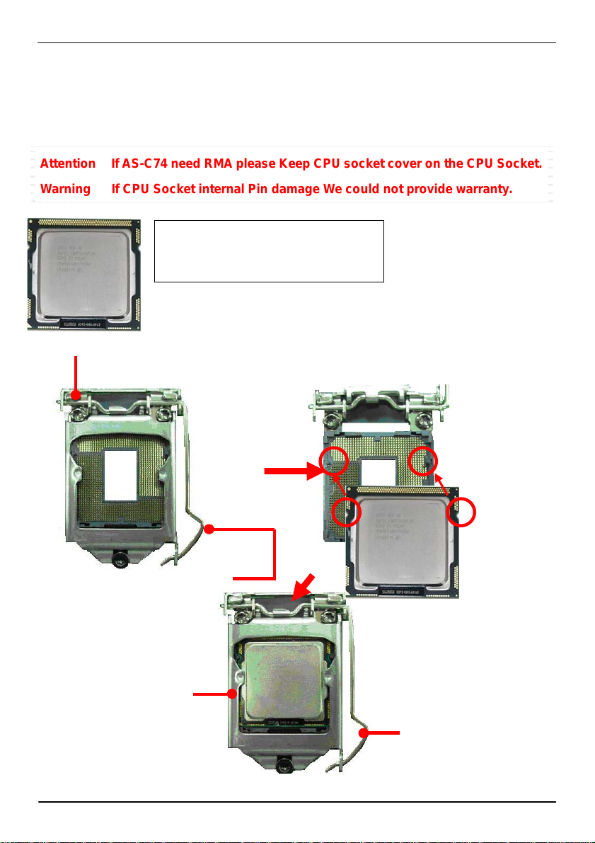
2.4.1 <CPU installation>
AS-C74 has a LGA1155 CPU socket onboard; please check following steps to install the
processor properly.
Attention If AS-C74 need RMA please Keep CPU socket cover on the CPU Socket.
Warning If CPU Socket internal Pin damage We could not provide warranty.
Intel® I 3/I5/I7/Pentium® processor
Package type: 1155 pin FCLGA
FSB:1066/1333MHz
1. Lift this bar
4. Lock this bar
2. Uncover this plate
Checked point
3. Place the CPU on the top of
ins
the
3. Cover this plate
Notice: Please place the CPU on the pins tenderlyto avoid bending the pins
15
Page 16
AS-C74 User’s Manual
2.4.2 <Memory installation>
AS-C74 has four 240-pin DDR3 DIMM support up to 32GB of memory capacity. The
memory frequency supports 1066/1333 MHz. Only Non-ECC memory is supported.
DDR3 A1/2
DDR3 B1/2
144-pin
Please check the pin number to match the socket side well
before installing memory module.
96-pin
16
Page 17

AS-C74 User’s Manual
2.5 <CMOS Setup>
The board’s data of CMOS can be setting in BIOS. If the board refuses to boot due to
inappropriate CMOS settings, here is how to proceed to clear (reset) the CMOS to its
default values.
Jumper: JRTC
Type: Onboard 3-pin jumper
JRTC Mode
1-2 Clear CMOS
2-3 Normal Operation
Default setting
3 1
JRTC
17
Page 18

AS-C74 User’s Manual
2.6 <Serial ATA installation>
AS-C74 has Four Serial ATA II & Two Serial ATA III interfaces with RAID function, the
transfer rate of the Serial ATA II can be up to 300MB/s & Serial ATA III can be up to 600MB/s.
Please go to http://www.serialata.org/
for more about Serial ATA technology information.
Based on Intel® PCH, it supports Intel® Matrix Storage Technology with combination of
RAID 0,1,5 and 10. The main features of RAID on Intel® Q67 PCH are listed below:
1. Supports for up to RAID volumes on a single, two-hard drive RAID array.
2. Supports for two, two-hard drive RAID arrays on any of six Serial ATA ports.
3. Supports for Serial ATA ATAPI devices.
4. Supports for RAID spares and automatic rebuild.
5. Supports on RAID arrays, including NCQ and native hot plug.
For more information please visit Intel’s official website.
For more about the system setup for Serial ATA, please check the chapter of SATA
configuration.
SATA1/3/5
SATA2/4/6
SATAII SATAIII
18
Page 19
AS-C74 User’s Manual
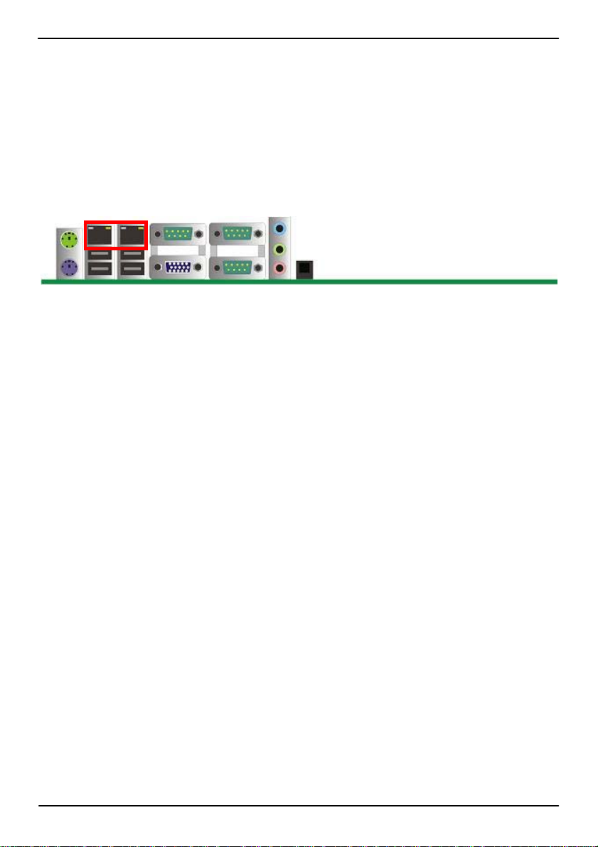
2.7 <LAN installation>
The board integrates with two Intel 82574L Gigabit Ethernet controllers, as the PCI Express
bus. The Intel 82574L supports triple speed of 10/100/1000Base-T, with IEEE802.3
compliance and Wake-On-LAN supported.
LAN2 LAN1
LAN Installation 19
Page 20
AS-C74 User’s Manual
2.8 <Onboard Display Interface>
Based on Intel Q67 chipset with built-in graphics, the board provides one DB15 Connect or
on real external I/O port and the board also provides 26-pin DVI interface
Notice: When you install any PCI Graphic card, the onboard graphics would be disabled
automatically.
2.8.1 <Analog Display>
Please connect your CRT or LCD monitor with DB15 male connector to the onboard DB15
female connector on rear I/O port.
CRT
20
Page 21
AS-C74 User’s Manual
2.8.2 <DVI Display >
The board also comes with a DVI interface with Chrontel for digital video interface.
Connector: CN_DVI
Connector type: 26-pin header connector (pitch = 2.00mm)
Pin Number Assignment Pin Number Assignment
1 TX1+ 2 TX13 Ground 4 Ground
5 TXC+ 6 TXC7 Ground 8 PVDD
9 N/C 10 N/C
11 TX2+ 12 TX213 Ground 14 Ground
15 TX0+ 16 TX017 N/C 18 HPDET
19 DDCDATA 20 DDCCLK
21 GND 22 N/C
23 N/C 24 N/C
25 N/C 26 N/C
CN_DVI
25 26
1 2
21
Page 22

AS-C74 User’s Manual
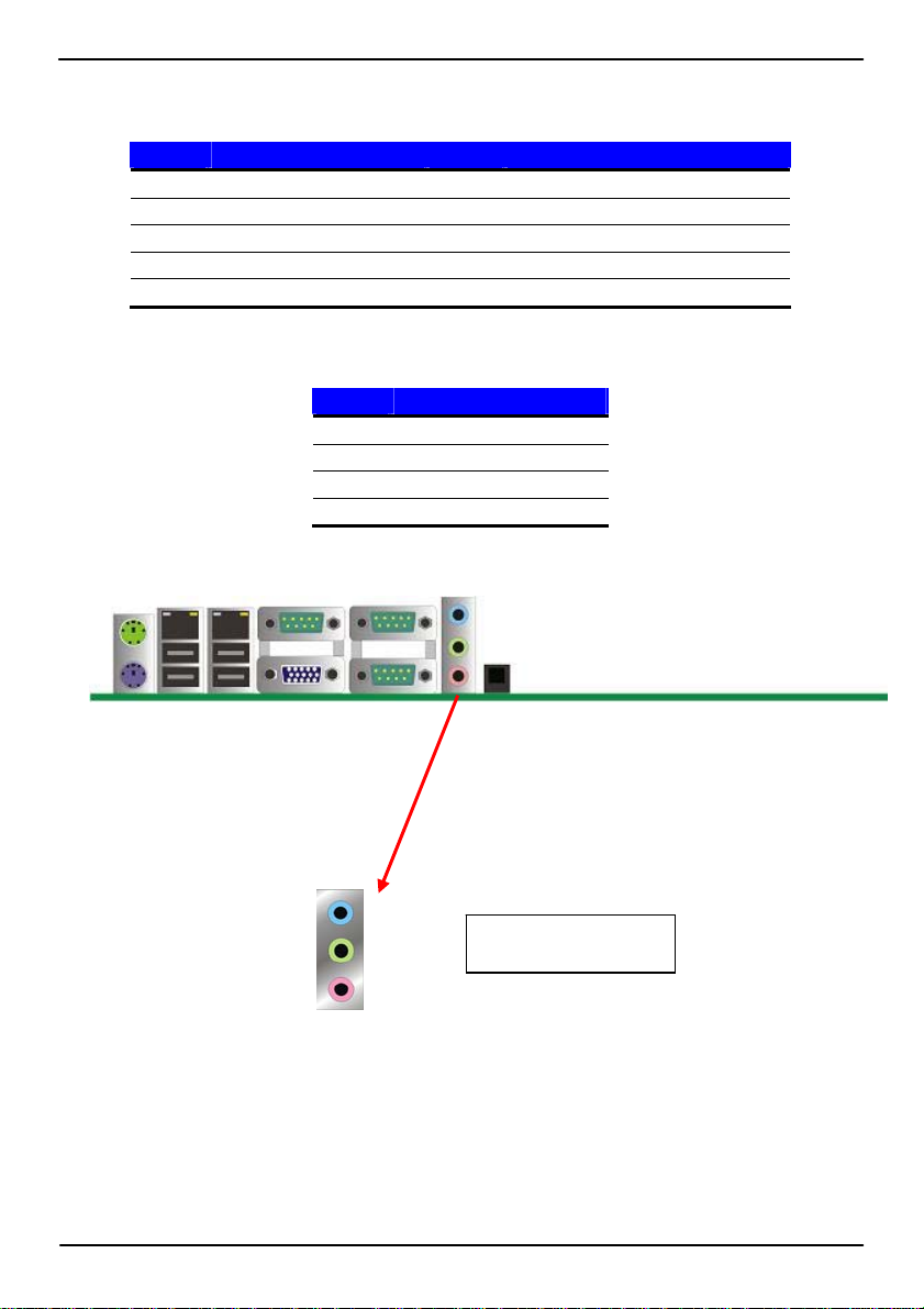
2.9 <Audio Installation>
The board integrates onboard audio interface with REALTEK ALC888 codec, with Intel next
generation of audio standard as High Definition Audio, it offers more vivid sound and oth er
advantages than former HD audio compliance.
The main specifications of ALC888 are:
z High-performance DACs with 100dB S/N ratio
z 2 DAC channels support 16/20/24-bit PCM format for 2 audio solution
z 16/20/24-bit S/PDIF-OUT supports 44.1K/48K/96kHz sample rate
z Compatible with HD
z Meets Microsoft WHQL/WLP 2.0 audio requirements
The board provides 2 channels audio phone jacks on rear I/O port, Line-in/MIC-in ports for
front I/O panel through optional cable.
CDIN
CN_AUDIO
1
2
10
9
1
4
22
Page 23
AS-C74 User’s Manual
Connector: CN_AUDIO
Type: 10-pin (2 x 5) header (pitch = 2.54mm)
Pin Description Pin Description
1 MIC_L 2 Ground
3 MIC_R 4 ACZ_DET
5 Speaker_R 6 MIC Detect
7 SENSE 8 N/C
9 Speaker_L 10 Speaker Detect
Connector: CDIN
Type: 4-pin header (pitch = 2.54mm)
Pin Description
1 CD – Left
2 Ground
3 Ground
4 CD – Right
LINE-IN
LINE-OUT
MIC-IN
23
Rear I/O phone jacks
Page 24
AS-C74 User’s Manual
2.10 <GPIO and SMBUS interface>
The board provides a programmable 8-bit digital I/O interface, and a SMBUS (System
management bus) interface for control panel application.
Connector: CN_DIO
Type: onboard 2 x 6-pin header, pitch=2.0mm
Pin Description Pin Description
1 Ground 2 Ground
3 GP10 4 GP14
5 GP11 6 GP15
7 GP12 8 GP16
9 GP13 10 GP17
11 VCC 12 +12V
CN_SMBUS
5
1
1 2
11 12
Connector: CN_SMBUS
Type: 5-pin header for SMBUS Ports
24
Pin Description
1 VCC
2 N/C
3 SMBDATA
4 SMBCLK
5 Ground
Page 25
AS-C74 User’s Manual
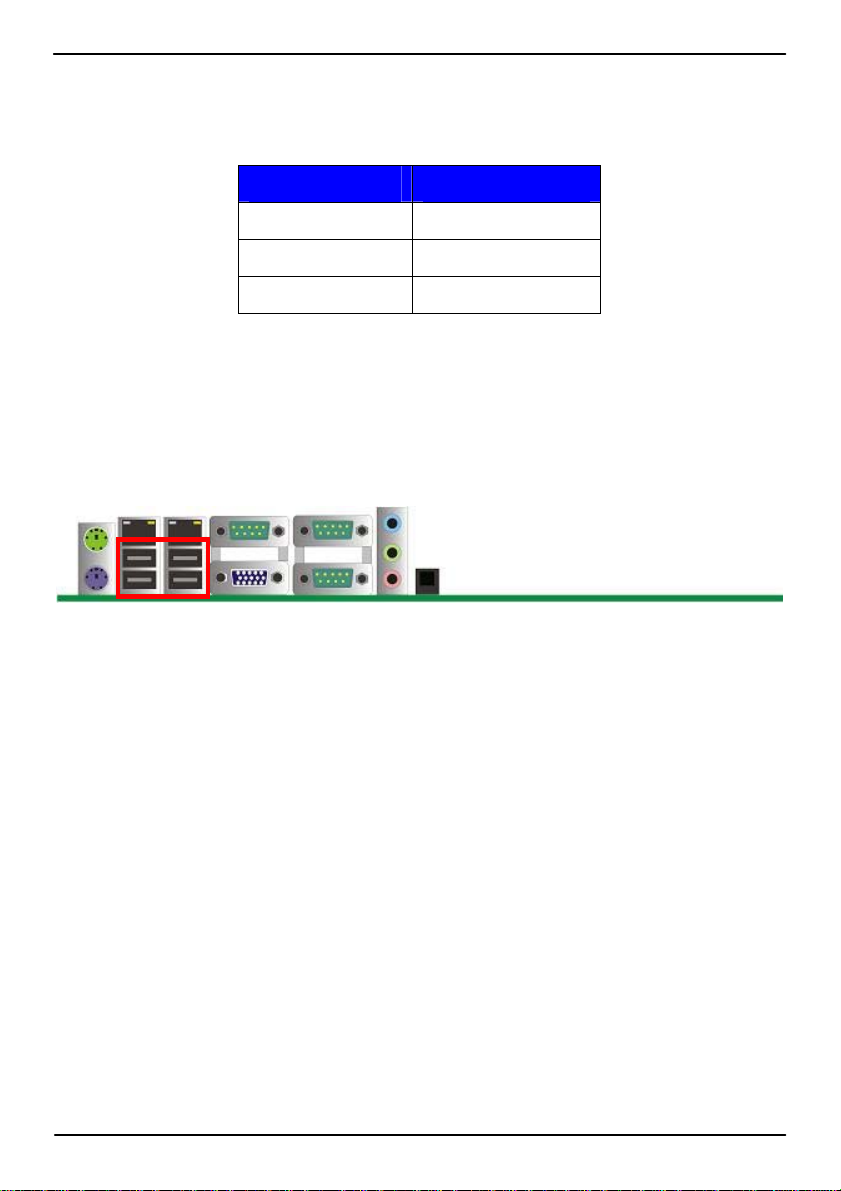
2.11 <USB Installation>
AS-C74 integrates eight USB2.0 ports. The specifications of USB2.0 are listed below:
Interface USB2.0
Controller Intel Q67 PCH
Transfer Rate Up to 480Mb/s
Voltage 5V
The Intel® Q67 contains two Enhanced Host Controller Interface (EHCI) and five Universal
Host Controller Interfaces (UHCI), it can determine whether your connected device is for
USB1.1 or USB2.0, and change the transfer rate automatically.
USB3/4/5/6
25
Page 26
AS-C74 User’s Manual
Connector: CN_USB1/2
Type: 10-pin (5 x 2) header for USB5/6 Ports
Pin Description Pin Description
1 VCC 2 VCC
3 Data0- 4 Data15 Data0+ 6 Data1+
7 Ground 8 Ground
9 Ground 10 N/C
CN_USB1/2/3/4
1 2
9 10
26
Page 27
AS-C74 User’s Manual
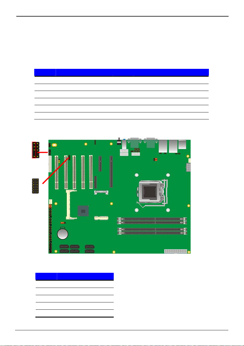
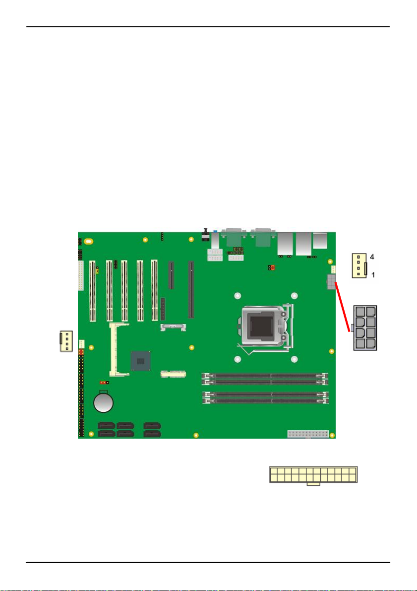
2.12 <Power and Fan Installation>
The AS-C74 provides a standard ATX power supply with 24-pin ATX connector and
additional 12V connector, and the board provides one 4-pin fan connectors supporting
smart fan for CPU cooler and one 3-pin cooler fan connectors for system and Northbridge
chip. The 8-pin CN_12V additional power connector is necessary for CPU powering; please
connect this well before you finishing the system setup.
CPUFAN
CN_12V
5 1
1
4
8 4
1
13
12ATX
24
27
Page 28

AS-C74 User’s Manual
Connector: ATX
Type: 24-pin ATX power connector
PIN assignment
1 3.3V 13 3.3V
2 3.3V 14 -12V
3 GND 15 GND
4 5V 16 PS_ON
5 GND 17 GND
6 5V 18 GND
7 GND 19 GND
8 PW_OK 20 -5V
9 5V_SB 21 5V
10 12V 22 5V
11 12V 23 5V
12 3.3V 24 GND
Connector: CN_12V
Type: 8-pin standard Pentium 4 additional +12V power connector
Pin Description Pin Description
1 Ground 5 +12V
2 Ground 6 +12V
3 Ground 7 +12V
4 Ground 8 +12V
Connector: CPUFAN
Type: 4-pin fan wafer connector
Pin Description Pin Description
1 Ground 2 +12V
3 Fan Speed Detection 4 Fan Control
Connector: SYSFAN
Type: 4-pin fan wafer connector
Pin Description Pin Description
1 Ground 2 +12V
3 Fan Speed Detection 4 Fan Control
28
Page 29
AS-C74 User’s Manual
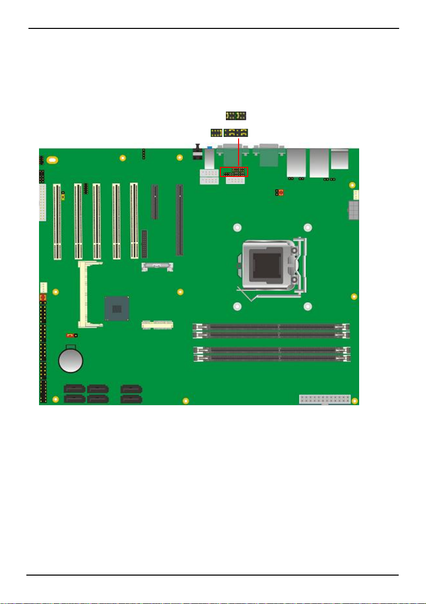
2.13 <Serial Port>
The board supports Three RS232 serial port and one jumper selectable RS232/422/485
serial ports. The jumper JCSEL1 & JCSEL2 can let you configure the communicating
modes for COM2.
Connector: COM2
Type: 9-pin header connector for COM2
Pin Description Pin Description
1 DCD/422TX-/485- 2 RXD/422TX+/485+
3 TXD/422RX+ 4 DTR/422RX5 GND 6 DSR
7 RTS 8 CTS
9 RI 10 N/C
COM1
COM3
COM2
29
Page 30
AS-C74 User’s Manual
Setting RS-232 & RS-422 & RS-485 for COM2
JP2 JP1
JCSEL2
JCSEL1
30
Page 31

AS-C74 User’s Manual
Function JCSEL2 JCSEL1
SIR
RS-422
RS-485
RS-232
Default setting:
JCSEL2: (1-2) JCSEL1: (1-3, 2-4, 7-9, 8-10)
Jumper: JP1 (COM 1)/ JP2(COM2)
Type: onboard 3 x 2-pin header
JP1/JP2 Mode
5-6 Standard COM Port
3-4 Pin9 with 12V signal
1-2 Pin9 with 5V signal
Default setting
7
1
8 2
7
1
8 2
1
7
8 2
1
7
8 2
2 6
1 5
1
2
1
2
1
2
1
2
11
12
11
12
11
12
11
12
31
Page 32
AS-C74 User’s Manual
2.14 <Switch and Indicator>
The JFRNT provides front control panel of the board, such as power button, reset and
beeper, etc. Please check well before you connecting the cables on the chassis.
Connector: JFRNT
Type: onboard 14-pin (2 x 7) 2.54-pitch header
Function Signal PIN Signal Function
IDE LED
Reset
Power
Button
HDLED+ 1 2 PWDLED+
Power
HDLED- 3 4 N/C
LED
Reset+ 5 6 PWDLED-
Reset- 7 8 SPKIN+
N/C 9 10 N/C
Speaker
PWRBT+ 11 12 N/C
PWRBT- 13 14 SPKIN-
JFRNT
1 2
13 14
32
Page 33

AS-C74 User’s Manual
(This Page is Left for Blank)
33
Page 34
AS-C74 User’s Manual
Chapter 3 <System Configuration>
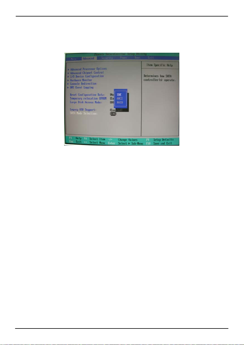
3.1 <SATA configuration>
SA TA Mode:
This option can let you select whether the Serial ATA hard drives would work under normal
IDE mode or RAID mode. The RAID mode need more than one HDD is applied.
34
Page 35

AS-C74 User’s Manual
3.2 <SATA RAID Configuration>
The board integrates Intel® Q67 PCH with RAID function for Serial ATA II drives, and
supports the configurations below:
RAID 0 (Stripping): Two hard drives operating as one drive for optimized data R/W
performance. It needs two unused drives to build this operation.
RAID 1 (Mirroring): Copies the data from first drive to second drive for data security, and if
one drive fails, the system would access the applications to the workable drive. It needs two
unused drives or one used and one unused driv e to build this operation. The second drive
must be the same or lager size than first one.
RAID 5 (striping with parity)
A RAID 5 array contains three or more hard drives where the data is divided into
manageable blocks called strips. Parity is a mathematical method for recreating data that
was lost from a single drive, which increases fault-tolerance. The data and parity are striped
across all the hard drives in the array. The parity is striped in a rotating sequence to reduce
bottlenecks associated with the parity calculations.
RAID 10 (RAID 0+1)
A RAID 10 array uses four hard drives to create a combination of RAID levels 0 and 1. The
data is striped across a two-drive array forming the RAID 0 component. Each of the drives
in the RAID 0 array is then mirrored by a RAID 1 component.
Intel Matrix Storage Technology: This technology would allow you to use RAID 0+1 mode
on only two drives (4 drives needed on traditional RAID 0+1). It will create two partitions on
each hard drive to simulate RAID 0 and RAID 1. It also can let you modify the partition size
without re-formatted.
For more information of Intel Matrix Storage Technology, please visit Intel’s website.
If you need to install an operation system on the RAID set, please use the driver disk
attached in the package when it informs you to obtain the RAID drivers.
35
Page 36
AS-C74 User’s Manual
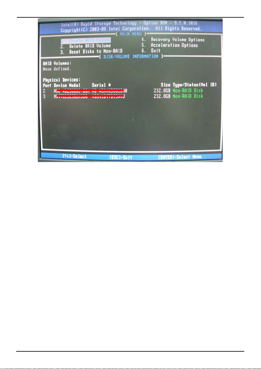
Please press <CTRL+I> to enter the RAID configuration menu.
You can setup the RAID under operation system for Microsoft® Windows XP SP1, please
install the Intel® Application Accelerator Ver.4.5 later to support RAID configuration with
Intel® Matrix Storage Technology.
36
Page 37
AS-C74 User’s Manual
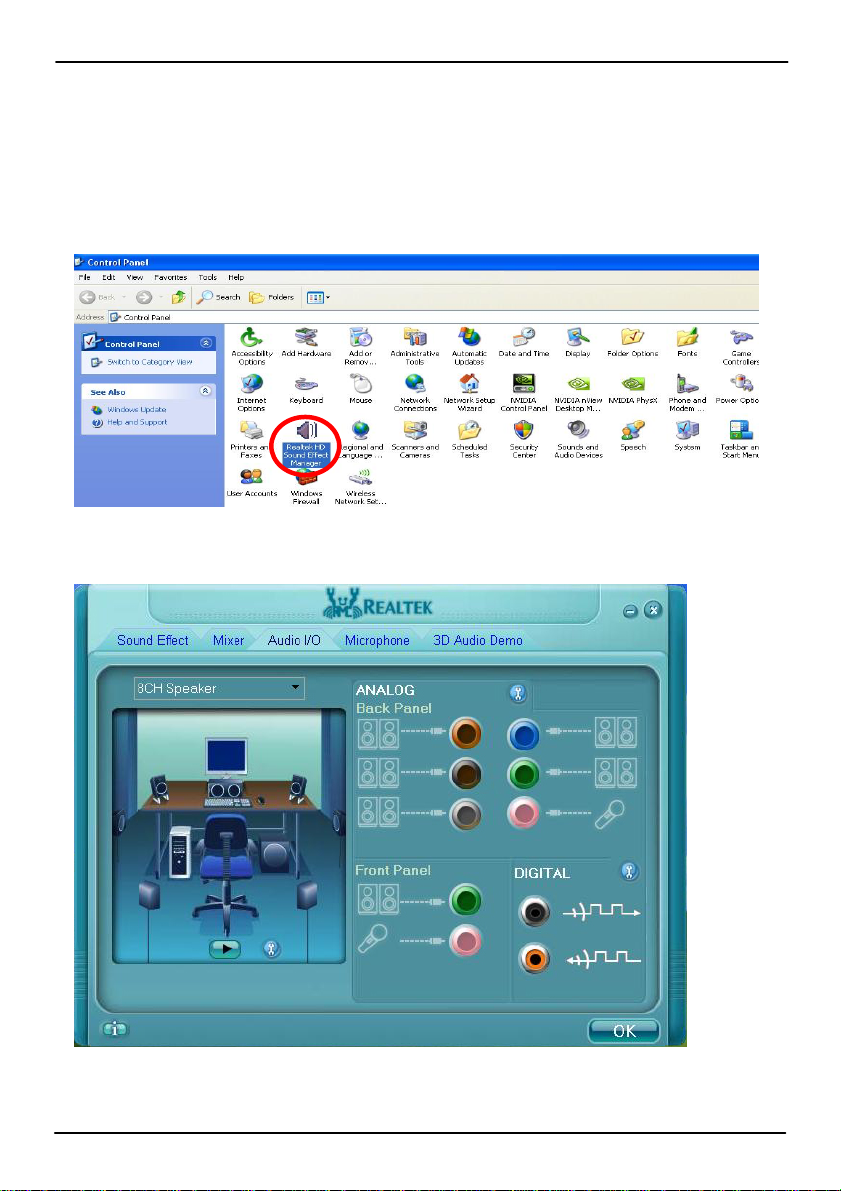
3.3 <Audio Configuration>
The board integrates Intel® Q67 PCH with REALTEK® ALC888 codec. It can support
2-channel sound under system configuration. Please follow the steps below to setup your
sound system.
1. Install REALTEK HD Audio driver.
2. Lunch the control panel and Sound Effect Manager.
3. Select Speaker Configuration
4. Select the sound mode to meet your speaker system.
37
Page 38
AS-C74 User’s Manual
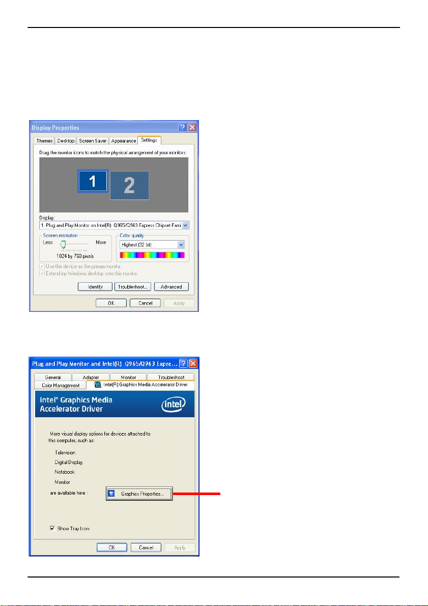
3.4 <Display Properties Setting>
Based on Intel Q67 with HD Graphic, the board supports two DACs for display device as
different resolution and color bit.
Please install the Intel Graphic Driver before you starting setup display devices.
1. Click right button on the desktop to lunch display properties
2. Click Advanced button for more specificity setup.
Click Graphics Properties... for
advanced setup
38
Page 39
AS-C74 User’s Manual
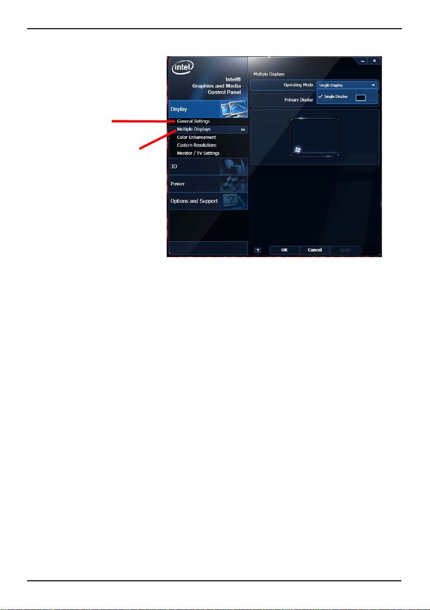
4. This setup options can let you define each device settings.
Click Monitor to setup the CRT
monitor for Colors, Resolution
and Refresh Rate
Click Intel® Dual Display
Clone to setup the dual
display mode as same screen
39
Page 40

AS-C74 User’s Manual
Chapter 4 <BIOS Setup>
The motherboard uses the Phoenix BIOS for the system configuration. The Phoenix
BIOS in the single board computer is a customized version of the industrial standard
BIOS for IBM PC AT-compatible computers. It supports Intel x86 and compatible CPU
architecture based processors and computers. The BIOS provides critical low-level
support for the system central processing, memory and I/O sub-systems.
The BIOS setup program of the single board computer let the customers modify the
basic configuration setting. The settings are stored in a dedicated battery-backed
memory, NVRAM, retains the information when the power is turned off. If the battery
runs out of the power, then the settings of BIOS will come back to the default setting.
The BIOS section of the manual is subject to change without notice and is provided here
for reference purpose only. The settings and configurations of the BIOS are current at
the time of print, and therefore they may not be exactly the same as that displayed on
your screen.
To activate CMOS Setup program, press <DEL> key i mmediately after you turn on
the system. The following message “Press DEL to enter SETUP” should appear in the
lower left hand corner of your screen. When you enter the CMOS Setup Utility, the Main
Menu will be displayed as Figure 4-1. You can use arrow keys to select your function,
press <Enter> key to accept the selection and enter the sub-menu.
Figure 4-1 CMOS Setup Utility Main Screen
40
Page 41

AS-C74 User’s Manual
(This Page is Left for Blank)
41
Page 42
AS-C74 User’s Manual
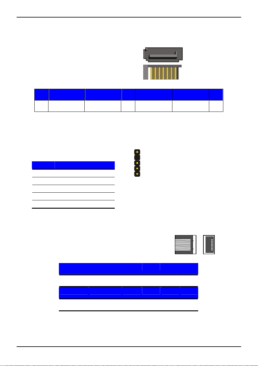
Appendix A <I/O Port Pin Assignment>
A.1 <Serial ATA Port>
Connector: S_ATA1/2/3/4/5/6
Type: 7-pin wafer connector
1 2 3 4 5 6 7
GND RSATA_TXP1 RSATA_TXN1 GND RSATA_RXN1 RSATA_RXP1 GND
17
A.2 <IrDA Port>
Connector: CN_IR
Type: 5-pin header for SIR Ports
Pin Description
1 VCC
2 N/C
3 IRRX
4 Ground
5 IRTX
1
5
A.3 <LAN Port>
Connector: RJ451/2
Type: RJ45 connector with LED on bracket
Pin 1 2 3 4 5
Description TRD0+ TRD0- TRD1+ TRD2+ TRD2-
Pin 6 7 8 9 10
Description TRD1- TRD3+ TRD3- NC NC
42
Page 43
AS-C74 User’s Manual
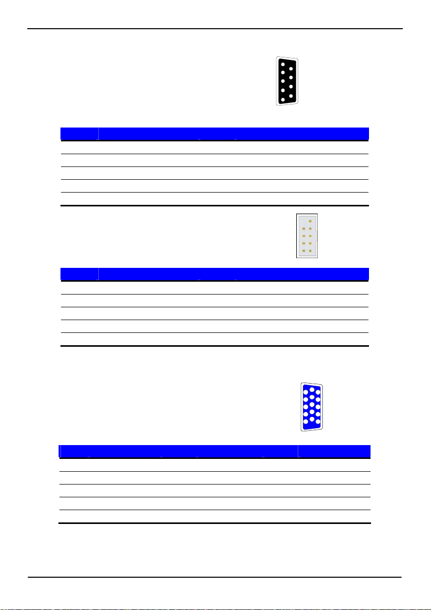
A.4 <Serial Port>
Connector: COM1/2/3
Type: 9-pin D-sub male connector on bracket
Pin Description Pin Description
1 DCD 6 DSR
2 SIN 7 RTS
3 SO 8 CTS
4 DTR 9 RI
5 Ground
Connector: CN_COM4/5/6
Type: 9-pin D-sub male connector on bracket
Pin Description Pin Description
1 DCD 6 DSR
2 SIN 7 RTS
3 SO 8 CTS
4 DTR 9 RI
5 Ground
1
2
3
4
5
10
2
6
7
8
9
9
1
A.5 <VGA Port>
Connector: CRT
Type: 15-pin D-sub female connector on bracket
Pin Description Pin Description Pin Description
1 RED 6 Ground 11 N/C
2 GREEN 7 Ground 12 DDC_DA
3 BLUE 8 Ground 13 HSYNC
4 N/C 9 +5V 14 VSYNC
5 Ground 10 Ground 15 DDC_CLK
6
1
2
3
4
5
10
11
12
13
14
15
43
Page 44

AS-C74 User’s Manual
A.6<Parallel Port>
Connector: LPT (PRINTER)
14
Type: 26-pin (2 x 13) 2.54-pitch box header
1
Pin Description Pin Description
1 STROBE- 14 AUTO FEED-
2 D0 15 ERROR3 D1 16 INITIALIZE4 D2 17 SELECT INPUT5 D3 18 Ground
6 D4 19 Ground
7 D5 20 Ground
8 D6 21 Ground
9 D7 22 Ground
10 ACKNOWLEDGE- 23 Ground
11 BUSY 24 Ground
12 PAPER EMPTY 25 Ground
13 SELECT+ 26 N/C
26
13
44
Page 45

AS-C74 User’s Manual
Appedix B <System Resources>
B.1 <I/O Port Address Map>
45
Page 46
AS-C74 User’s Manual
46
Page 47

AS-C74 User’s Manual
B.2 <Memory Address Map>
47
Page 48
AS-C74 User’s Manual
B.3 <System IRQ Resources>
48
Page 49

AS-C74 User’s Manual
Appendix C <Programming GPIO’s>
The GPIO’can be programmed with the MSDOS debug program using simple
IN/OUT commands.The following lines show an example how to do this.
GPIO0…..GPIO7 bit0……bit7
-o 2E 87 ;enter configuration
-o 2E 87
-o 2E 07
-o 2F 09 ;enale GPIO function
-o 2E 30
-o 2F 02 ;enable GPIO configuration
-o 2E F0
-o 2F xx ;set GPIO as input/output; set ‘1’ for input,’0’for output
-o 2E F1
-o 2F xx ;if set GPIO’s as output,in this register its value can be set
Optional :
-o 2E F2
-o 2F xx ; Data inversion register ; ‘1’ inverts the current valus of the bits ,’0’
leaves them as they are
-o 2E 30
-o 2F 01 ; active GPIO’s
For further information ,please refer to Winbond W83627DHG-P datasheet.
49
Page 50

AS-C74 User’s Manual
Appendix D <Watch Dog timer Setting >
The watchdog timer makes the system auto-reset while it stops to work for a period. The
integrated watchdog timer can be setup as system reset mode by program.
Timeout Value Range
- 1 to 255
- Second or Minute
Program Sample
Watchdog timer setup as system reset with 5 second of timeout
2E, 87
2E, 87
2E, 07
2F, 08 Logical Device 8
2E, 30 Activate
2F, 01
2E, F5 Set as Second*
2F, 00
2E, F6 Set as 5
2F, 05
* Minute: bit 3 = 0; Second: bit 3 = 1
You can select Timer setting in the BIOS, after setting the time options, the system will
reset according to the period of your selection.
50
Page 51
AS-C74 User’s Manual
Contact Information
Any advice or comment about our products and service, or anything
we can help you please don’t hesitate to contact with us. We will do
our best to support you for your products, projects and business.
Taiwan Commate Computer Inc.
19F . , No.94, Sec. 1, Xintai 5th Rd., Xizhi Dist., New Taipei City
Address
TEL +886-2-26963909
FAX +886-2-26963911
22102, Taiwan
Website
E-Mail
Facebook
Twitter https://twitter.com/Taiwan_Commate
TUhttp://www.commell.com.twUT
TUinfo@commell.com.twUT (General Information)
TUtech@commell.com.twUT (Technical Support)
https://www.facebook.com/pages/Taiwan-Commate-Computer-Inc/547993955271899
Commell is a brand name of Taiwan commate computer Inc.
Contact Information
51
 Loading...